Force Computers GmbH All Rights Reserved This document shall not be duplicated, nor its contents used for any purpose, unless written permission has been granted. Copyright by Force Computers PENT/CPCI-731 Reference Guide P/N 211604 Edition 1.2 May 2000
Transcript
Force Computers GmbHAll Rights Reserved
This document shall not be duplicated, nor its contents usedfor any purpose, unless written permission has been granted.
Copyright by Force Computers
PENT/CPCI-731Reference Guide
P/N 211604 Edition 1.2May 2000
World Wide Web: www.forcecomputers.com 24-hour access to on-line manuals, driver updates, and application notes is provided via SMART, our SolutionsPLUS customer support program
that provides current technical and services information.
Headquarters
The Americas Europe Asia
Force Computers Inc.5799 Fontanoso WaySan Jose, CA 95138-1015U.S.A.
The information in this document has been carefully checked and is believed to be entirely reliable. Force Computers makes no warranty of any kind with regard to the material in this document, and assumes no responsibility for any errors which may appear in this document. Force Computers reserves the right to make changes without notice to this, or any of its products, to improve reliability, performance, or design.
Force Computers assumes no responsibility for the use of any circuitry other than circuitry which is part of a product of Force Computers GmbH. Force Computers does not convey to the purchaser of the product described herein any license under the patent rights of Force Computers GmbH nor the rights of others. All product names mentioned herein are the trademarks or registered trademarks of their respective companies.
Copyright 2000 by Force Computers. All rights reserved. This document shall not be reproduced, transmitted, or stored in a retrieval system, nor its contents used for any purpose, without the prior written consent of Force Computers GmbH.
This section does not provide information on the product, but on standardfeatures of the manual itself:
• Its structure
• Special layout conventions
• Related documents
Audience of the Manual
This Reference Guide is intended for hard- and software developers stalling and integrating the PENT/CPCI-731 into their systems.
Overview of the Manual
This Reference Guide provides a comprehensive hardware and softwguide to your board.
Note: Please take a moment to examine the “Table of Contents” tosee how this documentation is structured. This will be of value to youwhen looking for information in the future.
It includes:
• Brief overview of the PENT/CPCI-731: see section 2 “Introductioon page 5.
• Installation instructions for powering up the board: see sectio“Installation” on page 9. It includes the default configuratio(switches and the like), initialization, connector pinouts, and BIOS details.
• Block diagram relating the most important components and a destion of the PENT/CPCI-731 specific registers: section 4 “Hardwaon page 33.
PENT/CPCI-731 Page ix
Using This Manual
2116
04 1
– 2
May
200
0
ical,
66
)”
al
Data Sheets It is assumed that the PENT/CPCI-731 is integrated into systems at theoperating system level. Therefore, no data sheets are provided in this Ref-erence Guide. Nevertheless, all data sheets of the most important boardcomponents are listed below. They can be found on the respective com-pany’s webpage.
• Synchronous DRAM - Hitachi/Micron/Mitsubishi 8Mx8(M5M4V64S30A) (www.halsp.hitachi.com)
Page x PENT/CPCI-731
Using This Manual
d
e
o
nde
ahee
Table a History of Manual Publication
Edition Date Description
1.0 December 1999 First Print
1.1 January 2000 Corrected Forced Air Flow intable 4 “Environmental Require-ments of the PENT/CPCI-731” onpage 9; corrected table 19 “NMI ControlRegister” on page 51;editorial changes
1.2 May 2000 Corrected IRQ settings in table 29“Hot Swap ENUM Register” onpage 67; changed SW2-3 to ON in table 6“PENT/CPCI-731 Switch Settings”on page 14; editorial changes
Table b Fonts, Notations and Conventions
Notation Description
All numbers are decimal numbers except when usewith the following notations:
0000.000016 Typical notation for hexadecimal numbers (digits ar0 through F), e.g. used for addresses and offsets.Note the dot marking the 4th (to its right) and 5th (tits left) digit.
00008 Same for octal numbers (digits are 0 through 7)
00002 Same for binary numbers (digits are 0 and 1)
Program Typical character format used for names, values, athe like. It is used to indicate when to type literally thsame word. Also used for on-screen output.
Variable Typical character format for words that represent part of a command, a programming statement, or tlike, and that will be replaced by an applicable valuwhen actually applied.
PENT/CPCI-731 Page xi
Using This Manual
2116
04 1
– 2
May
200
0
st –
Icons for Ease of Use: Safety Notes and Tips & Tricks
There are three levels of safety notes used in this manual which aredescribed below in brief by displaying a typical layout example.
Be sure to always read and follow the safety notes of a section firbefore acting as documented in the other parts of the section.
Danger Dangerous situation: injuries to people and severe damage to objectspossible.
Caution Possibly dangerous situation: no injuries to people but damage to ob-jects possible.
Note: No danger encountered. Pay attention to importantinformation marked using this layout.
Page xii PENT/CPCI-731
Safety Notes
1 Safety Notes
This section provides safety precautions to follow when installing, op-erating, and maintaining the PENT/CPCI-731. For your protection,follow all warnings and instructions found in the following text.
General This Reference Guide provides the necessary information to installand handle the PENT/CPCI-731. As the product is complex and itsusage manifold, we do not guarantee that the given information iscomplete. In case you need additional information, ask your ForceComputers representative.
The PENT/CPCI-731 has been designed to meet the standard indus-trial safety requirements. It must not be used except in its specificarea of office telecommunication industry and industrial control.
Only personnel trained by Force Computers or persons qualified inelectronics or electrical engineering are authorized to install, unin-stall or maintain the PENT/CPCI-731. The information given in thismanual is meant to complete the knowledge of a specialist and mustnot be taken as replacement for qualified personnel.
Make sure that contacts and cables of the board cannot be touchedwhile the board is operating.
Hot Swap The PENT/CPCI-731 provides hot-swap support, i.e. it may be in-stalled in or removed from a powered system supporting hot swap.Never install or uninstall the board in a system under hot-swap con-ditions unless the hot-swap or high-availability platform is used andthe system documentation explicitly includes appropriate guidelines.For detailed information on the hot-swap support and the relevantsafety notes, see “Hot Swap” on page 12. All of the following safetynotes refer to the installation and uninstallation of the board in anon-powered system.
Installation Electrostatic discharge and incorrect board installation and uninstal-lation can damage circuits or shorten their life. Therefore:
• Before installing or uninstalling the board, read section 3 “Instal-lation” on page 9.
• Before touching integrated circuits, ensure that you are workingin an ESD safe environment.
PENT/CPCI-731 Page 1
2116
04 1
– 2
May
200
0
Safety Notes
• Before installing or uninstalling the board in a CompactPCIrack:
– Check all installed boards for steps that have to be takenbefore turning off the power.
– Take those steps.
– Finally turn off the power.
• When plugging the board in or removing it, do not press on thefront panel but use the handles.
• Before installing or uninstalling an additional device or module,read the respective documentation.
• Ensure that the board is connected to the CompactPCI back-plane via all assembled connectors and that power is available onall power pins.
CompactPCI The PENT/CPCI-731 is a peripheral (or non host) board. Therefore:
• Plug the PENT/CPCI-731 only into a peripheral slot of a Com-pactPCI system.
• Never plug the PENT/CPCI-731 into another slot of a Compact-PCI system or into a system rack other than a CompactPCI sys-tem.
• Ensure that the board is connected to the CompactCI backplanevia all its connectors, and that power is available on all powerpins.
• When operating the board in areas of strong electro-magneticradiation, ensure that the board is:
– Bolted on the CompactPCI rack
– Shielded by enclosure
Hard Disk Limitation
If the PENT/CPCI-731/HD-AccKit is installed on thePENT/CPCI-731, the operating temperature and the shock and vi-bration values are limited by the hard disk environmental require-ments. For details, refer to the Installation Guide of the PENT/CPCI-731/HD-AccKit.
Power Consumption
The total maximal power consumption per PMC slot at +/–12 V, 5 V,and 3.3 V level must not exceed 7.5 W (total over all used voltages).
Page 2 PENT/CPCI-731
Safety Notes
r
r
a
o
Operation • While operating the board ensure that the environmental andpower requirements as given in table 4 “Environmental Require-ments of the PENT/CPCI-731” on page 9 and table 5 “Typical5 V and 3.3 V Power Requirements” on page 10 are met.
EMC • If boards are integrated into open systems, always cover emptyslots.
• The front panel of the PENT/CPCI-731 provides one cutout for aPMC module. If the board is shipped without the moduleinstalled, the front-panel cutout is covered by a blind panel toensure proper EMC shielding. To ensure proper EMC shielding,always operate the PENT/CPCI-731 with the blind panel or witha PMC module installed.
Expansion • Check the total power consumption of all components installed(see the technical specification of the respective components). Fothe total power consumption of the PENT/CPCI-731, see table 5“Typical 5 V and 3.3 V Power Requirements” on page 10.
• Ensure that any individual output current of any source stayswithin its acceptable limits (see the technical specification of therespective source).
• Only replace components or system parts with those recom-mended by Force Computers. In case you use components othethan those recommended by Force Computers, you are fullyresponsible for the impact on EMC/Safety and the eventuallychanged functionality of the product.
IOBP The IOBP-CPCI-731 is especially designed for the base board of thePENT/CPCI-731. Do not use any other I/O panels on thePENT/CPCI-731.
Environment Always dispose of used batteries and/or old boards according to yourcountry’s legislation.
Battery The board is designed to be maintenance-free. However, note that Lithium battery is installed on the board. The battery provides adata retention of five years summing up all periods of actual batteryuse. Therefore, Force Computers assumes that there usually is nneed to exchange the Lithium battery except for example in the caseof long-term spare part handling.
PENT/CPCI-731 Page 3
2116
04 1
– 2
May
200
0
s
• Incorrect exchange of Lithium batteries can result in a hazardousexplosion.
• Exchange the battery before five years of actual battery use haveelapsed.
• Exchanging the battery always results in data loss of the devicewhich use the battery as power backup. Therefore, back upaffected data before exchanging the battery.
• Always use the same type of Lithium battery as is alreadyinstalled.
• If the battery is covered by a PMC module on slot 1 or a memorymodule, the module must be removed first.
• Use an appropriate tool to remove the battery from its holder toavoid possible damage to the PCB or the battery holder.
• When installing the new battery ensure that the ’+’ on top of thebattery stays at the top and therefore is visible when viewing theboard from its component side. If necessary reinstall the PMC ormemory module in its correct position.
Page 4 PENT/CPCI-731
Introduction
nel
0
BP-
ate
2 Introduction
The PENT/CPCI-731 is a 6U CompactPCI computer based on the IntelPentium II/III CPU and is a CompactPCI non host or I/O board. It re-quires the space of one slot. All PENT/CPCI-731 PCI buses are 32-bitwide and operate at 33 MHz PCI bus frequency.
The PENT/CPCI-731 is designed to run with Windows NT Version 4.0.or higher, VxWorks and LynxOS.
2.1 Features and Products
The PENT/CPCI-731 features include:
• Mobile module based on Intel Pentium II/III CPU
• CompactPCI I/O slot functionality
• Inrush current protection and full hot swap support
• Two PMC slots for I/O extensions, both supporting the front paI/O and I/O via CompactPCI connector
• Synchronous DRAM (SDRAM) with ECC support running at 66/10MHz clock frequency
• 10/100 BaseT Ethernet available via CompactPCI connector (IOCPCI-731)
• On-board 16 MByte IDE flash disk
• One MByte flash BIOS, 8-bit wide
• Two RS-232 serial interfaces with 115 KBaud maximum data rand 16-byte deep FIFO
– COM1 available on front-panel and CompactPCI connector J3
– COM2 available on CompactPCI connector J3
PENT/CPCI-731 Page 5
Introduction
2116
04 1
– 2
May
200
0
Pe at
rseton-
ri-ary
or
on
PU
col
the
suser
• One IEEE 1284 compatible parallel interface LPT with EC(Extended Capabilities Port) and EPP (1.7/1.9) support availablthe CompactPCI connector
• Two USB interfaces, available at CompactPCI connector J3
• Floppy controller, compatible with PC8477 which contains a supeof NECuPD72065B and N82077, accessible via CompactPCI cnector J4
• IDE controller with primary and secondary EIDE support, the pmary IDE interface accessible via on-board connector, the primand secondary via CompactPCI connector J4 and J5
• Motorola 146818 compatible real time clock and CMOS RAM fstoring factory settings, both RTC and RAM with battery backup
• Two 82C37A compatible DMA controllers
• Two 82C29 compatible interrupt controllers
• 8254 compatible 3-channel timer
• PS/2 keyboard and mouse controller, 8042 compatible, availablefront-panel and CompactPCI connector J5
• Software-controllable, scalable watchdog, which controls the Cactivity and causes a RESET or an NMI in case of malfunction
• Program-readable vintage registers for board information proto(BIP)
• Additional front-panel features include:
– RESET key which can be disabled via switch or software, RESET signal is available on the CompactPCI connector.
– Two LEDs for network link and activity, LED for signaling accesto devices connected to IDE, latter both also user available for applications
– 2x PMC front-panel I/O
Page 6 PENT/CPCI-731
Introduction
m
the ac-nder
ca-
h
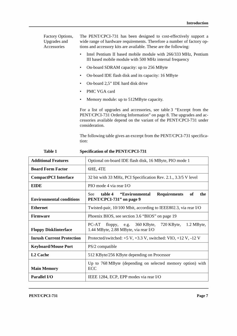
Factory Options, Upgrades and Accessories
The PENT/CPCI-731 has been designed to cost-effectively support awide range of hardware requirements. Therefore a number of factory op-tions and accessory kits are available. These are the following:
• Intel Pentium II based mobile module with 266/333 MHz, PentiuIII based mobile module with 500 MHz internal frequency
• On-board SDRAM capacity: up to 256 MByte
• On-board IDE flash disk and its capacity: 16 MByte
• On-board 2,5” IDE hard disk drive
• PMC VGA card
• Memory module: up to 512MByte capacity.
For a list of upgrades and accessories, see table 3 “Excerpt fromPENT/CPCI-731 Ordering Information” on page 8. The upgrades andcessories available depend on the variant of the PENT/CPCI-731 uconsideration.
The following table gives an excerpt from the PENT/CPCI-731 specifition:
Table 1 Specification of the PENT/CPCI-731
Additional Features Optional on-board IDE flash disk, 16 MByte, PIO mode 1
Board Form Factor 6HE, 4TE
CompactPCI Interface 32 bit with 33 MHz, PCI Specification Rev. 2.1., 3.3/5 V level
EIDE PIO mode 4 via rear I/O
Environmental conditionsSee table 4 “Environmental Requirements of thePENT/CPCI-731” on page 9
Ethernet Twisted-pair, 10/100 Mbit, according to IEEE802.3, via rear I/O
Firmware Phoenix BIOS, see section 3.6 “BIOS” on page 19
Floppy DiskIinterfacePC-AT floppy, e.g. 360 KByte, 720 KByte, 1.2 MByte,1.44 MByte, 2.88 MByte, via rear I/O
Inrush Current Protection Protected/switched: +5 V, +3.3 V, switched: VIO, +12 V, -12 V
Keyboard/Mouse Port PS/2 compatible
L2 Cache 512 KByte/256 KByte depending on Processor
Main MemoryUp to 768 MByte (depending on selected memory option) witECC
Parallel I/O IEEE 1284, ECP, EPP modes via rear I/O
PENT/CPCI-731 Page 7
Introduction
2116
04 1
– 2
May
200
0
e
e
Data Sheets For a list of data sheets see the front matter of this manual.
Ordering Information
Due to the flexible design, the PENT/CPCI-731 is available in severalvariants as well as in several memory and speed options. Consult your lo-cal sales representative to confirm availability of specific combinations.The following table explains the general product nomenclature.
The following table is an excerpt from the PENT/CPCI-731 data sheet.For current information ask your local Force Computers representative.
PMC Slots2 for 32 bit with 33 MHz PMC modules, PCI Specification Rev.2.1, 5 V and 3.3 V level (assembly option)
Power ConsumptionSee table 5 “Typical 5 V and 3.3 V Power Requirements” onpage 10
Processor Pentium II with 266/333 MHz or higher, Pentium III with 500 MHz
Serial I/O 2x, RS232 level, max. rate 115.2 KBaud
USB Port 2x, via rear I/O
Table 1 Specification of the PENT/CPCI-731 (cont.)
Table 2 Product Nomenclature
PENT/CPCI-731/ddd-ppp-Lccc-u
ddd = MByte DRAM
ppp = Processor type
Lccc =2nd level cache
u = MByte IDE flash disk
128 =128 MByte256 =256 MByte
333 =Intel Pentium II333 MHz
L512 =256 KByte
16 = 16MByte
Table 3 Excerpt from the PENT/CPCI-731 Ordering Information
Product Name Description
PENT/CPCI-731/…
…/128-266-L512-0 Intel Pentium II 266 MHz with 128MByte main memory, 512 KByt2nd level cache, no flash disk
…/256-333-L256-16 Intel Pentium II 333 MHz with 256MByte main memory, 256 KByt2nd level cache, 16 MByte flash disk
Page 8 PENT/CPCI-731
Installation
ety
con-
n 3.2
stal-731
3 Installation
Before installing or dismounting the board, refer to section 1 “SafNotes” on page 1.
3.1 Installation Prerequisites and Requirements
Note: Before powering up check the items described in the followinglist.
• Check this section for installation prerequisites and requirements cerning the PENT/CPCI-731
• Check the consistency of the current switch settings (see sectio“Switch Settings” on page 14)
• Check section 3.7 “Upgrades and Accessories” on page 29 for inlation prerequisites and requirements concerning PENT/CPCI-accessories, like e.g. a PMC module
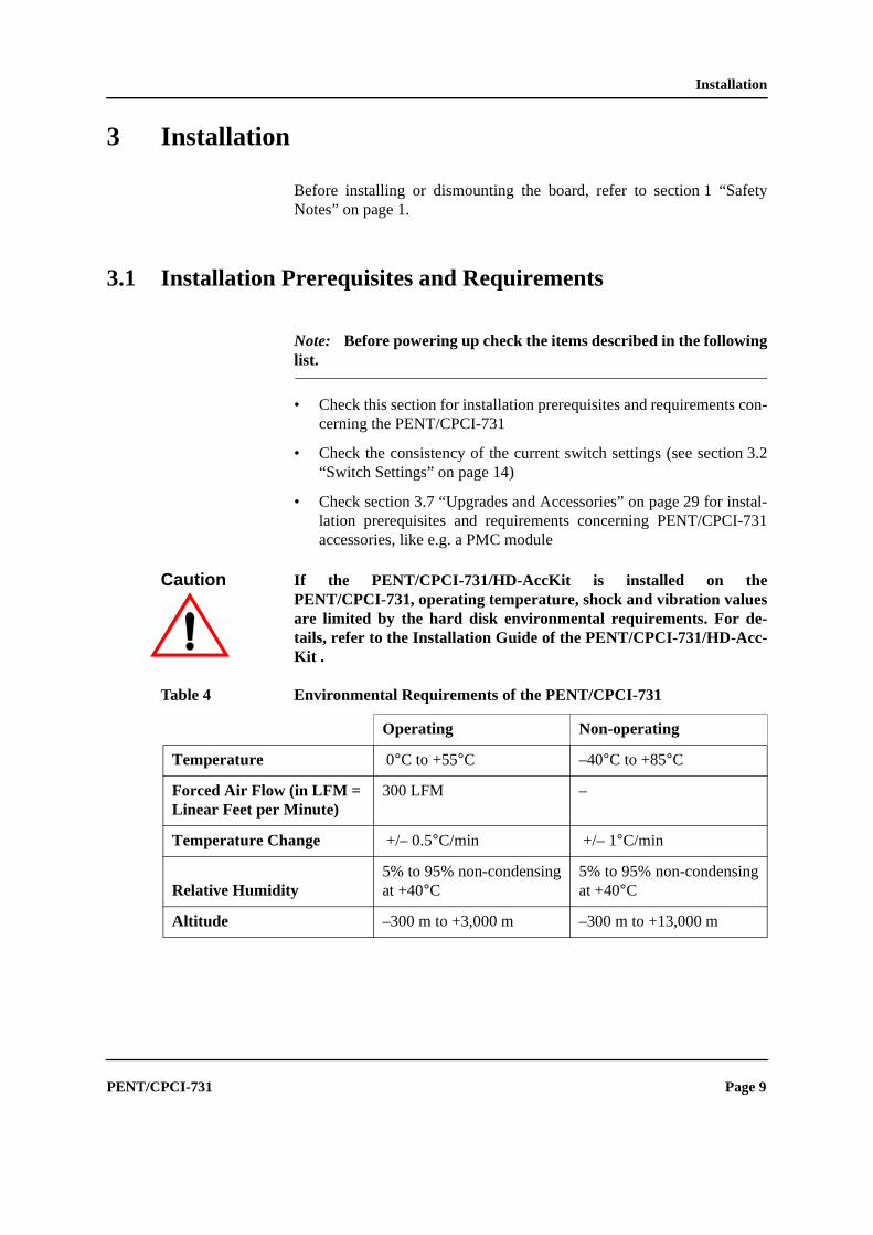
Caution If the PENT/CPCI-731/HD-AccKit is installed on thePENT/CPCI-731, operating temperature, shock and vibration valuesare limited by the hard disk environmental requirements. For de-tails, refer to the Installation Guide of the PENT/CPCI-731/HD-Acc-Kit .
Table 4 Environmental Requirements of the PENT/CPCI-731
Operating Non-operating
Temperature 0°C to +55°C –40°C to +85°C
Forced Air Flow (in LFM = Linear Feet per Minute)
300 LFM –
Temperature Change +/– 0.5°C/min +/– 1°C/min
Relative Humidity5% to 95% non-condensingat +40°C
5% to 95% non-condensingat +40°C
Altitude –300 m to +3,000 m –300 m to +13,000 m
PENT/CPCI-731 Page 9
Installation
2116
04 1
– 2
May
200
0
ulesC
These environmental values must be tested and proven in the used systemconfiguration. These conditions refer to the surroundings of the boardwithin the user environment. Operating temperatures refer to the temper-ature of the air circulating around the board and not to the actual compo-nent temperature. To ensure that the operating conditions are met, forcedair cooling is required within the chassis environment.
Power Requirements
The board’s +/– 12 V power requirements depend on the PMC modinstalled. The PENT/CPCI-731 provides a limited current at the PMsupply pins.
Caution The total maximal power consumption per PMC slot at +/–12 V, 5 V,and 3.3 V level must not exceed 7.5 W (total over-all used voltages).
Typical 5 V and 3.3 V power requirements of the PENT/CPCI-731 aregiven in the following table:
Keyboard, Mouse, USB
Make sure that the lengths of the keyboard/mouse cable and of the USBcable do not exceed 3m each and that the two cables are installed apartfrom other cables.
Floppy Disk Connector
The floppy disk connector is assembled to provide BIOS field upgradeability of the PENT/CPCI-731 if no IOBP-CPCI-731 is available.
Vibration
10 to 15 Hz
15 to 150 Hz
2 mm amplitude2 g
5 mm amplitude5 g
Shock 5 g/11 ms halfsine 15 g/11 ms halfsine
Free Fall100 mm/3 axis 1,200 mm/all edges and
corners (packed state)
Table 4 Environmental Requirements of the PENT/CPCI-731 (cont.)
Operating Non-operating
Table 5 Typical 5 V and 3.3 V Power Requirements
PENT/CPCI-731 (no Memory Board, PMC Mod-ule Installed)
+5 V +3.3 V
PENT/CPCI-731/256-333-L256-16 1.8 A 1.7 A
Page 10 PENT/CPCI-731
Installation
ectedby,o a
ary
g:
behis
enu.6.1n
toBP-
tedd de-ling
heSet-
rima-therW1-ter-
IDE Devices The PENT/CPCI-731 provides a primary and a secondary IDE interfacefor connecting up to four IDE devices. An on-board flash disk may beprovided at the primary IDE interface as a factory option (see below). Ahard disk can be connected to the primary IDE port via the on-board con-nector using the PENT/CPCI-731/HD-AccKit. If two devices are con-nected to an IDE interface, one device has to be the master, the other hasto be the slave. If only one drive is connected to an IDE interface, that de-vice must be set as master.
Due to the nature of IDE some further limitations apply:
• There can be up to three connectors on each ribbon cable connto the primary or secondary PENT/CPCI-731 IDE interface. Thereup to two IDE devices per ribbon cable can be connected tPENT/CPCI-731 IDE interface.
• Never connect more than two devices to the primary or secondPENT/CPCI-731 IDE interface.
• Before connecting IDE devices to an IDE interface, do the followin
– Check for IDE devices already connected to the IDE interface.
– Decide which IDE device should be master and which shouldslave. If only one IDE device is connected to an IDE interface, tdevice must be master.
– Configure the device which you want to connect.
– Ribbon cable length must not exceed 0.45 m (18 inches).
At the first boot after connecting an IDE device use the according min Setup to modify the BIOS parameters appropriately (see section 3“Booting Up and Entering Configuration Utilities (e.g. BIOS Setup)” opage 21 <F2>).
If the PENT/CPCI-731 is provided without on-board flash disk, upfour hard disks can be connected to the PENT/CPCI-731 via the IOCPCI-731 and on-board connector.
IDE Flash Disk (Factory Option)
If the PENT/CPCI-731 is provided with an on-board flash disk connecto its primary IDE interface, a hard disk can be connected as seconvice to the primary IDE interface. This can be done by either assembthe PENT/CPCI-731/HD-AccKit or via an IOBP-CPCI-731 board. Tflash disk can be enabled or disabled via switch SW1-3 (see “Switch tings” on page 14). If the flash disk is enabled and a second device is connected to the pry IDE interface, any of the two devices can be the master while the ois the slave. The flash disk is set to master or slave mode via switch S4. If the flash disk is disabled, the second device at the primary IDE inface must be the master.
PENT/CPCI-731 Page 11
Installation
2116
04 1
– 2
May
200
0
led
hat unin-
ev- de-731),s for
nts.
For the IDE flash disk a data endurance of 300,000 erase/program cyclesper logical sector is guaranteed.
EMC The PENT/CPCI-731 front panel provides two cutouts to enable the in-stallation of PMC modules. If the PENT/CPCI-731 is shipped withoutmodules installed, the front-panel cutouts are covered by blind panels toensure proper EMC shielding.
Note: To ensure proper EMC shielding, check the items describedin the following list.
• Always operate a PENT/CPCI-731:
– With the blind panels for the PENT/CPCI-731 front panel instal
– With the modules installed
• If the PENT/CPCI-731 is upgraded with PMC modules, ensure tthe blind panels are stored in a safe place to be used again whenstalling the upgrades.
Hot Swap The PENT/CPCI-731 provides full Hot Swap functionality. This, hower, does only cover the CPCI interface of connector J1 and J2. If I/Ovices are used at the connectors J3, J4 and J5 (e.g. via IOBP-CPCI-refer to the respective documentation of these signals and interfacehot swap capability.
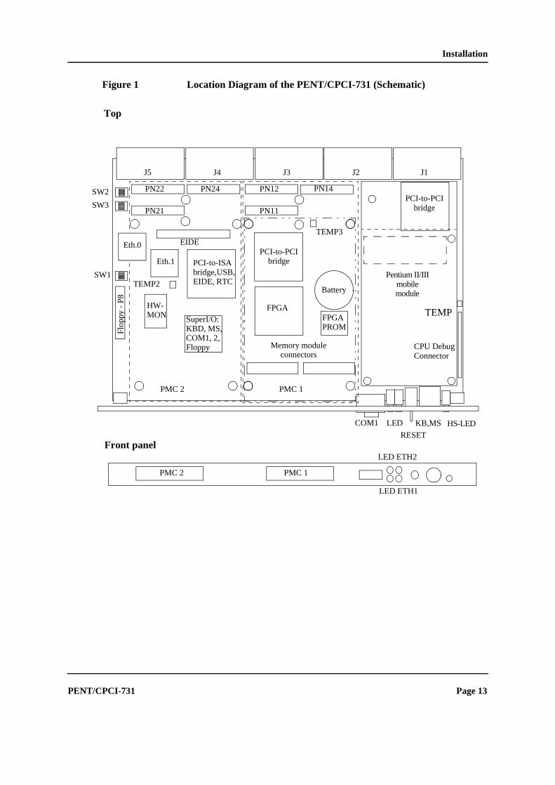
Location Overview
Figure 1 highlights the location of the important base board compone
Page 12 PENT/CPCI-731
Installation
Figure 1 Location Diagram of the PENT/CPCI-731 (Schematic)
Front panel
Top
J2 J1J4J5
PN24 PN12PN22
PN11PN21
SW1
SW3
Battery
PCI-to-PCIbridge
LED
PMC 2 PMC 1
Memory module connectors
Pentium II/III mobilemodule
SuperI/O:KBD, MS,COM1, 2, Floppy
PMC 1PMC 2
LED ETH1
COM1
RESET
TEMP3
TEMP
PN14
HS-LED
FPGA
Flop
py -
P8
SW2
FPGAPROM
J3
KB,MS
TEMP2
EIDEEth.0
Eth.1PCI-to-PCI
bridge
HW-MON
CPU DebugConnector
LED ETH2
PCI-to-ISA bridge,USB, EIDE, RTC
PENT/CPCI-731 Page 13
Installation
2116
04 1
– 2
May
200
0
ic)”
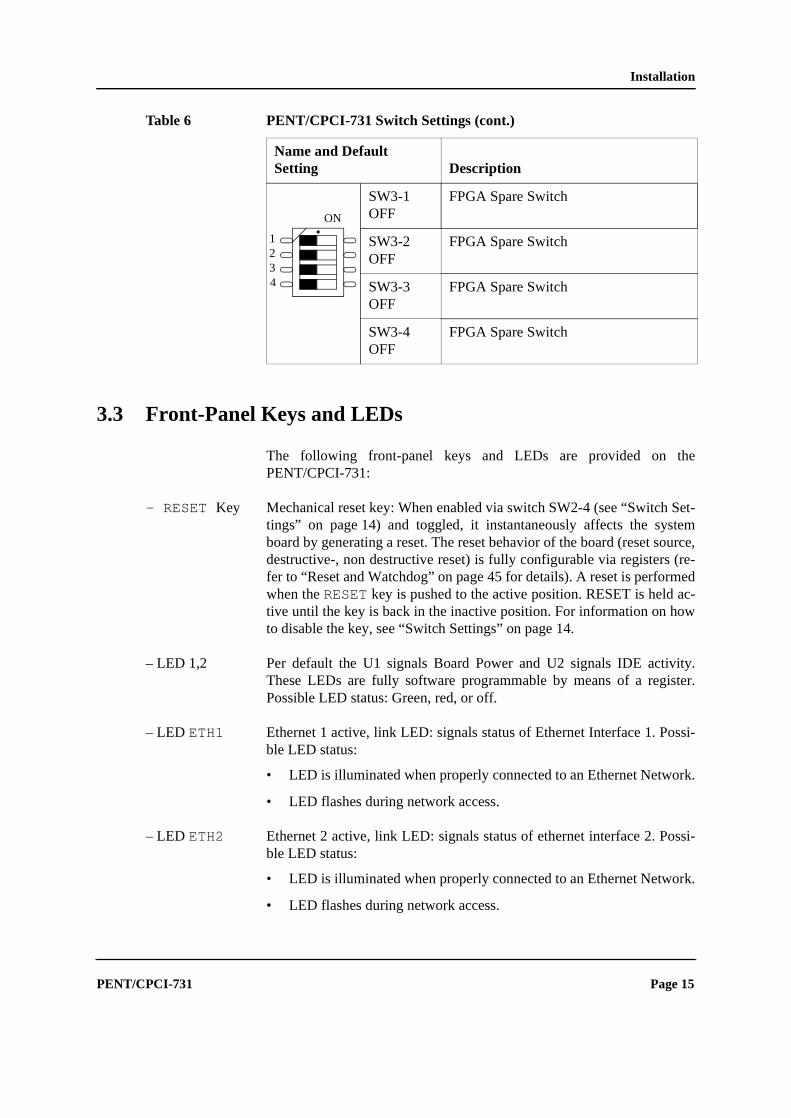
3.2 Switch Settings
The PENT/CPCI-731 is configurable via three micro switches. Theswitches are located on the left-hand side of the base board seen from thefront panel (see “Location Diagram of the PENT/CPCI-731 (Schematon page 13).
Flash disk enable (see “IDE Flash Disk(Factory Option)” on page 11)
= Flash disk disabledON = Flash disk enabled
SW1-4OFF
Flash Disk Master/Slave (boot enable) OFF = Primary IDE slaveON = Primary IDE master
SW2-1OFF
FPGA Download sourceOFF = via EEPROMON = via Download Cable
SW2-2OFF
FPGA Init SelectOFF = Lower 64KB ON = Upper 64KB
SW2-3ON
12V Supervising OFF = EnabledON = Disabled
SW2-4OFF
Reset Key OFF = EnabledON = Disabled
ON
1234
ON
1234
Page 14 PENT/CPCI-731
Installation
Set-tem
ource,(re-medac-ow
vity.ster.
ssi-
rk.
ssi-
rk.
3.3 Front-Panel Keys and LEDs
The following front-panel keys and LEDs are provided on thePENT/CPCI-731:
– RESET Key Mechanical reset key: When enabled via switch SW2-4 (see “Switch tings” on page 14) and toggled, it instantaneously affects the sysboard by generating a reset. The reset behavior of the board (reset sdestructive-, non destructive reset) is fully configurable via registers fer to “Reset and Watchdog” on page 45 for details). A reset is perforwhen the RESET key is pushed to the active position. RESET is held tive until the key is back in the inactive position. For information on hto disable the key, see “Switch Settings” on page 14.
– LED 1,2 Per default the U1 signals Board Power and U2 signals IDE actiThese LEDs are fully software programmable by means of a regiPossible LED status: Green, red, or off.
– LED ETH1 Ethernet 1 active, link LED: signals status of Ethernet Interface 1. Poble LED status:
• LED is illuminated when properly connected to an Ethernet Netwo
• LED flashes during network access.
– LED ETH2 Ethernet 2 active, link LED: signals status of ethernet interface 2. Poble LED status:
• LED is illuminated when properly connected to an Ethernet Netwo
• LED flashes during network access.
SW3-1OFF
FPGA Spare Switch
SW3-2OFF
FPGA Spare Switch
SW3-3OFF
FPGA Spare Switch
SW3-4OFF
FPGA Spare Switch
Table 6 PENT/CPCI-731 Switch Settings (cont.)
Name and Default Setting Description
ON
1234
PENT/CPCI-731 Page 15
Installation
2116
04 1
– 2
May
200
0
- or
fig-
3.4 Front Panel Connectors
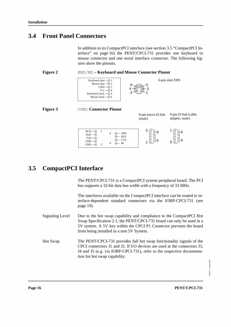
In addition to its CompactPCI interface (see section 3.5 “CompactPCI Interface” on page 16) the PENT/CPCI-731 provides one keyboardmouse connector and one serial interface connector. The followingures show the pinouts.
Figure 2 KBD/MS – Keyboard and Mouse Connector Pinout
Figure 3 COM1 Connector Pinout
3.5 CompactPCI Interface
The PENT/CPCI-731 is a CompactPCI system peripheral board. The PCIbus supports a 32-bit data bus width with a frequency of 33 MHz.
The interfaces available on the CompactPCI interface can be routed to in-terface-dependent standard connectors via the IOBP-CPCI-731 (seepage 19).
Signaling Level Due to the hot swap capability and compliance to the CompactPCI HotSwap Specification 2.1, the PENT/CPCI-731 board can only be used in a5V system. A 5V key within the CPCI P1 Connector prevents the boardfrom being installed in a non 5V System.
Hot Swap The PENT/CPCI-731 provides full hot swap functionality signals of theCPCI connectors J1 and J2. If I/O devices are used at the connectors J3,J4 and J5 (e.g. via IOBP-CPCI-731), refer to the respective documenta-tion for hot swap capability.
6-pin mini DINKeyboard dataMouse data
GNDVcc
Keyboard clockMouse clock
123456
642
53
1
DCDRxDTxDDTRGND
DSRRTSCTSRI
1
5
6
9 1
5
6
9
9-pin D-Sub (cable adapter, male)
9-pin micro D-Sub (male)
1
5
6
9
Page 16 PENT/CPCI-731
Installation
act-iven
J1 and J2 The J1 and J2 connectors implement the CompactPCI 64-bit connectorpinout as specified by the CompactPCI specification. Therefore, thismanual only documents the pinout of the J3, J4 and J5 connectors.
J3 The following interfaces are available via the PENT/CPCI-731 Compact-PCI J3 connector (the designations used in the following pinout are givenin brackets):
• USB 1 (USB1), USB 2 (USB2), COM 1 (COM1), COM 2 (COM2)
• PMC Slot 1 I/O signals (PMC1IO)
Figure 4 CompactPCI J3 Connector Pinout
J4 The following interfaces are available via the PENT/CPCI-731 CompPCI J4 connector (the designations used in the following pinout are gin brackets):
IOBP-CPCI-731 The IOBP-CPCI-731 I/O panel is available as separate price list item forthe PENT/CPCI-731. The I/O panel supports the following interfaces:
• Two Ethernet interfaces
• Keyboard
• Mouse
• Two USB interfaces
• Two serial interfaces
• Two parallel interfaces
• IDE interfaces (primary and secondary)
• Floppy interface
Caution The IOBP-CPCI-731 is especially designed for the base board of thePENT/CPCI-731. Do not use any other I/O panels on thePENT/CPCI-731.
3.6 BIOS
The PENT/CPCI-731 is designed to run with Windows NT Version 4.0host mode. The initial boot-up procedure is performed by BIOS whprovides the following features:
• Plug-and-Play BIOS Specification Version 1.0A compliant (PnP)
• Flexible booting via Multiboot
• Advanced power management
• Two-level password control provided by system security
• Hardware setup via setup program:
– For information on general system configuration via the systBIOS, see section 3.6.1 “Booting Up and Entering ConfiguratiUtilities (e.g. BIOS Setup)” on page 21. Detailed on-line helpavailable for the system BIOS setup.
– For information on option ROMs which may be implemented other boards in the CompactPCI rack, see the respective boardumentation.
Using the setup program BIOS allocates and optimizes resources(memory, interrupts, etc.) for each of the hardware components (vid-eo, disk drives, etc.).
• Hardware initialization at boot: At power-on or reset, BIOS performPower-On Self Test (POST) routines to test system resources. Awards it loads and starts the operating system.
The POST performs the following tasks:
– Run basic and limited RAM test
– Conduct an inventory of the devices installed on the system bo
– Configure hard and floppy disks, keyboard, VGA, serial or paraports
– Configure other devices installed on the system board, CD-ROM drives
– Initialize hardware required for system board features suchplug-and-play and power management
– Run Setup if requested
Page 20 PENT/CPCI-731
Installation
on
nge
ra-
iona theon-n-
ra-forive
oardues
e ask-Set-
3.6.1 Booting Up and Entering Configuration Utilities (e.g. BIOS Setup)
BIOS automatically starts during power up or reset:
<Esc> When pressing <Esc> BIOS continues with the POST screen until theend of POST. It then displays a boot selection menu.For further information, see section 3.6.2 “The Boot Selection Menu”page 22.
<F2> When pressing <F2> BIOS enters Setup.BIOS provides the Setup program to configure the setting of a wide raof system board features. For example:
• LPT, COM1 and COM2 can be remapped via the advanced configution option for integrated peripherals in BIOS Setup.
• The IDE devices can be configured via the main configuratoptions for primary and secondary IDE masters and slaves and viadvanced configuration option for integrated peripherals. This cfiguration capability is used for example at the first boot after conecting an IDE device.
• The floppy type can be configured via the respective main configution options for diskettes. This configuration capability is used example at the first boot after installing a floppy via the respectI/O panel (see note on the IOBP-CPCI-731 on page 19).
Note: If you save the changes you made in Setup, the selections inthe menus are stored in NVRAM (CMOS). The next time the systemboard boots, the BIOS configures the system according to the Setupselections stored in NVRAM (CMOS). If those values cause thesystem boot to fail, reboot and press <F2> to enter Setup. In Setup,you can get the default values or try to change the selections thatcaused the boot to fail. If you get the default values, note that thedisplayed default values are not yet stored to be effective for the nextboot. They are just loaded to be displayed. However, they areeffective when the current boot-up procedure is resumed.
Input Requests If the BIOS or an Option ROM (e.g. of an add-on card) requests keybinput, you are prompted for entering the information. POST continfrom there with the regular POST screen.
POST Error Whenever POST detects a non-fatal error, BIOS displays a messaging you to choose between boot continuation or error correction via up.
PENT/CPCI-731 Page 21
Installation
2116
04 1
– 2
May
200
0
3.6.2 The Boot Selection Menu
The boot selection menu is used to rearrange the boot-order list or to en-ter Setup.
1. In order to override the existing boot sequence (for this boot only)select another boot device from the boot-order list.
If the specified device does not load the operating system, BIOS re-verts to the previous boot sequence.
2. In order to boot via the boot configuration options in Setup, enterSetup and change the device as described in the following section.
3. In order to continue with the previous boot sequence, press <Esc>.
Page 22 PENT/CPCI-731
Installation
3.6.3 Boot Configuration in Setup
The order of the devices from which BIOS attempts to boot the operatingsystem can be selected by the boot configuration options in Setup. DuringPOST, BIOS tries the next one on the list if it is unsuccessful at bootingfrom one device.
Each device listed represents the first of a group of devices if more thanone device of this group is installed on the system. For example, if thereis more than one hard disk drive, the displayed entry represents the firstof such drives as specified in the boot configuration option for fixed me-dia. The same applies to removable media.
The same options determine the order in which POST installs the devicesand the operating system assigns device letters. BIOS supports up to twofloppy devices, to which the operating system may assign, for example,drive letters A: and B:. C:, D:, E:, etc. are assigned to hard-disk drives.
Note: There is not always an exact correspondence between theorder specified in these menus and the letters assigned by theoperating system. Many devices such as legacy Option ROMssupport more than one device, to which can be assigned more thanone letter. If you want the CD-ROM drive to have a letter comingbefore the hard drive, move it in front of the hard drive. The groupof bootable add-in cards refers to devices with non-multiboot-compliant BIOS Option ROM from which you can boot theoperating system.
PENT/CPCI-731 Page 23
Installation
2116
04 1
– 2
May
200
0
Figure 7 A Sample Setup Screen Showing the Boot Configuration Options
In the example above BIOS first attempts to boot in the following order:
Select item to relocate using the UP and DOWN arrow keys. Use the ’+’ and ’-’ keys to move the highlighted boot device up (’+’) or down (’-’) in the priority list
F1 Help ↑↓Select Item -/+ Change Values F9 Setup DefaultsESC Exit ↔Select Menu Enter Select>Sub-Menu F10 Previous Values
Page 24 PENT/CPCI-731
Installation
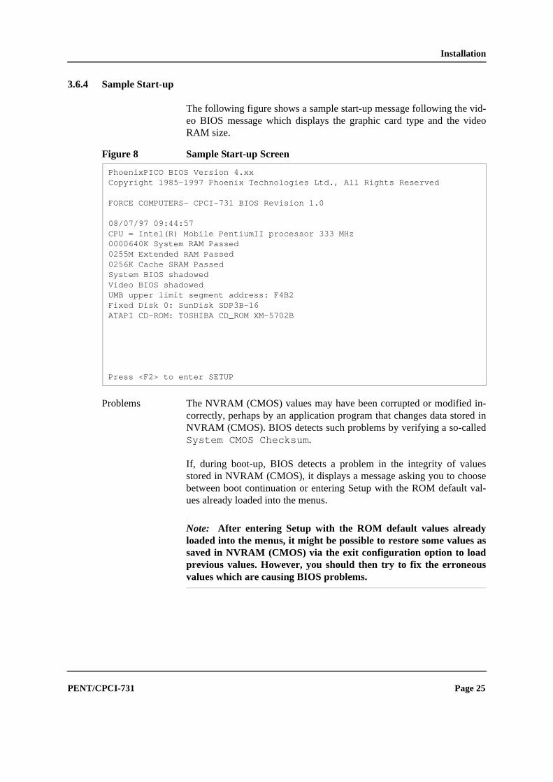
3.6.4 Sample Start-up
The following figure shows a sample start-up message following the vid-eo BIOS message which displays the graphic card type and the videoRAM size.
Figure 8 Sample Start-up Screen
Problems The NVRAM (CMOS) values may have been corrupted or modified in-correctly, perhaps by an application program that changes data stored inNVRAM (CMOS). BIOS detects such problems by verifying a so-calledSystem CMOS Checksum.
If, during boot-up, BIOS detects a problem in the integrity of valuesstored in NVRAM (CMOS), it displays a message asking you to choosebetween boot continuation or entering Setup with the ROM default val-ues already loaded into the menus.
Note: After entering Setup with the ROM default values alreadyloaded into the menus, it might be possible to restore some values assaved in NVRAM (CMOS) via the exit configuration option to loadprevious values. However, you should then try to fix the erroneousvalues which are causing BIOS problems.
PhoenixPICO BIOS Version 4.xxCopyright 1985-1997 Phoenix Technologies Ltd., All Rights Reserved
Note: If your system fails after you made changes in the Setupmenus, you may be able to correct the problem by entering Setupand restoring the original values. If your system displays one of thefollowing messages, write down the message and contact ForceComputers.
• Extended RAM Failed at offset: nnnn
• Failing Bits: nnnn
• Keyboard controller error
• Parity Check 1 nnnn
• Parity Check 2 nnnn
• Real time clock error
• Shadow Ram Failed at offset: nnnn
• System cache error - Cache disabled
• System RAM Failed at offset: nnnn
• System timer error
Message Explanations
nnnn Cache SRAM Passed
nnnn is the amount of system cache in KBytes successfully tested.
CD-ROM Drive Identified
Autotyping identified CD-ROM Drive
Diskette drive A errorDiskette drive B error
Drive A: or B: is present but fails the BIOS POST diskette tests. Chto see that the drive is defined with the proper diskette type in Sand that the diskette drive is attached correctly.
Entering SETUP ...
Starting Setup program.
Extended RAM Failed at offset: nnnn
Extended memory not working or not configured properly at offnnnn.
nnnn Extended RAM Passed
nnnn being the amount of RAM in KBytes successfully tested.
Page 26 PENT/CPCI-731
Installation
Failing Bits: nnnn
The hex number nnnn is a map of the bits at the RAM address (in sys-tem, extended, or shadow memory) which failed the memory test.Each 1 (one) in the map indicates a failed bit.
Fixed Disk 0 FailureFixed Disk 1 FailureFixed Disk Controller Failure
Fixed disk is not working or not configured properly. Check to see iffixed disk is attached properly. Run Setup to be sure the fixed-disktype is correctly identified.
Fixed Disk 0...3 Identified
Autotyping identified specified fixed disk.
Incorrect Drive A type - run SETUPIncorrect Drive B type - run SETUP
Type of floppy drive not correctly identified in Setup.
Invalid NVRAM media type
Problem with NVRAM (CMOS) access.
Keyboard controller error
The keyboard controller failed test. You may have to replace the key-board.
Keyboard error
Keyboard not working.
Keyboard error nn
BIOS discovered a stuck key and displays the scan code nn for thestuck key.
Keyboard locked - Unlock key switch
Unlock the system to proceed.
Monitor type does not match CMOS - Run SETUP
Monitor type not correctly identified in Setup.
Operating system not found
Operating system cannot be located on either drive A: or drive C:. En-ter Setup and see if fixed disk and drive A: are properly identified.
Parity Check 1 nnnn
Parity error found in the system bus. BIOS attempts to locate the ad-dress nnnn and display it on the screen. If it cannot locate the address, itdisplays ????.
Parity Check 2 nnnn
Parity error found in the I/O bus. BIOS attempts to locate the addressnnnn and display it on the screen. If it cannot locate the address, it dis-plays ????.
Press <F1> to resume, <F2> to Setup
Displayed after any recoverable error message. Press <F1> to start theboot process or <F2> to enter Setup and change any settings.
PENT/CPCI-731 Page 27
Installation
2116
04 1
– 2
May
200
0
Previous boot incomplete - Default configuration used
Previous POST did not complete successfully. POST loads default val-ues and offers to run Setup. If the failure was caused by incorrect val-ues and they are not corrected, the next boot is likely to fail. Onsystems with control of wait states, improper Setup settings can alsoterminate POST and cause this error on the next boot. Run Setup andverify that the wait-state configuration is correct. This error is clearedthe next time the system is booted.
Real time clock error
Real-time clock fails BIOS test. May require board repair.
Resource allocation conflict on motherboard - Run Configuration Utility
Run ISA or EISA Configuration Utility to resolve resource conflict.
Shadow Ram Failed at offset: nnnn
Shadow RAM failed at offset nnnn of the 64k block at which the errorwas detected.
nnnn Shadow RAM Passed
nnnn being the amount of shadow RAM in KBytes successfully tested.
System BIOS shadowed
System BIOS copied to shadow RAM.
System cache error - Cache disabled
RAM cache failed the BIOS test. BIOS disabled the cache.
System CMOS checksum bad - run SETUP
System NVRAM (CMOS) has been corrupted or modified incorrectly,perhaps by an application program that changes data stored inNVRAM (CMOS). Run Setup and reconfigure the system either bygetting the Default Values and/or making your own selections.
System RAM Failed at offset: nnnn
System RAM failed at offset nnnn in the 64k block at which the errorwas detected.
nnnn System RAM Passed
Where nnnn is the amount of system RAM in KBytes successfully test-ed.
System timer error
The timer test failed. Requires repair of system board.
UMB upper limit segment address: nnnn
Displays the address nnnn of the upper limit of upper memory blocks,indicating released segments of the BIOS which may be reclaimed by avirtual memory manager.
Video BIOS shadowed
Video BIOS successfully copied to shadow RAM.
Page 28 PENT/CPCI-731
Installation
ront-ule
thisd-
ront-ayForon
oryheoryorya-
in-asside
ctPCI thening
be
to-
Invalid System Configuration Data – run configuration utility
Enter Setup and use the advanced configuration option to reset the con-figuration data (due to corrupted ESCD data).
3.7 Upgrades and Accessories
Apart from the extensions which are possible via the CompactPCI sys-tem, the PENT/CPCI-731 itself allows for an easy and cost-efficient wayto adapt the board to the application’s needs.
PMC Slot 1 The PMC slot 1 can be used to install a standard PMC module with fpanel I/O and rear I/O onto the PENT/CPCI-731. The memory modoption can only be installed on this location if no PMC is required on slot. For further information, see section 3.7.1 “Installing a PMC Moule” on page 31.
PMC Slot 2 The PMC slot 2 can be used to install a standard PMC module with fpanel I/O and rear I/O onto the PENT/CPCI-731. A 2.5’’ hard drive mbe installed at the location of PMC slot 2 instead of a PMC Module. further information, see section 3.7.1 “Installing a PMC Module” page 31.
Memory Module In addition to the local SDRAM of the PENT/CPCI-731 the memmodule PENT/MEM-700 with SDRAM chips can be installed on tPENT/CPCI-731. The maximum possible memory size of the memmodule is 512 MByte. This allows a maximum possible system memof 768 MByte in total. For installation information, refer to the Installtion Guide delivered together with the memory module.
HD-AccKit The IDE hard disk accessory kit PENT/CPCI-731/HD-AccKit can be stalled on PMC slot 2 of the PENT/CPCI-731 providing a local mstorage device. For installation information refer to the Installation Gudelivered together with the accessory kit.
IOBP-CPCI-731 The IOBP-CPCI-731 provides access to the base board’s Compauser I/O interfaces via industry standard connectors. It is included inrear I/O panel accessory kit for PENT/CPCI-731 base boards, contaithe I/O panel itself and the cables.
VGA-AccKit The VGA accessory kit PMC/VGA is a PMC based VGA card. It can installed in one of the PMC slots of the PENT/CPCI-731. For installation information refer to the Installation Guide delivered gether with the VGA accessory kit.
PENT/CPCI-731 Page 29
Installation
2116
04 1
– 2
May
200
0
BIOS-UpKit The BIOS upgrade kit PENT/CPCI-731/BIOS-UpKit contains a DOS-formatted floppy disk with a BIOS upgrade file and upgrade utilities e.g.to reflect extended hardware support. For installation information refer tothe README file contained on the floppy disk.
Page 30 PENT/CPCI-731
Installation
lesidthC
lotsrds,
on- the
14-
our
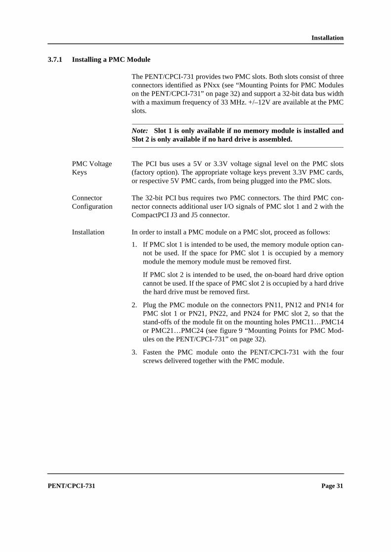
3.7.1 Installing a PMC Module
The PENT/CPCI-731 provides two PMC slots. Both slots consist of threeconnectors identified as PNxx (see “Mounting Points for PMC Moduon the PENT/CPCI-731” on page 32) and support a 32-bit data bus wwith a maximum frequency of 33 MHz. +/–12V are available at the PMslots.
Note: Slot 1 is only available if no memory module is installed andSlot 2 is only available if no hard drive is assembled.
PMC Voltage Keys
The PCI bus uses a 5V or 3.3V voltage signal level on the PMC s(factory option). The appropriate voltage keys prevent 3.3V PMC caor respective 5V PMC cards, from being plugged into the PMC slots.
Connector Configuration
The 32-bit PCI bus requires two PMC connectors. The third PMC cnector connects additional user I/O signals of PMC slot 1 and 2 withCompactPCI J3 and J5 connector.
Installation In order to install a PMC module on a PMC slot, proceed as follows:
1. If PMC slot 1 is intended to be used, the memory module option can-not be used. If the space for PMC slot 1 is occupied by a memorymodule the memory module must be removed first.
If PMC slot 2 is intended to be used, the on-board hard drive optioncannot be used. If the space of PMC slot 2 is occupied by a hard drivethe hard drive must be removed first.
2. Plug the PMC module on the connectors PN11, PN12 and PN14 forPMC slot 1 or PN21, PN22, and PN24 for PMC slot 2, so that thestand-offs of the module fit on the mounting holes PMC11…PMCor PMC21…PMC24 (see figure 9 “Mounting Points for PMC Modules on the PENT/CPCI-731” on page 32).
3. Fasten the PMC module onto the PENT/CPCI-731 with the fscrews delivered together with the PMC module.
PENT/CPCI-731 Page 31
Installation
2116
04 1
– 2
May
200
0
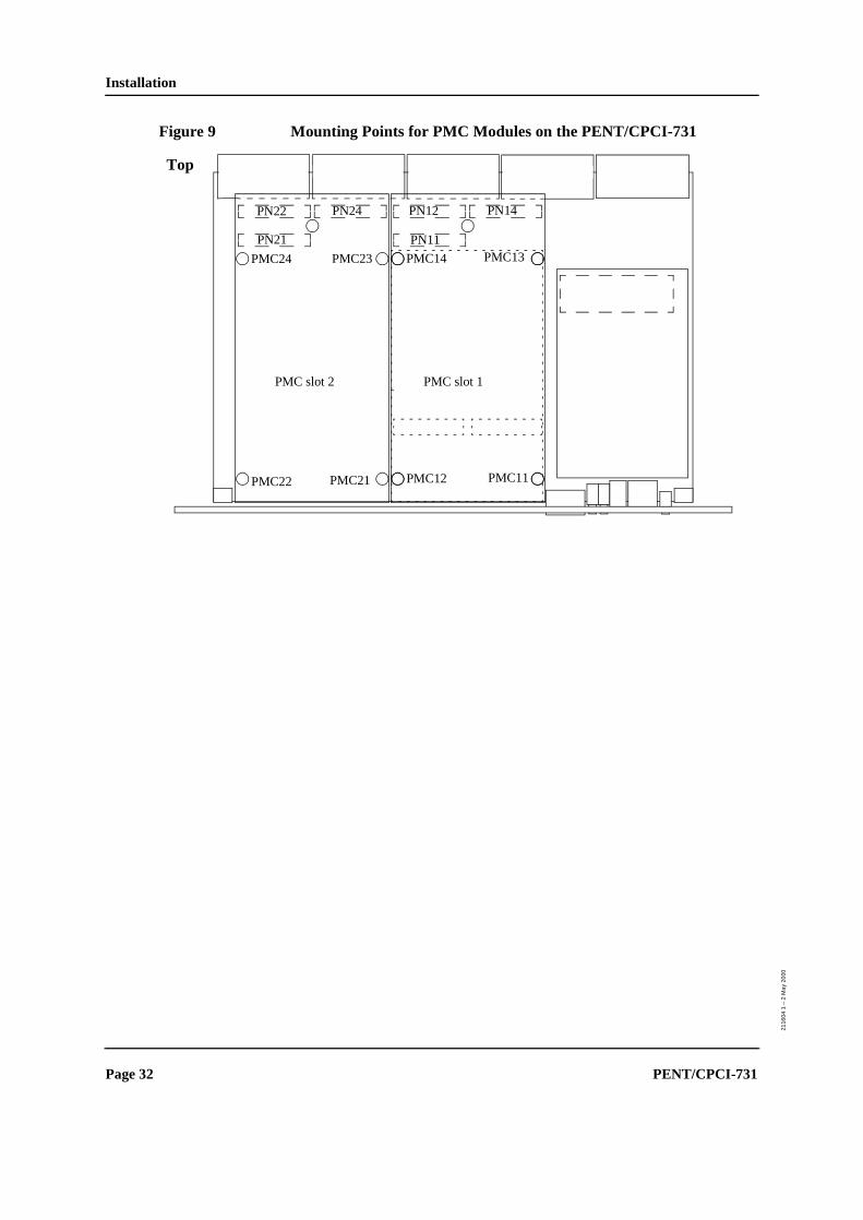
Figure 9 Mounting Points for PMC Modules on the PENT/CPCI-731
PMC13PMC14
PMC11PMC12PMC22 PMC21
PMC24 PMC23
PMC slot 1PMC slot 2
PN12
PN11
PN24PN22
PN21
Top
PN14
Page 32 PENT/CPCI-731
Hardware
s anduc-ow
at the r of
esall
4 Hardware
The PENT/CPCI-731 is a high performance CompactPCI platform. TheI/O board is based on:
• Intel Pentium II/III Mobile Module
• PCI bus with 33 MHz clock frequency
Device Information
Wherever applicable, the PENT/CPCI-731 uses standard PC devicerelated software to implement the features listed in section 2 “Introdtion” on page 5. The following block diagram gives an overview on hthose devices work together and which data paths they use.
Data Sheets It is assumed that the PENT/CPCI-731 is integrated into systemsoperating system level. Therefore, no data sheets are provided in thisRef-erence Guide. For a list of applicable data sheets, see the front mattethis manual.
Board Specific Registers
Following the block diagram for the PENT/CPCI-731, this section givan overview on the I/O and memory maps and describes PENT/CPCI-731 specific registers.
0100 16…010F16 (x) PENT/CPCI-731-specific registers (partially imple-mented in separate FPGA)
00A016…00BF16 x Interrupt controller 2
00C016…00DF16 x DMA controller 2
00E016…00FF16 n.a. Coprocessor
0170 16…017716 x Secondary EIDE / ATAPI
01F016…01F716 x Primary EIDE / ATAPI
0295 16…029616 n.a. Hardware monitor
02F816…02FF16 x COM2
03BC16…03BF16 x LPT1
03C016…03DA16 n.a. Graphic controller
03F216…03F716 x Floppy-EIDE / ATAPI
03F816…03FF16 x COM1
PENT/CPCI-731 Page 35
Hardware
2116
04 1
– 2
May
200
0
Figure 11 Memory Map
System BIOS
Extended memory(depending on actual size,
on PENT/CPCI-731 at most 256 MByte SDRAM)
System BIOS extension
System BIOS
System BIOS extension
4 GByteFFFF.FFFF16
4 GByte – 64 KByteFFFE.FFFF16
4 GByte – 960KByteFFEF.FFFF16
1 MByte000F.FFFF16
1 MByte – 64 KByte000E.FFFF16
Extension BIOS(e.g. for SCSI BIOS and
Ethernet BIOS)
Video (VGA) BIOS
1 MByte – 128 KByte000D.FFFF16
1 MByte – 224 KByte000C.7FFF16
1 MByte – 256 KByte000B.FFFF16
Video memory1 MByte – 384 KByte0009.FFFF16
System memory(first 640 KByte of SDRAM)
IRQ vector table1 KByte0000.03FF16
0000.000016
Page 36 PENT/CPCI-731
Hardware
4.1 I2C-BUS
The PENT/CPCI-731 contains three serial busses which use the I2C serialprotocol. Via these serial busses the CPU can access board status sensors(temperature, voltages), memory sizes etc.
4.1.1 Module Information I2C Bus
The PENT/CPCI-731 contains a serial EEPROM free for applications.The EEPROM has a size of 256 bytes.
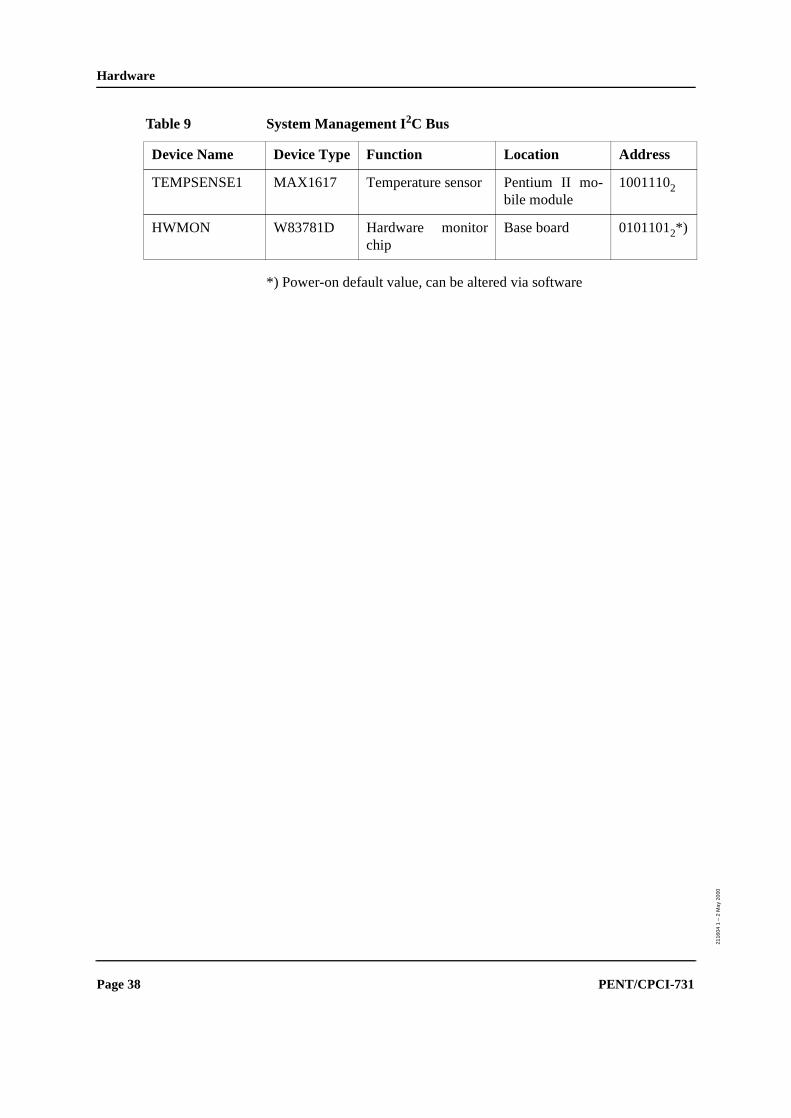
4.1.2 System Management I2C Bus
This serial bus is used for the PC compatible serial devices which complywith the SBus specification from Intel. The bus contains the temperaturesensor on the Pentium II/III Mobile Module, the hardware monitor chipW83781D, 1 SPD serial EEPROM for the first and second memory bank.If the memory module is installed, two SPD serial EEPROMs on themodule are visible on this bus as well. They contain information formemory banks 2 to 5. The SPD serial EEPROMs are built with the 24C02version.
Table 8 Module Information I2C bus
Device Name Device Type Function Location Address
Reserved 24C04 Reserved Base board 10100002
24C02 Memory module 10100112
MEEPROM3 24C02 Free for applications Base board 10100102
Table 9 System Management I2C Bus
Device Name Device Type Function Location Address
SPDEEPROM1 24C02 Memory bank 0, 1 information
Base board 10100002
SPDEEPROM2 24C02 Memory bank 2, 3 information
Memory module 10100012
SPDEEPROM3 24C02 Memory bank 4, 5 information
Memory module 10100102
PENT/CPCI-731 Page 37
Hardware
2116
04 1
– 2
May
200
0
*) Power-on default value, can be altered via software
TEMPSENSE1 MAX1617 Temperature sensor Pentium II mo-bile module
10011102
HWMON W83781D Hardware monitorchip
Base board 01011012*)
Table 9 System Management I2C Bus
Device Name Device Type Function Location Address
Page 38 PENT/CPCI-731
Hardware
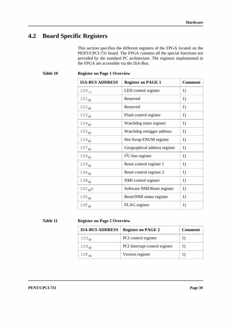
4.2 Board Specific Registers
This section specifies the different registers of the FPGA located on thePENT/CPCI-731 board. The FPGA contains all the special functions notprovided by the standard PC architecture. The registers implemented inthe FPGA are accessible via the ISA-Bus.
Table 10 Register on Page 1 Overview
ISA-BUS ADDRESS Register on PAGE 1 Comment
10016 LED control register 1)
10116 Reserved 1)
10216 Reserved 1)
10316 Flash control register 1)
10416 Watchdog timer register 1)
10516 Watchdog retrigger address 1)
10616 Hot Swap ENUM register 1)
10716 Geographical address register 1)
10816 I2C-bus register 1)
10916 Reset control register 1 1)
10A16 Reset control register 2 1)
10B16 NMI control register 1)
10C16h Software NMI/Reset register 1)
10D16 Reset/NMI status register 1)
10F16 FLAG register 1)
Table 11 Register on Page 2 Overview
ISA-BUS ADDRESS Register on PAGE 2 Comment
10316 PCI control register 1)
10416 PCI Interrupt control register 1)
10F16 Version register 1)
PENT/CPCI-731 Page 39
Hardware
2116
04 1
– 2
May
200
0
gs”
1) Register controlled by the lock feature and locked after power up.2) Register is not controlled by the lock feature.
4.2.1 ISA-BUS Decoding
This section gives a description on how ISA bus decoding is performed.
4.2.1.1 BIOS/User Flash Paging
The PCI-to-ISA bridge provides a 512 KByte or a 1 MByte address win-dow to access the BIOS on the ISA-BUS.
The FPGA allows the mapping of eight pages with a size of 512 KByte orfour pages with a size of 1 MByte in the BIOS address range. Four1 MByte flash devices are provided. The flash device selection is per-formed via register bits in the flash control register (page 40). The ad-dress range is determined with the register bit RANGE.
The following figure gives an overview on the address mapping:
Figure 12 Flash Device Address Mapping
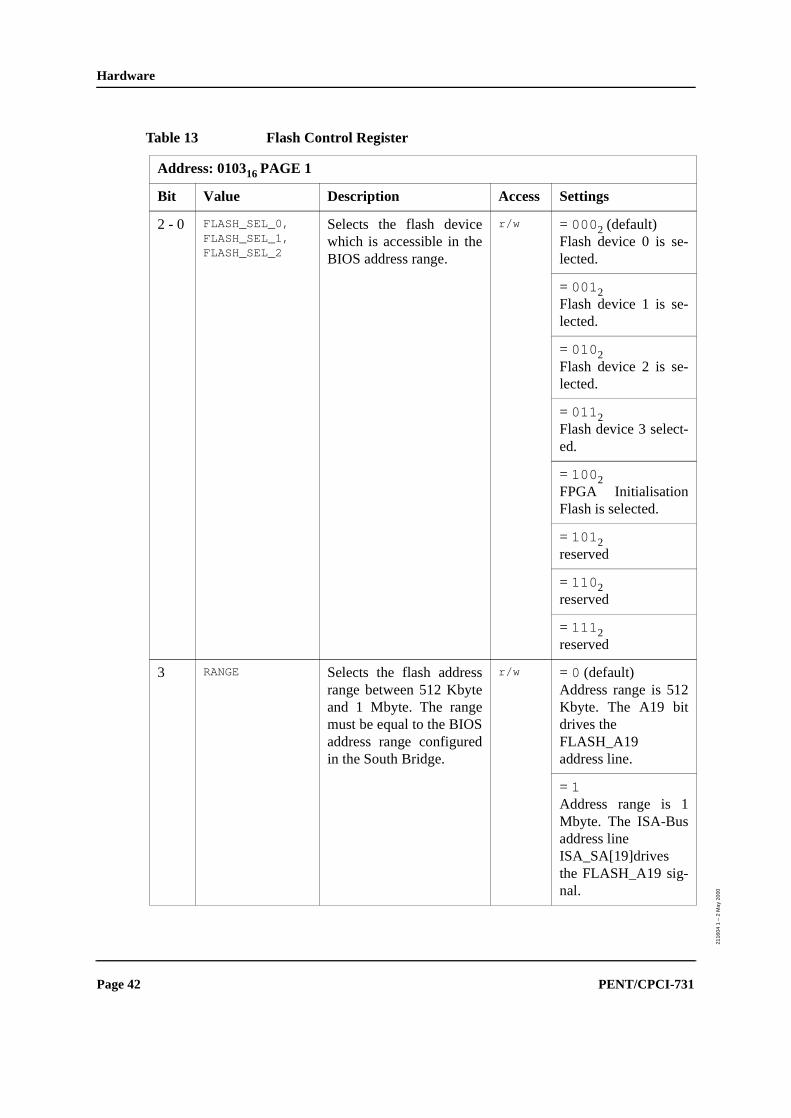
4.2.1.2 Flash Control Register
The flash control register provides the following:
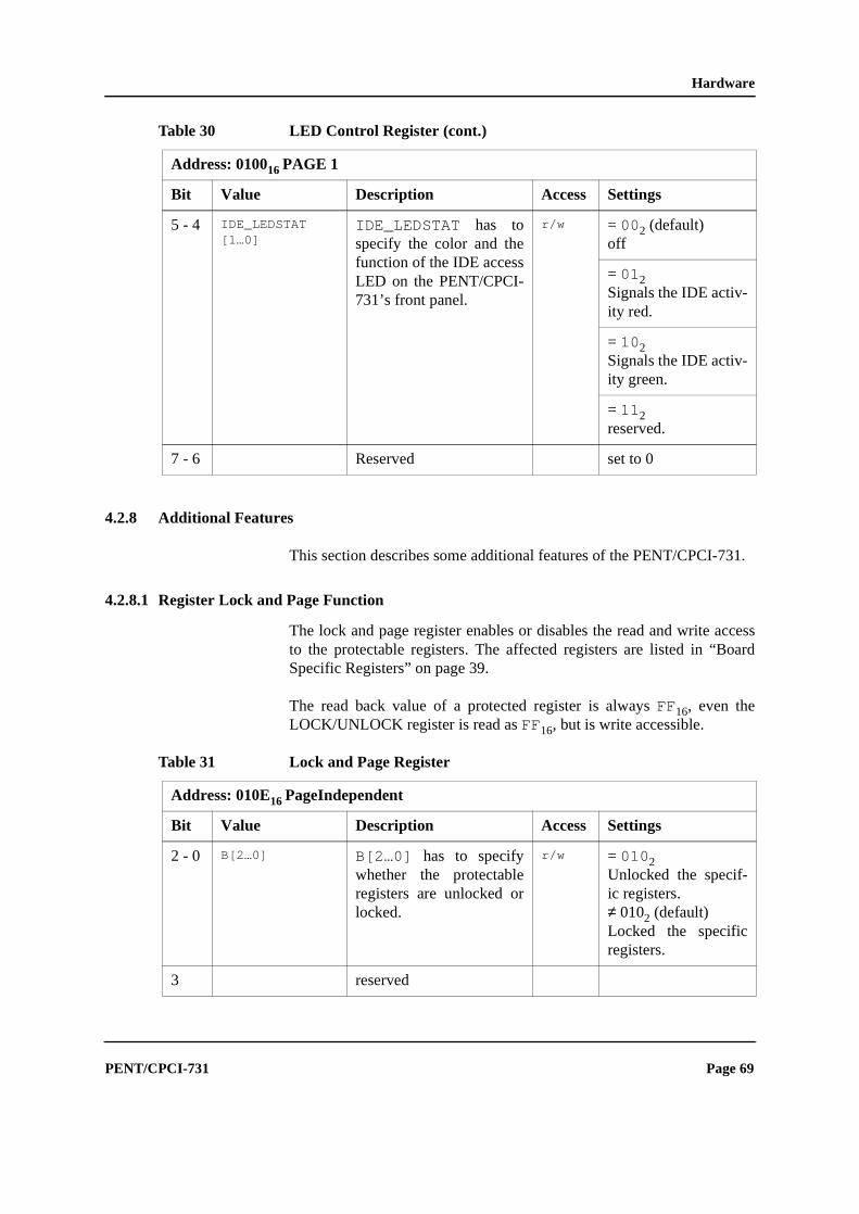
Boot Block Write Protection
The flash device 0 programmed with the standard PC BIOS contains awriteprotected boot block area. The write protection can be enabled/dis-abled via switch SW1-2 (see table 6 “PENT/CPCI-731 Switch Settinon page 14).
Table 12 Independent Register Overview 3
ISA-BUS ADDRESS Register Independent of Page Comment
Selects the flash devicewhich is accessible in theBIOS address range.
r/w = 0002 (default)Flash device 0 is se-lected.
= 0012Flash device 1 is se-lected.
= 0102Flash device 2 is se-lected.
= 0112Flash device 3 select-ed.
= 1002FPGA InitialisationFlash is selected.
= 1012reserved
= 1102reserved
= 1112reserved
3 RANGE Selects the flash addressrange between 512 Kbyteand 1 Mbyte. The rangemust be equal to the BIOSaddress range configuredin the South Bridge.
r/w = 0 (default)Address range is 512Kbyte. The A19 bitdrives theFLASH_A19address line.
= 1Address range is 1Mbyte. The ISA-Busaddress lineISA_SA[19]drivesthe FLASH_A19 sig-nal.
Page 42 PENT/CPCI-731
Hardware
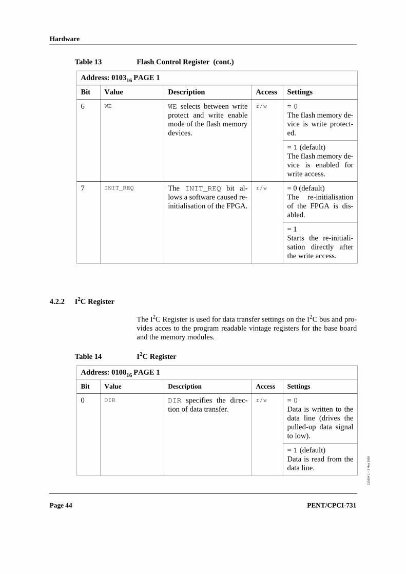
4 A19 The A19 bit drives theaddress line FLASH_A19of the selected flash de-vices directly and deter-mines the 512 Kbyte page.If the RANGE bit is set to1, the A19 bit has nofunction anymore and theFLASH_A19 is driven bythe ISA-Bus address lineISA_SA[19].
r/w = 0The flash address lineFLASH_A19 is driv-en low. The button512 Kbyte page ofone 1 Mbyte deviceis selected. The se-lected pages are 1, 3,5, 7; depending on thesetting of theFLASH_SEL[2…0]bits.
= 1 (default)The flash address lineFLASH_A19 is driv-en high. The top 512Kbyte page of one1 Mbyte device is se-lected. The selectedpages are 0, 2, 4, 6;depending on the set-ting of theFLASH_SEL[2…0]bits.
5 A20 The A20 bit drives the ad-dress line FLASH_A20 ofthe flash devices directly.This bit has no functionfor using one Mbyte flashdevice.
r/w = 0The flash address lineFLASH_A20 is driv-en low.
= 1 (default)The flash address lineFLASH_A20 is driv-en high.
Table 13 Flash Control Register (cont.)
Address: 010316 PAGE 1
Bit Value Description Access Settings
PENT/CPCI-731 Page 43
Hardware
2116
04 1
– 2
May
200
0
4.2.2 I2C Register
The I2C Register is used for data transfer settings on the I2C bus and pro-vides acces to the program readable vintage registers for the base boardand the memory modules.
6 WE WE selects between writeprotect and write enablemode of the flash memorydevices.
r/w = 0 The flash memory de-vice is write protect-ed.
= 1 (default)The flash memory de-vice is enabled forwrite access.
7 INIT_REQ The INIT_REQ bit al-lows a software caused re-initialisation of the FPGA.
r/w = 0 (default)The re-initialisationof the FPGA is dis-abled.
= 1Starts the re-initiali-sation directly afterthe write access.
Table 13 Flash Control Register (cont.)
Address: 010316 PAGE 1
Bit Value Description Access Settings
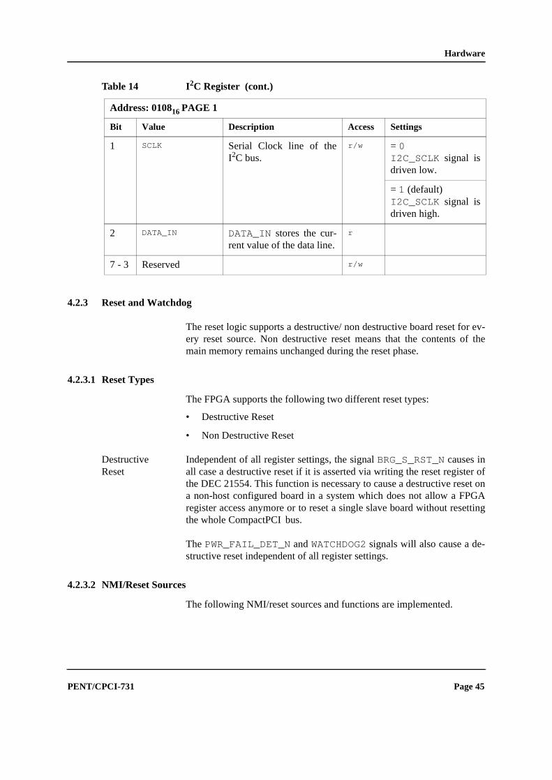
Table 14 I2C Register
Address: 010816 PAGE 1
Bit Value Description Access Settings
0 DIR DIR specifies the direc-tion of data transfer.
r/w = 0Data is written to thedata line (drives thepulled-up data signalto low).
= 1 (default)Data is read from thedata line.
Page 44 PENT/CPCI-731
Hardware
er ofet onGA
etting
-
4.2.3 Reset and Watchdog
The reset logic supports a destructive/ non destructive board reset for ev-ery reset source. Non destructive reset means that the contents of themain memory remains unchanged during the reset phase.
4.2.3.1 Reset Types
The FPGA supports the following two different reset types:
• Destructive Reset
• Non Destructive Reset
Destructive Reset
Independent of all register settings, the signal BRG_S_RST_N causes inall case a destructive reset if it is asserted via writing the reset registthe DEC 21554. This function is necessary to cause a destructive resa non-host configured board in a system which does not allow a FPregister access anymore or to reset a single slave board without resthe whole CompactPCI bus.
The PWR_FAIL_DET_N and WATCHDOG2 signals will also cause a destructive reset independent of all register settings.
4.2.3.2 NMI/Reset Sources
The following NMI/reset sources and functions are implemented.
1 SCLK Serial Clock line of theI2C bus.
r/w = 0I2C_SCLK signal isdriven low.
= 1 (default)I2C_SCLK signal isdriven high.
2 DATA_IN DATA_IN stores the cur-rent value of the data line.
r
7 - 3 Reserved r/w
Table 14 I2C Register (cont.)
Address: 010816 PAGE 1
Bit Value Description Access Settings
PENT/CPCI-731 Page 45
Hardware
2116
04 1
– 2
May
200
0
be
truc-
dis-
• In the Reset control register 1 the NMI/reset sources canenabled/disabled to cause a reset.
• The Reset control register 2 determines the reset type (destive/non destructive).
• In the NMI control register, the NMI/reset source can be enabled/abled to cause an NMI.
Table 15 NMI/Reset Sources
Signal Name Function
Reset Maskable
Reset Type
NMI Maskable Comments
Destructive
Non Destructive
CPCI_RST_N CompactPCI bus re-set
x x x x Externalsource,bidirectional
CPCI_PBRST_N
CompactPCI buspush button reset
x x x x External source
RESET_IN_P5 Reset input from P5 x x x x
SWITCH_RESET_N
Frontpanel reset key x x x x
BRG_S_RST_N
This signal is con-trolled by the RE-SET register of thePCI-to-PCI bridge.
- x - - External sourc-es, causes inany cases a de-structive reset
PWR_FAIL_DET_N
Power fail detectionform power up CPLD
- x - -
WDOG_1_N Watchdog 1 x x x x Internal source
WDOG_2_N Watchdog 2 x x - -
SOFT Software x x x x
SB PCI-to-ISA bridge NA NA NA - Externalsource, causesonly a NMI
RST_HW_MON_N
System control chip NA NA NA x Externalsource, causesonly a NMI
Page 46 PENT/CPCI-731
Hardware
-
e
4.2.3.3 Reset Control Register 1
Table 16 Possible NMI/Reset Configurations
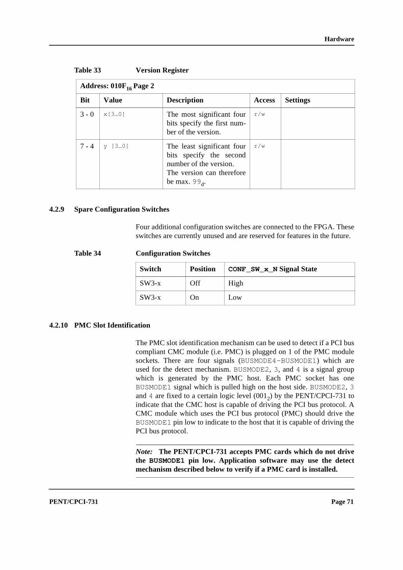
Reset Mask Bit
(Reset Configuration Register 1)
Reset Type Bit
(Reset Configuration Register 2)
NMI Mask Bit
(NMI Configuration Register) NMI/Reset Source
1 Don’t care 1 disabLed
0 0 1 Causes a destructive reset (default)
0 1 1 causes a non destructive reset
1 Don’t care 0 Causes a NMI
0 0 0 Causes a NMI and after 1s a destructive reset
0 1 0 Causes a NMI and after 1s a non destructivreset
Table 17 Reset Control Register 1
Address: 010916 PAGE 1
Bit Value Description Access Settings
0 SWITCH_RST_MASK
Reset mask bit for thefront-panel reset key
r/w = 0 (default)The reset source isenabled.
= 1 The reset source isdisabled.
1 RST_IN_P5_MASK
Reset mask bit for the re-set input from the P5 con-nector
r/w = 0 (default)The reset source isenabled.
= 1 The reset source isdisabled.
PENT/CPCI-731 Page 47
Hardware
2116
04 1
– 2
May
200
0
Note: Invalid configuration if WDOG2_RST_MASK is enabled andWDOG1_RST_MASK is disabled.
2 CPCI_PBRST_MASK
Reset mask bit forCompactPCI buspush buttom reset.
r/w = 0 (default)The reset source isenabled.
= 1 The reset source isdisabled.
3 CPCI_RST_MASK
Reset mask bit for theCompactPCI bus Reset.
r/w = 0 (default)The reset source isenabled.
= 1 The reset source isdisabled.
4 WDOG1_RST_MASK
Reset mask bit for thewatchdog 1 reset.
r/w = 0 The reset source isenabled.
= 1 (default)The reset source isdisabled.
5 SOFT_RST_MASK
Reset mask bit for thesoftware reset.
r/w = 0 (default)The reset source isenabled.
= 1 The reset source isdisabled.
6 WDOG2_RST_MASK
Reset mask bit for thewatchdog 2 reset.
r/w = 0 The reset source isenabled.
= 1 (default)The reset source isdisabled.
7 Reserved
Table 17 Reset Control Register 1 (cont.)
Address: 010916 PAGE 1
Bit Value Description Access Settings
Page 48 PENT/CPCI-731
Hardware
4.2.3.4 Reset Control Register 2
Table 18 Reset Control Register 2
Address: 010A16 PAGE 1
Bit Value Description Access Settings
0 SWITCH_RST_TYPE
Specifies the reset type ofthe reset key.
r/w = 0 (default)The reset sourcecauses a destructivereset.
= 1 The reset sourcecauses a non destruc-tive reset.
1 RST_IN_P5_TYPE
Specifies the reset type ofthe reset input from the P5connector.
r/w = 0 (default)The reset sourcecauses a destructivereset.
= 1 The reset sourcecauses a non destruc-tive reset.
2 CPCI_PBRST_TYPE
Specifies the reset type ofthe CompactPCI bus pushbutton reset.
r/w = 0 (default)The reset sourcecauses a destructivereset.
= 1 The reset sourcecauses a non destruc-tive reset.
3 CPCI_RST_TYPE
Specifies the reset type ofthe CompactPCI bus reset.
r/w = 0 (default)The reset sourcecauses a destructivereset.
= 1 The reset sourcecauses a non destruc-tive reset.
PENT/CPCI-731 Page 49
Hardware
2116
04 1
– 2
May
200
0
4.2.3.5 Non Maskable Interrupt NMI
Every reset source is configured via the NMI control register to cause anNMI before asserting the reset signals. In addition to the described resetsources, the PCI-to-ISA bridge and the Hardware Monitor Chip may alsocause an NMI. The PCI-to-ISA bridge NMI source is not maskable in theNMI control register. The time between the assertion of the CPU_NMIsignal and the reset signals is fixed to 1 s.
5 - 4 WDOG1_RST_TYPE_0, WDOG1_RST_TYPE_1
Specifies the reset type ofwatchdog reset.
r/w = 002 (default)The reset sourcecauses a destructivereset.= 012The reset sourcecauses a non destruc-tive reset.= 102The reset sourcecauses a NMI.= 112reserved.
6 SOFT_RST_TYPE
Specifies the reset type ofthe software reset.
r/w = 0 (default)The reset sourcecauses a destructivereset.
= 1 The reset sourcecauses a non destruc-tive reset.
7 Reserved
Table 18 Reset Control Register 2 (cont.)
Address: 010A16 PAGE 1
Bit Value Description Access Settings
Page 50 PENT/CPCI-731
Hardware
4.2.3.6 NMI Control Register
Table 19 NMI Control Register
Address: 010B16 PAGE 1
Bit Value Description Access Settings
0 SWITCH_NMI_MASK
NMI mask bit for the resetkey.
r/w = 0 NMI is enabled.
= 1 (default)NMI is disabled.
1 RST_IN_P5_NMI_MASK
NMI mask bit for the resetinput of the P5 connector.
r/w = 0 NMI is enabled.
= 1 (default)NMI is disabled.
2 CPCI_PB_NMI_MASK
NMI mask bit for theCompactPCI bus pushbutton reset.
r/w = 0 NMI is enabled.
= 1 (default)NMI is disabled.
3 CPCI_NMI_MASK
NMI mask bit for theCompactPCI bus reset.
r/w = 0 NMI is enabled.
= 1 (default)NMI is disabled.
4 WDOG_NMI_MASK
NMI mask bit for thewatchdog.Note:These settings overridethe reset control register 2.If the NMI is disabledhere no NMI will be gen-erated even if bits 4 and 5of the reset control regis-ter are programmed to002.
r/w = 0 NMI is enabled.
= 1 (default)NMI is disabled.
5 SOFT_NMI_MASK
NMI mask bit for the soft-ware reset.
r/w = 0 NMI is enabled.
= 1 (default)NMI is disabled.
PENT/CPCI-731 Page 51
Hardware
2116
04 1
– 2
May
200
0
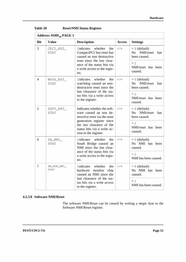
4.2.3.7 Reset/NMI Status Register
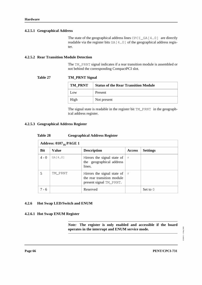
The Reset/NMI Status register allows the software to find out, what kindof reset source has been caused a NMI and/or a non-destructive reset andenables clearing all of its status bits via a write access to this register.
6 HW_MON_NMI_MASK
NMI mask bit for theHardware Monitor Chipreset.
r/w = 0 NMI is enabled.
= 1 (default)NMI is disabled.
7 Reserved
Table 19 NMI Control Register (cont.)
Address: 010B16 PAGE 1
Bit Value Description Access Settings
Table 20 Reset/NMI Status Register
Address: 010D16 PAGE 1
Bit Value Description Access Settings
0 SWITCH_RST_STAT Indicates whether the re-set key has caused anNMI and/or reset since thelast clearance of the sta-tus bits via a write accessto the register.
r/w = 0 (default)No NMI/reset hasbeen caused.
= 1 NMI/reset has beencaused.
1 RST_IN_P5_RST_STAT
Indicates whether the re-set input of the P5 connec-tor has caused anNMI/reset since the lastclearance of the status bitsvia a write access to theregister.
r/w = 0 (default)No NMI/reset hasbeen caused.
= 1 NMI/reset has beencaused.
2 CPCI_PBRST_STAT Indicates whether theCompactPCI bus pushbutton reset caused anNMI/reset since the lastclearance of the status bitsvia a write access to theregister.
r/w = 0 (default)No NMI/reset hasbeen caused.
= 1 NMI/reset has beencaused.
Page 52 PENT/CPCI-731
Hardware
4.2.3.8 Software NMI/Reset
The software NMI/Reset can be caused by writing a magic byte to theSoftware NMI/Reset register.
3 CPCI_RST_STAT
Indicates whether theCompactPCI bus reset hascaused an non destructivereset since the last clear-ance of the status bits viaa write access to the regis-ter.
r/w = 0 (default)No NMI/reset hasbeen caused.
= 1 NMI/reset has beencaused.
4 WDOG_RST_STAT
Indicates whether thewatchdog caused an non-destructive reset since thelast clearance of the sta-tus bits via a write accessto the register.
r/w = 0 (default)No NMI/reset hasbeen caused.
= 1NMI/reset has beencaused.
5 SOFT_RST_STAT
Indicates whether the soft-ware caused an non de-structive reset via the resetgeneration register sincethe last clearance of thestatus bits via a write ac-cess to the register.
r/w = 0 (default)No NMI/reset hasbeen caused.
= 1 NMI/reset has beencaused.
6 SB_NMI_STAT
Indicates whether theSouth Bridge caused anNMI since the last clear-ance of the status bits viaa write access to the regis-ter.
r/w = 0 (default)No NMI has beencaused.
= 1 NMI has been caused.
7 HW_MON_NMI_STAT
Indicates whether thehardware monitor chipcaused an NMI since thelast clearance of the sta-tus bits via a write accessto the register.
r/w = 0 (default)No NMI has beencaused.
= 1 NMI has been caused.
Table 20 Reset/NMI Status Register
Address: 010D16 PAGE 1
Bit Value Description Access Settings
PENT/CPCI-731 Page 53
Hardware
2116
04 1
– 2
May
200
0
ibleun-0.sert
timedog
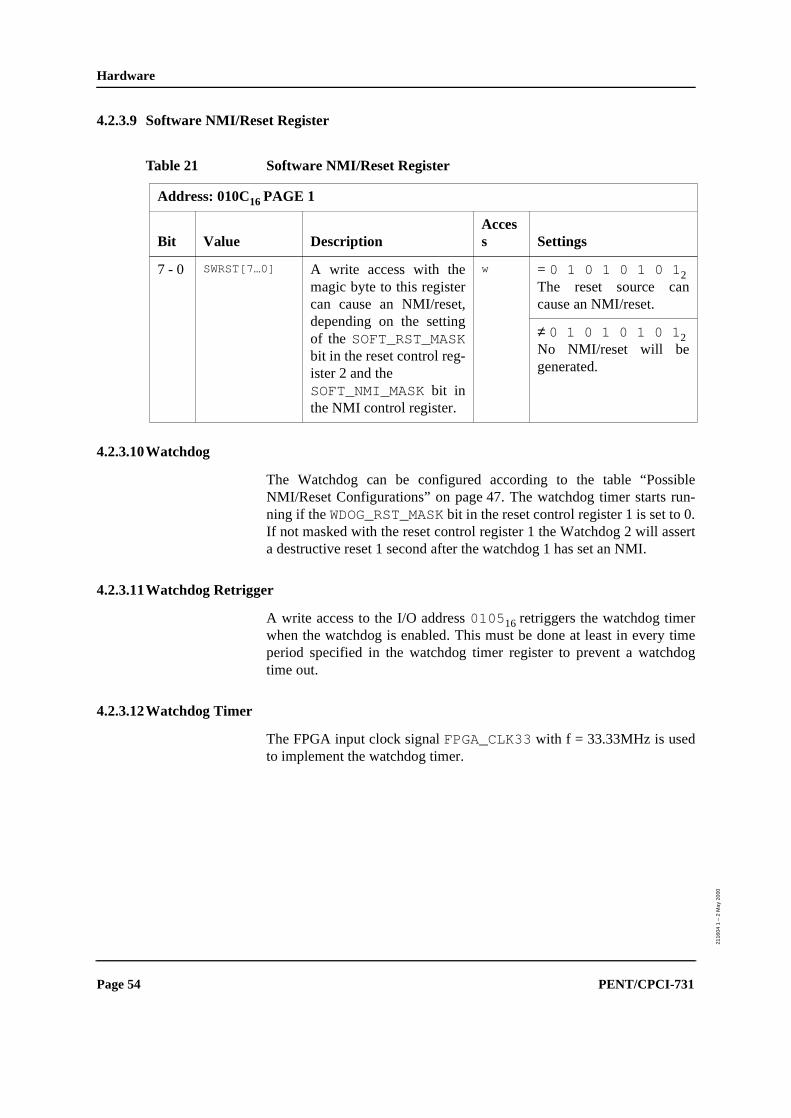
4.2.3.9 Software NMI/Reset Register
4.2.3.10Watchdog
The Watchdog can be configured according to the table “PossNMI/Reset Configurations” on page 47. The watchdog timer starts rning if the WDOG_RST_MASK bit in the reset control register 1 is set to If not masked with the reset control register 1 the Watchdog 2 will asa destructive reset 1 second after the watchdog 1 has set an NMI.
4.2.3.11Watchdog Retrigger
A write access to the I/O address 010516 retriggers the watchdog timerwhen the watchdog is enabled. This must be done at least in everyperiod specified in the watchdog timer register to prevent a watchtime out.
4.2.3.12Watchdog Timer
The FPGA input clock signal FPGA_CLK33 with f = 33.33MHz is usedto implement the watchdog timer.
Table 21 Software NMI/Reset Register
Address: 010C16 PAGE 1
Bit Value DescriptionAccess Settings
7 - 0 SWRST[7…0] A write access with themagic byte to this registercan cause an NMI/reset,depending on the settingof the SOFT_RST_MASKbit in the reset control reg-ister 2 and theSOFT_NMI_MASK bit inthe NMI control register.
w = 0 1 0 1 0 1 0 12The reset source cancause an NMI/reset.
≠ 0 1 0 1 0 1 0 12No NMI/reset will begenerated.
Page 54 PENT/CPCI-731
Hardware
Table 22 Watchdog Timer
DIV [3..0]Bit
(Watchdog Control Register)
FPGA_CLK33 Divider
33,33 Mhz == 30,00 ns Watchdog Timer
00002 213 = 8192 245.760 us
00012 214 = 16384 491.520 us
00102 215 = 32768 983.040 us
00112 216 = 65536 1.966 us
01002 217 = 131072 3.932 ms
01012 218 = 262144 7.864 ms
01102 219 = 524288 15.729 ms
01112 220 = 1048576 31.457 ms
10002 221 = 2097152 62.915 ms
10012 222 = 4194304 0.126 s
10102 223 = 8388608 0.252 s
10112 224 = 16777216 0.503 s
11002 225 = 33554432 1.007 s
11012 226 = 67108864 2.013 s
11102 227 = 134217728 4.027 s
11112 228 = 268435465 8.053 s
PENT/CPCI-731 Page 55
Hardware
2116
04 1
– 2
May
200
0
4.2.3.13Watchdog Timer Register
Table 23 Watchdog Timer Register
Address: 010416 PAGE 1
Bit Value Description Access Settings
3-0 DIV[0…3] Controls the retrigger peri-od of the watchdog. Theretrigger period is pro-grammable from245.760 us to 8.053 s in16 steps.
r/w = 00002== 245.760 us
= 00012== 491.520 us
= 00102== 983.040 us
= 00112== 1.966 ms
= 01002== 3.932 ms
= 01012== 7.864 ms
= 01102== 15.729 ms
= 01112== 31.457 ms
= 10002== 62.915 ms
= 10012== 0.126 s
= 10102== 0.252 s
= 10112== 0.503 s
= 11002== 1.007 s
= 11012== 2.013 s
= 11102== 4.027 s
Page 56 PENT/CPCI-731
Hardware
4.2.4 PCI Configuration and Interrupt, Operating Modes
The PENT/CPCI-731 is configurable to operate in as normal non-host(peripheral) board or in a special mode, the Interrupt and ENUM servicemode.
4.2.4.1 Interrupt and Enum Service Mode
In this mode CompactPCI Interrupts and ENUM signals are serviced andthe CompactPCI reset signal is driven. The interrupt routing is config-urable independent of the currently active mode.
4.2.4.2 Signal Direction
Via the PCI_DIR bit of the PCI control register The PENT/CPCI-731can be configured to cause or to receive CompactPCI interrupts, Com-pactPCI reset and Hot Swap CompactPCI ENUM. The inverted state ofthis bit is mirrored to the INT_LVT_DIR signal to control the directionof the CompactPCI signal buffer on the PENT/CPCI-731.
After power up the CPCI_SYSEN_N signal is sampled and the state iswritten in the PCI_DIR register bit. A low state means that the board isconfigured to provide the interrupt and enum service mode functionalityand a high signal state configures the board to operate as a normal non-host board. The PCI_DIR bit could be overwritten after power up by soft-ware.
= 11112 == 8.053 s
7 -4 Reserved
Table 23 Watchdog Timer Register (cont.)
Address: 010416 PAGE 1
Bit Value Description Access Settings
Table 24 Signal Direction
CompactPCI Signal
Interrupt and Enum Service Mode
Configuration as Non-Host
InterruptsCPCI_INT[D…A]_N
Input Output
PENT/CPCI-731 Page 57
Hardware
2116
04 1
– 2
May
200
0
4.2.4.3 Interrupt Mask
Every CompactPCI Interrupt is maskable via the INTx_MASK bit in thePCI Control register, x = A, B, C, D.
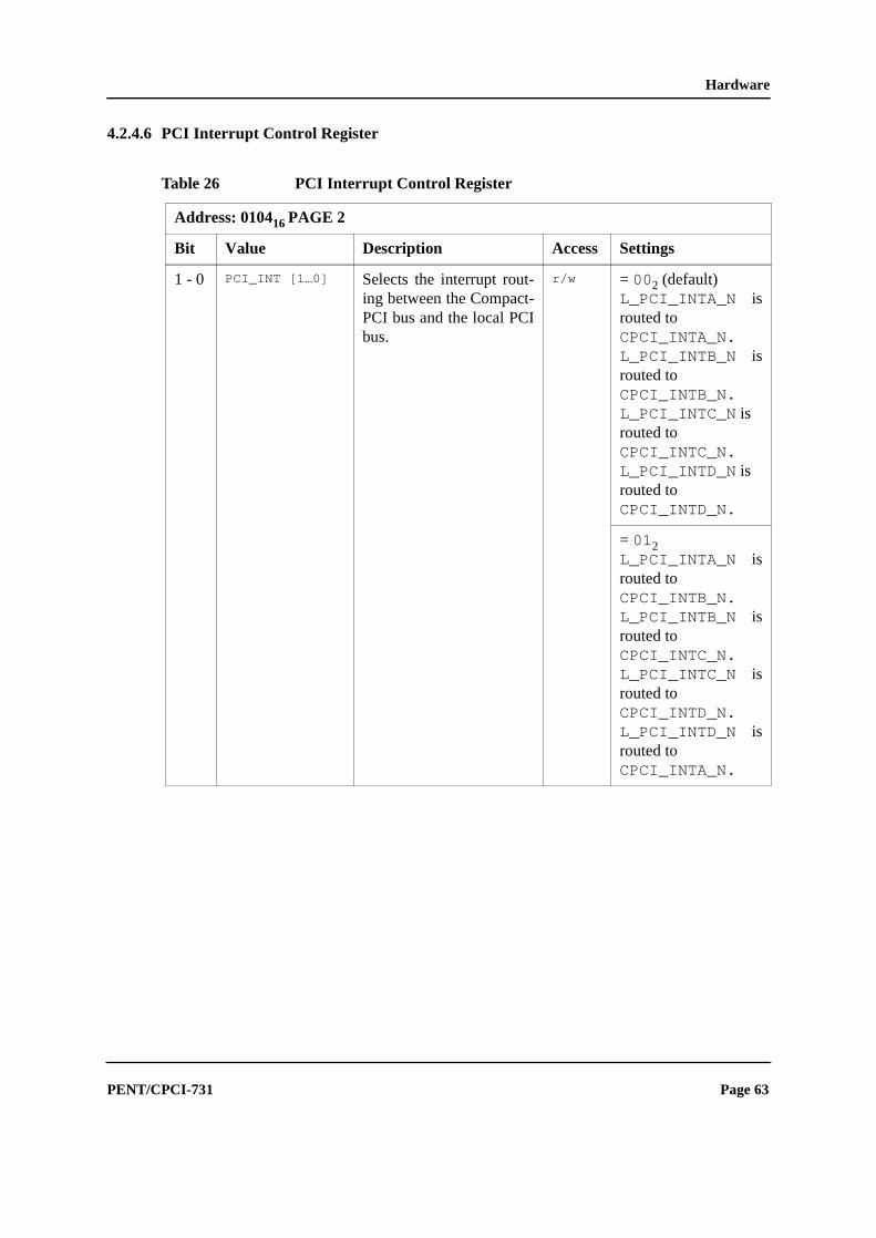
4.2.4.4 Interrupt Routing
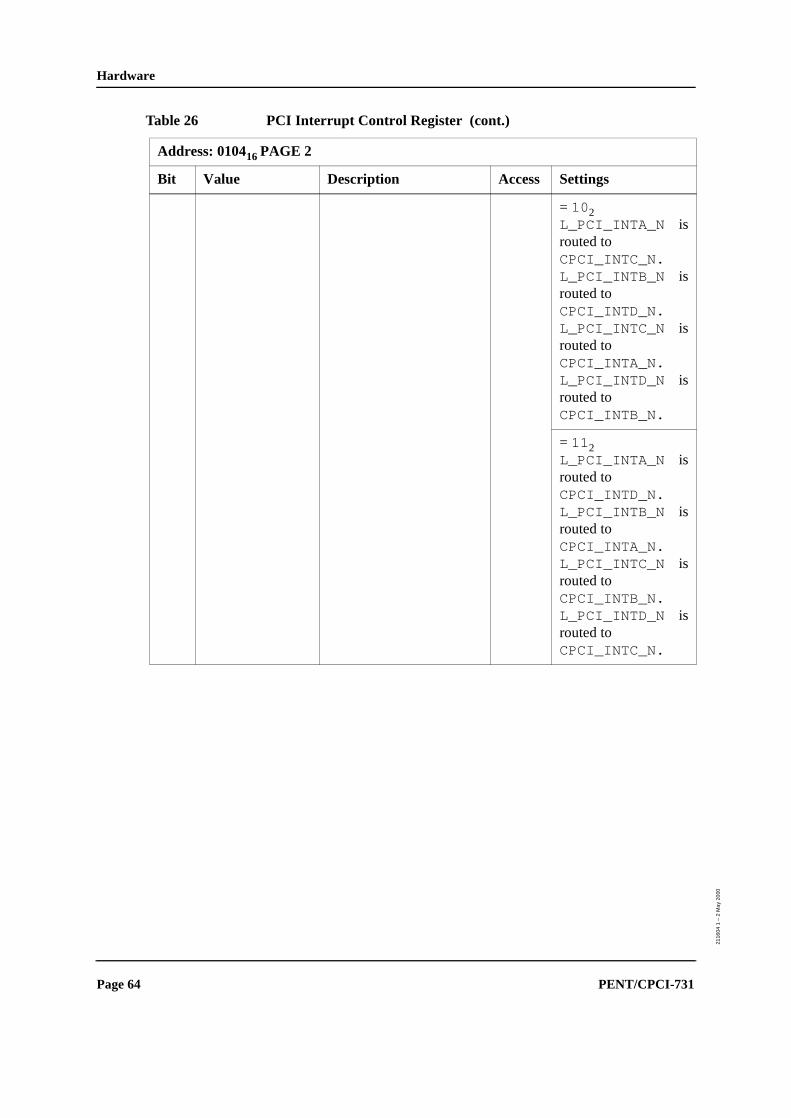
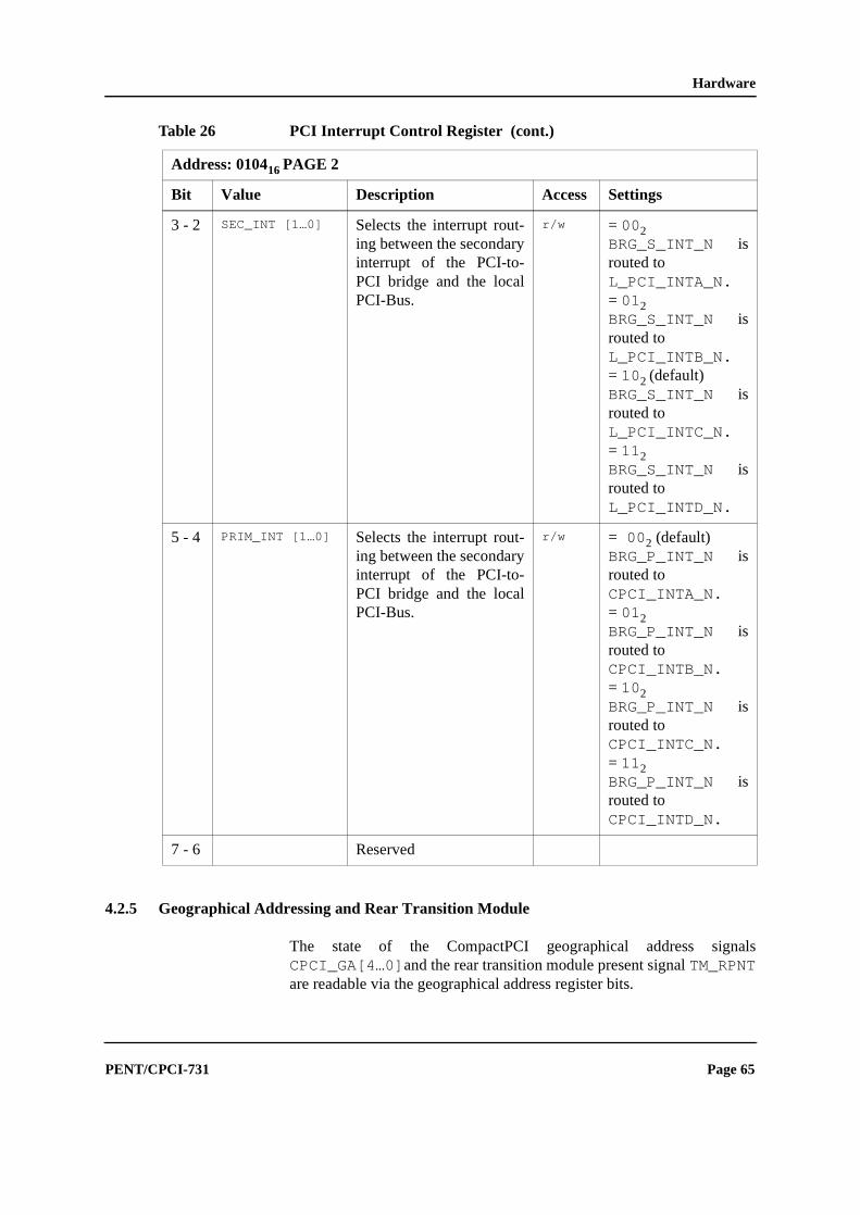
The interrupt routing from the CompactPCI to the local PCI bus, the in-terrupt routing from the primary side of the PCI-to-PCI bridge to theCompactPCI and the interrupt routing from the secondary side of thePCI-to-PCI bridge to the local PCI bus are selectable in the PCI interruptcontrol register.
ResetCPCI_RST_N
Output Input
ENUM CPCI_ENUM_N
Input Output
Table 24 Signal Direction (cont.)
CompactPCI Signal
Interrupt and Enum Service Mode
Configuration as Non-Host
Page 58 PENT/CPCI-731
Hardware
4.2.4.5 PCI Control Register
Table 25 PCI Control Register
Address: 010316 PAGE 2
Bit Value Description Access Settings
0 INTD_MASK The CompactPCI bus in-terrupts are maskable in-dependent of the setting ofthe PCI-Bus direction bitPCI_DIR. This is usefulif more than one board ina system operates in theInterrupt and ENUM ser-vice mode to share the in-terrupt servicing.
By default the non-hostboard drives no interruptsto the CompactPCI back-plane, since the local pro-cessor serves all localinterrupts.
If the board is configuredto use the Interrupt andENUM service mode andis intended to serve inter-rupts the INTx_MASKbits must be set to 0.
r/w = 0 The correspondingCompactPCI bus in-terrupt is not masked(enable).
= 1 (default)The correspondingCompactPCI bus in-terrupt is masked(disabled).
1 INTC_MASK r/w = 0The correspondingCompactPCI bus in-terrupt is not masked(enable).
= 1 (default)The correspondingCompactPCI bus in-terrupt is masked(disabled).
2 INTB_MASK r/w = 0The correspondingCompactPCI bus in-terrupt is not masked(enable).
= 1 (default)The correspondingCompactPCI bus in-terrupt is masked(disabled).
PENT/CPCI-731 Page 59
Hardware
2116
04 1
– 2
May
200
0
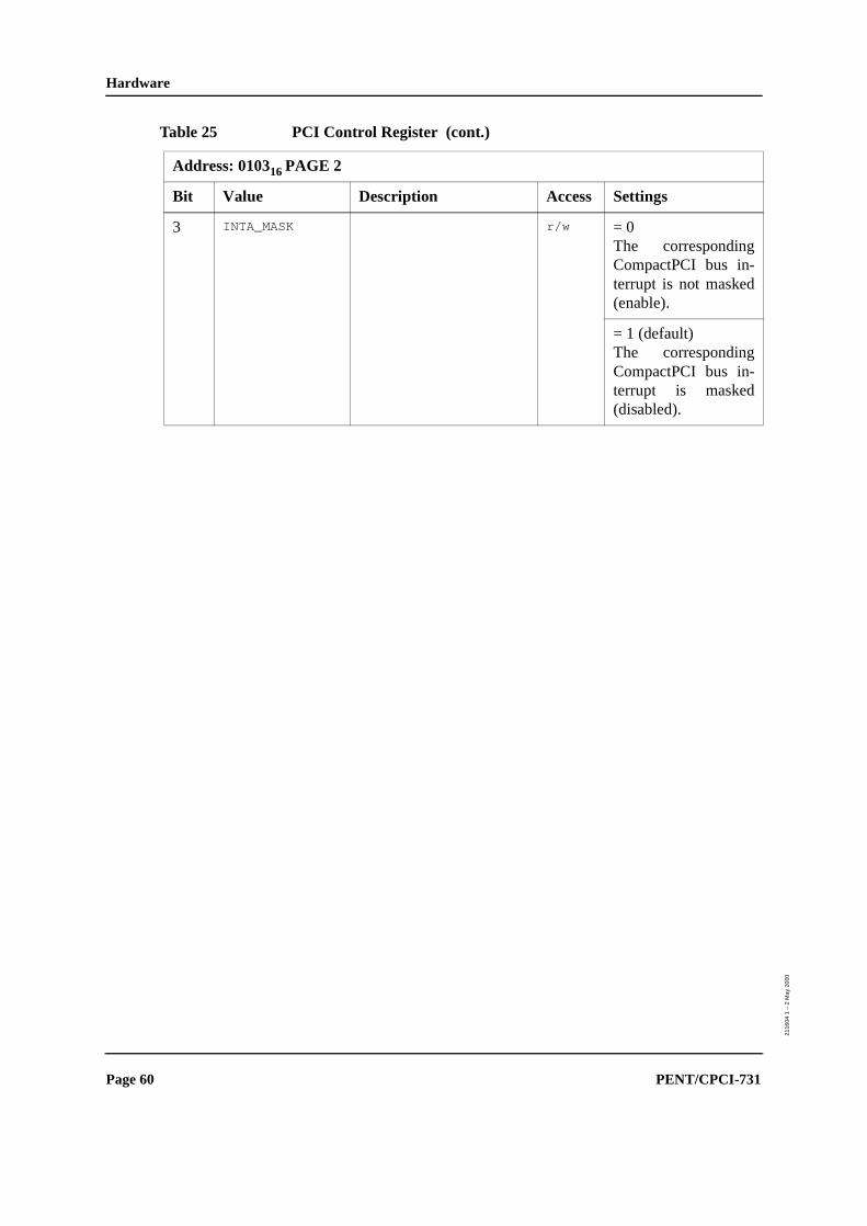
3 INTA_MASK r/w = 0The correspondingCompactPCI bus in-terrupt is not masked(enable).
= 1 (default)The correspondingCompactPCI bus in-terrupt is masked(disabled).
Table 25 PCI Control Register (cont.)
Address: 010316 PAGE 2
Bit Value Description Access Settings
Page 60 PENT/CPCI-731
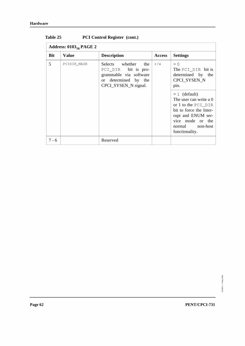
Hardware
4 PCI_DIR Selects the direction of theCompactPCI bus inter-rupt, reset and ENUM sig-nals. The FPGA outputsignal INT_LVT_DIRmirrors the state of thisbit. The bit state afterpower up depends on theCPCI_SYSEN_N signal.After power up this bitcan be overwritten bysoftware to enable the In-terrupt and ENUM servicemode.
r/w = 0 The PENT/CPCI-731provides the Inter-rupt and ENUM ser-vice mode and drivesthe signalINT_LVT_DIR low.TheBRG_ENUM_R_Nsignal of the PCI-to-PCI bridge is maskedand is not visible tothe CompactPCI bus.The Hot SwapENUM register isconfigured to detectthe CPCI_ENUM_Nassertion of otherboards.The CPCI_RST_Nsignal is output.
= 1 (default)The PENT/CPCI-731provides non-hostfunctionality anddrives the signalINT_LVT_DIRhigh.TheBRG_ENUM_R_Nsignal of the PCI-to-PCI bridge is un-masked and is visibleto the CompactPCIbus. The Hot SwapENUM register is dis-abled. The CPCI_RST_Nsignal is input.
Table 25 PCI Control Register (cont.)
Address: 010316 PAGE 2
Bit Value Description Access Settings
PENT/CPCI-731 Page 61
Hardware
2116
04 1
– 2
May
200
0
5 PCIDIR_MASK Selects whether thePCI_DIR bit is pro-grammable via softwareor determined by theCPCI_SYSEN_N signal.
r/w = 0 The PCI_DIR bit isdetermined by theCPCI_SYSEN_Npin.
= 1 (default)The user can write a 0or 1 to the PCI_DIRbit to force the Inter-rupt and ENUM ser-vice mode or thenormal non-hostfunctionality.
7 - 6 Reserved
Table 25 PCI Control Register (cont.)
Address: 010316 PAGE 2
Bit Value Description Access Settings
Page 62 PENT/CPCI-731
Hardware
4.2.4.6 PCI Interrupt Control Register
Table 26 PCI Interrupt Control Register
Address: 010416 PAGE 2
Bit Value Description Access Settings
1 - 0 PCI_INT [1…0] Selects the interrupt rout-ing between the Compact-PCI bus and the local PCIbus.
4.2.5 Geographical Addressing and Rear Transition Module
The state of the CompactPCI geographical address signalsCPCI_GA[4…0]and the rear transition module present signal TM_RPNTare readable via the geographical address register bits.
3 - 2 SEC_INT [1…0] Selects the interrupt rout-ing between the secondaryinterrupt of the PCI-to-PCI bridge and the localPCI-Bus.
The state of the geographical address lines CPCI_GA[4…0] are directlyreadable via the register bits GA[4…0] of the geographical address regis-ter.
4.2.5.2 Rear Transition Module Detection
The TM_PRNT signal indicates if a rear transition module is assembled ornot behind the corresponding CompactPCI slot.
The signal state is readable in the register bit TM_PRNT in the geograph-ical address register.
4.2.5.3 Geographical Address Register
4.2.6 Hot Swap LED/Switch and ENUM
4.2.6.1 Hot Swap ENUM Register
Note: The register is only enabled and accessible if the boardoperates in the interrupt and ENUM service mode.
Table 27 TM_PRNT Signal
TM_PRNT Status of the Rear Transition Module
Low Present
High Not present
Table 28 Geographical Address Register
Address: 010716 PAGE 1
Bit Value Description Access Settings
4 - 0 GA[4…0] Mirrors the signal state ofthe geographical addresslines.
r
5 TM_PRNT Mirrors the signal state ofthe rear transition modulepresent signal TM_PRNT.
r
7 - 6 Reserved Set to 0
Page 66 PENT/CPCI-731
Hardware
The ENUM register has three major functions:
1. Detect the assertion of the CPCI_ENUM_R_N signal caused by othernon-host boards.
2. Mask/unmask the BRG_ENUM_R_N signal from the on-board PCI-to-PCI bridge.
3. Support polling and interrupt mode to detect the assertion of theCPCI_ENUM_R_N signal.
Table 29 Hot Swap ENUM Register
Address: 010616 PAGE 1
Bit Value Description Access Settings
0 ENUM ENUM shows the logic lev-el of theCPCI_ENUM_R_N sig-nal at the CompactPCIbackplane.
r = 0 CPCI_ENUM_R_Nsignal is asserted.
= 1 CPCI_ENUM_R_N isnot asserted.
1 MASK MASK is used to mask theENUM interrupt.
r/w = 0 (default)The ENUM interruptis masked and no in-terrupts will occur.
= 1 The ENUM interruptis unmasked and aninterrupt will occur ifthe ENUM signal onthe CompactPCIbackplane is asserted.
2 IRQ IRQ reflects the status ofthe interrupt line.
r/w = 0 (default)The ISA-Bus IRQ isnot asserted.
= 1 The ISA-Bus IRQlevel 11 is asserted ifthe ENUM signalgoes active and theIRQ stays active un-til a write access tothe register.
7-3 Reserved Set to 0
PENT/CPCI-731 Page 67
Hardware
2116
04 1
– 2
May
200
0
4.2.7 LEDs
The FPGA controls two bicolor (red/green) LEDs. The LEDs are config-urable as user LEDs and/or to show the primary and secondary IDE de-vice access.
The LED 2 can be programmed as IDE-led. User LED 2 has no effect inthat case.
4.2.7.1 LED Control Register
The LED control register specifies the status of the LEDs. The BIOS acti-vates the IDE LED after booting.
Table 30 LED Control Register
Address: 010016 PAGE 1
Bit Value Description Access Settings
1 - 0 1_LEDSTAT [1…0] 1_LEDSTAT has to spec-ify the status of the userLED on the PENT/CPCI-731’s front panel.
r/w = 002 (default)off
= 012red
= 102green
= 112off
3 - 2 2_LEDSTAT [1…0] 2_LEDSTAT has to spec-ify the status of the userLED on the PENT/CPCI-731’s front panel. Thefunction of 2_LEDSTATdepends on the configura-tion of IDE_LEDSTAT.
r/w = 002 (default)off
= 012red
= 102green
= 112off
Page 68 PENT/CPCI-731
Hardware
oard
4.2.8 Additional Features
This section describes some additional features of the PENT/CPCI-731.
4.2.8.1 Register Lock and Page Function
The lock and page register enables or disables the read and write accessto the protectable registers. The affected registers are listed in “BSpecific Registers” on page 39.
The read back value of a protected register is always FF16, even theLOCK/UNLOCK register is read as FF16, but is write accessible.
5 - 4 IDE_LEDSTAT [1…0]
IDE_LEDSTAT has tospecify the color and thefunction of the IDE accessLED on the PENT/CPCI-731’s front panel.
r/w = 002 (default)off
= 012Signals the IDE activ-ity red.
= 102Signals the IDE activ-ity green.
= 112reserved.
7 - 6 Reserved set to 0
Table 30 LED Control Register (cont.)
Address: 010016 PAGE 1
Bit Value Description Access Settings
Table 31 Lock and Page Register
Address: 010E16 PageIndependent
Bit Value Description Access Settings
2 - 0 B[2…0] B[2…0] has to specifywhether the protectableregisters are unlocked orlocked.
r/w = 010 2Unlocked the specif-ic registers.≠ 0102 (default)Locked the specificregisters.
3 reserved
PENT/CPCI-731 Page 69
Hardware
2116
04 1
– 2
May
200
0
4.2.8.2 Version Register
The version register provides the version of the FPGA software in BCD-code.
4 PAGE The PAGE bit sets the ac-cess to the registers locat-ed in PAGE 1 or PAGE 2.
r/w = 0Registers located inPAGE 1 are accessi-ble.
= 1 Registers located inPAGE 2 are accessi-ble.
7 Reserved
Table 31 Lock and Page Register (cont.)
Address: 010E16 PageIndependent
Bit Value Description Access Settings
Table 32 Flag Register
Address: 010F16 Page 1
Bit Value Description Access Settings
0 FLAG BIOS determines whetherit should execute fullPOST or directly jump toan external boot loader lo-cated in a user flash.
r/w = 0Normal BIOS is car-ried out.
= 1 BIOS jumps to an ex-ternal bootloader.
7 - 1 Reserved set to 0
Page 70 PENT/CPCI-731
Hardware
4.2.9 Spare Configuration Switches
Four additional configuration switches are connected to the FPGA. Theseswitches are currently unused and are reserved for features in the future.
4.2.10 PMC Slot Identification
The PMC slot identification mechanism can be used to detect if a PCI buscompliant CMC module (i.e. PMC) is plugged on 1 of the PMC modulesockets. There are four signals (BUSMODE4-BUSMODE1) which areused for the detect mechanism. BUSMODE2, 3, and 4 is a signal groupwhich is generated by the PMC host. Each PMC socket has oneBUSMODE1 signal which is pulled high on the host side. BUSMODE2, 3and 4 are fixed to a certain logic level (0012) by the PENT/CPCI-731 toindicate that the CMC host is capable of driving the PCI bus protocol. ACMC module which uses the PCI bus protocol (PMC) should drive theBUSMODE1 pin low to indicate to the host that it is capable of driving thePCI bus protocol.
Note: The PENT/CPCI-731 accepts PMC cards which do not drivethe BUSMODE1 pin low. Application software may use the detectmechanism described below to verify if a PMC card is installed.
Table 33 Version Register
Address: 010F16 Page 2
Bit Value Description Access Settings
3 - 0 x[3…0] The most significant fourbits specify the first num-ber of the version.
r/w
7 - 4 y [3…0] The least significant fourbits specify the secondnumber of the version.The version can thereforebe max. 99d.
r/w
Table 34 Configuration Switches
Switch Position CONF_SW_x_N Signal State
SW3-x Off High
SW3-x On Low
PENT/CPCI-731 Page 71
Hardware
2116
04 1
– 2
May
200
0
PIO thesed
s
ation
e the
orspro-
inedrrupt,e
ock
ept are
must
of thelacede
The BUSMODE1 signal of PMC slot 1 and 2 are connected to general pur-poses I/O pins of the PCI-to-PCI bridge (see table 35 “Busmode/GRouting” on page 72). This bridge is used to connect the PMC slots tolocal PCI bus of the PENT/CPCI-731. The general purpose I/O pins uto read the logic level of the BUSMODE1 signals must be configured ainputs (default setting).
The general purpose registers are accessible via the PCI configurspace of the Intel21150 PCI-to-PCI chip.
For a complete description of the general purpose I/O registers sedata sheet of the Intel21150 PCI-to-PCI chip.
4.2.11 Hardware Monitor
The PENT/CPCI-731 contains a hardware monitor chip which monitthe local board voltages and temperatures. Thresholds can be grammed for the voltages. If one of the voltages is out of the predefrange the chip generates an alarm (external system management inteEXTSMI). Monitored voltages are +5 V, +3.3 V, +12 V, -12 V and thtwo +2.5 V voltages from the mobile module which are used for the clreference.
The maximum input voltage at the hardware monitor is 4.095 V excthe 5V input. To measure the +/-12 voltages, the respective inputsscaled with resistors. Software which sets up the hardware monitor consider this scale.
The PENT/CPCI-731 has three temperature sensors located on top board. One is set closely to the CPU module, the other sensors are pon cooler positions (see figure 1 “Location Diagram of th
Table 35 Busmode/GPIO Routing
General Purpose I/O Pin GPIO0 GPEI1
PMC Slot 2 1
Table 36 General Purpose I/O Registers in Intel21150
Base Address I/O Offset Function
Via PCI con-figurationspace,Intel21150
0x65 GPIO Output Data Register
0x66 GPIO Output Enable Control Register
0x67 GPIO Input Data Register
Page 72 PENT/CPCI-731
Hardware
r theched.
man-/O
D. un-r en-this
PENT/CPCI-731 (Schematic)” on page 13). Thresholds can be set fothree sensors to generate an alarm if the threshold temperature is rea
The fan inputs (FANx) are disabled on the PENT/CPCI-731.
The hardware monitor can be addressed by either using the systemagement bus (SMB) via the PCI-to-ISA bridge or directly via CPU Icycles at the ISA bus.
A software (Winbond Hardware Doctor) is available on the delivery CIt initializes the hardware monitor chip and provides a user interfaceder WinNT. The thresholds can be set and events can be masked oabled for generating an alarm. For further information on the use of software refer to the readme file on the CD.
Table 37 Monitored Board Voltages versus Hardware Monitor Voltage Inputs
Board Voltage Voltage Input Scale
+5V +5VIN 1.0
Short to GND -5VIN None
+3.3V +3.3VIN 1.0
+12V +12VIN 0.26
-12V -12VIN -0.28
VCPUIO, 2.5V VCOREA 1.0
VCLK, 2.5V VCOREB 1.0
Table 38 Hardware Monitor Base Address
Base Address PCI-to-ISA Chip select Used Bus
29516,29616 1 ISA
01011012 None SMB
PENT/CPCI-731 Page 73
Hardware
2116
04 1
– 2
May
200
0
Page 74 PENT/CPCI-731
Product Error Report
☞ Send this report to the nearest Force Computers headquarter listed on the back ofthe title page.