Petabit Switch Fabric Design Jay Mistry Yale Chen Bhavana Chaurasia Ian Juch Surabhi Kumar Electrical Engineering and Computer Sciences University of California at Berkeley Technical Report No. UCB/EECS-2015-91 http://www.eecs.berkeley.edu/Pubs/TechRpts/2015/EECS-2015-91.html May 14, 2015
Transcript
Petabit Switch Fabric Design
Jay MistryYale ChenBhavana ChaurasiaIan JuchSurabhi Kumar
Electrical Engineering and Computer SciencesUniversity of California at Berkeley
Permission to make digital or hard copies of all or part of this work forpersonal or classroom use is granted without fee provided that copies arenot made or distributed for profit or commercial advantage and thatcopies bear this notice and the full citation on the first page. To copyotherwise, to republish, to post on servers or to redistribute to lists,requires prior specific permission.
Acknowledgement
Special thanks to our advisors Elad Alon and Vladimir Stojanovic. Alsomany thanks to the graduate students at BWRC who helped ustremendously with the tools setup for our project: Brian Zimmer, StevenBailey, Nathan Narevsky, and Krishna Settaluri.
University of California, Berkeley College of Engineering
MASTER OF ENGINEERING - SPRING 2015
Electrical Engineering and Computer Science
Integrated Circuits
Petabit Switch Fabric Design
Jay Mistry
This Masters Project Paper fulfills the Master of Engineering degree requirement.
Approved by:
1. Capstone Project Advisor #1:
Signature: __________________________ Date ____________
Print Name/Department: Elad Alon/EECS
2. Capstone Project Advisor #2:
Signature: __________________________ Date ____________
Print Name/Department: Vladimir Stojanovic/EECS
Mistry 2
Acknowledgements Special thanks to our advisors Elad Alon and Vladimir Stojanovic. Also many thanks
to the graduate students at BWRC who helped us tremendously with the tools setup
for our project: Brian Zimmer, Steven Bailey, Nathan Narevsky, and Krishna
Table 2 Area, power, and timing for routers ............................................................... 36
Table 3 Extrapolated area, power, and timing ........................................................... 36
Table 4 Area, critical path, and power with new crossbar ..................................... 37
Mistry 5
Problem Statement The current trend in the computing industry is to offer more performance by
leveraging more processing cores. Because we have run into some physical limits on how
fast we can make a single processor run, the industry is now finding ways to utilize more
cores running in parallel to increase computing speeds. Looking beyond the four and
eight core systems we see in commercially available computers today, the natural
progression is to scale this up to hundreds or thousands of processing units (Clark, 2011).
All of those processing units working together cohesively at this scale requires a great
deal of communication. Furthermore, these processors need to talk not only to each other,
but also to any number of other resources like external memories or graphics processors.
Being able to move bits around the chip efficiently and quickly therefore becomes one of
the limiting factors in the performance of such a system.
To enable this communication, most of today’s multi-core systems use
interconnection networks. While there are many different ways to design these networks,
network latency, the time it takes to communicate between network endpoints, becomes
directly dependent on the number of router hops (Daly, 2004). The number of router hops
depends upon the total number of endpoint devices as well as the number of ports
available on each router—the router’s radix. With higher radix routers, we can connect
more endpoint devices with fewer total hops. Our project is thus to explore the design
space for a high radix router, which will reduce the latency of the interconnect networks
and thus enable more efficient communication. Given an initial design based on the work
of Stanford graduate student Daniel Becker, we will be exploring how changing different
parameters affects the performance of the overall router design in terms of chip area,
power consumed, data transmission rates, and transmission delays. We hope to use this
Mistry 6
data to draw conclusions about the optimal configurations for a high-radix router, and to
justify our conclusions with data. The researchers at Berkeley Wireless Research Center
(BWRC) will consider the results of our analysis as they try to construct future high
performance systems.
Mistry 7
Industry and Market Trends INTRODUCTION
With current trends in cloud computing, big data analytics, and the Internet of
Things, the need for distributed computation is growing rapidly. One promising solution
that modern computers employ is the use of large routers or switches to move data
between multiple cores and memories. The goal of our Petabit Switch Fabric capstone
project is to explore the design tradeoffs of such network switch architectures in order to
scale this mode of communication to much larger magnitudes. We aim to examine the
viability of using these designs for a petabit interconnect between large clusters of
separate microprocessors and memories. High bandwidth switches will allow distributed
multicore computing to scale in the future. Given a prototype, we will be studying power,
area, and bandwidth tradeoffs. By analyzing the performances of these parameters, we
will eventually map a Pareto optimal curve of the design space. The results of the project
will provide valuable data for future research related to developing network switch
designs. As we consider how to commercialize this project, it becomes useful to
understand the market that we will be entering. In this paper, we will use Porter’s Five
Forces as a framework to determine our market strategy (Porter, 1979).
TRENDS First, we will explore some of the trends in the semiconductor and computing
industries that motivate our project. One of the most important trends in technology is the
shift toward cloud computing in both the consumer and enterprise markets. On the
enterprise side, we are observing an increasing number of companies opting to rent
computing and storage resources from companies such as Amazon AWS or Google
Compute Engine, instead of purchasing and managing their own servers (Economist,
Mistry 8
2009). The benefits of this are multi-fold. Customers gain increased flexibility because
they can easily scale the amount of computing resources they require based on varying
workloads. These companies also benefit from decreased costs because they can leverage
Amazon’s or Google’s expertise in maintaining a high degree of reliability. We are
seeing that these benefits make outsourcing computing needs not only standard practice
for startups, but also an attractive option for large, established companies because the
benefits often outweigh the switching costs.
As warehouse scale computing consolidates into a few major players, the
economic incentive for these companies to build their own specialized servers increases.
Rather than purchasing from traditional server manufactures such as IBM or Hewlett-
Packard, companies like Google or Facebook are now operating at a scale where it is
advantageous for them to design their own servers (Economist, 2013). Custom built
hardware and servers allow them to optimize systems for their particular workloads. In
conjunction with the outsourcing and consolidation of computing resources, these
internet giants could potentially become the primary producers of server hardware, and
thus become one of our most important target customers as we bring our switch to
market.
On the consumer side, we have seen a rapid rise in internet data traffic in recent
years. Smartphones and increasing data speeds allow people to consume more data than
ever. Based on market research in the UK, fifty percent of mobile device users access
cloud services on a weekly basis (Hulkower, 2012). The number of mobile internet
connections is also growing at an annual rate of 36.8% (Kahn, 2014:7). Data usage is
growing exponentially as an increasing number of users consumes increasing amounts of
Mistry 9
data. Moreover, the Internet of Things (IoT) is expected to produce massive new amounts
of traffic as data is collected from sensors embedded in everyday objects. This growth in
both data production and consumption will drive a strong demand for more robust
networking infrastructure to deliver this data quickly and reliably. This will present a
rapidly growing market opportunity in the next decade (Hoover’s, 2015). Overall, the
general trends in the market suggest a great opportunity for commercializing our product.
As the IoT, mobile internet, and cloud computing trends progress, they will all
drive greater demand for more efficient data centers and the networking infrastructure to
support further growth. Concurrently, the pace of advances in semiconductor fabrication
technology has historically driven rapid performance and cost improvements every year.
However, these gains have already slowed down significantly in recent years, and are
expected to further stagnate over the next decade. We are rapidly approaching the
physical limits of current semiconductor technology. As a result, we observe a large shift
from single core computing to parallel systems with many distributed processing units.
With no new semiconductor technology on the immediate horizon, these trends should
continue for the foreseeable future.
INDUSTRY AND COMPETITIVE LANDSCAPE Next, we will examine our industry and competitive landscape. The
semiconductor industry is comprised of companies that manufacture integrated circuits
for electronic devices such as computers and mobile phones. This is a very large industry,
consisting of technology giants such as Intel and Samsung, with an annual revenue of
eighty billion dollars in the United States alone (Ulama, 2014:19). Globally, the industry
revenue growth was a relatively modest 4.8% in 2013 (Forbes, 2014). However, as cloud
computing becomes more prevalent, we expect that the need for better hardware for data
Mistry 10
centers will continue to rise, and the growth of this sector will likely outpace the overall
growth of the semiconductor industry.
Although the sector is growing rapidly and the demand for networking
infrastructure is high, competition is fierce in both telecommunications and warehouse
scale computing. There are many well established networking device companies such as
Juniper Networks, Cisco, and Hewlett-Packard. Large semiconductor companies such as
Broadcom and Mellanox, along with smaller startups such as Arteris and Sonics, are also
designing integrated switches and network on chips (NoC).
Specifically, one of our most direct competitors is Broadcom. In September of
2014, Broadcom announced the StrataXGS Tomahawk™ Series (Broadcom, 2014). This
product line is targeted towards Ethernet switches for cloud-scale networks. It promises
to deliver 3.2 terabit-per-second bandwidth. This new chip will allow data centers to
vastly improve data transfer rates while maintaining the same chip footprint (Broadcom,
2014). It is designed to be a direct replacement for current top-of-rack as well as end-of-
row network switches. This means that the switching costs are extremely low, and it will
be very easy for customers to upgrade their existing hardware. Another key feature that
Broadcom is offering is a packaged software that will give operators the ability to control
their networks for varying workloads (Broadcom, 2014). The Software Defined Network
(SDN) is proprietary software customized for the Tomahawk family of devices. This
software might be a key feature that differentiates Broadcom’s product from other
competitors.
We distinguish ourselves from these companies by targeting a very focused niche
market. For example, Sonics has found its niche in developing a network on chip targeted
Mistry 11
towards the mobile market. Their product specializes in connecting different components
such as cameras, touch screens, and other sensors to the processor. We find our niche in
fulfilling a need for a high speed high radix switch in the warehouse scale computing
market. Data centers of the future will be more power hungry and will operate at much
faster rates (Hulkower, 2012). Therefore, our product aims to build more robust systems
by minimizing power consumption while maximizing performance.
The semiconductor industry already competes heavily on the basis of price, and as
performance gains level off, we expect this competition to increase (Ulama, 2015, p. 27).
As a new entrant, we want to avoid competing on price with a distinguished product. As
previously mentioned, our switch product is meant to enable efficient communication
between collections of processors in data centers. However, it also has potential
applications in networking infrastructure. Given the strong price competition within the
industry, we would want to focus on one or the other in order to bring a differentiated
product to market.
Another force to consider is the threat of substitutes, and we will now examine
two distinct potential substitutes: Apache Hadoop and quantum computing. Apache
Hadoop is an open source software framework developed by the Apache Software
Foundation. This framework is a tool used to process big data. Hadoop works by
breaking a larger problem down into smaller blocks and distributing the computation
amongst a large number of nodes. This allows very large computations to be completed
more quickly by splitting the work amongst many processors. The product’s success is
evidenced by its widespread adoption in the current market. Almost every major
Mistry 12
company that deals with big data, including Google, Amazon, and Facebook, uses the
Hadoop framework.
Hadoop, however, comes with a number of problems. Hadoop is a software
solution that shifts the complexity of doing parallel computations from hardware to
software. In order to use this framework, users must develop custom code and write their
programs in such a way that Hadoop understands how to interpret them. A high
throughput and low latency switch will eliminate this extra overhead because it is purely
a hardware solution. The complexity of having multiple processors and distributed
computing will be hidden and abstracted away from the end user.
The other substitute we will look at is quantum computing. Quantum computing
is a potential competing technology because it provides a different solution for obtaining
better computing performance. In theory, quantum computers are fundamentally different
in the way that they compute and store information, so they will not need to rely as
heavily on communication compared to conventional processors. However, it is unclear
whether practical implementations of quantum computers will ever be able to reach this
ideal. Currently, only one company, D-Wave, has shown promising results in multiple
trials; however, their claims are disputed by many scientists (Deangelis, 2014).
Additionally, we expect our solution to be much more compatible with existing software
and programming paradigms compared to quantum computers, which are hypothesized to
be very good for running only certain classes of applications. Therefore, switching costs
are expected to be much higher with quantum computers. Because quantum computing is
such a potentially disruptive technology, it is important to consider and be aware of
advancements in this field.
Mistry 13
MARKET Next, we will examine two different methods of commercializing our product:
selling our design as intellectual property (IP), or selling a standalone chip. Many
hardware designs are written in a hardware description language such as Verilog. This
code describes circuits as logical functions. Using VLSI (Very Large Scale Integration)
and EDA (Electronic Design Automation) tools, a Verilog design can be converted into
standard cells and manufactured into a silicon chip by foundries. If we were to license our
IP, a customer would be able to purchase our switch and integrate it into the Verilog code
of their own design.
Some key customers for licensing our IP are microprocessor producers. The big
players in this space are Intel, AMD, NVIDIA, and ARM. Intel owns the largest share of
microprocessor manufacturing, and it possesses a total market share of 18% in
semiconductor manufacturing (Ulama, 2014:30). Microprocessors represent 76% of
Intel’s total revenue, making it the largest potential customer in the microprocessor space
(Ulama, 2014:30). AMD owns 1.4% of the total market share, making it a weaker buyer
(Ulama, 2014:31). While Intel represents a very strong force as a buyer because of its
power and size, they are still an attractive customer. If our IP is integrated into their
design, we will have a significant share in the market.
Another potential market is EDA companies themselves. We can license our
product to EDA companies who can include our IP as a part of their libraries. This can
potentially create a very strong distribution channel because all chip producers use these
EDA tools to design and manufacture their products. Currently, EDA is a $2.1 billion
industry, with Synopsys (34.7%) and Cadence (18.3%) representing 53% of the total
Mistry 14
market share (Boyland, 2014:20). Having our switch in one of these EDA libraries would
result in immediate recognition of our product by a large percentage of the market.
Another option for going to market would be selling a standalone product. This
means that we will design a chip, send our design to foundries to manufacture it, and
finally sell it to companies who will then integrate the chip into their products. This
contrasts with licensing our design to other semiconductor companies. Licensing our
design would allow our customers to directly embed our IP into their own chips. One
downside of manufacturing our own chip is the high cost. Barriers to entry in this
industry are high and increasing, due to the high cost of production facilities and low
negotiation powers of smaller companies (Ulama, 2014:28). Selling a standalone chip
versus licensing an IP also targets two very different customers—companies who buy
parts and integrate them, or companies who manufacturer and sell integrated circuits.
The main application of our product is in warehouse scale computing. The growth
in cloud computing and media delivered over the internet means that demand for servers
will see considerable growth (Ulama, 2014:8). High-speed high-radix switches will be
essential in the future for distributed computing to scale (Binkert, 2012:100). In a data
center, thousands of servers work together to perform computations and move data. Our
product can be integrated in network routers connecting these servers together.
Companies such as Cisco and Juniper, who supply networking routers, are our potential
buyers. They purchase chips and use them to build systems that are sold to data centers.
Our product can also be integrated directly inside the servers themselves. Major
companies producing these servers include Oracle, Dell, and Hewlett-Packard. These
companies design and sell custom servers to meet the needs of data centers. As the
Mistry 15
number of processing units and memories increase in each of these servers, a high-radix
switch is needed to allow efficient communication between all of these subsystems.
In order to enter the market strategically, we need to consider our positioning. The
market share of the four largest players in the networking equipment industry—our target
customers—has fallen by 5.2% over the past five years (Kahn, 2014:20). The competition
is steadily increasing, and the barriers to entry are currently high but decreasing (Kahn,
2014:22). With the influx of specialist companies offering integrated circuits, new
companies can take advantage of this breakdown in vertical integration (Kahn, 2014:22).
This means that the industry may expect to see a rise in new competitors in the near
future. With the increase in competition among the buyers, their power is expected to
decrease. Thus, if we have a desirable technology, we may be in a strong position to
make sales. Competition in server manufacturing is also high and increasing with low
barriers of entry (Ulama, 2014:22). This competitive field in both networking equipment
and data center servers is advantageous for us because these companies are all looking for
any competitive edge to outperform each other. A technology that will give one of these
companies an advantage would be very valuable.
In order to create a chip, we will need to pay a foundry to manufacture our
product. Unfortunately, although there is healthy competition among the top companies
in the semiconductor manufacturing industry, prices have remained relatively stable
because of high manufacturing costs and low margins (Ulama, 2014:24). Because custom
and unique tools are required for producing every chip, there are very high fixed costs
associated with manufacturing a design. Unless we need to produce very large volumes
of our product, the power of the foundries, our suppliers, is very strong. The barriers of
Mistry 16
entry for this industry are extremely high, and we don’t expect to see much new
competition soon. EDA tools developed by companies such as Synopsys and Cadence are
also required to create and develop our product. As discussed in previous sections, these
two companies represent more than half of the market share. As a result, small startups
have weak negotiation power. Both our suppliers, foundries who manufacture chips and
EDA companies that provide tools to design chips, possess very strong power largely in
the form of fixed costs.
CONCLUSION In this paper, we have thoroughly examined a set of relevant trends in the market
and, using Porter’s Five Forces as a framework, conducted an analysis of the
semiconductor industry and our target market. We have concluded that our project will
provide a solution for a very important problem, and is well positioned to capitalize on
projected industry trends in the near future. We have proposed and analyzed two different
market approaches - IP licensing and selling discrete chips - and weighed the pros and
cons of each. We have surveyed the competitive landscape by looking at industry
behaviors and researching a few key competitors, as well as thinking about potential
substitutes. With all of this in mind, we can carefully tailor our market approach in a way
that leverages our understanding of the bigger picture surrounding our technology.
Mistry 17
IP Strategy Distributed computing is rapidly growing due to demand for high performance
computation. Today, computers have multiple cores to divide and solve complex
computational problems. In the near future, they will have many more cores which will
need to work in unison. In this project, we are designing a high-radix router which will
serve as an interconnect between processor cores and memory arrays in data centers. Our
project addresses the problem of transferring large amounts of data between processors
and memories to achieve high speed computation. It is a part of ongoing research in
Berkeley Wireless Research Center (BWRC) for building hardware for next generation
data centers.
The router we are designing is unique among other routers available today in
several ways. First, it is a high-radix router which means it can be used to direct traffic to
and from a large number of endpoints. Second, the router can support very high
bandwidth. We have designed such a high-performing router by proposing a novel
system architecture based on a few key design decisions from the results of our design
space exploration. These design decisions differentiate our router from existing designs in
the commercial and research domains, and would form the core of our patent application.
If we are successful in implementing our proposed design changes, then the router
design can qualify for a patent. We would apply for a utility patent since the router will
produce a useful tangible result like increased bandwidth. One of our marketing strategies
is to sell the router as a standalone chip, which means we will be mass producing the
router from a chip foundry. This makes it an article of manufacture, another quality of a
utility patent. In addition to qualifying for one of the patent categories, our router can be
Mistry 18
considered novel invention since it is a high radix router with up to 256 ports. This is
much higher than any others that we have come across during our literature review.
Patenting our novel design will give us a huge competitive advantage because we
would be the first to develop a petabit bandwidth router. In general, the semiconductor
industry is highly litigiousness because of rapid change in the technology each year.
Many lawsuits are filed every year between rivals like Broadcom, Qualcomm, and
Samsung. Furthermore, many of these companies have very deep pockets, along the
motivation and resources to rigorously protect their patent portfolio. Therefore, before
commercializing our technology, we must to exercise careful scrutiny to ensure we do not
infringe on anyone else’s patents. In this environment, it also becomes necessary for us to
hold our own patents, both to keep others from copying our technology and to prevent
them from coming after us with lawsuits. However, as a small startup, we would have to
weigh any sort of legal action very carefully, as we would likely not have sufficient
funding to carry out protracted legal battles.
The primary risk of choosing not to patent our novel router architecture would be
forfeiting the legal protections that a patent grants. As a small company starting out, we
would not provide much value as to our customers beyond our technological advantage.
Without a patent, we risk allowing a much larger company to copy our technology.
Combined with their vast resources, this could effectively put us out of business. While
we might not actually be able to defend our patent, having one would at least deter others
from blatantly copying us.
Something else to consider here would be how easy we think it would be for our
technology to be reverse engineered. Since our project is conducted in a research setting
Mistry 19
under BWRC, any major breakthroughs would most likely be published and peer
reviewed, rather than kept as a trade secret. Furthermore, since our technology would be
based on a novel architecture rather than an implementation detail, others would almost
certainly be able to engineer their own solutions based on our architecture, depending on
how much we decide to publish. Thus, without a patent, we would have no way of
controlling or profiting from our technology.
A potential secondary risk of not patenting might be that we would be passing on
the chance to attract potential investors. In addition to the legal protection described
above, holding a patent could have the additional effect of demonstrating strength to
investors in multiple ways. First, the patent would differentiate us from our competitors;
it gives us a sustainable, legally enforceable competitive advantage. Second, the patent
would signal a high level of expertise to investors; it can signal that we are truly experts
in our particular domain. Finally, the patent could provide assurances to investors that
other companies will not be able to patent something similar and attempt to come after us
for infringement.
With all of this in mind, we would most definitely want to obtain a patent for our
novel technology. Practically, the extent of legal protection we might receive remains
questionable given our limited financial resources, but a patent still grants us many other
advantages which could provide a huge boost to a company in its early stages. From this
preliminary analysis, the benefits far outweigh to costs, and we would thus want to
pursue a patent as soon as possible. We will conduct a thorough patent search with
assistance from a patent attorney to make sure our invention has not previously been
patented and does not infringe on any existing patents.
Mistry 20
Technical Contributions OVERVIEW
This section constitutes my contribution in exploring the design space and
optimizing a router (a.k.a. switch network) to enable faster and larger bandwidth of data
transfer. For the project, we amended the working prototype of the router created by
Daniel Becker (2012). During the course of the year, we explored different
implementations of the working prototype and scale it for faster and larger bandwidth
communication. The final outcome is a scaled version of the original prototype and a
quantitative analysis of its area, power, and performance.
Our team identified a set of tasks that would strategically lead us to
achieve the project goal within the timespan of nine months. The tasks includes study of
materials relevant to the network-on-chip (NoC) routers, study the Verilog code of the
prototype router, set-up of the CAD tools to design and test the router, and perform
design space exploration on the router to achieve maximum feasible throughput. The
study of materials and Verilog code prepared us with the background of the state-of-the-
art in the NoC domain, and it also provided us with a convenient launch pad to start with
the design space exploration. As with many other design methodologies, CAD tools have
a major impact on how efficiently we can design the router. Therefore, setting-up of the
necessary tools early on was imperative for initiating the design space exploration. These
CAD tools are prevalent in the semiconductor industry for digital circuit designing and
are specifically called as Very Large Scale Integration (VLSI) tools. Following the tools
set-up, we implemented different design parameters for the router and reported its area,
power, and timing details to narrow down the scope of optimization focus.
Mistry 21
Although I was involved each of the above mentioned tasks, my specific focus
began with studying different types of Allocators that are responsible for assigning “fair”
amount of available resources to the incoming agents competing for multiple resources
within the router. Also, I performed the Verilog code study of the separable input first
allocator implemented in the prototype. The study of allocators filled into the overall
structure of the router whose other components were studied by other team members.
As mentioned earlier, setting-up of the VLSI tools was one of the important
project requirements; therefore I next focused on to integrating the VLSI tools provided
by Berkeley Wireless Research Center (BWRC). Although all the team members initiated
with setting up the tools, Ian Juch successfully kept the infrastructure in place. The tools
setup enabled the evaluation of initial results of the router prototype in terms of its area,
power, and timing requirements. Also, the tools provided the functional verification of
the prototype router. In functional verification a set of input vectors is applied at the input
channel of the router along with the information for the output channel where the input is
expected to appear. It was an additional learning curve in understanding the functioning
of the router.
After the tool set up, my next focus was to perform design space exploration in
which I increased the size of the router to 32-ports from the 5-ported baseline design.
This was the first iteration of the design space exploration, the result of which was
supposed to provide a pointer to areas of further optimization in the router. The result of
the first iteration underscored the extremely long run time by the VLSI tools to process
the design, and thus run time optimization became my next focus of the project. The
results of the run time optimization indicated the bottleneck in router’s crossbar
Mistry 22
architecture, which became the next focus of the optimization. The details of steps I took
for run time optimization and redesign of crossbar architecture and their results are
mentioned in Methods and Materials and Results and Discussion sections of the paper.
Rest of the paper is organized as Literature Review discussing the materials I studied,
Methods and Materials explaining the specific methods I performed incrementally, and
Results and Discussion showing the obtained results.
LITERATURE REVIEW A typical router consists of input and output unit, crossbar switch, virtual channel
(VC) allocator, and switch allocator as shown in the figure below sourced from Dally:
The input data (a.k.a incoming flit or input flit) comes into the input unit and is
routed to one of the output units through a crossbar switch. Because any incoming data
may want to reach to any of the output units, an efficient scheduler is required to ensure
that maximum possible incoming data is routed to the output units without creating
congestion along the path. VC allocator and switch allocator performs the task of
Note: A router may contain additional components or may contain fewer components than what is shown in the figure. The figure best resembles to the type of router we worked on.
Figure 1 Virtual Channel type Router
Mistry 23
efficiently scheduling the incoming flits to the output port. VC allocator allocates a
virtual channel for the incoming flit before assigning a physical channel that connects
input to the output. Ian Juch (2015) and Bhavana Chaurasia (2015) have discussed VC
allocators and switch allocators respectively in detail. In this section, I will first present
the background of switches and their evolution from telecommunication networks to their
VLSI adaptation as high-speed switch fabrics. After that I will talk in detail about
different allocation techniques that are used as scheduler in VC allocators and switch
allocators.
Switching networks can be traced from as old as the invention of telephone and its
network. Ahmadi and Denzel provides a brief history of how the shortcomings of earlier
telecommunication networks led to the evolution of the concept of packet switching that
provides flexibility in terms of bit-rate of data transfer and can be accommodated as on-
chip device that reduced its cost with the advancement in semiconductor industry.
According to them, conventional telecommunication networks were built on the principle
of circuit switching techniques that were based on either “space division multiplexing
(SDM), time division multiplexing (TDM), or the combination of the both” (Ahmadi and
Denzel 1091). In SDM the constant stream of data is dedicated to a single channel that
carries only the specific data type and so suffers from inefficiency when one channel is
operated at higher rate than other because the channel with lower data rate may remain
idle while the channel with higher data rate may get congested. TDM allows different
data streams to be passed over a single channel by time multiplexing different data
streams over the channel. However, TDM also suffers from inefficiency when the data
rates of the data streams are different.
Mistry 24
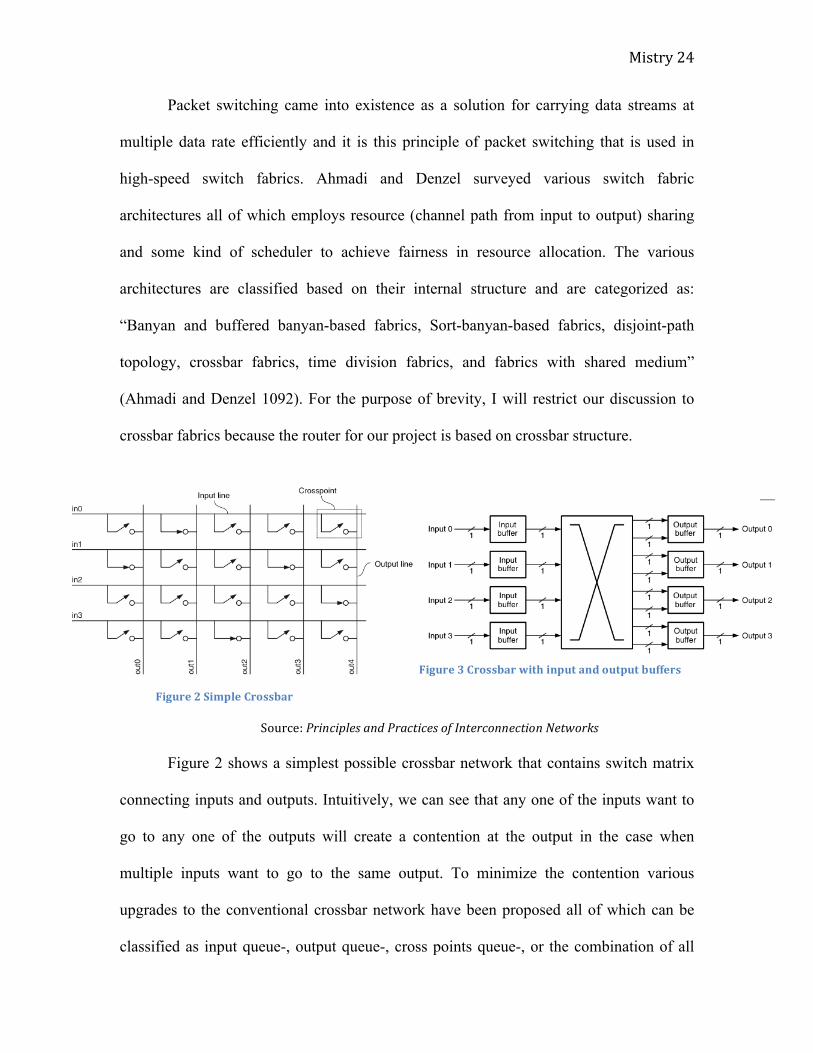
Source: Principles and Practices of Interconnection Networks
Packet switching came into existence as a solution for carrying data streams at
multiple data rate efficiently and it is this principle of packet switching that is used in
high-speed switch fabrics. Ahmadi and Denzel surveyed various switch fabric
architectures all of which employs resource (channel path from input to output) sharing
and some kind of scheduler to achieve fairness in resource allocation. The various
architectures are classified based on their internal structure and are categorized as:
“Banyan and buffered banyan-based fabrics, Sort-banyan-based fabrics, disjoint-path
topology, crossbar fabrics, time division fabrics, and fabrics with shared medium”
(Ahmadi and Denzel 1092). For the purpose of brevity, I will restrict our discussion to
crossbar fabrics because the router for our project is based on crossbar structure.
Figure 2 shows a simplest possible crossbar network that contains switch matrix
connecting inputs and outputs. Intuitively, we can see that any one of the inputs want to
go to any one of the outputs will create a contention at the output in the case when
multiple inputs want to go to the same output. To minimize the contention various
upgrades to the conventional crossbar network have been proposed all of which can be
classified as input queue-, output queue-, cross points queue-, or the combination of all
Figure 2 Simple Crossbar
Figure 3 Crossbar with input and output buffers
Mistry 25
depending upon the buffer location in the crossbar. A typical example of input and output
queue (buffer) crossbar is shown in figure 3. The idea is to buffer the data at either one of
these queues and schedule the buffered data to the output using various heuristics. The
scheduler that schedules the data through the crossbar is called arbiter that arbitrates the
data modestly such that maximum possible stored data reaches at their respective output
destination, although some of the buffered data may never reach to its output destination
in which case the agent again sends the data from the source. A detailed discussion about
the arbiters is covered by Yale Chen (2015). Mhamdi and Hamdi have discussed
crossbars achieving higher throughput using sophisticated scheduling algorithm and
improved structure.
Having talked about the evolution of switching networks and crossbars that is one
of the core components of the switching network, I’ll now discuss allocators – a
scheduling mechanism that allocates resources (data path from input to output) to the
incoming agents. The allocators discussed here will find its applications in building VC
allocators and switch allocators discussed in Technical Contribution section of Ian Juch
(2015) and Bhavana Chaurasia (2015) respectively. Selecting a proper allocation
mechanism is a design tradeoff for the routers in terms of latency and area (Ye Lu 358). It
means that a simple allocation technique may be cheap in term of the silicon area, but it is
less efficient in providing fairness to the resource allocation and thus increases the
latency for the input data to reach to the output destination. On the other hand, a more
complex allocation scheme can provide high throughput by allocating resources
efficiently thereby decreasing latency, but the silicon area of such complex allocation
scheme is larger.
Mistry 26
Allocators works on the principle of: “i) resources are only granted to agents that
requested them ii) each agent is granted access to at most one resource and iii) each
resource is granted to at most one agent” (Becker 28). To demonstrate the operation,
consider the following case:
Figure 4 shows a request, grant, and efficient grant matrix. Each row and column
represents an agent and a resource respectively. Thus, there are three agents and three
resources; agent 0 requested for resource 0,1, and 2; agent 1 requested resource 0 and 1;
agent 2 requested resource 0. Figure 4 (grant matrix) shows the resource allocation by an
inefficient allocator because it was only capable of allocating resource to agent 0 and 1
represented by dark dot. Agent 2 requested for resource 0 only that got allocated to agent
0 and thus according to principle (iii) resource 0 cannot be allocated to agent 2. Figure 4
(efficient grant matrix) shows a fair and efficient allocator that is capable of allocating
resources to all agents. Here none of the resources and agents is idle, thus demonstrating
an efficient allocation.
Different types of allocators are proposed based on the allocation mechanisms.
Becker and Dally discuss techniques that include separable allocation, wavefront
allocation, and maximum-size allocation. Separable allocators are of two types: separable
Figure 4 Request matrix, grant matrix, and efficient grant matrix
Mistry 27
input first in which first arbitration is done on incoming agents requesting resources and
then second round of arbitration is done on the resources to ensure each agent is granted
at the most only one resource; on the other hand, separable output first straight away
forward all the incoming requests to the associated resources and arbitration is done at the
output. Separable allocators are attractive for high-radix router because its delay (latency)
only increases logarithmically with the increase in port size, however they suffers the
disadvantage of weak fairness due to independent arbitration in the two rounds (Becker
31).
Poor fairness of separable allocation schemes can be overcome by implementing a
wavefront allocation scheme shown by Tamir and Chi. Wavefront allocator arbitrates
along the diagonal of the request-resource matrix (figure 3c) based on the priority cell
selection as opposed to linear arbitration employed by the separable allocators. The
grants generated along the diagonal of the request matrix are guaranteed to be singular
and thus maximum allocation is possible by iterating through the diagonals of the matrix.
Tamir and Chi (22) evaluated the performance of wavefront scheme in comparison with
other schemes and underscored its best performance with marginal complexity relative to
other schemes for high-radix routers.
METHODS AND MATERIALS This section will discuss methods employed and materials used during different
phase of the project. My project focus initiated with setting up of the VLSI tools after
which I executed a 32-radix (32-ports) router through various stages of the tools to
validate correct functioning of the tools and the router design. Next, I switched the focus
on to optimizing the runtime of the tools for large radix (64-radix) router. Lastly, I
redesigned the crossbar architecture to improve the runtime and area of the router. Tools
Mistry 28
setup for the router design began in the last week of October’14 and lasted throughout
December’14. Knowledge gained during the coursework of Introduction to Digital
Integrated Circuits (EE141) was used to setup the tool-flow. Tool includes CAD
software from Synopsys (EDA manufacturer) called Design Compiler (DC) and IC
Compiler (ICC). First step in the tool setup is to create a bashrc (UNIX file system) file
that contains the path to the tools location on the server. Next step is to create a separate
build directories for DC and ICC containing relevant scripts that executes necessary
commands needed to synthesize and place and route the router design (details of DC and
ICC commands are covered later in this section). Final step is to create a Makefile that is
a text file that links and executes various source files in order. The scripts containing DC
and ICC flow and their respective Makefiles were all built by BWRC research team, we
just used the existing infrastructure for our project.
After successful tools setup, I executed a 32-radix router design through the tool
flow. During the execution, DC complier synthesized a gate-level netlist of the Verilog
code. Gate-level netlist converts the Verilog behavioral code into a circuit netlist
containing logical gates. IC complier then generates a floorplan of the design and
performs the placement of the standard cells of the respective gates. It also performs the
routing of the standard cells with each other and with the synthesized clock tree. After
each step during the design execution, maintaining the correct functionality of the router
design is very important. Therefore, functional verification was carried out for Verilog
design, synthesized design, and placed and routed design using the provided test bench.
The Verilog design and synthesized design passed the functional check with the test
bench that was designed to provide “ideal” input stream of data. The input data is
Mistry 29
provided at the rising edge of the clock and it failed after placement and route (P&R)
stage because, the P&R design emulates close to real life circuit and thus the data
appearing at the input should take hold time into account. I diagnosed that since the input
data arrived right at the clock edge, P&R design encountered setup time violation and
resulted in functional error. After delaying the input data to account for the hold time, the
P&R design passes the functional check.
Figure 5 shows the “ideal” behavior of the test bench where the input data was
applied to the router right at the clock edge violating the setup time, while the violation
was corrected in figure 6 by providing the delay at the input of the router.
Figure 5 Input data at clock edge
Figure 6 Input data after clock edge
Mistry 30
After functional verification, my focus shifted towards optimizing the runtime of
the design execution through the tool flow. From hereon the term design execution in
context to the runtime optimization is equivalent to performing place and route on the
design. One of the two possible ways to go about optimization is to perform the
hierarchical execution of the design in which instead of executing entire design, the
hierarchical components of the design are executed incrementally to identify the specific
module of the design that takes maximum runtime (Yale Chen 2015). Another way for
1st round
2nd round
Figure 7 Conventional flow (left) and modified flow (right)
Mistry 31
the optimization, that I followed, is to strategically perform placement and routing such
that the tools execute simpler placement and routing before performing more arduous
optimization. In order to explain the runtime optimization, first I will show the default
placement and routing procedure and then show the modified version.
Figure 7 (left) shows the conventional tool flow. It starts with generating a
synthesized netlist using DC (compile_ultra command). Next, during the floorplan stage
IC complier creates a floor plan for the chip design where it indicates the location of
various standard cells in the design. It also specifies how close each standard cell is
placed relative to each other and thus provides an initial estimate for the area of the chip.
Further, floor planning includes deriving power and ground connection for the chip and it
also specifies the routing specific to each metal layer in the design. The floor plan along
with the synthesized netlist is fed to the IC complier for placement during which all the
standard cells are placed into the location specified during the floor plan stage. In
conventional flow, the placement and its optimization are done as a single step, which is
a time consuming process. After the placement, clock tree synthesis (CTS) is carried out.
CTS generates a buffer tree that takes the primary clock and distributes equally to all
parts of the design such that the fanout (load) is balanced in the entire design. Further
optimization is done after the placement and CTS to ensure the design meets the
specification provided in the floor plan. Finally, the clock tree and the standard cells are
routed and optimized for best possible timing and area requirements. In my opinion, the
two drawbacks in the conventional flow are independent generation of synthesized netlist
and the floor plan for the actual chip and the two iterations of the placement optimization
that is an expensive runtime process.
Mistry 32
The two drawbacks of the conventional flow are mitigated in the optimized flow
shown in figure 7 (right). Similar to the conventional flow, first the synthesized netlist is
generated from the Verilog code and is fed for the floor planning. The floor planning
information is then again fed to DC to re-synthesize the design conducive to the floor
planned design. The newly generated synthesized netlist is then fed to IC compiler for
placement during which first the initial placement is done unlike direct placement and
optimization in the conventional flow. The advantage of the initial placement is that it
reports the bottlenecks of the design in terms of congestion, power, timing, etc. Thus, the
following placement optimization can be targeted towards optimizing the bottleneck of
the design. Unlike the conventional flow, the clock tree synthesis in the optimized flow is
performed during the placement optimization stage thereby, eliminating additional
placement-optimization iteration performed in the conventional flow. Finally, the clock
routing and chip routing are performed similar to that in the conventional flow.
PS: The runtime optimization for the tools was referenced from the Design compiler and
IC compiler user manual from [12] and [13] respectively.
Mistry 33
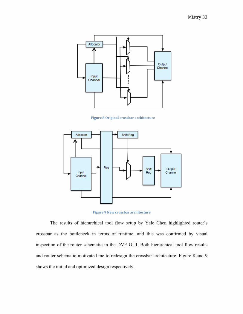
The results of hierarchical tool flow setup by Yale Chen highlighted router’s
crossbar as the bottleneck in terms of runtime, and this was confirmed by visual
inspection of the router schematic in the DVE GUI. Both hierarchical tool flow results
and router schematic motivated me to redesign the crossbar architecture. Figure 8 and 9
shows the initial and optimized design respectively.
Figure 8 Original crossbar architecture
Figure 9 New crossbar architecture
Mistry 34
Initial design consisted of number of multiplexers (mux) equal to the number of
ports, and each mux takes in input from all the input ports. This architecture can be
efficient for design that has input-output ports less than 32. Our targeted 64-ported design
blows up in area and runtime as the number of mux scaled with number of input-output
ports. The modified version uses a single mux that takes in input from all the input ports.
The select signals comes from a shift register that is clocked #ports times faster than the
original clock, for example, for 64-ports design the shift register needs to be clocked 65
times faster than the original clock to produce the select signals corresponding to each
input ports. The output of the mux is fed to another shift register that gets fed to the
output channel of the router. The resultant new crossbar architecture has pipelined the
overall router architecture. On the down side, producing fast clock that is #ports times
faster than the original clock can be impractical and therefore the practical solution is to
implement more multiplexers in the design that can reduce the ratio of fast clock and the
original clock. As an example, increasing the multiplexers from one to four will reduce
the ratio by factor of four, thus the new fast clock will have to be 16 times faster than the
original clock. Clearly, selecting number of multiplexers is a design tradeoff with
extremes at single multiplexer and number of multiplexers equal to the number of ports.
Results and Discussion section shows this tradeoff in plot of delay versus area.
RESULTS AND DISCUSSION In this section, I will discuss results pertaining to functional verification, design
space exploration, and runtime optimization. Functional verification provides the output
of the design for the given input vectors. The output varies with variations of the input
and thus it is important to perform functional verification with as many inputs
combination as possible. Provided test bench generates the stream of input packets of
Mistry 35
fixed length to be injected at each input ports. At the output, the flit sink collects the
output flits and accounts for number of input flits versus number of output flits.
Functional verification for various port sizes were measured and for each router
configuration, flit size was fixed at 64bits and each input channel consisted of 128 bytes
buffer. The result is tabulated in Table 1.
Table 1 shows total number of flits sent to the router and number of flits that came
out of the router for different port sizes. Port sizes 5 and 16 were successfully able to
produce all the flits at the output while, for port sizes 32 and 64 number of flits going into
the router were decreased. Moreover, for 32 and 64 ports router not all incoming flits
comes out of the router successfully. This can be attributed to the fact that as the port size
increases the efficiency of arbiter for resource allocation decreases and part of the flits are
lost within the router itself.
Number of Ports
in Router
Incoming
Flits
Outgoing Flits
5 13260 13260
16 20234 20234
32 11995 6226
64 5210 3790
Table 1 Functional verification results
Mistry 36
Area (mm2) Power Critical Path
(nS) Total (W) Leakage (W)
5-radix 0.18 0.022 0.016 3.51
32-radix 2.25 0.34 0.284 8.85
64-radix 11.65 1.27 1.15 11.81
Table 2 Area, power, and timing for routers
Area (mm2) Power
Critical Path (nS) Total (W) Leakage (W)
128-radix 40 7.35 6.75 NA
256-radix 160 36.75 33.75 NA
Table 3 Extrapolated area, power, and timing
Table 2 reports the area, power, and timing of 5-, 32-, and 64-radix routers after the place
and route stage. As the size of the router is doubled its area increases by a factor of ~4.
Similarly, the power number grows by the factor of ~5, while the critical path length has
no consistent pattern. Original goal of the project was to design a high radix for example
128-radix or 256-radix router, so if we extrapolate the preliminary results from above
table for 128- and 256- radix router then the resultant design will look something like the
one shown in Table 3. Due to run time limitations, we were unable to scale the router
beyond 64 ports and all the subsequent results are based on 64-port router.
The run time optimization by changing the tool flow resulted in runtime gain of
~3 hours for 32-port router i.e. runtime reduced from original ~8-10 hours to less than 6
hours. However, the gain for 64-port router was insignificant in terms of total run time.
Mistry 37
The new run time with modified tool flow is ~30 hours down from original ~36 hours.
Despite the gain, the modified tool flow didn’t help much.
As expected, the greatest advantage in terms of reducing the total run time of the
tools and area minimization was achieved by redesigning the crossbar architecture. The
total run time for 64-port router with number of multiplexers equal to 1, 4, and 8 is less
than 15 hours, while for number of multiplexers equal to 32 the run time is ~20 hours.
Each of these configurations has clear run time advantage than the original 64
multiplexers design with the run time of more than 36 hours. However, this advantage
came at the cost of adding extra clock (fast clock) to the router crossbar. For the 64-port
design the magnitude of the fast clock is dependent on the number of multiplexers
implemented in the crossbar architecture, with the smallest number of multiplexer equal
to one that required fast clock to be 65 times faster than the original clock. And for
number of multiplexers equal to the number of input-output ports, fast clock is equal to
the slow clock. Table 4 shows the area, power, and critical path for 64-port router with
different number of multiplexers.
Multiplexer Area (mm2)
Critical Path (nSec)
Power
Leakage (Watts)
Total power (Watts)
1 6.03 10.03 0.486 0.597
4 6.22 10.03 0.506 0.617
8 6.44 10.02 0.522 0.634
32 7.96 10.16 0.659 0.778
64 11.65 11.81 1.15 1.27
Table 4 Area, critical path, and power with new crossbar
Mistry 38
Figure 10 and 11 shows the plots of area versus delay and total power versus
delay for a 64-port router with different number of multiplexers at 10% core utilization.
Based on both the plots, an optimum 64-port router has the delay between 50 to 90nSec
with area ~6.5mm2 and total power of ~0.65 Watts.
Mistry 39
Figure 10 Area versus delay for different number of multiplexers
Figure 11 Power versus delay for different number of multiplexers
Mistry 40
Conclusion In conclusion we studied and analyzed a network-on-chip router from various
sources. Following that, we implemented a high-radix router based on Becker’s Verilog
implementation of the router. The run time of the VLSI tools appeared to be primary
bottleneck in scaling the router beyond 64-ports and so we carried out various
optimizations in the tool flow including hierarchical implementation of the tool flow
(Yale Chen 2015), setting optimization flags (Ian Juch 2015), and modifying the tool
scripts. Finally, the modified crossbar architecture reduced the run time from originally
36+ hours down to ~15 hours. It also reduced the area of the router down from ~11 mm2
to ~6-7 mm2. Current outcomes in the router achieves the bandwidth of ~0.4 terabyte,
which is 10,000 times less in magnitude than original goal of peta-bit.
Further improvements in the current router implementation can be achieved by
moving the pipeline register between the allocator. Allocator functions by arbitrating on
the input side first followed by output arbitration. Placing pipelined register between
input and output arbitration will reduce the critical path that is along the feedback path
from allocators to the input channel and will result in further increase in the speed of the
router. However, placing a pipeline register along a feedback path in combinational loop
is challenging in general and requires sophisticated architectural implementation like loop
unrolling. I have finished implementing the pipeline register along the feed back path and
currently in the process of debugging bugs associated with the break up of the feed back
loop.
Like many industry-based projects, the success of our project is also attributed to
the efficient project management implemented by all the team members besides other
factors. Strict adherence to weekly advisor’s and team meeting allowed us to adapt
Mistry 41
different dynamics during the course of the project. Periodic documentation of the results
based on weekly task helped us to constantly analyze the scope of the project and helped
us maneuver from undesirable path. As an example, we realize early on in the spring
semester that due to limitations in the run time of the tools, we should not scale the router
beyond 64 ports without diagnosing and troubleshooting the limitations. This prevented
us from spending resources and time on large ports router and rather kept our focus
maintained in improving the 64-port router. Lastly, excellent offline communication
between the team members catalyzed the task actions for each team members.
Finally, we plan to upload all the project work including tool flow setup (Ian Juch
2015), SRAM integration (Ian Juch and Surabhi Kumar 2015), hierarchical
implementation of the tool flow (Yale Chen 2015), critical path analysis and different
arbiter’s implementation (Bhavana Chaurasia 2015), modified scripts in the tool flow and
redesigned crossbar architecture (Mistry Jay 2015) onto the GIT repo that can be readily
utilized by future team.
Mistry 42
Bibliography [1] Becker, Daniel U., “Efficient Microarchitecture for Network-on-Chip Routers,” Phd
thesis. Stanford. August 2012 [2] Dally, William J., and Brian Towles. Principles and Practices of Interconnection
Networks. Amsterdam: Morgan Kaufmann, 2004. Print. [3] Ahmadi, H.; Denzel, W.E., "A survey of modern high-performance switching
techniques," Selected Areas in Communications, IEEE Journal on , vol.7, no.7, pp.1091,1103, Sep 1989 doi: 10.1109/49.44557
[4] Juch, Ian., “Technical Contributions to Petabit Switch Fabric Design,” Capstone Project Report. University of California, Berkeley. March 2015.
[5] Chaurasia, Bhavana., “Technical Contributions to Petabit Switch Fabric Design,” Capstone Project Report. University of California, Berkeley. March 2015.
[6] Chen, Yale., “Technical Contributions to Petabit Switch Fabric Design,” Capstone Project Report. University of California, Berkeley. March 2015.
[7] Kumar, Surabhi., “Technical Contributions to Petabit Switch Fabric Design,” Capstone Project Report. University of California, Berkeley. March 2015.
[8] Mhamdi, L.; Hamdi, M., "CBF: a high-performance scheduling algorithm for buffered crossbar switches," High Performance Switching and Routing, 2003, HPSR. Workshop on, vol., no., pp.67,72, 24-27 June 2003 doi: 10.1109/HPSR.2003.1226682
[9] Yoshigoe, K.; Christensen, K.J., "An evolution to crossbar switches with virtual output queuing and buffered cross points," Network, IEEE, vol.17, no.5, pp.48,56, Sept.-Oct. 2003 doi: 10.1109/MNET.2003.1233917
[10] Ye Lu; Changlin Chen; McCanny, J.; Sezer, S., "Design of interlock-free combined allocators for Networks-on-Chip," SOC Conference (SOCC), 2012 IEEE International, vol., no., pp.358,363, 12-14 Sept. 2012 doi: 10.1109/SOCC.2012.6398332
[11] Becker, D.U.; Dally, W.J., "Allocator implementations for network-on-chip routers," High Performance Computing Networking, Storage and Analysis, Proceedings of the Conference on , vol., no., pp.1,12, 14-20 Nov. 2009 doi: 10.1145/1654059.1654112
[12] Tamir, Y.; Chi, H.-C., "Symmetric crossbar arbiters for VLSI communication switches," Parallel and Distributed Systems, IEEE Transactions on , vol.4, no.1, pp.13,27, Jan 1993 doi: 10.1109/71.205650
[13] Design Compiler User Guide. Version F-2011.09, Sept. 2011. Design Compiler. Synopsys, Mountain View, CA.
[14] IC Compiler Implementation User Guide. Version F-2011.09, Sept. 2011. IC Compiler. Synopsys, Mountain View, CA.
[15] Clark, Don. “Startup has big plans for tiny chip technology”. Wall Street Journal. 3 May 2011. Accessed 5 April 2015.
[17] Boyland, Kevin. 2013 IBISWorld Industry Report OD4540: Electronic Design Automation Software Developers in the US. http://www.ibis.com, accessed February 13, 2015.
[18] Broadcom. Broadcom Delivers Industry's First High-Density 25/100 Gigabit Ethernet Switch for Cloud-Scale Networks. Press Release. N.p., 24 Sept. 2014. Web. 1 Mar. 2015. <http://www.broadcom.com/press/release.php?id=s872349>.
[19] “Computing: Battle of the Clouds”. The Economist. 15 October 2009. http://www.economist.com/node/14644393?zid=291&ah=906e69ad01d2ee51960100b7f502595.
[20] Deangelis, Stephen F. “Closing in on Quantum Computing”. Wired. 16 October 2014. http://www.wired.com/2014/10/quantum-computing-close/
[21] Handy, Jim. 2014 Semiconductors A Crazy Industry. http://www.forbes.com/sites/jimhandy/2014/02/11/semiconductorsacrazyindustry2/, accessed February 16, 2015.
[22] Hoover’s. “Semiconductor and other electronic component manufacturing: Sales Quick Report”. http://subscriber.hoovers.com/H/industry360/printReport.html?industryId=1859 &reportType=sales, accessed February 11, 2015.
[23] Hulkower Billy, “ Consumer Cloud Computing- Issues in the market”, Mintel (2012).
[24] Kahn, Sarah. 2014 IBISWorld Industry Report 33421: Telecommunication Networking Equipment Manufacturing in the US. http://www.ibis.com, accessed February 10, 2015.
[25] Kahn, Sarah. 2014 IBISWorld Industry Report 51721: Wireless Telecommunications Carriers in the US. http://www.ibis.com, accessed February 26, 2015.
[26] Porter, Michael. “The Five Competitive Forces That Shape Strategy”. Harvard Business Review. January 2008.
[27] “The Server Market: Shifting Sands”. The Economist. 1 June 2013. http://www.economist.com/news/business/21578678-upheaval-less-visible-end-computer-industry-shifting-sands.
[28] Ulama, Darryle. 2014 IBISWorld Industry Report 33441a: Semiconductor & Circuit Manufacturing in the US. http://www.ibis.com, accessed February 10, 2015.
[29] Ulama, Darryle. 2014 IBISWorld Industry Report 33329a: Semiconductor Machinery Manufacturing in the US. http://www.ibis.com, accessed February 10, 2015.
[30] Ulama, Darryle. 2014 IBISWorld Industry Report 33411a: Computer Manufacturing
Mistry 44
in the US. http://www.ibis.com, accessed February 10, 2015.