Photonics Design Automation and MPW Runs for Affordable Chip Production design tools, design kits and collaboration PIC TRAINING NYC 2015 COLUMBIA UNIVERSITY, NEW YORK, USA, OCTOBER 19-23 2015 TWAN KORTHORST
Transcript
Photonics Design Automation and MPW Runs for Affordable Chip Production
design tools, design kits and collaboration
PIC TRAINING NYC 2015C O LU M B I A U N I V E R S I T Y, N E W YO R K , U S A , O C TO B E R 1 9 - 2 3 2 0 1 5
TWAN KORTHORST
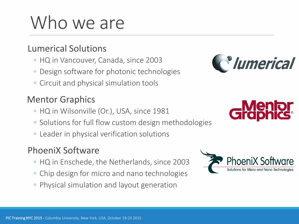
Lumerical Solutions◦ HQ in Vancouver, Canada, since 2003
◦ Design software for photonic technologies
◦ Circuit and physical simulation tools
Mentor Graphics◦ HQ in Wilsonville (Or.), USA, since 1981
◦ Solutions for full flow custom design methodologies
◦ Leader in physical verification solutions
PhoeniX Software◦ HQ in Enschede, the Netherlands, since 2003
◦ Chip design for micro and nano technologies
◦ Physical simulation and layout generation
Who we are
PIC Training NYC 2015 - Columbia University, New York, USA, October 19-23 2015
Electronics market is mature◦ Total electronic components markets is > 500B$, with IC’s ~250B$
◦ Electronics Design Automation (EDA) market just under 10B$
Mature (silicon) electronics industry comes with◦ Fabless business model dominant
◦ Good array of foundries (TSMC, GF, Jazz, IBM, etc.)
◦ Well developed EDA industry (Synopsys, Cadence, Mentor Graphics)
Existing technologies are reaching bandwidth limitations◦ Power consumption (heat) dominated by data transfer rather than
computing
◦ Density
3
Why integrated photonics?
PIC Training NYC 2015 - Columbia University, New York, USA, October 19-23 2015
• Market need drives transition to integrated photonics solutions• Datacenters and High Performance Computing
• Number of components: 10’s – 1000’s per chip (relates to 10k – 1M primitives)
• RF-like or analog behavior (Telecom C-band is 1530 – 1565 nm ~ 193 THz)
• Design closely related with fabrication
• Process and temperature dependencies
6
With some key differences
Sou
rce:
Kai
am
PIC Training NYC 2015 - Columbia University, New York, USA, October 19-23 2015
• Fabrication: thin film technologies, lithography
• Design flow: verified mask layout design as final step
• Photonics is where electronics was in the 80’s• Transition from PCB to (silicon) IC
• Large number of (small) fabs providing manufacturing capacity
• Many software suppliers, each covering parts of the design flow
• Emerging standardization in processes and tools
7
There are many similarities between electronics and photonics
Sou
rce:
IBM
PIC Training NYC 2015 - Columbia University, New York, USA, October 19-23 2015
• You need an application specific PIC
Please note that electronic ICs have paved the road for 50 years
• You need to decide on material and foundry• Options: InP, Silicon, or TriPleX (excluding PLC and LiNbO3)
• Also need to decide on MPW vs. a custom run• MPW reduces costs, but custom runs might be needed in the end
(for volume and/or for unique performance)
8
If you need a PIC, where do you go?
PIC Training NYC 2015 - Columbia University, New York, USA, October 19-23 2015
9
Decide on material
PIC Training NYC 2015 - Columbia University, New York, USA, October 19-23 2015
Multi Project Wafer runs versus Custom runs
• MPW users all share the same generic fabrication process• Cost sharing: multiple designs at same mask/wafer
• Imposes limits, but comes with a library of building blocks
• “Lego” building blocks allow for virtually all PICs
• >500 PICs developed in generic fabs via MPW runs
• There are several key players, mainly in Europe:• Silicon photonics: CEA-Leti, IHP, IME, IMEC, VTT
• InP: FhG/HHI, Oclaro, SMART Photonics
• TriPleX (SiN): LioniX
• AIM Photonics won the IP-IMI award in the US
• And … don’t forget about packaging
10
Decide on foundry
PIC Training NYC 2015 - Columbia University, New York, USA, October 19-23 2015
11
Decide on foundry
PIC Training NYC 2015 - Columbia University, New York, USA, October 19-23 2015
12
Typical timelines
PIC Training NYC 2015 - Columbia University, New York, USA, October 19-23 2015
13
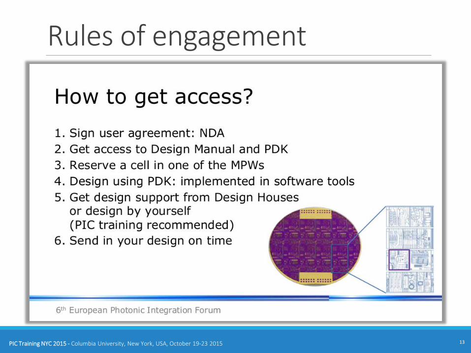
Rules of engagement
PIC Training NYC 2015 - Columbia University, New York, USA, October 19-23 2015
• Fabrication: thin film technologies, lithography
• Design flow: verified mask layout design as final step
• Photonics is where electronics was in the 80’s• Transition from PCB to (silicon) IC
• Large number of (small) fabs providing manufacturing capacity
• Many software suppliers, each covering parts of the design flow
• Emerging standardization in processes and tools
14
There are many similarities between electronics and photonics
Sou
rce:
IBM
PIC Training NYC 2015 - Columbia University, New York, USA, October 19-23 2015
• Today really good design solutions are available• Electronics Design Automation (EDA) made for Electronic ICs
• Likewise, Photonic Design Automation (PDA) being created for PICs
• But there are in between situations:• What if your chip has optical as well as electrical components?
• What if you plan to do the photonic simulations in PDA, but then use EDA for the mask layout?
• And, there are ongoing efforts between EDA and PDA providers to make their S/W interoperable and support the industry to scale from R&D to (volume) manufacturing
• Even though some functions can be done using both PDA as well as EDA, some care is needed…
15
PIC Design Software
PIC Training NYC 2015 - Columbia University, New York, USA, October 19-23 2015
16
EDA and PDA: photonics ≠ CMOS
17
EDA and PDA: photonics ≠ CMOS
Analog design time syndrome“for a 10% analog 90% digital IC, the analog design takes 90% of the design time”
PIC Training NYC 2015 - Columbia University, New York, USA, October 19-23 2015
Requires for simulations:◦ Dedicated photonic circuit simulation tools
◦ Special physical simulation tools for integrated photonics
◦ Interaction between electronics and photonics
Requires for mask layout:◦ Accurate and flexible definition of all angle shapes
◦ Advanced gridding and fracturing of polygons
◦ P-cell like definition for primitives and compounds
◦ Special features for verification (DRC, LVS)
18
Integrated Photonics Design
PIC Training NYC 2015 - Columbia University, New York, USA, October 19-23 2015
19
Tools available for full flow
PIC Training NYC 2015 - Columbia University, New York, USA, October 19-23 2015
• Pick, place and connect validated components
• Photonic and electrical connections automatically detected
• Schematic connectivity will drive layout directly
p20
Tools support circuit design
PIC Training NYC 2015 - Columbia University, New York, USA, October 19-23 2015
• Calibrated model libraries improve design accuracy
• Design using compact model libraries of fundamental and complex devices, calibrated to foundry processes
• Frequency & time domain simulation
p21
Tools support circuit simulations
PIC Training NYC 2015 - Columbia University, New York, USA, October 19-23 2015
22
Tools support component design
Spiral delay-line, defined by either geometrical or optical parameters
Wide variety of layout primitives available to design custom components, like a parametrized sine-bend
PIC Training NYC 2015 - Columbia University, New York, USA, October 19-23 2015
• Propagation simulations: eg. FDTD, EME, BPM
• Mode simulations: eg. mode-solvers, CMT
23
Tools support component simulations
PIC Training NYC 2015 - Columbia University, New York, USA, October 19-23 2015
Pick, place and route or schematic driven layout
p24
Tools support circuit mask layout
PIC Training NYC 2015 - Columbia University, New York, USA, October 19-23 2015
Design software can translate design intent into layout
… and correct for process influences
p25
Tools support mask layout
Simulating lithographyinfluence on design intent
Use technology information to obtain design intent after
fabrication
Xu Wang, et al., "Lithography Simulation for the Fabrication of Silicon Photonic Devices with Deep-Ultraviolet Lithography", IEEE GFP, 2012
PIC Training NYC 2015 - Columbia University, New York, USA, October 19-23 2015
Functional verification, Design Rule Checking (DRC) and Layout vs Schematic (LVS)
Built-in photonics relevant design checks(like minimum bend radius)
Design rules targeting CMOS processes will flag thousands of false errors in photonic structures, Photonic specific DRC rules can minimize false errors
Integrated design flows enable LVS
p26
Tools support verification
PIC Training NYC 2015 - Columbia University, New York, USA, October 19-23 2015
27
Why are PDKs so important?
PIC Training NYC 2015 - Columbia University, New York, USA, October 19-23 2015
28
Why are PDKs so important?
PIC Training NYC 2015 - Columbia University, New York, USA, October 19-23 2015
When working with a foundry (or your own fab), you do not want to reinvent the wheel nor make unnecessary mistakes
So all relevant knowledge should be available when designing a PIC
And the PDK should be automated (rather than in the form of docs)
Without a PDK, there are simply too many unneeded iterations
What does a PDK include?
Design rules and mask layer information
Library of validated components
Layout information
Simulation models and settings
Die and package templates
Why are PDKs so important?
29PIC Training NYC 2015 - Columbia University, New York, USA, October 19-23 2015
Faster design cycles and first-time-right designs
Higher accuracy by using validated compact model libraries for circuit design
Faster layout implementation by using predefined parametric components
Higher yield in manufacturing by applying design rules
p30
Photonic Circuit Design & Fabrication
System Designer
Component & Model Library Design
Component Designer
Photonic PDKDesign Rules Component parametersProcess data
PIC Training NYC 2015 - Columbia University, New York, USA, October 19-23 2015
User / Designer
Three Distinct Design Activities for PIC Development
1. Component-level design and optimization◦ Design and optimize a component for desired performance
2. Compact model library generation for PDKs◦ Build compact model for component
◦ Calibrate against experimental results
◦ Inform with simulation results
3. Photonic Integrated Circuit design and optimization◦ Build complex circuits based on known
components with validated compact models
Why Lumerical?
p40
User / Designer
Access Partners
Fabrication Packaging
User / Designer
Access Partners
Fabrication Packaging
PIC Training NYC 2015 - Columbia University, New York, USA, October 19-23 2015
Why Lumerical?
p41
PDKsDesign Rules,
Compact Models
Component Parameters
Process Data
Photonic Component DesignOptoelectronic Solvers,
Experimental Data
Compact Model Parameter Extraction
FDTD SolutionsNanophotonic Solver
(2D/3D)
MODE SolutionsWaveguide Design
Environment
DEVICECharge Transport
Solver (2D/3D)
INTERCONNECTPhotonic Integrated Circuit
Simulator
Layout InformationProcess InformationDesign Rules
• Parameter Extraction for Compact Models
• Component Design & Optimization
Compact Model Library for Circuit Design &
Optimization
PIC Training NYC 2015 - Columbia University, New York, USA, October 19-23 2015
• Focus on Design for Manufacturability
• We have been supporting 100’s of designers (MPW-users and at
vertically integrated organizations) getting started with PIC design
• More than 25 years photonics design and tools expertise, available trough excellent customer support• Our support is valued by our customers with a 9.1 out of 10
p42
Why PhoeniX Software?
PIC Training NYC 2015 - Columbia University, New York, USA, October 19-23 2015
• Native all-angle and all-shape design
• Complete parametrized library for photonics
• Includes photonics verification and design rule checking
• Interfaces with world-class 3rd party circuit simulators
• Enables EDA centric design flows
• Easy to use GUI including powerful scripting
• PDKs available for 8 photonics foundry services
More than 300 designs created and fabricated in MPW’s in the last 3 years!
p43
Why OptoDesigner?
PIC Training NYC 2015 - Columbia University, New York, USA, October 19-23 2015
Further Informationwww.lumerical.com
More material including demo movies for the EDA-style design flow: www.lumerical.com/tcad-products/interconnect/pyxis_eda/
And for the INTERCONNECT – OptoDesigner interface: www.lumerical.com/phoenix/
www.mentor.com
A generic, non-proprietary silicon photonics design kit is available for download at www.siepic.ubc.ca/GSiP
www.phoenixbv.com/optodesigner
Overview of available PDKs: www.phoenixbv.com/designkits
44PIC Training NYC 2015 - Columbia University, New York, USA, October 19-23 2015