53
A product of a PHYTEC Technology Holding company phyCORE-TriCore Development Board Hardware Manual Edition march 2009

A product of a PHYTEC Technology Holding company
phyCORE-TriCore Development Board
Hardware Manual
Edition march 2009

phyCORE-TriCore Development Board
© PHYTEC Messtechnik GmbH 2009 L-730e_0
In this manual are descriptions for copyrighted products that are not explicitly indicated as such. The absence of the trademark (™) and copyright (©) symbols does not imply that a product is not protected. Additionally, registered patents and trademarks are similarly not expressly indicated in this manual. The information in this document has been carefully checked and is believed to be entirely reliable. However, PHYTEC Messtechnik GmbH assumes no responsibi-lity for any inaccuracies. PHYTEC Messtechnik GmbH neither gives any guar-antee nor accepts any liability whatsoever for consequential damages resulting from the use of this manual or its associated product. PHYTEC Messtechnik GmbH reserves the right to alter the information contained herein without prior notification and accepts no responsibility for any damages which might result. Additionally, PHYTEC Messtechnik GmbH offers no guarantee nor accepts any liability for damages arising from the improper usage or improper installation of the hardware or software. PHYTEC Messtechnik GmbH further reserves the right to alter the layout and/or design of the hardware without prior notification and accepts no liability for doing so. © Copyright 2009 PHYTEC Messtechnik GmbH, D-55129 Mainz. Rights - including those of translation, reprint, broadcast, photomechanical or similar reproduction and storage or processing in computer systems, in whole or in part - are reserved. No reproduction may occur without the express written consent from PHYTEC Messtechnik GmbH. EUROPE NORTH AMERICA
Address: PHYTEC Technologie Holding AGRobert-Koch-Str. 39 D-55129 Mainz GERMANY
PHYTEC America LLC 203 Parfitt Way SW, Suite G100 Bainbridge Island, WA 98110 USA
Ordering Information:
+49 (800) 0749832 [email protected]
1 (800) 278-9913 [email protected]
Technical Support:
+49 (6131) 9221-31 [email protected]
1 (800) 278-9913 [email protected]
Fax: +49 (6131) 9221-33 1 (206) 780-9135
Web Site: http://www.phytec.de http://www.phytec.com preliminary Edition: Mar 2009

Table of Contents
© PHYTEC Meßtechnik GmbH 2009 L-730e_0
Preface 1 1 The phyCORE-TriCORE Development Board ............................... 3
1.1 Concept of the phyCORE Development Board ........................... 3 1.2 phyCORE-TriCORE Development Board Connectors and
Jumpers......................................................................................... 5 1.2.1 Connectors....................................................................... 5 1.2.2 Jumpers on the phyCORE-TriCORE Development
Board ............................................................................... 7 1.3 Functional Components on the phyCORE-TriCORE
Development Board.................................................................... 10 1.3.1 Power Supply at X1 ...................................................... 10 1.3.2 Activating the Bootstrap Loader ................................... 11 1.3.3 First Serial Interface at Socket P1A.............................. 14 1.3.4 Second Serial Interface at Socket P1B.......................... 15 1.3.5 First CAN Interface at Plug P2A .................................. 16 1.3.6 Second CAN Interface at Plug P2B .............................. 19 1.3.7 RJ45 Ethernet Connector X7 ........................................ 22 1.3.8 Programmable LED D3 ................................................ 22 1.3.9 Pin Assignment Summary of the phyCORE, the
Expansion Bus and the Patch Field............................... 23 1.3.10 DS2401 Silicon Serial Number..................................... 36 1.3.11 Pin Header Connectors X10.......................................... 37 1.3.12 USB Wiggler connector X11 ....................................... 37 1.3.13 LCD connector .............................................................. 38 1.3.14 JTAG PLD connector only for phyCORE-TC1130 ..... 40 1.3.15 USB connector X12 ...................................................... 41 1.3.16 OCDS2 connector only for phyCORE-TC1796 ........... 42
2 Revision History ................................................................................ 43 Appendice A ............................................................................................... 44
A.1 Release Notes ............................................................................. 44 Index .................................................................................................... 45

phyCORE-TriCore Development Board
© PHYTEC Messtechnik GmbH 2009 L-730e_0
Index of Figures Figure 1: Modular Development and Expansion Board Concept with the
phyCORE-TC1130 or phyCORE-TC1796................................ 4
Figure 2: Location of Connectors on the phyCORE-TriCORE Development Board ................................................................... 6
Figure 3: Numbering of Jumper Pads ....................................................... 7
Figure 4: Location of the Jumpers (View of the Component Side) .......... 7
Figure 5: Default Jumper Settings of the phyCORE-TriCORE Development Board for Standard phyCORE-TC1130.............. 8
Figure 6: Default Jumper Settings of the phyCORE-TriCORE Development Board for Standard phyCORE-TC1796............. 9
Figure 7: Connecting the Supply Voltage at X1 ..................................... 10
Figure 8: Pin Assignment of the DB-9 Socket P1A as First RS-232 (Front View) ............................................................................ 14
Figure 9: Pin Assignment of the DB-9 Socket P1A as Second RS-232 (Front View) ............................................................................ 15
Figure 10: Pin Assignment of the DB-9 Plug P2A (CAN Transceiver on phyCORE-TC1130, Front View) ............................................ 16
Figure 11: Pin Assignment of the DB-9 Plug P2A (CAN Transceiver on Development Board)................................................................ 17
Figure 12: Pin Assignment of the DB-9 Plug P2A (CAN Transceiver on Development Board with Galvanic Separation) ...................... 18
Figure 13: Pin Assignment of the DB-9 Plug P2B (CAN Transceiver on phyCORE-TC1130, Front View) ............................................ 19
Figure 14: Pin Assignment of the DB-9 Plug P2B (CAN Transceiver on Development Board)................................................................ 20
Figure 15: Pin Assignment of the DB-9 Plug P2B (CAN Transceiver on Development Board with Galvanic Separation) ...................... 21
Figure 16: Pin Assignment Scheme of the Expansion Bus....................... 24
Figure 17: Pin Assignment Scheme of the Patch Field............................. 24
Figure 18: Connection of the DS2401 Silicon Serial Number................. 36

Table of Contents
© PHYTEC Meßtechnik GmbH 2009 L-730e_0
Index of Tables Table 1: JP12 Configuration of the Boot Button .................................. 11
Table 2: JP20, JP21, JP13 Configuration of Boot via RS-232 ............. 12
Table 3: Jumper Configuration for the First RS-232 Interface .............. 14
Table 4: Jumper Configuration for the Second RS-232 Interface ......... 15
Table 5: Jumper Configuration for CAN Plug P2A Using the CAN Transceiver on the phyCORE-TC1130 or phyCORE-TC179616
Table 6: Jumper Configuration for CAN Plug P2A Using the CAN Transceiver on the Development Board .................................. 17
Table 7: Jumper Configuration for CAN Plug P2A Using the CAN Transceiver on the Development Board with Galvanic Separation................................................................................. 18
Table 8: Jumper Configuration for CAN Plug P2B Using the CAN Transceiver on the phyCORE-TC1130 or phyCORE-TC179619
Table 9: Jumper Configuration for CAN Plug P2B Using the CAN Transceiver on the Development Board .................................. 20
Table 10: Jumper Configuration for CAN Plug P2B Using the CAN Transceiver on the Development Board with Galvanic Separation................................................................................. 21
Table 11: JP2-6 ,JP10,JP11, Configuration of the Ethernet Interface ..... 22
Table 12: JP18 Configuration of the Programmable LED D3................ 22
Table 13: Pin Assignment for the phyCORE-TC1130, phyCORE-TC1796 and Development Board / Expansion Board ............. 26
Table 14: Pin Assignment for the phyCORE-TC1130, phyCORE-TC1796 and Development Board / Expansion Board ............. 29
Table 15: Pin Assignment for the phyCORE-TC1130, phyCORE-TC1796 and Development Board / Expansion Board ............. 31
Table 16: Pin Assignment for the phyCORE-TC1130, phyCORE-TC1796 and Development Board / Expansion Board ............. 33
Table 17: Pin Assignment for the phyCORE-TC1130, phyCORE-TC1796 and Development Board / Expansion Board ............. 33

phyCORE-TriCore Development Board
© PHYTEC Messtechnik GmbH 2009 L-730e_0
Table 18: Pin Assignment for the phyCORE-TC1130, phyCORE-TC1796 and Development Board / Expansion Board ............. 34
Table 19: Pin Assignment Power Supply for the phyCORE-TC1130 / Development Board / Expansion Board .................................. 34
Table 20: Pin Assignment for the phyCORE-TC1130, phyCORE-TC1796 and Development Board / Expansion Board ............. 35
Table 21: JP1 Jumper Configuration for Silicon Serial Number Chip .... 36
Table 22: Jumper Configuration for T6963C LCD-Controller ............... 38
Table 23: Jumper Configuration for HD61202, HD44780...................... 39
Table 24: contrast Configuration LCD .................................................... 39
Table 25: Pin assignemt JTAG_PLD connector for ................................ 40
Table 26: Jumper Configuration for X12 USB connector for phyCORE-TC1130 .................................................................................... 41
Table 27: Jumper Configuration for X12 USB connector for phyCORE-TC1796 .................................................................................... 41

Preface
Preface
This Hardware Manual describes only the functions of PHYTEC phyCORE-TriCORE Development Board for the phyCORE-TC1130 and phyCORE-TC1796 module. The controllers and modules are not described herein. Precise specifications for Infineon’s TC1130 or TC1796 Tricore microcontroller series controller can be found in the enclosed microcontroller Data Sheet/User's Manual. If software is included please also refer to additional documentation for this software. In this hardware manual and in the attached schematics, low active signals are denoted by a "/" in front of the signal name (i.e.: /RD). A "0" indicates a logic-zero or low-level signal, while a "1" represents a logic-one or high-level signal. Declaration of Electro Magnetic Conformance of the PHYTEC phyCORE-TriCORE Development Board PHYTEC Single Board Computers (henceforth products) are designed for installation in electrical appliances or as dedicated Evaluation Boards (i.e.: for use as a test and prototype platform for hardware/software development) in laboratory environments. Caution: PHYTEC products lacking protective enclosures are subject to damage by ESD and, hence, may only be unpacked, handled or operated in environments in which sufficient precautionary measures have been taken in respect to ESD-dangers. It is also necessary that only appropriately trained personnel (such as electricians, technicians and engineers) handle and/or operate these products. Moreover, PHYTEC products should not be operated without protection circuitry if connections to the product's pin header rows are longer than 3 m.
© PHYTEC Meßtechnik GmbH 2009 L-730e_0 1

phyCORE-TriCore Development Board
2 © PHYTEC Meßtechnik GmbH 2009 L-730e_0
PHYTEC products fulfill the norms of the European Union’s Directive for Electro Magnetic Conformance only in accordance to the descriptions and rules of usage indicated in this hardware manual (particularly in respect to the pin header row connectors, power connector and serial interface to a host-PC). Implementation of PHYTEC products into target devices, as well as user modifications and extensions of PHYTEC products, is subject to renewed establishment of conformity to, and certification of, Electro Magnetic Directives. Users should ensure conformance following any modifications to the products as well as implementation of the products into target systems.
This Development Board supports the phyCORE-TC1130 and the phyCORE-TC1796. PHYTEC supports all common 8- and 16-bit as well as selected 32-bit controllers in two ways: (1) as the basis for Rapid Development Kits which serve as a
reference and evaluation platform (2) as insert-ready, fully functional micro-, mini- and phyCORE
OEM modules, which can be embedded directly into the user’s peripheral hardware, design.
PHYTEC's microcontroller modules allow engineers to shorten development horizons, reduce design costs and speed project concepts from design to market.

phyCORE-TriCore Development Board
© PHYTEC Meßtechnik GmbH 2009 L-730e_0 3
1 The phyCORE-TriCORE Development Board
PHYTEC Development Boards are fully equipped with all mechanical and electrical components necessary for the speedy and secure start-up and subsequent communication to and programming of applicable PHYTEC Single Board Computer (SBC) modules. Development Boards are designed for evaluation, testing and prototyping of PHYTEC Single Board Computers in labratory environments prior to their use in customer designed applications.
1.1 Concept of the phyCORE Development Board
The phyCORE-TriCORE Development Board in EURO-card dimensions (160 x 100 mm.) provides a flexible development platform enabling quick and easy start-up and subsequent programming of the phyCORE-TC1130 or phyCORE-TC1796 Single Board Computer module. The Development Board design allows easy connection of additional expansion boards featuring various functions that support fast and convenient prototyping and software evaluation. This modular development platform concept is depicted in Figure 1 and includes the following components:
• The actual Development Board (1), which offers all essential components and connectors for start-up including: a power socket enabling connection to an external power adapter (2) and serial interfaces (3) of the SBC module at DB-9 connectors (depending on the module, up to two RS-232 interfaces and up to two RS-485 or CAN interfaces).
• All of the signals from the SBC module mounted on the Development Board extend to two mating receptacle connectors. A strict 1:1 signal assignment is consequently maintained from the phyCORE-connectors on the module to these expansion con-nectors. Accordingly, the pin assignment of the expansion bus (4) depends entirely on the pinout of the SBC module mounted on the Development Board.

phyCORE-TriCore Development Board
• As the physical layout of the expansion bus is standardized across all applicable PHYTEC Development Boards, we are able to offer various expansion boards (5) that attach to the Development Board at the expansion bus connectors. These modular expansion boards offer supplemental I/O functions (6) as well as peripheral support devices for specific functions offered by the controller populating the SBC module (9) mounted on the Development Board.
• All controller and on-board signals provided by the SBC module mounted on the Development Board are broken out 1:1 to the expansion board by means of its patch field (7). The required connections between SBC module / Development Board and the expansion board are made using patch cables (8) included with the expansion board.
Figure 1 illustrates the modular development platform concept:
Figure 1: Modular Development and Expansion Board Concept with the phyCORE-TC1130 or phyCORE-TC1796
4 © PHYTEC Meßtechnik GmbH 2009 L-730e_0

phyCORE-TriCore Development Board
© PHYTEC Meßtechnik GmbH 2009 L-730e_0 5
1.2 phyCORE-TriCORE Development Board Connectors and Jumpers
1.2.1 Connectors
As shown in Figure 2, the following connectors are available on the phyCORE-TriCORE Development Board: X1- low-voltage socket for power supply connectivity X2- mating receptacle for expansion board connectivity P1- dual DB-9 sockets for serial RS-232 interface connectivity P2- dual DB-9 connectors for CAN interface connectivity TP1- GND connector (for connection of GND signal of
measuring devices such as an oscilliscope) X3- phyCORE-connector enabling mounting of applicable
phyCORE modules X11 - connectors for on-board USB Wiggler X12 - USB connector OCDS2 - connector OCDS2 for phyCORE-TC1796 only X7 - RJ45 socket for connection to 10 Mbit TP Ethernet cable LCD- connector for graphic LCD X10 - voltage supply for external devices and subassemblies

phyCORE-TriCore Development Board
Figure 2: Location of Connectors on the phyCORE-TriCORE Development
Board
6 © PHYTEC Meßtechnik GmbH 2009 L-730e_0
Please note that all module connections are not to exceed their expressed maximum voltage or current. Maximum signal input values are indicated in the corresponding controller User’s Manual/Data Sheets. As damage from improper connections varies according to use and application, it is the user's responsibility to take appropriate safety measures to ensure that the module connections are protected from overloading through connected peripherals.

phyCORE-TriCore Development Board
1.2.2 Jumpers on the phyCORE-TriCORE Development Board
Peripheral components of the phyCORE-TriCORE Development Board can be connected to the signals of the phyCORE-TC1130 or phyCORE-TC1796 by setting the applicable jumpers. The Development Board’s peripheral components are configured for use with the phyCORE-TC1130 or phyCORE-TC1796 by means of insertable jumpers. If no jumpers are set, no signals connect to the DB-9 connectors, the control and display units and the CAN transceivers. Figure 3 illustrates the numbering of the jumper pads, while Figure 4 indicates the location of the jumpers on the Development Board.
© PHYTEC Meßtechnik GmbH 2009 L-730e_0 7
Figure 3: Numbering of Jumper Pads
Figure 4: Location of the Jumpers (View of the Component Side)
z.B.: JP28 z.B.: JP23 z.B.: JP24
phyCORE-TriCore Development Board
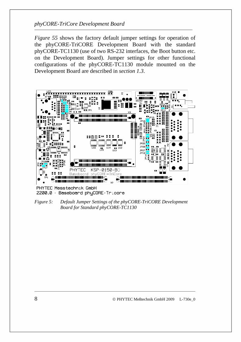
Figure 55 shows the factory default jumper settings for operation of the phyCORE-TriCORE Development Board with the standard phyCORE-TC1130 (use of two RS-232 interfaces, the Boot button etc. on the Development Board). Jumper settings for other functional configurations of the phyCORE-TC1130 module mounted on the Development Board are described in section 1.3.
8 © PHYTEC Meßtechnik GmbH 2009 L-730e_0
Figure 5: Default Jumper Settings of the phyCORE-TriCORE Development Board for Standard phyCORE-TC1130

phyCORE-TriCore Development Board
Figure 56 shows the factory default jumper settings for operation of the phyCORE-TriCORE Development Board with the standard phyCORE-TC1796 (use of two RS-232 interfaces, the Boot button etc. on the Development Board). Jumper settings for other functional configurations of the phyCORE-TC1796 module mounted on the Development Board are described in section 1.3.
© PHYTEC Meßtechnik GmbH 2009 L-730e_0 9
Figure 6: Default Jumper Settings of the phyCORE-TriCORE Development Board for Standard phyCORE-TC1796

phyCORE-TriCore Development Board
1.3 Functional Components on the phyCORE-TriCORE Development Board
This section describes the functional components of the phyCORE-TriCORE Development Board supported by the phyCORE-TC1130 or phyCORE-TC1796 and appropriate jumper settings to activate these components. Depending on the specific configuration of the phyCORE-TC1130 or phyCORE-TC1796 module, alternative jumper settings can be used. These jumper settings are different from the factory default settings shown in Figure 55 and Figure 6 and enable alternative or additional functions on the phyCORE-TriCORE Development Board depending on user needs.
1.3.1 Power Supply at X1
Caution: Do not use a laboratory adapter to supply power to the Development Board! Power spikes during power-on could destroy the phyCORE module mounted on the Development Board! Do not change modules or jumper settings while the Development Board is supplied with power! Permissible input voltage: +/-5 VDC regulated. The required current load capacity of the power supply depends on the specific configuration of the phyCORE-TC1130 or phyCORE-TC1796 mounted on the Development Board as well as whether an optional expansion board is connected to the Development Board. An adapter with a minimum supply of 1.5 A is recommended.
Figure 7: Connecting the Supply Voltage at X1
10 © PHYTEC Meßtechnik GmbH 2009 L-730e_0
+5VDC
GND
≥ 1.5 A
center hole1.3mm 3.5mm
-- +polarity:

phyCORE-TriCore Development Board
© PHYTEC Meßtechnik GmbH 2009 L-730e_0 11
1.3.2 Activating the Bootstrap Loader
The Infineon Tricore-TC1130 and TC1796 microcontroller contains an on-chip Bootstrap Loader that provides basic communication and programming functions. The combination of this Bootstrap Loader and the corresponding Flash download software installed on the PC allows for Flash programming with application code via an RS-232 interface. In order to start the on-chip Bootstrap Loader on the phyCORE-TC1130 and phyCORE-TC1796, the configuration inputs HWCFG0-3 of the microcontroller must provide a certain bit pattern at the time the Reset signal changes from its active to the inactive state. This bit pattern is created by solder jumpers on the module and pass through to the controller with the help of an electronic switch. Applying a low-level signal at pin X1C9 of the phyCORE-TC1130 or phyCORE-TC1796 (via the Boot input) activates the electronic switch. The phyCORE-TriCORE Development Board provides two different options to activate the on-chip Bootstrap Loader: 1. The Boot button (S1) can be connected to GND via Jumper JP12
which is located next the the Boot and Reset buttons at S1 and S2. This configuration enables start-up of the on-chip Bootstrap Loader if the Boot button is pressed during a hardware reset or power-on.
Jumper Setting Description
JP12 1 + 2 (default)
Boot button (in conjunction with Reset button or connection of the power supply) starts the
Bootstrap Loader on the TC1130/TC1796 Table 1: JP12 Configuration of the Boot Button

phyCORE-TriCore Development Board
12 © PHYTEC Meßtechnik GmbH 2009 L-730e_0
2. It is also possible to start the Bootstrap Loader via external signals applied to the DB-9 socket P1A. This requires control of the signal transition on the Reset line via pin 7 while a static low-level is applied to pin 4 for the Boot signal.
Jumper Setting Description
JP20 1 + 2 Pin 7 (CTS) of the DB-9 socket P1A as RESET signalfor the phyCORE-TC1130 or phyCORE-TC1796
2 + 3 Pin 7 (CTS) of the DB-9 socket P1A as BOOT signalfor the phyCORE-TC1130 or phyCORE-TC1796
open (default)
function not used
JP21 1 + 2 Pin 4 (DSR) of the DB-9 socket P1A as BOOT signalfor the phyCORE-TC1130 or phyCORE-TC1796
2 + 3 Pin 4 (DSR) of the DB-9 socket P1A as RESET signalfor the phyCORE-TC1130 or phyCORE-TC1796
open (default)
function not used
JP13 1 + 2 Low-level Boot signal connected with the BOOT input of the phyCORE-TC1130 or phyCORE-TC1796
2 + 3 Jumper setting generates high-level on Boot inputof the phyCORE-TC1130 or phyCORE-TC1796
open (default)
function not used
Table 2: JP20, JP21, JP13 Configuration of Boot via RS-232
Caution: JP20 and JP21 must have the same setting at any time: JP20,JP21 = 1+2 or JP20,JP21 = 2+3

phyCORE-TriCore Development Board
© PHYTEC Meßtechnik GmbH 2009 L-730e_0 13

phyCORE-TriCore Development Board
1.3.3 First Serial Interface at Socket P1A
Socket P1A is the lower socket of the double DB-9 connector at P1. P1A is connected via jumpers to the first serial interface of the phyCORE-TC1130 or phyCORE-TC1796. All Signals from P1A are accessible at connector X9 When connected to a host-PC, the phyCORE-TC1130 or phyCORE-TC1796 can be rendered in Bootstrap mode via signals applied to the socket P1A (refer to section 1.3.2).
Jumper Setting Description JP22 closed
(default) Pin 2 of DB-9 socket P1A connected with RS-232 interface signal TxD0 of the phyCORE-TC1130 or
phyCORE-TC1796 JP23 closed
(default) Pin 3 of DB-9 socket P1A connected with RS-232
interface signal RxD0 from the phyCORE-TC1130 or phyCORE-TC1796
Table 3: Jumper Configuration for the First RS-232 Interface
Pin 2: TxD0
Pin 3: RxD0 Pin 5: GND
Figure 8: Pin Assignment of the DB-9 Socket P1A as First RS-232 (Front View)
14 © PHYTEC Meßtechnik GmbH 2009 L-730e_0
1234
7
6
5
89

phyCORE-TriCore Development Board
1.3.4 Second Serial Interface at Socket P1B
Socket P1B is the upper socket of the double DB-9 connector at P1. P1B is connected via jumpers to the second serial interface of the phyCORE-TC1130 or phyCORE-TC1796. Handshake signals from P1A are accessible at connector X8
Jumper Setting Description JP15 closed
(default) Pin 2 of DB-9 socket P1B connected with RS-232 interface signal TxD1 of the phyCORE-TC1130 or phyCORE-TC1796
J16 closed (default)
Pin 3 of DB-9 socket P1B connected with RS-232 interface signal RxD1 from the
phyCORE-TC1130 or phyCORE-TC1796
Table 4: Jumper Configuration for the Second RS-232 Interface
Pin 2: TxD1
Pin 3: RxD1 Pin 5: GND
Figure 9: Pin Assignment of the DB-9 Socket P1A as Second RS-232 (Front View)
© PHYTEC Meßtechnik GmbH 2009 L-730e_0 15
1234
7
6
5
89

phyCORE-TriCore Development Board
1.3.5 First CAN Interface at Plug P2A
Plug P2A is the lower plug of the double DB-9 connector at P2. P2A is connected to the first CAN interface (CAN0) of the phyCORE-TC1130 or phyCORE-TC1796 via jumpers. Depending on the configuration of the CAN transceivers and their power supply, the following three configurations are possible:
1. CAN transceiver populating the phyCORE-TC1130 or phyCORE-TC1796 is enabled and the CAN signals from the module extend directly to plug P2A.
Jumper Setting Description JP25 1 + 2
(default) Pin 7 of DB-9 plug P2A connected with CAN_H0 from
on-board transceiver on the phyCORE-TC1130 or phyCORE-TC1796
JP24 1 + 2 (default)
Pin 2 of DB-9 plug P2A connected with CAN_L0 from on-board transceiver on the phyCORE-TC1130
or phyCORE-TC1796 JP14 open
(default) No supply voltage to CAN transceiver and opto-coupler
on the phyCORE-TriCORE Development Board JP19 closed
(default) GND potential at CAN transceiver and opto-coupler on
the phyCORE-TriCORE Development Board
Table 5: Jumper Configuration for CAN Plug P2A Using the CAN Transceiver on the phyCORE-TC1130 or phyCORE-TC1796
Pin 3: GND (Development Board Ground) Pin 7: CAN-H0 (not galvanically separated) Pin 2: CAN-L0 (not galvanically separated) Pin 6: GND (Development Board Ground)
Figure 10: Pin Assignment of the DB-9 Plug P2A (CAN Transceiver on
phyCORE-TC1130, Front View)
16 © PHYTEC Meßtechnik GmbH 2009 L-730e_0
1234
7
6
5
89

phyCORE-TriCore Development Board
2. The CAN transceiver populating the phyCORE-TC1130 or phyCORE-TC1796 is disabled; CAN signals generated by the CAN transceiver (U3) on the Development Board extending to connector P2A without galvanic seperation:
Jumper Setting Description
JP25 1 + 3 2 + 4
Pin 7 of DB-9 plug P2A connected with CAN-H0 from CAN transceiver U5 on the Development Board
JP24 1 + 3 2 + 4
Pin 2 of DB-9 plug P2A connected with CAN-L0 from CAN transceiver U5 on the Development Board
JP14 2 + 3 Supply voltage for CAN transceiver and opto-coupler derived from local supply circuitry on the phyCORE-TriCORE Development Board
JP19 closed CAN transceiver and opto-coupler on the Development Board connected with local GND potential
Table 6: Jumper Configuration for CAN Plug P2A Using the CAN Transceiver on the Development Board
Pin 3: GND (Development Board Ground) Pin 7: CAN-H0 (not galvanically separated) Pin 2: CAN-L0 (not galvanically separated) Pin 6: GND (Development Board Ground
Figure 11: Pin Assignment of the DB-9 Plug P2A (CAN Transceiver on Development Board)
© PHYTEC Meßtechnik GmbH 2009 L-730e_0 17
1234
7
6
5
89

phyCORE-TriCore Development Board
3. The CAN transceiver populating the phyCORE-TC1130 or phyCORE-TC1796 is disabled; CAN signals generated by the CAN transceiver (U3) on the Development Board extend to connector P2A with galvanic separation. This configuration requires connection of an external CAN supply voltage of 7 to 13 V. The external power supply must be only connected to either P2A or P2B.
Jumper Setting Description JP25 1 + 3
2 + 4 Pin 7 of DB-9 plug P2A connected with CAN-H0 from
CAN transceiver U5 on the Development Board JP24 1 + 3
2 + 4 Pin 2 of DB-9 plug P2A connected with CAN-L0 from
CAN transceiver U5 on the Development Board JP14 1 + 2 Supply voltage for CAN transceiver and opto-coupler
on the Development Board derived from external source (CAN bus) via on-board voltage regulator
JP19 open CAN transceiver and opto-coupler on the Development Board disconnected from local GND potential
Table 7: Jumper Configuration for CAN Plug P2A Using the CAN Transceiver on the Development Board with Galvanic Separation
Pin 9: VCAN+
Pin 3: VCAN- Pin 7: CAN-H0 (galvanically separated) Pin 2: CAN-L0 (galvanically separated) Pin 6: VCAN-
Figure 12: Pin Assignment of the DB-9 Plug P2A (CAN Transceiver on Development Board with Galvanic Separation)
18 © PHYTEC Meßtechnik GmbH 2009 L-730e_0
1234
7
6
5
89
phyCORE-TriCore Development Board
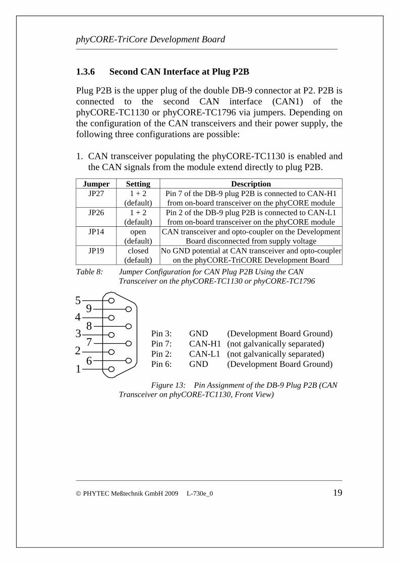
1.3.6 Second CAN Interface at Plug P2B
Plug P2B is the upper plug of the double DB-9 connector at P2. P2B is connected to the second CAN interface (CAN1) of the phyCORE-TC1130 or phyCORE-TC1796 via jumpers. Depending on the configuration of the CAN transceivers and their power supply, the following three configurations are possible: 1. CAN transceiver populating the phyCORE-TC1130 is enabled and
the CAN signals from the module extend directly to plug P2B.
Jumper Setting Description JP27 1 + 2
(default) Pin 7 of the DB-9 plug P2B is connected to CAN-H1 from on-board transceiver on the phyCORE module
JP26 1 + 2 (default)
Pin 2 of the DB-9 plug P2B is connected to CAN-L1 from on-board transceiver on the phyCORE module
JP14 open (default)
CAN transceiver and opto-coupler on the Development Board disconnected from supply voltage
JP19 closed (default)
No GND potential at CAN transceiver and opto-coupler on the phyCORE-TriCORE Development Board
Table 8: Jumper Configuration for CAN Plug P2B Using the CAN Transceiver on the phyCORE-TC1130 or phyCORE-TC1796
Pin 3: GND (Development Board Ground) Pin 7: CAN-H1 (not galvanically separated) Pin 2: CAN-L1 (not galvanically separated) Pin 6: GND (Development Board Ground) Figure 13: Pin Assignment of the DB-9 Plug P2B
Transceiver on phyCORE-TC113 (CAN
0, Front View)
© PHYTEC Meßtechnik GmbH 2009 L-730e_0 19
1234
7
6
5
89

phyCORE-TriCore Development Board
2. The CAN transceiver populating the phyCORE-TC1130 or phyCORE-TC1796 is disabled; CAN signals generated by the CAN transceiver (U4) on the Development Board extending to connector P2B without galvanic seperation:
Jumper Setting Description JP27 1 + 3
2 + 4 Pin 7 of DB-9 plug P2B connected with CAN-H1 from
CAN transceiver U4 on the Development Board JP26 1 + 3
2 + 4 Pin 2 of DB-9 plug P2B connected with CAN-L1 from
CAN transceiver U4 on the Development Board JP14 2 + 3 Supply voltage for CAN transceiver and opto-coupler
derived from local supply circuitry on the phyCORE-TriCORE Development Board
JP19 closed CAN transceiver and opto-coupler on the Development Board connected with local GND potential
Table 9: Jumper Configuration for CAN Plug P2B Using the CAN Transceiver on the Development Board
Pin 3: GND (Development Board Ground) Pin 7: CAN-H1 (not galvanically separated) Pin 2: CAN-L1 (not galvanically separated) Pin 6: GND (Development Board Ground
Figure 14: Pin Assignment of the DB-9 Plug P2B (CAN Transceiver on Development Board)
20 © PHYTEC Meßtechnik GmbH 2009 L-730e_0
1234
7
6
5
89

phyCORE-TriCore Development Board
3. The CAN transceiver populating the phyCORE-TC1130 or phyCORE-TC1796 is disabled; CAN signals generated by the CAN transceiver (U4) on the Development Board extend to connector P2B with galvanic separation. This configuration requires connection of an external CAN supply voltage of 7 to 13 V. The external power supply must be only connected to either P2A or P2B.
Jumper Setting Description
JP27 1 + 3 2 + 4
Pin 7 of DB-9 plug P2B connected with CAN-H1 from CAN transceiver U3 on the Development Board
JP26 1 + 3 2 + 4
Pin 2 of DB-9 plug P2B connected with CAN-L1 from CAN transceiver U3 on the Development Board
JP14 1 + 2 Supply voltage for CAN transceiver and opto-coupler on the Development Board derived from external source
(CAN bus) via on-board voltage regulator JP19 open CAN transceiver and opto-coupler on the Development
Board disconnected from local GND potential
Table 10: Jumper Configuration for CAN Plug P2B Using the CAN Transceiver on the Development Board with Galvanic Separation
Pin 9: VCAN+
Pin 3: VCAN- Pin 7: CAN-H1 (galvanically separated) Pin 2: CAN-L1 (galvanically separated) Pin 6: VCAN-
Figure 15: Pin Assignment of the DB-9 Plug P2B (CAN Transceiver on Development Board with Galvanic Separation)
© PHYTEC Meßtechnik GmbH 2009 L-730e_0 21
1234
7
6
5
89

phyCORE-TriCore Development Board
22 © PHYTEC Meßtechnik GmbH 2009 L-730e_0
1.3.7 RJ45 Ethernet Connector X7
The phyCORE-TriCORE Development Board provides the Ethernet RJ45 jack with integrated magnetic at X7 to enable immediate connection of the phyCORE-TC1130 or phyCORE-TC1796 to an 10/100 Mbit/s Ethernet network. Two status LEDs for LINK and LAN are provided to display network status. The following jumper settings are required:
Jumper Setting Description JP10 1 + 2
3 + 4 5 + 6 7 + 8
The Ethernet transformer module is connected to the Ethernet signals on the phyCORE-TC1130 or
phyCORE-TC1796
JP2 open configuration for phyCORE-TC1130 module closed configuration for phyCORE-TC1796 module
JP3, JP4, open configuration for phyCORE-TC1796 and phyCORE-TC1796
JP5, JP6 open configuration for phyCORE-TC1130 module closed configuration for phyCORE-TC1796 module
JP11 1+2 configuration for phyCORE-TC1796 module 2+3 configuration for phyCORE-TC1130 module
Table 11: JP2-6 ,JP10,JP11, Configuration of the Ethernet Interface
1.3.8 Programmable LED D3
The phyCORE-TriCORE Development Board offers a programmable LED at D5 for user implementations. This LED can be connected to port pin P2.11 of the phyCORE-TC1130 or P8.0 of the phyCORE-TC1796 which is available via signal GPIO0 (JP18 = closed). A low-level at port pin causes the LED to illuminate, LED D5 remains off when writing a high-level to the appropriate port pin.
Jumper Setting Description JP18 closed Port pin P2.11 (GPIO0) of the TC1130 controller
controls LED D5 on the Development Board closed Port pin P8.0 (GPIO0) of the TC1130 controller
controls LED D5 on the Development Board
Table 12: JP18 Configuration of the Programmable LED D3

phyCORE-TriCore Development Board
© PHYTEC Meßtechnik GmbH 2009 L-730e_0 23
1.3.9 Pin Assignment Summary of the phyCORE, the Expansion Bus and the Patch Field
As described in section 1.1, all signals from the phyCORE-TC1130 or phyCORE-TC1796 extend in a strict 1:1 assignment to the Expansion Bus connector X2 on the Development Board. These signals, in turn, are routed in a similar manner to the patch field on an optional expansion board that mounts to the Development Board at X2. Please note that, depending on the design and size of the expansion board, only a portion of the entire patch field is utilized under certain circumstances. When this is the case, certain signals described in the following section will not be available on the expansion board. However, the pin assignment scheme remains consistent. A two dimensional numbering matrix similar to the one used for the pin layout of the phyCORE-connector is provided to identify signals on the Expansion Bus connector (X2 on the Development Board) as well as the patch field.

phyCORE-TriCore Development Board
However, the numbering scheme for Expansion Bus connector and patch field matrices differs from that of the phyCORE-connector, as shown in the following two figures:
B A
D C
80
1
80
1
Figure 16: Pin Assignment Scheme of the Expansion Bus
A B C D E F
54
1
24 © PHYTEC Meßtechnik GmbH 2009 L-730e_0
Figure 17: Pin Assignment Scheme of the Patch Field

phyCORE-TriCore Development Board
© PHYTEC Meßtechnik GmbH 2009 L-730e_0 25
The pin assignment on the phyCORE-TC1130 and phyCORE-TC1796 , in conjunction with the Expansion Bus (X2) on the Development Board and the patch field on an expansion board, is as follows: Signal phyCORE TC1130
Signal phyCORE TC1796
phyCORE-TC1130 phyCORE-TC1796
Expansion Bus Patch Field
xD0 D0 18B 18B 33F xD1 D1 19A 19A 34A xD2 D2 20A 20A 34E xD3 D3 20B 20B 34B xD4 D4 21A 21A 34D xD5 D5 21B 21B 34F xD6 D6 22B 22B 35A xD7 D7 23A 23A 35E xD8 D8 28B 28B 37C xD9 D9 29A 29A 37E xD10 D10 30A 30A 37B xD11 D11 30B 30B 37F xD12 D12 31A 31A 38A xD13 D13 31B 31B 38C xD14 D14 32B 32B 38E xD15 D15 33A 33A 38B xD16 D16 37B 37B 40A xD17 D17 38A 38A 40E xD18 D18 38B 38B 40B xD19 D19 39A 39A 40D xD20 D20 40A 40A 40F xD21 D21 40B 40B 41A xD22 D22 41A 41A 41E xD23 D23 41B 41B 41B xD24 D24 42B 42B 41F xD25 D25 43A 43A 42A xD26 D26 43B 43B 42C xD27 D27 44A 44A 42E xD28 D28 45A 45A 42B xD29 D29 45B 45B 42F xD30 D30 46A 46A 43A xD31 D31 46B 46B 43C

phyCORE-TriCore Development Board
26 © PHYTEC Meßtechnik GmbH 2009 L-730e_0
Signal phyCORE TC1130
Signal phyCORE TC1796
phyCORE-TC1130 phyCORE-TC1796
Expansion Bus Patch Field
xA0 A0 8B 8B 30B xA1 A1 9A 9A 30D xA2 A2 10A 10A 30F xA3 A3 10B 10B 31A xA4 A4 11A 11A 31E xA5 A5 11B 11B 31B xA6 A6 12B 12B 31F xA7 A7 13A 13A 31A xA8 A8 13B 13B 32C xA9 A9 14A 14A 32E xA10 A10 15A 15A 32B xA11 A11 15B 15B 32F xA12 A12 16A 16A 33A xA13 A13 16B 16B 33C xA14 A14 17B 17B 33E xA15 A15 18A 18A 33B xA16 A16 23B 23B 35B xA17 A17 24A 24A 35D xA18 A18 25A 25A 35F xA19 A19 25B 25B 36A xA20 A20 26A 26A 36E xA21 A21 26B 26B 36B xA22 A22 27B 27B 36F xA23 A23 28A 28A 37A
Table 13: Pin Assignment for the phyCORE-TC1130, phyCORE-TC1796 and Development Board / Expansion Board

phyCORE-TriCore Development Board
© PHYTEC Meßtechnik GmbH 2009 L-730e_0 27
Signal phyCORE TC1130
Signal phyCORE TC1796
phyCORE-TC1130 phyCORE-TC1796
Expansion Bus Patch
P00 P82 / FCLP1A
13C 13C 4F
P01 P83 / SON0
13D 13D 5A
P03 P84 / FCLN1 14C 14C 5C P02 P85 / SOP1A 15C 15C 5E P04 P86 / SON0 15D 15D 5B P05 /HOLD 35B 35B 39B P06 /HLDA 36A 36A 39D P07 /BREQ 36B 36B 39F P08 P10 2B 2B 28E P09 P11 3A 3A 28B P010 P12 3B 3B 28F P011 /CS1 6B 6B 29F P10 AN9 / P09 74C 74C 25C P11 AN11 / P011 73C 73C 24F P12 AN10 / P010 73D 73D 25A P13 AN12 / P012 72D 72D 24B P14 AN14 / P014 71C 71C 24A P15 AN13 / P013 71D 71D 24E P16 AN16 / P40 70C 70C 23D P17 AN15 / P015 70D 70D 23F P18 AN17 / P41 69C 69C 23B P19 AN19 / P43 68C 68C 23A P110 AN18 / P42 68D 68D 23E P111 AN20 / P44 67D 67D 22F P112 AN22 / P46 66C 66C 22B P113 AN21 / P45 66D 66D 22D P114 AN24 / P48 65C 65C 22A P115 AN23 / P47 65D 65D 22E P20 / RxD0_TTL
P50 / RxD0_TTL
16D 16D 6A
P21 / TxD0_TTL
P51 / TxD0_TTL
17D 17D 6C
P22 / MRST0 MRST0 27D 27D 9B

phyCORE-TriCore Development Board
28 © PHYTEC Meßtechnik GmbH 2009 L-730e_0
Signal phyCORE TC1130
Signal phyCORE TC1796
phyCORE-TC1130 phyCORE-TC1796
Expansion Bus Patch Field
P23 / MTSR0 MTSR0 28D 28D 10A P24 / SCLK0 SCLK0 30D 30D 10B P25 / MRST1 P65 / MRST1 26C 26C 9A P26 / MTSR1 P64 / MTSR1 28C 28C 9F P27 / SCLK1 P66 / SCLK1 29C 29C 10C P28 / RxD1_TTL
P52 / RxD1_TTL
19C 19C 6F
P29 / TxD1_TTL
P53 / TxD1_TTL
20C 20C 7A
P210 P81 / SOP0A 12D 12D 4B P211 P80 /
FCLP0A 11D 11D 4A
P212 / SDA0 SDA0 32D 32D 11C P213 / SCL0 SCL0 31C 31C 10F P214 / SDA1 SDA1 24C 24C 8B P215 / SCL1 SCL1 25C 25C 8D P30 P75 50D 50D 17E P31 P76/
AD1EMUX0 51C 51C 17B
P32 P77/ AD1EMUX1
51D 51D 17D
P33 AN43 52D 52D 17F P34 AN41 / P57 53C 53C 18A P35 AN42 53D 53D 18E P36 AN40 / P98 54C 54C 18B P37 AN38 / P96 55C 55C 18D P38 AN39 / P97 55D 55D 18F P39 AN36 / P94 56C 56C 19A P310 AN37 / P95 56D 56D 19E P311 AN35 / P93 57D 57D 19B P312 AN33 / P91 58C 58C 19F P313 AN34 / P92 58D 58D 20A P314 AN32 / P90 59C 59C 20C P315 AN31 / P415 60C 60C 20E P40 / USBCLK
P55 46C 46C 15F
P41 / RVCI P56 46D 46D 16A

phyCORE-TriCore Development Board
© PHYTEC Meßtechnik GmbH 2009 L-730e_0 29
Signal phyCORE TC1130
Signal phyCORE TC1796
phyCORE-TC1130 phyCORE-TC1796
Expansion Bus Patch Field
P42 / VPI P70 47D 47D 16C P43 / VMI P71/
AD0EMUX2 48C 48C 16E
P44 / VPO P72/ AD0EMUX0
48D 48D 16B
P45 / VMO P73/ AD0EMUX1
49C 49C 16F
P46 / USBOE P74 50C 50C 17A P47 / /BRKOUT_A
/BRKOUT 40C 40C 13D
Table 14: Pin Assignment for the phyCORE-TC1130, phyCORE-TC1796 and Development Board / Expansion Board

phyCORE-TriCore Development Board
30 © PHYTEC Meßtechnik GmbH 2009 L-730e_0
Signal phyCORE TC1130
Signal phyCORE TC1796
phyCORE-TC1130 phyCORE-TC1796
Expansion Bus Patch Field
EGPIO0 P23 / SLSO3 80A 80A 54E EGPIO1 P22 / SLSO2 80B 80B 54B EGPIO3 P26 / SLSO6 78A 78A 53B EGPIO2 P24 / SLSO4 79A 79A 54A EGPIO4 P25 / SLSO5 78B 78B 53F EGPIO5 P27 / SLSO7 77B 77B 53E EGPIO6 P29 76A 76A 53A EGPIO7 P28 76B 76B 53C EGPIO8 P211 75A 75A 52B EGPIO9 P210 75B 75B 52F EGPIO11 P214 73A 73A 52A EGPIO10 P212 74A 74A 52E EGPIO12 P213 73B 73B 52C EGPIO13 P215 72B 72B 51F EGPIO14 P31 71A 71A 51E EGPIO15 P30 71B 71B 51B EGPIO16 P33 70A 70A 50F EGPIO17 P32 70B 70B 51A EGPIO18 P34 69A 69A 50D EGPIO19 P36 68A 68A 50E EGPIO20 P35 68B 68B 50B EGPIO21 P37 67B 67B 50A EGPIO22 P39 66A 66A 49D EGPIO23 P38 66B 66B 49F
EGPIO24 P311 65A 65A 49E EGPIO25 P310 65B 65B 49B EGPIO26 P312 64A 64A 49A EGPIO27 P314 63A 63A 48B EGPIO28 P313 63B 63B 48F EGPIO29 P315 62B 62B 48E EGPIO30 P14 61A 61A 48A EGPIO31 P13 61B 61B 48C

phyCORE-TriCore Development Board
© PHYTEC Meßtechnik GmbH 2009 L-730e_0 31
Signal phyCORE TC1130
Signal phyCORE TC1796
phyCORE-TC1130 phyCORE-TC1796
Expansion Bus Patch Field
EGPIO32 P16 60A 60A 47B EGPIO33 P15 60B 60B 47F EGPIO34 P17 59A 59A 47E EGPIO35 P18 58A 58A 47A EGPIO36 P19 58B 58B 47C EGPIO37 P110 57B 57B 46F EGPIO38 P111 56A 56A 46E EGPIO39 P112 56B 56B 46B EGPIO40 P113 55A 55A 45F
Table 15: Pin Assignment for the phyCORE-TC1130, phyCORE-TC1796 and Development Board / Expansion Board
Signal phyCORE TC1130
Signal phyCORE TC1796
phyCORE-TC1130 phyCORE-TC1796
Expansion Bus Patch Field
REFA VAREF0 80D 80D 27E ADC0 AN0 / P00 80C 80C 27A ADC1 AN1 / P01 79C 79C 26F ADC2 AN2 / P02 78D 78D 26B ADC3 AN3 / P03 78C 78C 26E ADC4 AN4 / P04 77D 77D 26C ADC5 AN5 / P05 76D 76D 26A ADC6 AN6 / P06 76C 76C 25F ADC7 AN7 / P07 75D 75D 25B DAC0 AN8 / P08 75C 75C 25E

phyCORE-TriCore Development Board
32 © PHYTEC Meßtechnik GmbH 2009 L-730e_0
Signal phyCORE TC1130
Signal phyCORE TC1796
phyCORE-TC1130 phyCORE-TC1796
Expansion Bus Patch Field
/HDRST /HDRST 10C 10C 3D /PORESET /PORST 11C 11C 4E /NMI /NMI 4A 4A 29A /TRST /TRST 41C 41C 14A TCK TCK 43D 43D 15A TDI TDI 40D 40D 13F TDO TDO 41D 41D 14E TMS TMS 42D 42D 14B /TRCLK /TRCLK 38C 38C 13A /BRKIN /BRKIN 39C 39C 13B xHWCFG2 AN29 / P413 61D 61D 21A xHWCFG1 AN30 / P414 61C 61C 20F xHWCFG0 VAREF1 60D 60D 20B MII_TXCLK AN25 / P49 64C 64C 21F MII_RXCLK AN26 / P410 63D 63D 21B MII_MDIO AN28 / P412 62D 62D 21C /E_INT 5V_VBUS 30C 30C 10E E_DUPLEX P54 25D 25D 8F E_NWAYEN /SLSI0 26D 26D 9E x/CS3 /CS3 5A 5A 29E x/CS2 /CS2 5B 5B 29B /CSCOMB /CSCOMB 47B 47B 43E x/BC0 /BC0 8A 8A 30E x/BC1 /BC1 33B 33B 38F x/BC2 /BC2 52B 52B 45A x/BC3 /BC3 53B 53B 45B x/RD /RD 7B 7B 30A x/WR /WR 49A 49A 44A xALE /ADV 6A 6A 29D x/BAA /BAA 51B 51B 44F xADV /ADV 50B 50B 44B x/WAIT /WAIT 34A 34A 39A

phyCORE-TriCore Development Board
© PHYTEC Meßtechnik GmbH 2009 L-730e_0 33
Signal phyCORE TC1130
Signal phyCORE TC1796
phyCORE-TC1130 phyCORE-TC1796
Expansion Bus Patch Field
/RESIN /RESIN 10D 10D 3F /BOOT /BOOT 9C 9C 3B FL_VPEN /CS0 35A 35A 39E xMR / W MR / W 48B 48B 43F xBFCLKI BFCLKI 50A 50A 44E xBFCLKO BFCLKO 51A 51A 44D
Table 16: Pin Assignment for the phyCORE-TC1130, phyCORE-TC1796 and Development Board / Expansion Board
Signal phyCORE TC1130
Signal phyCORE TC1796
phyCORE-TC1130 phyCORE-TC1796
Expansion Bus Patch Field
CAN_H0 CAN_H0 21D 21D 7D CAN_L0 CAN_L0 20D 20D 7E CAN_H1 CAN_H1 18C 18C 6E CAN_L1 CAN_L1 18D 18D 6B CAN_H2 CAN_H2 44C 44C 15C CAN_L2 CAN_L2 43C 43C 14F CAN_H3 CAN_H3 45D 45D 15B CAN_L3 CAN_L3 45C 45C 15E RXD0 RXD0 22D 22D 7F TXD0 TXD0 23D 23D 8E RXD1 RXD1 21C 21C 7B TXD1 TXD1 23C 23C 8A ETH_Link LED
ETH_Link LED
33C 33C 11E
ETH_Lan LED
ETH_Lan LED
34C 34C 11F
ETH_RXD- ETH_RXD- 35C 35C 12A ETH_TXD- ETH_TXD- 36C 36C 12B ETH_RXD+ ETH_RXD+ 35D 35D 12E ETH_TXD+ ETH_TXD+ 36D 36D 12D D+ D+ 37D 37D 12F D- D- 38D 38D 13E
Table 17: Pin Assignment for the phyCORE-TC1130, phyCORE-TC1796 and Development Board / Expansion Board
Signal Signal phyCORE-TC1130 Expansion Bus Patch Field

phyCORE-TriCore Development Board
34 © PHYTEC Meßtechnik GmbH 2009 L-730e_0
phyCORE TC1130
phyCORE TC1796
phyCORE-TC1796
RTC_ CLKOUT
RTC_ CLKOUT
1B 1B 28C
/IRTC /IRQRTC 33D 33D 11B Tout NC 8D 8D 3A
Table 18: Pin Assignment for the phyCORE-TC1130, phyCORE-TC1796 and Development Board / Expansion Board
Signal phyCORE TC1130
Signal phyCORE TC1796
phyCORE-TC1130 phyCORE-TC1796
Expansion Bus Patch Field
3V3_IN 3V3 1C, 2C, 1D, 2D 1C, 2C, 1D, 2D 1A, 1C 1V5_IN NC 4C, 5C not connected to
Expansion Bus
4C, 5C = 5V 2A, 1B VBAT_IN VBAT_IN 6C 6C 2B GND 2A, 7A, 12A, 17A,
22A, 27A, 32A, 37A, 42A, 47A, 52A, 57A, 62A, 67A, 72A, 77A, 4B, 9B, 14B, 19B, 24B, 29B, 34B, 39B, 44B, 49B, 54B, 59B, 64B, 69B, 74B, 79B, 3C, 7C, 12C, 17C, 22C, 27C, 32C, 37C, 42C, 47C, 52C, 57C, 62C, 67C, 72C, 3D, 9D, 14D, 19D, 24D, 29D, 34D, 39D, 44D, 49D, 54D, 59D, 64D, 69D,
2A, 7A, 12A, 17A, 22A, 27A, 32A, 37A, 42A, 47A, 52A, 57A, 62A, 67A, 72A, 77A, 4B, 9B, 14B, 19B, 24B, 29B, 34B, 39B, 44B, 49B, 54B, 59B, 64B, 69B, 74B, 79B, 3C, 7C, 12C, 17C, 22C, 27C, 32C, 37C, 42C, 47C, 52C, 57C, 62C, 67C, 72C, 3D, 9D, 14D, 19D, 24D, 29D, 34D, 39D, 44D, 49D, 54D, 59D, 64D, 69D,
3C, 4C, 7C, 8C, 9C, 12C, 13C, 14C, 17C, 18C, 19C, 22C, 23C, 24C, 27C, 29C, 30C, 31C, 34C, 35C, 36C, 39C, 40C, 41C, 44C, 45C, 46C, 49C, 50C, 51C, 54C, 4D, 5D, 6D, 9D, 10D, 11D, 14D, 15D, 16D, 19D, 20D, 21D, 24D, 25D, 26D, 28D, 31D, 32D, 33D, 36D, 37D, 38D, 41D, 42D, 43D, 46D, 47D, 48D, 51D, 52D, 53D, 1E, 2E, 1F
AGND 77C, 74D, 79D 77C, 74D, 79D GND
Table 19: Pin Assignment Power Supply for the phyCORE-TC1130 / Development Board / Expansion Board

phyCORE-TriCore Development Board
© PHYTEC Meßtechnik GmbH 2009 L-730e_0 35
Signal phyCORE TC1130
Signal phyCORE TC1796
phyCORE-TC1130 phyCORE-TC1796
Expansion Bus Patch Field
PLD_TMS LAN_/CS (W5300)
48A 48A 43B
PLD_TCK /CS_RAM2 53A 53A 45E PLD_TDO P115 54A 54A 45D PLD_TDI P114 55B 55B 46A SPIEEPWP P87 16C 16C 5F ICCEEPWP AN27 / P411 63C 63C 21E NC NC 1A, 4D,5D, 6D, 7D 1A, 4D,5D, 6D,
7D 28A,2C,1D, 2D,2F
Table 20: Pin Assignment for the phyCORE-TC1130, phyCORE-TC1796 and Development Board / Expansion Board

phyCORE-TriCore Development Board
1.3.10 DS2401 Silicon Serial Number
Communication to a DS2401 Silicon Serial Number can be implemented in various software applications for the definition of a node address or as copy protection in networked applications. The DS2401 is optionally populated on U2 on the Development Board.
The Silicon Serial Number Chip mounted on the phyCORE-TriCORE Development Board can be connected to port pin P2.10 of the TC1130 or port pin P8.0 of the TC1796.
Jumper Setting Description JP1 closed Port pin P2.10 of the TC1130
is used to access the Silicon Serial Number JP1 closed Port pin P8.1 of the TC1796
is used to access the Silicon Serial Number Table 21: JP1 Jumper Configuration for Silicon Serial Number Chip
Figure 18: Connection of the DS2401 Silicon Serial Number
36 © PHYTEC Meßtechnik GmbH 2009 L-730e_0
not
connected GPIO Port NUMPORT
JP1

phyCORE-TriCore Development Board
© PHYTEC Meßtechnik GmbH 2009 L-730e_0 37
1.3.11 Pin Header Connectors X10
Connector X10 supplies 5 VDC at pin 1 and provides the phyCORE-TriCORE Development Board GND potential at pin 2. The maximum current draw depends on the power adapter used. 1.3.12 USB Wiggler connector X11
The phyCORE-TriCORE Development Board provides the USB jack X11 to enable access to the JTAG of the phyCORE-TC1130 or phyCORE-TC1796 via the DAS Server JTAG over USB Chip. Make sure the Latest DAS released is installed on your PC. Please contact your prefered debug vendor for support of DAS. If DAS is installed on the PC, the driver for the USB Wiggler will automatically be installed after connecting the The phyCORE -TriCORE Development Board with the PC. Two status LEDs for USB Wiggler status are provided: LED D4 (green): LED is ON if a working connection is established with the DAS Server on the PC LED D6 (red): LED is ON when DAS Server is disconnected after
being connected Caution: When using USB Wiggler connector X11, make sure there is NO or tristated connection on the JTAG connector of the phyCORE-TC1130 (X2) or phyCORE-TC1796 (X1) and the OCDS2 connector phyCORE-TriCORE Development Board is NOT used

phyCORE-TriCore Development Board
38 © PHYTEC Meßtechnik GmbH 2009 L-730e_0
1.3.13 LCD connector
The connector LCD on the phyCORE-TriCORE Development Board enable connection of an optional LCD – Display. Signals for the following Display-Controller are provided T6963C (default) , HD61202, HD44780 Depending on the used LCD controller the following jumper configuration are required:
Jumper Setting Description JP30 2+3
(default) connect /RD signal of TC1130 or TC1796 to Pin5
of LCD connector JP31 2+3
(default) connect /WR signal of TC1130 or TC1796 to Pin6
of LCD connector JP32 1+2
(default) connect /CS signal of TC1130 or TC1796 to Pin6
of LCD connector JP36 1+2 select /CS0 for LCD ( TC1796 only)
3+4 select /CS1 for LCD ( TC1796 only) 5+6 select /CS2 for LCD 7+8 select /CS3 for LCD open
(default) No chipselect is used for display
Note the caution on bottom of this page regarding J36
JP34 1+2 Connect 5V to Pin22 of LCD connector 2+3 Connect GND to Pin22 of LCD connector
JP35 1+2 Connect 5V to Pin23 of LCD connector 2+3 Connect GND to Pin23 of LConD cnector
Table 22: Jumper Configuration for T6963C LCD-Controller Caution: J36 must be left open as long no free chip select is provided by the phyCORE-TC1130 or phyCORE-TC1796 HW-configuration On standard phyCORE-TC1796 no /CSx is free=> JP36 = open On standard phyCORE-TC1130 only /CS2 is free => JP36 = 5+6 When setting JP36, only selection of one /CSx for the LCD is allowed

phyCORE-TriCore Development Board
© PHYTEC Meßtechnik GmbH 2009 L-730e_0 39
Jumper Setting Description JP30 1+2 connect (A3 +/CSx) signal of TC1130 or TC1796 to
Pin5 of LCD connector
JP31 1+2 connect (/A+/CSx) signal of TC1130 or TC1796 to Pin6 of LCD connector
JP32 2+3 connect LCD_EN signal of TC1130 or TC1796 to Pin6
of LCD connector JP36 1+2 select /CS0 for LCD ( TC1796 only)
3+4 select /CS1 for LCD ( TC1796 only) 5+6 select /CS2 for LCD 7+8 select /CS3 for LCD
Table 23: Jumper Configuration for HD61202, HD44780 LCD-Controller Control Signals for the supported LCD-controller are: - Adressline A1 is used for R/W Signal for the HD61202, HD44780 - Adressline A2 is used for C/D Signal für the T6963C and (D/I) for HD61202 and HD44780 LCD-Controller - Adressline A3 is used for CS_LS Signal für the HD61202 - Adressline /A3 is used für for CS_RS Signal für the HD61202
-5 V negative contrast voltage
from U17
5 V contrast voltage from Dev. Board
negative contrast voltage from LCD
(default) (default for AC049)
R53= 4k7 R54= 15k R53 = 0R RT4= 5k RT4= 5k RT4 = 5k R59= 0R R56= 0R R56 = 4k7 R58= 0R R58= 0R R58 = 0R
Table 24: contrast Configuration LCD Please contact PHYTEC for information of available LCD-Displays for the phyCORE-TriCORE Development Board

phyCORE-TriCore Development Board
40 © PHYTEC Meßtechnik GmbH 2009 L-730e_0
1.3.14 JTAG PLD connector only for phyCORE-TC1130
As shon in Table 26 the 6 Pin connector JTAG_PLD provides all signals for connection of a PLD-Programmer. to load software to the onboard PLD of the phyCORE-TC1130 JTAG_PLD Signal
Pin1 3,3V Pin2 PLD_TDO Pin3 PLD_TDI Pin4 PLD_TMS Pin5 GND Pin6 PLD_TCK
Table 25: Pin assignemt JTAG_PLD connector for phyCORE- TC1130
Caution: JTAG_PLD connector on the Development board must not be used when using the phyCORE-TC1796 module on the phyCORE-TriCORE Development Board.

phyCORE-TriCore Development Board
© PHYTEC Meßtechnik GmbH 2009 L-730e_0 41
1.3.15 USB connector X12
Depending on the used phyCORE-module on the Development Board, the USB connector X12 provides the following connection. For the phyCORE-TC1130: X12 enables the connection to the
TC1130 USB feature For the phyCORE-TC1130 the following jumper settings are required:
Jumper Setting Description JP9 Open Disconnect 5V from USB Bus JP28 2+3
Table 26: Jumper Configuration for X12 USB connector for phyCORE-TC1130 For the phyCORE-TC1796: X12 enables the connection to the
TC1796 onboard USB to UART Bridge.
For the phyCORE-TC1796 the following jumper settings are required:
Jumper Setting Description JP9 Closed configuration for phyCORE-TC1796 module JP28 open configuration for phyCORE-TC1796 module
Table 27: Jumper Configuration for X12 USB connector for phyCORE-TC1796 Caution: USB to UART Bridge can not be used with the standard phyCORE TC1796 module, due to the module HW-configuration.

phyCORE-TriCore Development Board
42 © PHYTEC Meßtechnik GmbH 2009 L-730e_0
1.3.16 OCDS2 connector only for phyCORE-TC1796
OCDS2 debugging requires additional Trace Signals of the CPU with the OCDS1 Signals. With phyCORE-TriCORE Development Board, a 60 Pin Highspeed connector OCDS2, both signals are available. Caution: When using OCDS2 Trace connector OCDS2 on the phyCORE-TriCORE Development Board , make sure there is NO or tristated connection on the JTAG connector of the phyCORE-TC1130 (X2) or phyCORE-TC1796 (X1) and X11 must NOT be connected with the PC

Appendice A
© PHYTEC Meßtechnik GmbH 2009 L-730e_0 43
2 Revision History
Date Version numbers
Changes in this manual
12-March-2009 Manual L-730e_0 KSP-0150-B0 PCB# 2200.0-001
Preliminary edition.

phyCORE-TriCore Development Board
44 © PHYTEC Meßtechnik GmbH 2009 L-730e_0
Appendice A
A.1 Release Notes
The following paragraph describes the differences between the technical facts provided in this manual and the currently available hardware revisions.

Index
© PHYTEC Meßtechnik GmbH 2009 L-730e_0 45
Index
B Bootstrap Loader 11
C Concept of the Development
Board 3 Connector X4 36
D Development Board Connectors
and Jumpers 5 DS2401 35
E EMC 1 Expansion Bus 22
F First CAN Interface 15 First Serial Interface 13 Functional Components on the
phyCORE Development Board 10
J JP17 21 Jumper Configuration 7
L LED D3 21
P Patch Field 22 Pin Assignment 22 Plug P2A 15 Plug P2B 18 Power Supply 10
R Release Notes 43 RJ45 21
S Second CAN Interface 18 Second Serial Interface 14 Silicon Serial Number 35 Socket P1A (First RS-232) 13 Socket P1B (Second RS-232) 14
X X7 21

phyCORE-TriCore Development Board
46 © PHYTEC Meßtechnik GmbH 2009 L-730e_0
Document: phyCORE-TriCORE Development Board Document number: L-730e_0, Mar 2009 How would you improve this manual? Did you find any mistakes in this manual? page Submitted by: Customer number: Name: Company: Address: Return to: PHYTEC Technologie Holding AG Postfach 100403 D-55135 Mainz, Germany Fax : +49 (6131) 9221-33

Published by
© PHYTEC Meßtechnik GmbH 2009 Ordering No. L-730e_0 Printed in Germany


