n - Type Doping of Diamond Satoshi Koizumi, 1 Mariko Suzuki 2 and Julien Pernot 3 1 National Institute for Materials Science, 1 - 1 Namiki, Tsukuba 305 - 0044, Japan 2 Corporate Research & Development Center, Toshiba Corporation, 1 Komukai Toshiba - cho, Saiwai - ku, Kawasaki 212 - 8582, Japan 3 Institut NEEL, CNRS & Universit é Joseph Fourier, BP 166, F - 38042 Grenoble Cedex 9, France
n - type diamond does not exist in nature. From early 1980s, when the chemical vapor deposition ( CVD ) technique was introduced for diamond growth, n - type doping has been investigated mainly using phosphorus (P) as an impurity. Nitro-gen does not give rise to any shallow donor levels as a result of the local lattice deformation known as the Jahn – Teller effect which is induced by the substitu-tional nitrogen. Theoretical calculation (effective mass approximation) predicts that the ground state of P atom will be situated at about 200 meV below the con-duction band minimum in diamond [1] . Although some studies have shown elec-trical conductivity, the evidence of n - type conductivity was lacking because of the polycrystalline nature of the samples which gives rise to various kinds of conduc-tion routes such as grain boundaries, defects and graphitic aggregates [2 – 4] . There were no reports of P atoms in diamond as an n - type dopant. To clarify the validity of P - doping for n - type diamond formation it is necessary to perform Hall effect measurements intensively for high perfection crystalline P - doped diamond layers grown epitaxially. In 1996, we succeeded in growing n - type P - doped diamond thin fi lms on diamond substrates and we characterized the nature of the conductivity clearly by temperature dependent Hall measurements [5] . P - doped layers have been grown on synthetic Ib diamond substrates with the crystalline orientation of 111. On 100 orientated substrates, it was impossible to grow n - type layers or fl at epitaxial fi lms [6 – 8] . This situation is the opposite to the conventional experi-mental results on undoped or boron - doped CVD diamonds for which a 100 surface can be formed that is less defective than a 111 surface. It is very interest-ing that such a small amount of impurity atoms introduced for doping can have such a big infl uence on diamond growth itself. The activation energy of the carrier concentration was 0.43 eV in the fi rst report. However this value was
238 9 n-Type Doping of Diamond
underestimated because the temperature dependence of carrier concentration included the infl uence of hopping conductivity due to heavy doping and also crystalline defects. The activation energy has been revised by further Hall measure-ments of higher quality P - doped fi lms and it is 0.57 eV [9] . By optical characteriza-tion using photocurrent spectroscopy [10] , FTIR [11] and cathodoluminescence [12] , it has been confi rmed that this value is reliable. Particle induced X - ray emis-sion ( PIXE ) and Rutherford backscattering spectrometry ( RBS ) measurements revealed the P atoms are located at lattice substitutional sites in diamond [13] . The Hall mobility of conducting electrons was only 23 cm 2 /V s from the fi rst report and the reproducibility of n - type samples was quite poor (less than 10%). Now the highest Hall mobility for n - type diamond is 660 cm 2 /V s at room temperature and the reproducibility is 100% [9] . All this progress has been achieved by an intensive effort to grow high quality P - doped diamond layers. In 2001, we reported forma-tion of a successful pn junction and the light emitting diode operation of it emit-ting deep ultraviolet (UV) light using a P - doped n - type layer and boron - doped p - type layer [14] . The wavelength that was emitted from the diamond LED was 235 nm and this is the shortest wavelength ever reported for current - induced light emitting devices. The diamond pn diode has also shown good responsivity to deep UV (VUV) light detection with complete solar - blind characteristics [15] . The diamond VUV photodetectors were chosen to be launched onboard satellite PROBA - 2 for solar UV radiation analysis [16] . In another trial of n - type doping, there is a report of deuterium diffusion treatment of boron - doped p - type diamond. The study suggested the formation of a boron – deuterium complex in the diamond lattice which results in n - type conductivity [17] . However, there are no reports of successful reproduction of the experiments by other research groups and the results are controversial for the moment. In 2004, new results were reported for P - doping on 100 oriented diamond [18] . The results were convincing of success-ful n - type doping of diamond at 100 orientation using unique growth conditions during CVD that were different from the 111 case. Although doping control is limited to about 10 18 ∼ 10 19 cm − 3 , which is still far behind 111 results, the Hall mobility is reported to be rather high and it is hoped to have better quality n - type diamond than 111 in the future.
In this chapter, the current status of n - type doping of diamond will be reviewed especially focusing on high quality 111 n - type diamond growth and electrical characterization using the Schottky diode structure.
9.2 High Mobility n - Type Diamond
The mobility of semiconductors is explained by introducing several different scat-tering mechanisms for conducting carriers such as scattering due to phonons, coulombic forces by ionized and neutral impurities and defects. By reducing the impurity concentration in the doped semiconductor, we can expect to have a higher mobility. However, in reality, we have a certain number of defects and
impurity atoms that compensate carrier activities. In the case of n - type diamond, the numerical information related to the compensating defects was unknown. We tried to fi nd the lower limit of n - type doping by growing very lightly P - doped diamond fi lms aiming to get high mobility so as to search for the nature of com-pensating defects. For this experiment, we needed to minimize the effect of crys-talline imperfections. The improvement of electrical properties is strongly related to the improvement of crystalline perfection. In order to obtain P - doped fi lms with high crystalline perfection, optimum growth conditions such as lower methane concentration and higher substrate temperature were used. In addition, the depo-sition experiments were performed in an ultrahigh vacuum chamber using high - purity reactant gases in this study.
9.2.1 Growth of Lightly P - Doped Diamond Thin Films
The growth of diamond is performed using a stainless - steel - type microwave plasma - assisted CVD system with the capability of precise control of the growth conditions. The vacuum chamber can be evacuated to below 1 × 10 − 8 Torr. The P concentration of an unintentionally doped fi lm was about 10 15 cm − 3 due to the residual P compounds in the chamber. Lightly P - doped diamond fi lms were epi-taxially grown on synthetic type Ib diamond 111 substrates with the dimensions of 2 × 2 × 0.5 mm. The source gas was 0.05% CH 4 (6N: purity 99.9999%) diluted with H 2 (9N). Phosphorus doping was carried out by adding PH 3 (6N) to the source gas. The PH 3 /CH 4 ratio in the source gas was varied from 10 to 1000 ppm. The gas pressure, the total gas fl ow rate, the substrate temperature, and the growth duration were 100 Torr, 1000 sccm, 900 ° C, and 3 hours, respectively. The resultant fi lm thickness was approximately 1 µ m. Detailed information about the CVD system and the growth conditions are given in the other publications [8, 19] .
To check the P - doping effi ciency and the profi le in the grown layers, secondary ion mass spectroscopy ( SIMS ) measurements were performed for a sample grown with several different doping levels sequentially changed in deposition experi-ments. Figure 9.1 shows the SIMS depth profi les of impurities in a P - doped fi lm consecutively grown at 10, 100 and 200 ppm of PH 3 in CH 4 . We confi rmed control of the P concentration at low doping levels. The P concentrations were estimated to be approximately 1 × 10 16 cm − 3 for 10 ppm, 7 × 10 16 cm − 3 for 100 ppm, and 1 × 10 17 cm − 3 for 200 ppm, while boron, nitrogen, and hydrogen concentrations were below the detection limits. The phosphorus doping effi ciency (P - atoms in the layer vs. P - atoms in the gas phase) was about 0.3%.
9.2.2 Hall Measurements of P - Doped Films
Heavily P - doped diamond layers were selectively grown on a lightly P - doped fi lm to form ohmic contacts. The detailed process of selective doping has been described previously [20] . Before forming metal contacts, the surface of the diamond fi lm
9.2 High Mobility n-Type Diamond 239
240 9 n-Type Doping of Diamond
was chemically oxidized to remove the surface conductive layer using an acid mixture of H 2 SO 4 and HNO 3 at 230 ° C for 1 hour. Ohmic electrodes composed of Ti capped with Au were formed on heavily P - doped diamond layers by e - beam vacuum deposition. Hall - effect measurements using the van der Pauw method were carried out in the temperature range between 300 and 873 K at an AC mag-netic fi eld of 0.6 T with a frequency of 0.1 Hz.
P - doped fi lms with phosphorus concentrations above 1 × 10 16 cm − 3 show nega-tive Hall coeffi cients in the temperature range from 300 to 873 K, which indicates n - type conduction of the fi lms. In the case of P - doped fi lms with a P concentration of 1 × 10 16 cm − 3 or less, although n - type conductivity of the fi lms is observed at higher temperatures, negative Hall coeffi cients around room temperature (RT) have not been convincingly detected due to the high resistivity of the fi lms. Figure 9.2 shows the temperature dependence of the carrier concentrations of the
Figure 9.1 SIMS depth profi le of impurities in a P - doped diamond fi lm consecutively grown at 10, 100 and 200 ppm in the PH 3 /CH 4 ratio.
0.0 0.5 1.0 1.5 2.0 2.5 3.0 3.5 4.01014
1015
1016
1017
1018
1019
1020 Substrate10 ppm100 ppmPH
3/CH
4:
200 ppm
Hydrogen
Nitrogen
Phosphorus
Boron
Impu
rity
conc
entr
atio
ns [c
m-3]
Depth from surface [µm]
Figure 9.2 Temperature dependence of carrier concentration for P - doped diamond fi lms with various P concentrations. Solid curves indicate the theoretical calculations using Equation 9.1 .
1091010101110121013101410151016101710181019 10
0090
080
070
060
050
040
030
0
P: 2.4x1018 cm-3
P: 8.9x1016 cm-3
P: 2.3x1016 cm-3
Temperature [K]
Car
rier
conc
entr
atio
ns [c
m-3]
1.0 1.5 2.0 2.5 3.0 3.51000/T [K-1]
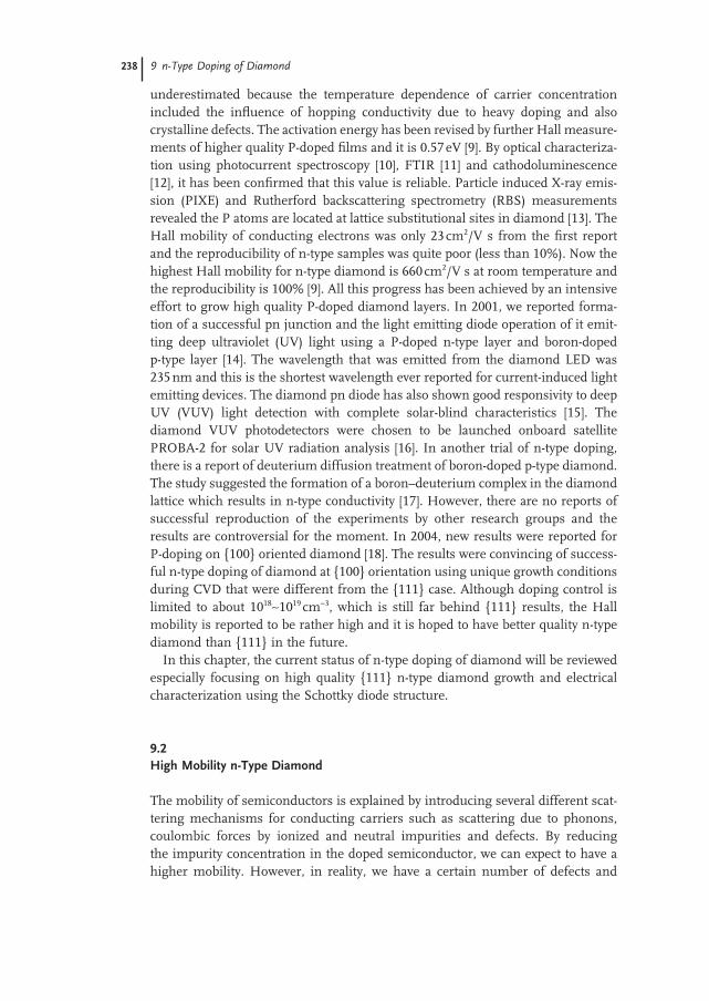
P - doped diamond fi lms with various P concentrations. The carrier concentrations are directly proportional to the P concentrations. The carrier concentration and resistivity of a P - doped fi lm with a P concentration of 9 × 10 16 cm − 3 were 5 × 10 10 cm − 3 and 2 × 10 5 Ω cm at RT, 6 × 10 16 cm − 3 and 2 Ω cm at 873 K, respectively. For a non - degenerate semiconductor, the activation energy and the compensation ratio can be calculated using the following equation as usually given in conven-tional semiconductor physics textbooks:
n n N
N N n
N
g
E
kT
A
D A
C( )exp
+− −
= −( )D , (9.1)
where n is the carrier concentration, N D and N A are the donor and acceptor con-centrations, N C is the effective density of states in the conduction band, g is the degeneracy factor for the donor, E D is the activation energy of the donor, k is the Boltzmann constant and T is the temperature. For the P - doped fi lms grown at PH 3 /CH 4 : 100 ppm, we obtained E D = 0.57 eV, N D = 8.9 × 10 16 cm − 3 , N A = 1.2 × 10 16 cm − 3 , and the compensation ratio N A / N D = 0.13. In a fi lm with a P concentra-tion of 2.3 × 10 16 cm − 3 , N A was 1.5 × 10 16 cm − 3 . With decreasing P concentration below 1 × 10 16 cm − 3 , P - doped fi lms become fully compensated and highly resistant. These results suggest that in the present study, the concentration of compensating defects that exists naturally in the 111 CVD fi lm is of the order of 10 15 cm − 3 .
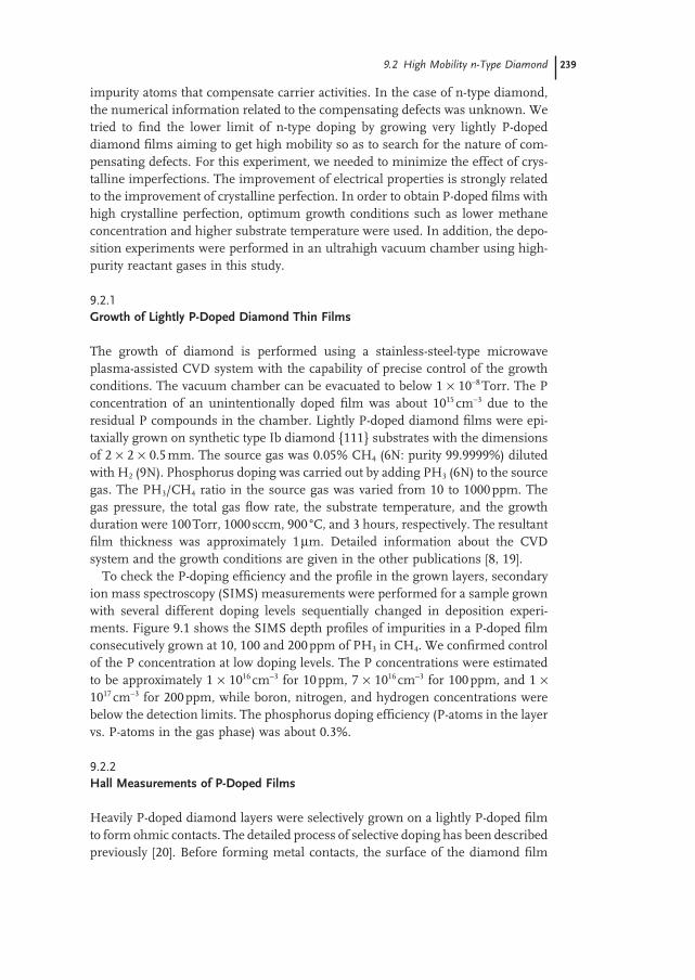
Figure 9.3 shows the Hall mobility of the P - doped fi lms as a function of tem-perature. The Hall mobility at RT increases from 180 to 660 cm 2 /V s with decreas-ing P concentrations from 3 × 10 18 to 7 × 10 16 cm − 3 . The value of 660 cm 2 /V s is the highest ever reported for n - type diamond fi lms. At P concentrations below 7 × 10 16 cm − 3 , however, no improvement in the Hall mobility has been achieved. This may be ascribed to the existence of a large amount of compensating acceptors. The Hall mobility for the P - doped fi lm with a P concentration of 7 × 10 16 cm − 3
Figure 9.3 Temperature dependence of Hall mobility for P - doped diamond fi lms with P concentrations of 7 × 10 16 , 1 × 10 18 cm − 3 and 3 × 10 18 cm − 3 .
300 400 500 600 700 800 90040
6080
100
200
400
600800
1000
7x1016 cm-3
1x1018 cm-3
3x1018 cm-3
µ ∝ T -1.4
µ ∝ T -2.6
Hal
l mob
ility
µ [c
m2 /V
s]
Temperature [K]
9.2 High Mobility n-Type Diamond 241
242 9 n-Type Doping of Diamond
decreases with increasing temperature as T − 1.4 up to 450 K. This indicates that acoustic phonon scattering dominates. At temperatures above 450 K, the Hall mobility is proportional to T − 2.6 . These two temperature dependencies are repre-sentative of the phonon scattering with a small contribution due to impurity (see the next section).
9.2.3 Calculation of the Hall Mobility Temperature Dependence
In order to quantitatively describe the temperature dependence of the Hall mobil-ity, we used the procedure described in Ref. [21] taking into account all electron scattering mechanisms relevant for diamond: intravalley acoustic phonons ( ac ), intervalley phonons ( iph ), ionized impurities ( ii ) and neutral impurities ( ni ), all within the relaxation time approximation. Six equivalent minima of the conduc-tion band are considered at 2 π / a (0.75, 0, 0) close to the X point of the Brillouin zone associated to the following effective masses for the principal directions: m || = 1.81 m 0 , m ⊥ = 0.306 m 0 [22] . The value of the deformation potential D A for the intravalley acoustic phonon scattering is treated as a fi tting parameter. Since the diamond is a multivalley semiconductor, the intervalley phonon scattering is included taking into account scattering between opposite valley (g - scattering) and non - opposite valley (f - scattering), in analogy to silicon [23] . The selection rules for phonons in inter - valley scattering processes give the LO mode for g - scattering and LA and TO for f - scattering. Geometrical considerations show that the LO phonon (g - scattering) is at the midpoint (halfway from the boundary) while LA and TO phonons (f - scattering) lie at the edge of the Brillouin zone in the ∆ direction. The energies used in the calculations are ω f = 140 meV for the f - scattering and ω g = 165 meV for the g - scattering [24] . Since these phonons have non - zero energy, the intervalley scattering mode is inelastic, and so the procedure of Farvacque was used [25] . The intervalley coupling constants ( D if and D ig ) between these phonons and the electrons are treated as adjustable parameters, but in order to limit the number of adjustable parameters they are assumed to be equal. The intravalley scattering mechanism due to optical phonons is forbidden by the selection rules, and was thus neglected. Electron scattering by phonons with a fi nite energy (inter-valley) starts at very high temperature, due to the high energy of phonon in diamond, so that these coupling constants are determined with a lower precision than in the case of acoustic phonons.
For ionized impurity scattering, the relaxation time is inversely proportional to N i = n + 2 × N A , N i being the number of ionized impurity, n the free electron density and N A the compensating centers (acceptor) density. The neutral impurity (ni) scattering was treated using an effective Rydberg of 570 meV. The relaxation time of the ni mode is inversely proportional to N n = N D − N A − n , where N n is the number of neutral impurities and N D the phosphorus (donor) density. N D , N A and n are obtained from the fi t of the Hall electron density to experimental data through the neutrality equation. Then, the total relaxation time was calculated using the Mathiessen rule and the Hall mobility is defi ned by µ τH H H*= < >r e m/ . In
this equation, the Hall factor r H is assumed to be unity, < τ > is the average value of τ as defi ned in Ref. [21] and m m m m mH* = + +⊥ ⊥( )/( / )|| ||2 2 the Hall mobility mass. In order to determine precisely the acoustic deformation potential, calcula-tions were compared with the experimental Hall mobility for several samples over a wide range of temperature (293 K to 873 K).
Figures 9.4 a and b show the theoretical contributions of various modes and the total Hall mobility. N D and N A are determined from the fi t of the electron density temperature dependence using the neutrality equation. The intrinsic diamond parameters determined from the fi t of the mobility were the acoustic deformation potential equals to 17.7 eV and the intervalley coupling constants equal to D if = D ig = 4.2 × 10 9 eV/cm [26] . The resulting acoustic deformation potential value is higher than in silicon (9.5 eV [23] ) and 4H – SiC (11.4 eV [21] ) showing more effi cient coupling between electrons and acoustic phonons in diamond. Using another set of effective masses from the literature ( m || = 1.5 m 0 , m ⊥ = 0.26 m 0 [27] ), the deter-mined acoustical deformation potential would be 21.5 eV. The D if and D ig are effective since in fact, if we want to evaluate the coupling constant of a single phonon, we must consider the number of equivalent valleys to which the electron could be scattered (4 for f - scattering and 1 for g - scattering) and the number of different phonons able to scatter the incident electron with respect to the selection rules (1 phonon LA and 1 phonon TO for f - scattering and 1 phonon LO for g - scattering). In this way, an approximate value of D i with a physical meaning can be evaluated as 9.3 × 10 8 eV/cm in good agreement with the 8 × 10 8 eV/cm deter-mined in Ref [28] .
For sample [P] SIMS = 7 × 10 16 cm − 3 (see Figure 9.4 a), intravalley acoustic scattering dominates the RT mobility, giving the maximum measured Hall mobility of 660 cm 2 /Vs. This is due to the low density of compensating centers ( N A = 8.8 × 10 15 cm − 3 ) which induces a low contribution of the ionized impurity mode to the total mobility. Above 700 K intervalley scattering limits the mobility and ionized
Figure 9.4 Experimental Hall electron mobility as a function of temperature (logarithmic scale) for P - doped diamond fi lms with P concentrations (SIMS) of (a) 7 × 10 16 and (b) 3 × 10 18 cm − 3 . The solid lines show theoretical
contribution of various modes and total mobility (tot). The different scattering mechanisms are ionized impurities (ii), neutral impurities (ni), acoustic phonons (ac), intervalley phonons (iph).
9.2 High Mobility n-Type Diamond 243
244 9 n-Type Doping of Diamond
impurity scattering is negligible. Neutral impurity scattering has no infl uence over the whole temperature range. In the case of sample [P] SIMS = 3 × 10 18 cm − 3 (see Figure 9.4 b), the intrinsic scattering modes due to the lattice are the same as in the previous sample. The differences between the mobility curves of the two samples come from the doping level which is about fourty times higher and from the compensating center density ( N A = 1.12 × 10 17 cm − 3 ) which is about twenty times higher. The higher neutral phosphorus concentration increases the effect of the ni scattering on the total mobility. In the same way, the uptake of compen-sating centers reduces the total mobility through the ii mode. Indeed, at RT the condition n << N A applies and the ii scattering time is inversely proportional to N A . At room temperature, the ni and ii scattering modes have a comparable infl u-ence to the total mobility. The infl uence of the impurity scattering (ni and ii) can be directly observed in Figure 9.4 for two different doping and compensation levels.
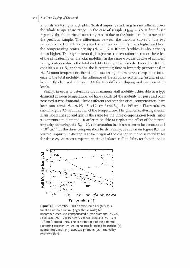
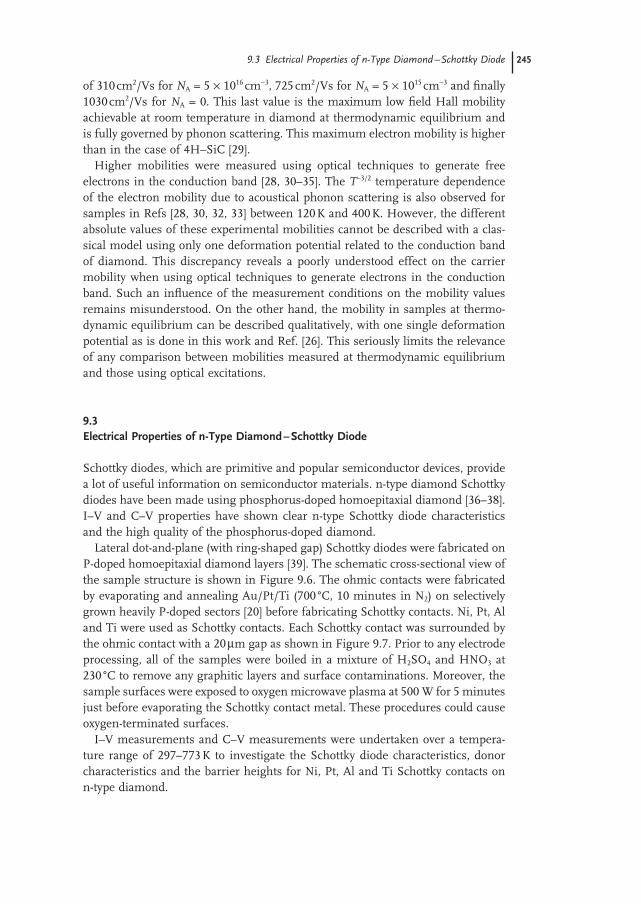
Finally, in order to determine the maximum Hall mobility achievable in n - type diamond at room temperature, we have calculated the mobility for pure and com-pensated n - type diamond. Three different acceptor densities (compensation) have been considered: N A = 0, N A = 5 × 10 15 cm − 3 and N A = 5 × 10 16 cm − 3 . The results are shown Figure 9.5 as a function of the temperature. The phonon scattering mecha-nism (solid lines ac and iph) is the same for the three compensation levels, since it is intrinsic to diamond. In order to be able to neglect the effect of the neutral impurity scattering, the N D − N A concentration has been taken to be constant at 1 × 10 15 cm − 3 for the three compensation levels. Finally, as shown on Figure 9.5 , the ionized impurity scattering is at the origin of the change in the total mobility for the three N A . At room temperature, the calculated Hall mobility reaches the value
Figure 9.5 Theoretical Hall electron mobility (tot) as a function of temperature (logarithmic scale) for uncompensated and compensated n - type diamond. N A = 0, solid lines, N A = 5 × 10 15 cm − 3 , dashed lines and N A = 5 × 10 16 cm − 3 , dotted lines. The contributions of the different scattering mechanism are represented: ionized impurities (ii), neutral impurities (ni), acoustic phonons (ac), intervalley phonons (iph).
9.3 Electrical Properties of n-Type Diamond – Schottky Diode 245
of 310 cm 2 /Vs for N A = 5 × 10 16 cm − 3 , 725 cm 2 /Vs for N A = 5 × 10 15 cm − 3 and fi nally 1030 cm 2 /Vs for N A = 0. This last value is the maximum low fi eld Hall mobility achievable at room temperature in diamond at thermodynamic equilibrium and is fully governed by phonon scattering. This maximum electron mobility is higher than in the case of 4H – SiC [29] .
Higher mobilities were measured using optical techniques to generate free electrons in the conduction band [28, 30 – 35] . The T − 3/2 temperature dependence of the electron mobility due to acoustical phonon scattering is also observed for samples in Refs [28, 30, 32, 33] between 120 K and 400 K. However, the different absolute values of these experimental mobilities cannot be described with a clas-sical model using only one deformation potential related to the conduction band of diamond. This discrepancy reveals a poorly understood effect on the carrier mobility when using optical techniques to generate electrons in the conduction band. Such an infl uence of the measurement conditions on the mobility values remains misunderstood. On the other hand, the mobility in samples at thermo-dynamic equilibrium can be described qualitatively, with one single deformation potential as is done in this work and Ref. [26] . This seriously limits the relevance of any comparison between mobilities measured at thermodynamic equilibrium and those using optical excitations.
9.3 Electrical Properties of n - Type Diamond – Schottky Diode
Schottky diodes, which are primitive and popular semiconductor devices, provide a lot of useful information on semiconductor materials. n - type diamond Schottky diodes have been made using phosphorus - doped homoepitaxial diamond [36 – 38] . I – V and C – V properties have shown clear n - type Schottky diode characteristics and the high quality of the phosphorus - doped diamond.
Lateral dot - and - plane (with ring - shaped gap) Schottky diodes were fabricated on P - doped homoepitaxial diamond layers [39] . The schematic cross - sectional view of the sample structure is shown in Figure 9.6 . The ohmic contacts were fabricated by evaporating and annealing Au/Pt/Ti (700 ° C, 10 minutes in N 2 ) on selectively grown heavily P - doped sectors [20] before fabricating Schottky contacts. Ni, Pt, Al and Ti were used as Schottky contacts. Each Schottky contact was surrounded by the ohmic contact with a 20 µ m gap as shown in Figure 9.7 . Prior to any electrode processing, all of the samples were boiled in a mixture of H 2 SO 4 and HNO 3 at 230 ° C to remove any graphitic layers and surface contaminations. Moreover, the sample surfaces were exposed to oxygen microwave plasma at 500 W for 5 minutes just before evaporating the Schottky contact metal. These procedures could cause oxygen - terminated surfaces.
I – V measurements and C – V measurements were undertaken over a tempera-ture range of 297 – 773 K to investigate the Schottky diode characteristics, donor characteristics and the barrier heights for Ni, Pt, Al and Ti Schottky contacts on n - type diamond.
246 9 n-Type Doping of Diamond
9.3.1 Schottky Diode Characteristics
Figure 9.8 shows typical I – V characteristics from 297 K to 773 K of the Ni/n - type diamond Schottky diode. The P concentration was 1.6 × 10 16 cm − 3 . We have obtained excellent Schottky junction properties even at 773 K as shown in this fi gure. The rectifi cation ratio was ∼ 10 6 at ± 10 V for 573 K, and the ideality factor had a minimum value of 1.0 at this temperature. The forward current density at 10 V was 0.2 A/cm 2 at 773 K. The reverse current gradually increased with increas-ing voltage at 573 K as show in Figure 9.9 . This relatively large reverse current cannot be explained by the conventional I – V equation of Schottky junctions.
Figure 9.10 shows typical current density (J) - V curves for Ni, Pt, Al and Ti Schottky contacts at 473 K for several P concentrations. We have obtained clear rectifying characteristics for every kind of metal contact. The rectifying character-istics deteriorated with increasing P concentration. It was diffi cult to obtain good Schottky diodes for high P concentration (3.4 × 10 19 cm − 3 ), and J – V characteristics
Figure 9.6 Schematic cross - sectional view of the Schottky diode.
Schottky contactSiO2
P-doped layer
111 Diamond substrate
Ohmic contact
Figure 9.7 Plane view of the electrode pattern of the lateral dot and plane Schottky barrier diode. (a) Whole sample area. (b) Three different areas of Schottky contacts.
9.3 Electrical Properties of n-Type Diamond – Schottky Diode 247
came closer to ohmic - like characteristics. The results suggest that the heavily P - doped layer can act as a good contact layer [20] .
9.3.2 P - Related Donor Characteristics
Typical results of the capacitance (C) and the conductance divided frequency ( G / ω , w = 2 π f ) at zero dc bias voltage are shown as a function of frequency ( f ) for sample temperatures ( T = 297 – 673 K) in Figure 9.11 a and b), respectively. The capacitance strongly depends on frequency and temperature. The observed variation in
Figure 9.8 Typical I – V curve at 297 K, 373 K, 473 K, 573 K and 773 K of the Ni/n - type diamond Schottky diode.
Figure 9.9 Reverse I – V characteristics of the sample shown in Figure 9.8 .
Figure 9.10 Typical J – V curves for Ni, Pt, Al and Ti Schottky contacts on P - doped diamond layers.
Figure 9.11 A typical result of the capacitance (C) and the conductance divided by frequency ( G / ω ) at zero bias voltage as a function of frequency ( f ) for several temperatures ( T = 297 K, 323 K, 373 K, 423 K, 523 K, 623 K and 673 K) for P - doped diamond.
9.3 Electrical Properties of n-Type Diamond – Schottky Diode 249
capacitance can be due to the high resistivity of the diamond and/or to the well - known dispersion effect, which occurs when a deep level is unable to follow the high frequency voltage modulation and unable to contribute to the net space charge in the depletion region. In most semiconducting materials, the former effect is relatively unimportant since the capacitance values were obtained from the series mode resistance of the inductance – capacitance – resistance (LCR) meter, in which the capacitance is determined independently of any series resistance. We have obtained the activation energy of 0.54 eV for this sample from the slope of the plot of ω peak / T 2 against the reciprocal temperature. Where, ω peak is the peak frequency of the G / ω determined from the results of the G / ω - f measurements. The detailed calculation procedure has been shown in a previous paper (admit-tance spectroscopy [40] ). This value is a little smaller than the P donor activation energy ( ∆ E D ∼ 0.57 eV) measured by temperature - dependent Hall effect measure-ments or optical measurements reported in the literature [9, 12, 41, 42] . It is assumed that the applied electric fi eld during C – V measurements gives rise to barrier height lowering. The observed variations in the C – f curves were considered to show the activation and deactivation of P donor. This result indicates the net donor concentration should be determined in the capacitance saturation region from the C – V measurements.
Figure 9.12 shows a typical result of the C – V measurements in such a capaci-tance saturation region (1 kHz, 373 K) for the same sample as that shown in Figure 9.11 . The 1/ C 2 – V plot had good linearity as shown in Figure 9.12 . The capacitance of the depletion region for the Schottky junction can be written using the following equation [43] ,
Figure 9.12 Typical C – V and 1/ C 2 curves at 573 K for the Ni/P - doped diamond Schottky diode. The applied frequency was 1 kHz.
250 9 n-Type Doping of Diamond
C Aq N N
V V
S D A
bi
= −−
ε ( )
( ),
2 (9.2)
where ( N D – N A ) is the net donor concentration, V bi is the built - in potential, q is the elementary charge, ε s is the permittivity of semiconductor ( ε s = ε sr ε 0 ), and A is an area of the Schottky contact. The net donor concentration ( N D – N A ) denotes the net positively charged ionized impurity concentration in the depletion region, and is given by the following equation (from the Equation 9.2 )
N Nq d C dV A
D A
S
− = −
2 11
12 2ε ( / )/
. (9.3)
It was evaluated to be 1.3 × 10 16 cm − 3 from the slope of the 1/ C 2 against voltage plot with relative dielectric constant of diamond, ε s of 5.7. Figure 9.13 shows the net donor concentration as a function of the P concentration. It was found that P electrical activity, which means the ratio of the net donor concentration to the P concentration, was near 1 for P concentrations of 1.6 × 10 16 cm − 3 to 2.7 × 10 18 cm − 3 . The ratio of the uncompensated P concentration to the total P concentration was considered to be very high. This is a result of the fact that the background acceptor concentration in the P - doped layers is quite low in comparison with the acceptor concentration or P concentration, such as ∼ 10 15 cm − 3 or less. Figure 9.14 shows the depth profi le of P and other residual impurity concentrations for a typical P - doped diamond layer. P concentration is almost constant in the P - doped epitaxial layer, and it is not detected ( < 1 × 10 15 cm − 3 ) in the diamond substrate. Hydrogen and boron, which may compensate P donors, are not detected. Although the detec-tion limit of hydrogen concentration ( ∼ 10 18 cm − 3) is comparable to the P doping
Figure 9.13 Net donor concentration as a function of phosphorus concentration in P - doped diamond.
9.3 Electrical Properties of n-Type Diamond – Schottky Diode 251
level, it is signifi cantly small for compensating P - donors [44, 45] . Moreover, this result of high uncompensated P donor concentration is consistent with the results of the Hall effect measurements [46] and/or the PIXE ( particle - induced X - ray emission ) measurements [13] .
9.3.3 Electrical Properties of Metal/ n - Type Diamond Interfaces
9.3.3.1 Schottky Barrier Height Dependence on Metal Work Function Built - in potential, V bi , can be determined by extrapolation of 1/ C 2 to 0 as shown in the following equation (from Equation 9.2 ),
V Vq N N
C Abi
S D A− = − ( )ε ( ).
21 1
2 2 (9.4)
As shown in Figure 9.12 , V bi of 3.8 eV was obtained from the extrapolation of 1/ C 2 to 0 at 573 K for the diode. This value gives the Schottky barrier height of 4.3 eV from the next equation [43] ,
φBn bi nqV qV= + (9.5)
where qV n is the energy difference between the Fermi level ( E F ) and the bottom of the conduction band ( E C ). qV n is given by
qV E EkT
q
N
nn C F
C= − = ln , (9.6)
Figure 9.14 Depth profi les of P and residual impurity (H, B, N) concentration determined by SIMS measurements.
252 9 n-Type Doping of Diamond
where N C is the density of states in the conduction band, n is the electron concentration at the temperature T , and k is the Boltzmann constant. The qV n was calculated to be about 0.5 eV at 573 K for the sample. The value of the Schottky barrier height, 4.3 eV, is considerably higher compared to those of other semicon-ductors. One of the reasons for such a large value is the small value of the electron affi nity of diamond. For an ideal Schottky contact between a metal and an n - type semiconductor in the absence of surface states, the barrier height can be equal to the energy difference between the metal work function ( φ m ) and the electron affi n-ity of the semiconductor ( χ ),
φ φ χBn m= − . (9.7)
Assuming that Ni has a work - function of φ WF = 5.15 eV [47] and the electron affi nity of (111) diamond is assumed to be χ D = 0.38 eV [48] , the Schottky barrier height should be:
φ φ χSCH WF D eV= − = 4 77. . (9.8)
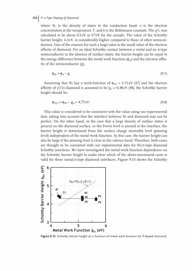
This value is considered to be consistent with the value using our experimental data, taking into account that the interface between Ni and diamond may not be perfect. On the other hand, in the case that a large density of surface states is present on the diamond surface, or the Fermi level is pinned at the interface, the barrier height is determined from the surface charge neutrality level (pinning level) independent of the metal work function. In this case, the barrier height can also be large if the pinning level is close to the valence band. Therefore, both cases are thought to be consistent with our experimental data for Ni/n - type diamond Schottky junctions. We have investigated the metal work function dependence on the Schottky barrier height to make clear which of the above - mentioned cases is valid for these metal/n - type diamond interfaces. Figure 9.15 shows the Schottky
Figure 9.15 Schottky barrier height as a function of metal work function for P - doped diamond.
9.3 Electrical Properties of n-Type Diamond – Schottky Diode 253
barrier height as a function of the metal work function. All of the Schottky diodes, shown in this fi gure, show good linear relationship between 1/ C 2 and V . The barrier height is almost constant at around 4.3 eV, independent of the metal work function. The dotted line shows that the Schottky limit, or S factor, is one. This result that the S factor is almost zero indicates that the Fermi level is strongly pinned at the metal/n - type diamond interfaces below ∼ 4.3 eV from the bottom of the conduction band as shown in Figure 9.16 . This strong pinning of the Fermi level at the metal/diamond interfaces may be related to a high density of states at approximately 1.7 eV above the valence band resulting from oxygen termination [49] .
9.3.3.2 Comparison Between n - Type and p - Type Diamond Electrical characteristics of Ni/n - type diamond interfaces were compared to those of Ni/p - type diamond interfaces for (111) oriented homoepitaxial diamond. The electrode processing and the surface treatment were the same for n - type Schottky diodes and for p - type Schottky diodes. The built - in potential for the p - type Schottky diode was found to be 1.3 V from the results of C – V measurements as shown in Figure 9.17 . The Schottky barrier height was evaluated to be 1.6 eV from Equations 9.4 and 9.5 . Thus, the sum of the Ni Schottky barrier heights of p - type and n - type diamond was 5.9 eV. This value was approximately consistent with the bandgap energy of diamond. Considering the surface Fermi level pinning for p - type Schottky junctions on (100) diamond [50] , it is possible that the surface Fermi level is pinned at the same energy level in the band gap for p - type and n - type diamond.
Figure 9.16 Schematic energy - band diagram of metal/n - type diamond under thermal equilibrium condition. Schottky barrier height as a function of metal work function for P - doped diamond.
n-type diamondMetal
Eg = 5.5eV
Fermi level pinning
Pinned
fBn~4.3eV
EV
EF
Ec
qVn
qVbi
254 9 n-Type Doping of Diamond
9.4 Summary
Lightly phosphorus doped 111 homoepitaxial diamond fi lms have been grown by microwave plasma - assisted CVD. We demonstrated the capability of phospho-rus doping control at the concentrations as low as 10 16 cm − 3 with clear signatures of n - type conductivity characterized by Hall measurements. The highest value of the Hall mobility at RT is 660 cm 2 /V s obtained for a fi lm with a phosphorus con-centration of 7 × 10 16 cm − 3 . We conclude that lightly P - doped diamond fi lms with high crystalline perfection can be successfully obtained.
The low fi eld Hall mobility was described as a function of temperature using the relevant scattering modes. The intrinsic parameters of phonons were deter-mined and the scattering mechanisms of the electron Hall mobility established. The maximum Hall mobility achievable in n - type diamond has been determined at room temperature. Evidence is provided for a discrepancy between low fi eld Hall mobility at thermodynamical equilibrium and electron mobilities deduced from optically excited experiments.
I – V and C – V measurements were carried out over a wide range of temperatures and P concentrations to investigate the electrical properties of n - type diamond Schottky barrier diodes and metal/diamond interfaces for P - doped homoepitaxial diamond. We have obtained excellent Schottky diode properties from 297 K to 773 K. The ideality factor is 1.0 at ± 10 V for 573 K and the rectifi cation ratio is ∼ 10 6 at these temperatures. The rectifying characteristics deteriorated with increasing P concentration, becoming closer to ohmic - like characteristics when the P concen-tration is very high (3.4 × 10 19 cm − 3 ). Frequency - dependent capacitance measure-ments reveal a P - related deep donor state. The donor activation energy is calculated to be 0.54 eV from conductance – frequency measurements. P electrical activity, which means the ratio of the net donor concentration to the P concentrations
Figure 9.17 Typical C – V and 1/C 2 − V curves of Ni/B - doped diamond Schottky diode (300 K, 3 kHz).
References 255
detected by SIMS, is nearly one even at low P concentration (1.6 × 10 16 cm − 3 ). The Schottky barrier height is ∼ 4.3 eV independent of the metal work function. The result suggests that the Fermi level is strongly pinned at the metal/diamond inter-faces ∼ 4.3 eV below the bottom of the conduction band. A comparison with other metals shows no barrier variation, so that Fermi level pinning due to surface defect state is detected. The fact that the sum of Schottky barrier heights of the same metal on p - type and n - type diamond is close to the bandgap energy indicates that oxygen termination may result in a high density of surface states at the same energy level from the valence band maximum on p - type and n - type (111) diamond surface.
References
1 Kajihara , S.A. , Antonelli , A. and Bernholc , J. ( 1993 ) Physica B , 185 ( 1 – 4 ), 144 – 9 .
2 Alexenko , A.E. and Spitsyn , B.V. ( 1992 ) Diamond and Related Materials , 1 , 705 – 9 .
3 Kamo , M. , Yurimoto , H. , Ando , T. and Sato , Y. ( 1991 ) Proceeding of the 2nd
International Conference on New Diamond
Science and Technology (eds S.R. Messier , J.T. Glass , J.E. Butler and R. Roy ), Materials Research Society , Pittsburgh , p. 637 .
4 Okano , K. , Kiyota , H. , Iwasaki , T. , Nakamura , Y. , Akiba , Y. , Kurosu , T. , Iida , M. and Nakamura , T. ( 1990 ) Applied
Physics A , 51 , 344 – 6 . 5 Koizumi , S. , Ozaki , H. , Kamo , M. , Sato ,
Y. and Inuzuka , T. ( 1997 ) Applied Physics
Letters , 71 , 1064 – 7 . 6 Koizumi , S. , Kamo , M. , Sato , Y. , Mita , S. ,
Sawabe , A. , Reznik , A. , Uzan - Saguy , C. and Kalish , R. ( 1998 ) Diamond and
Related Materials , 7 ( 2 – 5 ), 540 – 4 . 7 Koizumi , S. ( 1999 ) physica status solidi
(a) , 172 , 71 – 8 . 8 Koizumi , S. ( 2003 ) Semiconductors and
Semimetals , 76 , 239 – 59 . 9 Katagiri , M. , Isoya , J. , Koizumi , S. and
Kanda , H. ( 2004 ) Applied Physics Letters , 85 ( 26 ), 6365 – 7 .
10 Nesl á dek , M. , Meykens , K. , Haenen , K. , Knuyt , G. , Stals , L.M. , Teraji , T. and Koizumi , S. ( 1999 ) Physical Review B , 59 , 14852 .
11 Gheeraert , E. , Koizumi , S. , Teraji , T. and Kanda , H. ( 2000 ) Solid State
Communications , 113 , 577 .
12 Sternschulte , H. , Thonke , K. , Sauer , R. and Koizumi , S. ( 1999 ) Physical Review B , 59 , 12924 .
13 Hasegawa , M. , Teraji , T. and Koizumi , S. ( 2001 ) Applied Physics Letters , 79 , 3068 .
14 Koizumi , S. , Watanabe , K. , Hasegawa , M. and Kanda , H. ( 2001 ) Science , 292 , 1899 .
15 BenMoussa , A. , Sch ü hle , U. , Haenen , K. , Nesl á dek , M. and Koizumi , S. and Hochedez , J. - F. ( 2004 ) physica status solidi
(a) , 201 ( 11 ), 2536 – 41 . 16 BenMoussa , A , Sch ü hle , U. , Scholze , F. ,
Kroth , U. , Haenen , K. , Saito , T. , Campos , J. , Koizumi , S. , Laubis , C. , Richter , M. , Mortet , V. , Theissen , A. and Hochedez , J.F. ( 2006 ) Measurement Science and
Technology , 17 , 913 – 17 . 17 Teukam , Z. , Chevallier , J. , Saguy , C. ,
Kalish , R. , Ballutaud , D. , Barbe , M. , Jomard , F. , Tromson - Carli , A. , Cytermann , C. , Butler , J.E. , Bernard , M. , Baron , C. and Deneuville , A. ( 2003 ) Nature Materials , 2 ( 7 ), 482 – 6 .
18 Kato , H. , Yamasaki , S. and Okushi , H. ( 2005 ) Applied Physics Letters , 86 ( 22 ), 222111 .
19 Koizumi , S. , Teraji , T. and Kanda , H. ( 2000 ) Diamond and Related Materials , 9 , 935 .
20 Teraji , T. , Katagiri , M. , Koizumi , S. , Ito , T. and Kanda , H. ( 2003 ) Japanese Journal of
Applied Physics , 42 , L882. 21 Pernot , J. , Zawadzki , W. , Contreras , S. ,
Robert , J.L. , Neyret , E. and Di Cioccio , L. ( 2001 ) Journal of Applied Physics , 90 , 1869 .
256 9 n-Type Doping of Diamond
22 Gheeraert , E. , Koizumi , S. , Teraji , T. and Kanda , H. ( 2001 ) Diamond and Related
Materials , 10 , 444 . 23 Lundstrom , M. ( 2000 ) Fundamentals of
Carrier Transport , Cambridge University Press , Cambridge .
24 Solin , S.A. and Ramdas , A.K. ( 1970 ) Physical Review B , 1 , 1687 .
34 Pan , L.S. , Kania , D.R. , Pianetta , P. , Ager , J.W. , III , Lanstrass , M.I. and Han , S. ( 1993 ) Journal of Applied Physics , 73 , 2888 .
35 Isberg , J. , Hammersberg , J. , Johansson , E. , Wikstr ö m , T. , Twitchen , D.J. , Whitehead , A.J. , Coe , S.E. and Scarsbrook , G.A. ( 2002 ) Science , 297 , 1670 .
36 Suzuki , M. , Yoshida , H. , Sakuma , N. , Ono , T. , Sakai , T. and Koizumi , S. ( 2004 ) Applied Physics Letters , 84 , 2349 .
37 Suzuki , M. , Koizumi , S. , Katagiri , M. , Yoshida , H. , Sakuma , N. , Ono , T. and Sakai , T. ( 2004 ) Diamond and Related
Materials , 13 , 2037 . 38 Suzuki , M. , Koizumi , S. , Katagiri , M. ,
Ono , T. , Sakuma , N. , Yoshida , H. and Sakai , T. ( 2006 ) physica status solidi (a) , 203 , 3128 .
39 Suzuki , M. , Yoshida , H. , Sakuma , N. , Ono , T. , Sakai , T. , Ogura , M. , Okushi , H. and Koizumi , S. ( 2004 ) Diamond and
Related Materials , 13 , 198 . 40 Koide , Y. , Koizumi , S. , Kanda , H. , Suzuki ,
M. , Yoshida , H. , Sakuma , N. , Ono , T. and Sakai , T. ( 2005 ) Applied Physics Letters , 86 , 232105 .
41 Nesladek , M. ( 2005 ) Semiconductor Science
and Technology , 20 , 19 . 42 Gheeraert , E. , Koizumi , S. , Teraji , T. ,
Kanda , H. and Nesladek , M. ( 2000 ) Diamond and Related Materials , 9 , 948 .
43 Rhoderik , E.H. and Williams , R.H. ( 1988 ) Metal – Semiconductor Contacts , 2nd edn, Oxford University Press , New York .
44 Chevallier , J. , Jormard , F. , Teukam , Z. , Koizumi , S. , Kanda , H. , Sato , Y. , Deneuville , A. and Bernard , M. ( 2002 ) Diamond and Related Materials , 11 , 1566 .
45 Ando , J.T. , Haneda , H. , Akaishi , M. , Sato , Y. and Kamo , M. ( 1996 ) Diamond and
Related Materials , 5 , 34 . 46 Nesladek , M. , Haenen , K. and Vanecek , M.
( 2003 ) Semiconductors and Semimetals
76 – Thin Film Diamond I (eds C.E. Nebel and J. Ristein ), Elsevier Academic Press , Amsterdam , p. 325 .
47 Michaelson , J.H.B. ( 1977 ) Journal of
Applied Physics , 48 , 4729 . 48 Ristein , J. , Maiyer , F. , Riedel , M. , Cui , J.B.
and Ley , L. ( 2000 ) physica status solidi (a) , 181 , 65 .
49 Daniesenko , A. , Aleksov , A. and Kohn , E. ( 2001 ) Diamond and Related Materials , 10 , 667 .
50 Takeuchi , D. , Yamanaka , S. , Watanabe , H. and Okushi , H. ( 2001 ) physica status solidi