PHYSICS LAB MANUAL B.Tech 1 st year List of Subject related Experiments: 1. To study the reverse characteristics of Zener diode and voltage regulation using Zener Diode. 2.To study the forward and reverse characteristics of P-N junction diode. 3. To study Hall effect in semiconductors and measure the Hall coefficient. 4. To find frequency of AC mains using sonometer. 5. To verify the inverse square law with the help of a photovoltaic cell. 6. To study the characteristics of Solar cell and find out the fill factor 7. To design and study Active and Passive filters. 8. To find impedance and Q factor using LCR circuit. 9. To study resonance phenomena in LCR circuit. 10. To measure e/m of electron using helical method. EXPERIMENT 1: Observation of characteristics of Zener diode Aim of experiment To study the reverse characteristics of Zener diode and voltage regulation using Zener Diode Apparatus required a)A Zener diode b)A DC voltage supplier c)Bread board
Transcript
PHYSICS LAB MANUAL
B.Tech 1st year
List of Subject related Experiments:
1. To study the reverse characteristics of Zener diode and voltage regulation using Zener Diode.
2.To study the forward and reverse characteristics of P-N junction diode.
3. To study Hall effect in semiconductors and measure the Hall coefficient.
4. To find frequency of AC mains using sonometer.
5. To verify the inverse square law with the help of a photovoltaic cell.
6. To study the characteristics of Solar cell and find out the fill factor
7. To design and study Active and Passive filters.
8. To find impedance and Q factor using LCR circuit.
9. To study resonance phenomena in LCR circuit.
10. To measure e/m of electron using helical method.
EXPERIMENT 1: Observation of characteristics of Zener diode Aim of experiment To study the reverse characteristics of Zener diode and voltage regulation using Zener Diode
Apparatus required a)A Zener diode b)A DC voltage supplier c)Bread board
d)2 multimeter for measuring current and voltage e)Connecting wires
Theory of experiment A Zener Diode is constructed for operation in the reverse breakdown region. The relation between I-V is almost linear in this case Vz = Vz0 +Izrz , where rz is the dynamic resistance of the zener at the operating point.Vz0 is the voltage at which the straight-line approximation of the I-V characteristic intersects the horizontal axis. After reaching a certain voltage, called the breakdown voltage, the current increases widely even for a small change in voltage. However, there is no appreciable change in voltage. So, when we plot the graph, we should get a curve very near to x-axis and almost parallel to it for quite sometime. After the Zener potential Vz there will be a sudden change and the graph will become exponential.
Procedure We first construct the circuit as shown in the figure with the 100 resistance and a variable DC input voltage. Now, we start increasing the voltage till there is some reading in the multimeter for current. Then, we note that reading. Now, we start increasing the input voltage and take the corressponding current readings. We get a set of values and construct a V vs I graph. This graph gives us the I-V characteristics. The slope of the curve at any point gives the dynamic resistance at that voltage.
Zener as voltage regulator: Procedure : 1. Connect + 12V dc power supply at their indicated position from external source 2. Connect one voltmeter between test point 1 and ground to measure input voltage Vin. 3. Connect ohmmeter between test point 4 and ground and set the value of load resistance RL at a fixed value of 1 K. 4. Connect a 2mm patch cord between test point 2 and 3. 5. Connect voltmeter between test point 4 and ground to measure output voltage Vout. 6. Switch ON the power supply.
7. Vary the potentiometer P1 to some fixed value of input voltage Vin = (6V, 7V……) and measure the corresponding value of output voltage Vout. 8. Repeat the above step and note the results in an observation Observation table:
Sr.no. Input voltage Vin Output voltage Vout (volt)
1
2
3
4
5
6
7
8 Circuit diagram and graph:
Claculations and observations Measurement of V and I in reverse bias
Result
breakdown potential, also called the zener potential i.e Vz _ V .
Discussions The precautions are quite similar to that taken in a normal diode i.e •Excessive flow of current may damage the diode •Current for sufficiently long time may change the characteristics •Zener diodes are used in voltage regulation in circuits because even when, a large current flows through, their voltage does not change appreciably.
EXPERIMENT-2
Aim : To study the V-I characteristics of a pn diode.
. Apparatus required: A variable voltage supply, semiconductor diode, ammeter,
voltmeter,connecting wire.
. Theory: A pn junction is formed by the diffusion of p type impurities at elevated
temperatures
into the n type silicon substrate for the fabrication of silicon pn diode. In pn diode the electrons
from
n-side are diffused into p-side and holes from p-side are diffused into n-side. As a result, a
region,
which is devoid of free charges, is formed near the metallurgical junction of both sides. This is
known as depletion layer. When a positive terminal of battery is connected to p-type and
negative
terminal is connected to n-type, (as shown in Fig.1), the diode is said to be forward biased. In
this
case hole from p-side tends to cross the junction from p to n and electrons from n side tend to
cross
the junction from n to p. When a positive terminal of battery is connected to n-type and negative
terminal is connected to p-type, (as shown in Fig.2), the diode is said to be reverse biased. In this
case
holes and electrons move in opposite directions unlike forward biased case.
Circuit Diagram:
:
3. Procedure:
I. Forward Characteristics (i). Make connection as in Fig.1. (ii). Vary the voltage in small steps and measure the
corresponding currents. (iii). Plot a graph between diode voltage and diode forward current.
II. Reverse Characteristics (i). Make connection as in Fig.2. (ii). Vary the voltage in small steps and measure the
corresponding currents. (iii). Plot a graph between diode voltage and diode reverse current.
4.Observations: Table for V-I characteristics of the diode
Least count of voltmeter... ..(volts)
Least count of ammeter.....(mA)
FORWARD BISE TABLE:
SR.NO VOLATGE(VOLT) CURRENT(mA)
1
2
3
4
5
6
7
8
9
10
REVERSE BISE TABLE:
Least count of volmeter...(volts)
Least count of ammeter... (μA)
SR.NO. VOLTAGE(VOLT) CURRENT(μA)
1
2
3
4
5
6
7
8
9
10
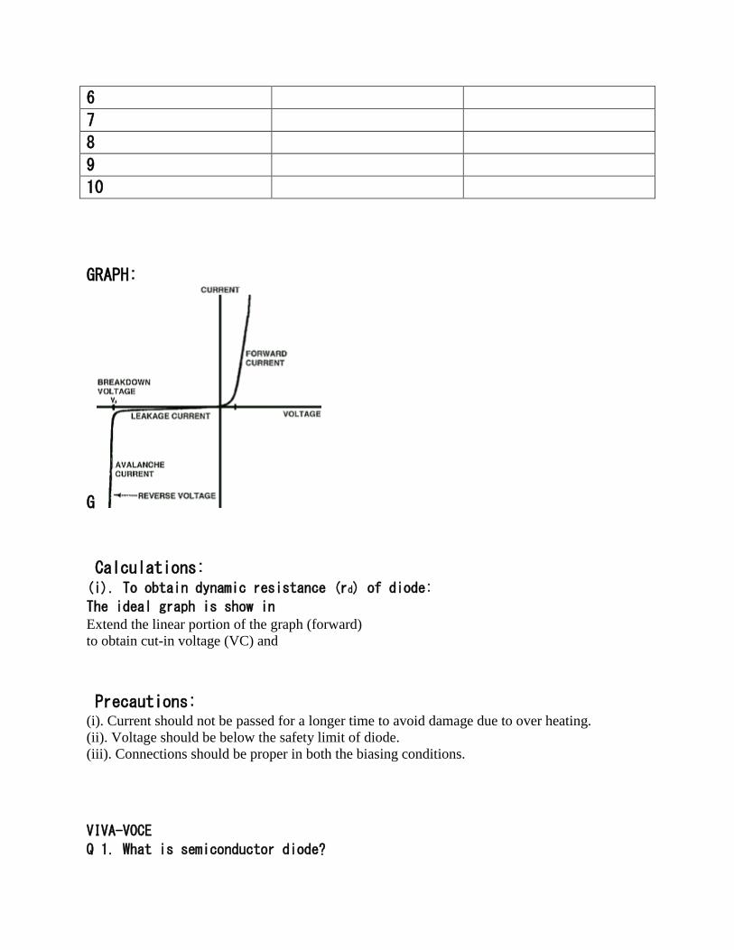
GRAPH:
G
Calculations: (i). To obtain dynamic resistance (rd) of diode:
The ideal graph is show in Extend the linear portion of the graph (forward)
to obtain cut-in voltage (VC) and
Precautions: (i). Current should not be passed for a longer time to avoid damage due to over heating.
(ii). Voltage should be below the safety limit of diode.
(iii). Connections should be proper in both the biasing conditions.
VIVA-VOCE
Q 1. What is semiconductor diode?
Ans. A p-n junction is called semiconductor diode.
Q 2. Define depletion layer?
Ans. The region having uncompensated acceptor and donor ions is called depletion layer.
Q 3. What do you mean by forward bias and reversed bias?
Ans. When p-type semiconductor is connected to the positive terminal and n-type
semiconductor
connected to negative terminal of voltage source, so that zero resistance is offered to the flow of
current, is called forward bias. When p-type semiconductor is connected to the negative terminal
and
n-type semiconductor connected to positive terminal of the voltage source, so that zero current
flows
in this condition, is called reverse bias.
Q 4. Define knee voltage?
Ans. The forward voltage at which current through the junction starts increasng rapidly.
Q 5. Define break down voltage?
Ans. The reverse voltage at which p-n junction breaks down which sudden rise in reverse
current
EXPERIMENT NO -3
AIM: To study Hall effect in semiconductors and measure the Hall coefficient
Introduction -The conductivity measurements cannot reveal whether one or types of carriers are
present; nor distinguish between them. However, this information can be obtained from Hall Effect
measurements, which are basic tools for the determination of mobilities. The effect was discovered by
E.H. Hall in 1879.
Theory -As you are undoubtedly aware, a static magnetic field has no effect on charges unless they are
in motion. When the charges flow, a magnetic field directed perpendicular to the direction of flow
produces a mutually perpendicular force on the charges. When this happens, electrons and holes will be
separated by opposite forces. They will in turn produce an electric field (E h ) which depends on the
cross product of the magnetic intensity, H, and the current density, J . The situation is demonstrated in
Fig. 1. E h = R J x H (1) Where R is called the Hall coefficient. Now, let us consider a bar of semiconductor,
having dimension, x, y and z. Let J is directed along X and H along Z then E h will be along Y, as in Fig. 2.
Then we could write I H V .z = J H V /y = R h h (2) Where Vh is the Hall voltage appearing between the
two surfaces perpendicular to y and I = J yz In general, the Hall voltage is not a linear function of
magnetic field applied, i.e. the Hall coefficient is not generally a constant, but a function of the applied
magnetic field. Consequently, interpretation of the Hall Voltage is not usually a simple matter. However,
it is easy to calculate this (Hall) voltage if it is assumed that all carriers have the same drift velocity. We
will do this in two steps (a) by assuming that carriers of only one type are present, and (b) by assuming
that carriers of both types are present.
(a) One type of Carrier-
Metals and degenerate (doped) semiconductors are the examples of this type where one carrier
dominates. The magnetic force on the carriers is E e (v H) m = × and is compensated by the Hall field F =
e E h h , where v is the drift velocity of the carriers. Assuming the direction of various vectors as before ×
E = H v h From simple reasoning, the current density J is the charge q multiplied by the number of
carriers traversing unit area in unit time, which is equivalent to the carrier density multiplied by the drift
velocity i.e. J = q n v By putting these values in equation (2) n q 1 = n v q H v.H = H J E = R h 3) From this
equation, it is clear that the sign of Hall coefficient depend upon the sign of the q. This means, in a p-
type specimen the R would be positive, while in ntype it would be negative. Also for a fixed magnetic
field and input current, the Hall voltage is proportional to 1/n or its resistivity. When one carrier
dominates, the conductivity of the material is ς = nqµ. where µ is the mobility of the charge carriers.
Thus µ = Rς (4) Equation (4) provides an experimental measurement of mobility; R is expressed in cm3
coulomb-1 thus µ is expressed in units, of cm2. volt-1 sec-1.
(b) Two type of Carriers- Intrinsic and lightly doped semiconductors are the examples of this type. In
such cases, the quantitative interpretation of Hall coefficient is more difficult since both type of carriers
contribute to the Hall field. It is also clear that for the same electric field, the Hall voltage of p-carriers
will be opposite sign from the n-carriers. As a result, both mobilities enter into any calculation of Hall
coefficient and a weighted average is the result* i.e. ( )2 h e 2 e 2 h 2 p n p n = R µ + µ µ − µ (5) Where
µh and µn are the mobilities of holes and electrons; p and n are the carrier densities of holes and
electrons. Eq. (5) correctly reduces to equation (3) when only one type of carrier is present**.
~~~~~~~~~~~~~~~~~~~~~~~~~~~~~~~~~~~~~~~~~~~~~~~~~~~~~~~~~~~~~~~~~~ * From Experiments in
Modern Physics by Adrian C.Melissions (Academic Press) p. 86. ** Both Eq. (3) and Eq. (5) have been
derived on the assumption that all carriers have same velocity; this is not true, but the exact calculation
modifies the results obtained here by a factor of only 3π /8. Since the mobilities µh and µn are not
constants but function of temperature (T) the Hall coefficient given by Eq. (5), is also a function of T and
it may become zero, even change sign. In general µn > µh so that inversion may happen only if p > n;
thus 'Hall coefficient inversion' is characteristic only of p-type semiconductors. At the point of zero Hall
coefficient, it is possible to determine the ratio of mobilities and their relative concentration. Thus we
see that the Hall coefficient, in conjunction with resistivity measurements, can provide information on
carrier densities, mobilities, impurity concentration and other values. It must be noted, however, that
mobilities obtained from Hall Effect measurements µ = Rς do not always agree with directly measured
values. The reason being that carriers are distributed in energy, and those with higher velocities will be
deviated to a greater extent for a given field. As µ we know varies with carrier velocity.
EXPERIMENTAL TECHNIQUE-
(a) Experimental Consideration Relevant to all measurements on Semiconductors -
1-. In single crystal material the resistivity may vary smoothly from point to point. In fact this is generally
the case. The question is the amount of this variation rather than its presence. Often however, It is
conventionally stated that it is constant within some percentage and when the variation does in fact fall
within this tolerance, it is ignored.
2. High resistance or rectification action appears fairly often in electrical contacts to semiconductors and
in fact is one of the major problem.
3. Soldered probe contacts, though very much desirable may disturb the current flow (shorting out part
of the sample). Soldering directly to the body of the sample can affect the sample properties due to heat
and by contamination unless care is taken. These problems can be avoided by using pressure contacts as
in the present set-up. The principle draw back of this type of contacts is that they may be noisy. This
problem can, however, be managed by keeping the contacts clean and firm.
4. The current through the sample should not be large enough to cause heating. A further precaution is
necessary to prevent 'injecting effect' from affecting the measurement. Even good contacts to
germanium for example, may have this effect. This can be minimized by keeping the voltage drop at the
contacts low. If the surface near the www.sestechno.com contacts is rough and the electric flow in the
crystal is low, these injected carriers will recombine before reaching the measuring probes. Since Hall
coefficient is independent of current, it is possible to determine whether or not any of these effects are
interfering by measuring the Hall coefficient at different values of current.
(b) Experimental Consideration with the Measurements of Hall Coefficient.- 1. The voltage appearing
between the Hall Probes is not generally, the Hall voltage alone. There are other galvanomagnetic and
thermomagnetic effects (Nernst effect, Rhighleduc effect and Ettingshausen effect) which can produce
voltages between the Hall Probes. In addition, IR drop due to probe misalignment (zero magnetic field
potential) and thermoelectric voltage due to transverse thermal gradient may be present. All these
except, the Ettingshausen effect are eliminated by the method of averaging four readings. The
Ettingshausen effect is negligible in materials in which a high thermal conductivity is primarily due to
lattice conductivity or in which the thermoelectric power is small. When the voltage between the Hall
Probes is measured for both directions of current, only the Hall voltage and IR drop reverse. Therefore,
the average of these readings eliminates the influence of the other effects. Further, when Hall voltage is
measured for both the directions of the magnetic field, the IR drop does not reverse and may therefore
be eliminated.
2. The Hall Probe must be rotated in the field until the position of maximum voltage is reached. This is
the position when direction of current in the probe and magnetic field would be perpendicular to each
other.
3. The resistance of the sample changes when the magnetic field is turned on. This phenomena called
magneto-resistance is due to the fact that the drift velocity of all carriers is not the same, with magnetic
field on, the Hall voltage compensates exactly the Lorentz force for carriers with average velocity.
Slower carriers will be over compensated and faster ones under compensated, resulting in trajectories
that are not along the applied external field. This results in effective decrease of the mean free path and
hence an increase in resistivity. Therefore, while taking readings with a varying magnetic field at a
particular current value, it is necessary that current value should be adjusted, every time. The
www.sestechno.com problem can be eliminated by using a constant current power supply, which would
keep the current constant irrespective of the resistance of the sample.
4. In general, the resistance of the sample is very high and the Hall Voltages are very low. This means
that practically there is hardly any current - not more than few micro amperes. Therefore, the Hall
Voltage should only be measured with a high input impedance (≅1M) devices such as electrometer,
electronic millivoltmeters or good potentiometers preferably with lamp and scale arrangements.
5. Although the dimensions of the crystal do not appear in the formula except the thickness, but the
theory assumes that all the carriers are moving only lengthwise. Practically it has been found that a
closer to ideal situation may be obtained if the length may be taken three times the width of the crystal.
BRIEF DESCRIPTION OF THE APPARATUS-
1. (a) Hall Probe (Ge Crystal) (b) Hall Probe (InAs) 2. Hall Effect Set-up (Digital),DHE-21 3. Electromagnet,
Model EMU-75 or EMU-50V 4. Constant Current Power Supply, DPS-175 or DPS-50 5. Digital
Gaussmeter, DGM-102
PROCEDURE-
1. Connect the widthwise contacts of the Hall Probe to the terminals marked 'Voltage' and lengthwise
contacts to terminals marked 'Current'.
2. Switch 'ON' the Hall Effect set-up and adjustment current (say few mA).
3. Switch over the display to voltage side. There may be some voltage reading even outside the
magnetic field. This is due to imperfect alignment of the four contacts of the Hall Probe and is generally
known as the 'Zero field Potential'. In case its value is comparable to the Hall Voltage it should be
adjusted to a minimum possible (for Hall Probe (Ge) only). In all cases, this error should be subtracted
from the Hall Voltage reading.
4. Now place the probe in the magnetic field as shown in fig. 3 and switch on the electromagnet power
supply and adjust the current to any desired value. Rotate the Hall probe till it become perpendicular to
magnetic field. Hall voltage will be maximum in this adjustment.
5. Measure Hall voltage for both the directions of the current and magnetic field (i.e. four observations
for a particular value of current and magnetic field).
6. Measure the Hall voltage as a function of current keeping the magnetic field constant. Plot a graph.
7. Measure the Hall voltage as a function of magnetic field keeping a suitable value of current as
constant. Plot graph.
8. Measure the magnetic field by the Gaussmeter.
CALCULATIONS-
(a) From the graph Hall voltage Vs. magnetic field calculate Hall coefficient.
(b) Determine the type of majority charge carriers, i.e. whether the crystal is n type or p type.
(c) Calculate charge carrier density from the relation Rq 1 n = nq 1 R = ⇒
(d) Calculate carrier mobility, using, the formula µn (or µp ) = Rς using the specified value of resistivity
(1/ς) given by the supplier or obtained by some other method (Four Probe Method
Questions-
1. What is Hall Effect?
2. What are n-type and p-type semiconductors?
3. What is the effect of temperature on Hall coefficient of a lightly doped semiconductor?
4. Do the holes actually move ?
5. Why the resistance of the sample increases with the increase of magnetic field?
6. Why a high input impedance device is generally needed to measure the Hall voltage?
7. Why the Hall voltage should be measured for both the directions of current as well as of magnetic
field?
EXPERIMENT NO-4
Aim: To determine the frequency of AC mains using a sonometer.
Apparatus: Sonometer with brass wire, a horse shoe magnet, a step down transformer, hanger with
weight and a screw gauge, connecting wire etc.
Formula: 𝑓 = 1/ 2Ѓ𝑇/ 𝑚 where f is the frequency of the mains A.C 𝑙 is the length of the wire vibrating in
resonance with A.C oscillations, m is the mass of wire per unit length, T ( tension in the wire)=Mg , here
𝑀 is the mass hung on the hanger.
Figure:
A sonometer is an apparatus used to study the transverse vibrations of stretched strings. It is in the form
of a hollow wooden rectangular box. On the wooden rectangular box there are two bridges and a pulley
at one end. A wire string is attached to one end of the wooden box, run over the bridges and pulley and
carries a weight hanger at the free end as shown in figure below. A sonometer is used to determine the
frequency of alternating current. A step down transformer is used for the determination of frequency of
A.C. because the voltage of the A.C. mains is 220V, which is dangerous. The step down transformer
reduces this voltage to 6 voltsThe string wire of the sonometer is a non-magnetic metallic wire like brass
or copper. A horse shoe magnet is placed at the middle of the sonometer wire so that the magnetic field
is applied perpendicular to the sonometer wire in a horizontal plane. When an alternating current of
definite frequency passes through the wire there will be interaction between the magnetic field and the
current carrying conductor. So a force will act on the conductor in a direction perpendicular to both the
field and the direction of current. When A.C. is passing through the conductor, since the current
direction reverses periodically, the direction of force also reverse periodically and hence, the conductor
vibrates. Since the current flowing is alternating, the wire vibrates with a frequency equal to the
frequency of A. C. By adjusting the length of the vibrating wire segment, this frequency can be made
equal to the natural frequency of the wire segment. Then the resonance takes place and the wire
vibrates with maximum amplitude. At this stage, the length of the wire segment is called the resonating
length and it increases with increase in the mass of the suspended weights. When the length ‘l’ of the
sonometer wire vibrates with maximum amplitude, the frequency of the applied A.C. is equal to the
natural frequency of the wire. 𝒇 = 𝟏/ 𝟐𝑻 𝒎𝒎
Procedure:
1. Place the sonometer on the table.
2. Attach a weight hanger at the free end of the string which passes over the pulley.
3. Stretch the wire by loading a suitable maximum mass on the weight hanger.
4. The sonometer wire is connected to the secondary of the step down transformer.
5. The horse shoe magnet is mounted at the middle of sonometer bed so as to produce a magnetic field
perpendicular to the wire.
6. The opposite poles of the magnet must face each other.
7. The bridges are placed on either side of the magnet at equal distance from the magnet and are close
to each other.
8. A light paper rider is placed on the wire between the bridges of the sonometer.
9. The A.C. supply is switched on.
10. The wire begins to vibrate.
11. The length of the wire between the two bridges is adjusted till the wire vibrates with maximum
amplitude. At this stage, the paper rider placed on the wire is thrown off, which shows the condition of
resonance.
12. -The length of the wire between the two bridges is measured. This is called the resonating length l.
13. Repeat the experiment for different loads.
14. The linear density of the wire, m, can be calculated using the relation, m = πr2 ρ, where r is the
radius of the wire which can be measured using the screw gauge.
15. By knowing the linear density, m, of the wire, the frequency of A.C. mains supply is calculated using
the formula
Observations:
Least count of screw gauge (Pitch/Total no. of div.) =….……….. metre Radius of wire(r) = ……….
………….metre. Density of the material of the wire (𝜌 ) =………kg/m3
TABLE:
SR.NO MASS HANG ON WIRE
TENSION T=Mg
LENGTH L1
LENGTH L2
L=L2-L1
1
2
3
4
5
Calculations:
Mass per unit length (m) = 𝜋𝑟2𝜌 = ………..kg/m.
Frequency of A.C. mains = 𝑓 = 1 /2ЃT/m
Mean frequency of A.C. (𝑓) =…………………Hz.
Result:
Observed (Mean) value of frequency of A.C. (𝑓) =…………………Hz.
Standard value of frequency of A.C. Mains = 50Hz.
Percentage Error: Standard Value – Observed Value Standard value 𝑥 100 = …………%
Precaution & Source of Error: 1. There should be no kinks in the sonometer wire.
2. Pulley should be frictionless.
3. Horse shoe magnet should be placed in the middle.
4. Mass of the hanger should be included in T.
5. The distance between the two knives edges should be altered very slowly otherwise resonance point
would be missed.
6. The diameter should be determined at various point
EXPERIMENT NO-5
EXPERIMENT: To verify inverse square law of radiations using a Photo-electric cell.
APPARATUS:
Photo cell (Selenium) mounted in the metal box with connections brought out at terminals, Lamp
holder with 60W bulb, Two moving coil analog meters (1000µA & 500mV) mounted on the front panel
and connections brought out at terminals, Two single point and two multi points patch cords.
THEORY: A device used to convert light energy into electrical energy is called Photo Electric Cell.
Photocell is based on the phenomenon of Photoelectric effect. Photo cell are of three types.
1. Photo-Emissive Cell.
2. Photo-Voltaic Cell.
3. Photo-Conductive Cell.
Photo-Emissive Cell: There are two types of photo-emissive cells; Vacuum type or gas filled type cells.
Generally, it consists of two electrodes i.e. cathode (K) and anode (A). The cathode is in the form of
semi-cylindrical plate coated with photo-sensitive material like sodium potassium or cesium i.e. alkali
metals. To have large current, it is usually coated with antimony cesium alloy or combination of bismuth,
silver, oxygen and cesium. The anode (A) is in the form of a straight wire made of nickel or platinum. The
anode (A) faces the cathode (K). These electrodes are sealed in an evacuated glass or quartz bulb
according to weather it is to be used with visible or ultra-violet light. As the current due to vacuum is
small, so to increase the current, the bulb of the cells is filled with an inert gas like helium, neon, argon
etc. at pressure of 1mm of mercury. Fig. 1. Schematic and working of photo emissive cell 2 When photo-
electrons flow from cathode to anode, they ionize the gas filled and hence the current gets modified.
The main drawback of this type of cell (i.e., gas filled cell) is that the photo-electric current does not vary
linearly with the intensity of the light. Since there is no time lag between the incident light and the flow
of electrons and hence current, therefore such a cell is used in television, photometry, fire alarm etc.
Photo-Voltaic Cell: Photo-Voltaic Cell is based on the principle of inner photo electric cell. This is called
true cell because it generates e.m.f. without the application of any external potential difference but by
only the light incident on it. It consists of a semi conductor layer formed on the surface of the metal
plate by either heat treatment or cathode sputting. A film of semi-transparent metal is coated over the
semi-conductor. This film maintains the electrical contact with the semiconductor and simultaneously
allows the incident light to fall on the semi-conductor. When light is incident on the semi-conductor,
electrons are emitted which flow in a direction opposite to the light rays. If the circuit is completed
between the surface transparent film and metal base through a low resistance galvanometer (G), the
current can be measured. If the resistance of the circuit is very small, the current is proportional to the
intensity of incident light. The main advantage of this cell is that it requires no external voltage for its
operation. This type of cell is widely used in photographic exposure meters, photometers and
illumination meters etc. Fig. 2 Schematic and working of photovoltaic cell (Solar cell)
3 Photo-Conductive Cell: Photo-Conductive Cell is also based on the principle of inner photoelectric
effect. It consists of a thin film of semi-conductor like Selenium or Thallium sulphide placed below a thin
film of semitransparent metal. The combination is place over the block of iron. The iron base and the
transparent metal film is connected through battery and resistance. When light falls on the cell, its
resistance decrease and hence the current starts flowing in the external circuit. Let ‘I’ be the luminous
intensity of an electric lamp and ‘E’ be the illuminance at a point distance‘d’ from it. According to the
inverse square law; If light from the lamp be incident on the photovoltaic cell placed at a distance‘d’
from it, then the photo-current given out is proportional to E and if θ be the corresponding deflection
shown by the microammeter then, E or 2 d I or 2 d constant of Photo conductive cell.
PROCEDURE: 1. The experiment can be performed in the laboratory but it is always good to perform it in
a dark room where stray light falling on the photocell can be avoided. In the dark room mount the
various parts of the apparatus on the wooden plank provided with a ½ meter scale. Make the other
connections as shown in the
2. Switch on the lamp and adjust it at a suitable distance from the photocell so that the micro ammeter
and mill-voltmeter indicate a reasonable deflection.
3. Change the distance of lamp from the voltaic cell and take a series of observations for the
corresponding values of distance (d) and deflection (θ).
OBSERVATIONS:
SR NO POSITION OF LAMP
DISTANCE FROM PHOTOCELL
E=I/D2
1
2
3
4
5
6
7
8
9
GRAPH
PRECAUTIONS: 1. Stray light should be avoided.
2. The effect of the reflected light from the bench surface should be minimized.
3. Very sensitive micro ammeter should be used.
VIVA VOICE:
Q.1 What is photoelectric effect?
Q.2 What is the photo cell?
Q.3 Define the illuminating power and intensity of illumination.
Q.4 Which type of the cells is a solar cell?
Q.5. Give two applications of solar cell in daily life.
EXPERIMENT NO -6
EXPERIMENT: To plot the V-I Characteristics of the solar cell and hence determine the fill factor.
APPRATUS REQUIRED: Solar cell mounted on the front panel in a metal box with connections brought
out on terminals. Two meters mounted on the front panel to measure the solar cell voltage and current.
Different types of load resistances selectable using band switch also provided on the front panel. Three
single points and two interconnectable patch chords for connections. Wooden plank with half meter
scale fitted on it and a lamp holder with 100 watt lamp.
DIAGRAM
THEORY: The solar cell is a semi conductor device, which converts the solar energy into electrical
energy. It is also called a photovoltaic cell. A solar panel consists of numbers of solar cells connected in
series or parallel. The number of solar cell connected in a series generates the desired output voltage
and connected in parallel generates the desired output current. The conversion of sunlight (Solar
Energy) into electric energy takes place only when the light is falling on the cells of the solar panel.
Therefore in most practical applications, the solar panels are used to charge the lead acid or Nickel-
Cadmium batteries. In the sunlight, the solar panel charges the battery and also supplies the power to
the load directly. When there is no sunlight, the charged battery supplies the required power to the
load. A solar cell operates in somewhat the same manner as other junction photo detectors. A built-in
depletion region is generated in that without an applied reverse bias and photons of adequate Fig. 1a
Working principle of a solar cell 2 energy create hole-electrons pairs. In the solar cell, as shown in Fig.
1a, the pair must diffuse a considerable distance to reach the narrow depletion region to be drawn out
as useful current. Hence, there is higher probability of recombination. The current generated by
separated pairs increases the depletion region voltage (Photovoltaic effect). When a load is connected
across the cell, the potential causes the photocurrent to flow through the load. The e.m.f. generated by
the photo-voltaic cell in the open circuit, i.e. when no current is drawn from it is denoted by VOC (V-
open circuit). This is the maximum value of e.m.f.. When a high resistance is introduced in the external
circuit a small current flows through it and the voltage decreases. The voltage goes on falling and the
current goes on increasing as the resistance in the external circuit is reduced. When the resistance is
reduced to zero the current rises to its maximum value known as saturation current and is denoted as
ISC, the voltage becomes zero.
The product of open circuit voltage VOC and short circuit current ISC is known a ideal power.
Ideal Power = VOC × ISC
The maximum useful power is the area of the largest rectangle that can be formed under the V-I
curve. If Vm and Im are the values of voltage and current under this condition, then
Maximum useful power = Vm × Im
The ratio of the maximum useful power to ideal power is called the fill factor
Fill factor =Vm*Im/Voc*Isc
PROCEDURE: When experiment is performed with 100 Watt lamp:
1. Place the solar cell and the light source (100 watt lamp) opposite to each other on a wooden plank.
Connect the circuit as shown by dotted lines (through patch chords.
2. Select the voltmeter range to 2V, current meter range to 250µA and load resistance (RL) to 50Ω.
3. Switch ON the lamp to expose the light on Solar Cell.
4. Set the distance between solar cell and lamp in such a way that current meter shows 250 µA
deflections. Note down the observation of voltage and current in Table 1.
5. Vary the load resistance through band switch and note down the current and voltage readings every
time in
6. Plot a graph between output voltage vs. output current by taking voltage along X-axis and current
along Y-axis
When experiment is performed in sun light: 1. Connect the circuit as shown by dotted lines through
patch chords.
2. Select the voltmeter range to 4V, current meter range to 2.5mA and load resistance (RL) to 50Ω.
3. Expose the solar cell to sun light
4. Note down the observation of voltage and current in
5. Vary the load resistance through band switch and note down the current and voltage readings every
time in
6. Plot a graph between output voltage vs. output current by taking current along X-axis and voltage
along Y-axis. You should get a curve similar to shown in.
Determining Fill factor: Draw a rectangle having maximum area under the V-I curve and note the values
of Vm and Im. Note the voltmeter reading for open circuit, VOC and milliammeter reading with zero
resistance ISC. Using these values, calculate the fill factor for the cell.
OBSERVATIONS
Voltmeter reading for open cicuit, VOC = …. Volts
Milliammeter reading with zero resistance, ISC = . . . mA.
S. No. Load Resistance (RL
CURRENT(mA) Voltage power
1
2
3
4
5
6
7
8
9
10
From the Graph:
Value of Vm = … volts
Value of Im = … mA
Maximum useful power = Vm × Im Mw
Ideal power VOC × IOC = … mW
Fill factor =Vm*Im/Voc*Isc=
GRAPH
PRECAUTIONS: 1. The solar cell should be exposed to sun light before using it in the experiment.
2. Light from the lamp should fall normally on the cell.
3. A resistance in the cell circuit should be introduced so that the current does not exceed the safe
operating limit
. VIVA VOICE QUESTIONS: 1. What is the difference between solar cell and a photodiode?
2. What are the types of semiconductor materials used for solar cell?
3. What is Dark current?
4. What is the difference between solar photovoltaic and solar hot water system?
5. What is the response time of photo cell?
EXPERIMENT NO -7
ABOUT FILTERS
An electric filter is a frequency-selecting circuit designed to pass a specified band of frequencies while
attenuating signals of frequencies outside this band. Filters may be either active or passive depending
on the type of elements used in their circuitry. Passive filters contain only resistors, capacitors, and
inductors. Active filters employ transistors or op-amps in addition to resistors and capacitors. Active
filters offer several advantages over passive filters. Since the op-amp is capable of providing a gain, the
input signal is not attenuated as it is in a passive filter. Because of the high input and low output
resistance of the op-amp, the active filter does not cause loading of the source or load.
There are four types of filters: low-pass, high-pass, band-pass, and band-reject filters
A low-pass filter has a constant gain (=Vout/Vin) from 0 Hz to a high cut off frequency fH. This cut off
frequency is defined as the frequency where the voltage gain is reduced to 0.707, that is at fH the gain is
down by 3 dB; after that (f > fH) it decreases as f increases. The frequencies between 0 Hz and fH are
called pass band frequencies, whereas the frequencies beyond fH are the so-called stop band
frequencies. A common use of a low-pass filter is to remove noise or other unwanted high-frequency
components in a signal for which you are only interested in the dc or low frequency components. Low-
pass filters are also used to avoid aliasing in analog-digital conversion (which we will encounter in a few
weeks).
Correspondingly, a high-pass filter has a stop band for 0 < f < fL and where fL is the low cut off
frequency. A common use for a high-pass filter is to remove the dc component of a signal for which you
are only interested in the ac components (such as an audio signal).
A bandpass filter has a pass band between two cut off frequencies fH and fL, (fH > fL), and two stop
bands 0 < f < fL and f > fH. The bandwidth of a bandpass filter is equal to fH–fL. Recall that we used a
tunable bandpass filter to do harmonic spectrum analysis several weeks ago.
The actual response curves of the filters in the stop band either steadily decrease or increase with
increase of frequency. The roll-off rate, measured at [dB/decade] or [dB/octave] is defined as rate
change of power at 10 times (decade) or 2 times (octave) change of frequency in the stop band. The
“First-order” filters attenuate voltages in the stop band 20 dB/decade (for example, a first-order lowpass
filter would attenuate a signal at a frequency 100 times (2 decades) higher than fH by 40 dB. The
second-order filters attenuate by about 40 dB/decade.
LOW PASS FILTER
After these introductory notes we now want to build an active low-pass filter that uses an RC network
and test it. The complete circuit is as follows. To make the cut-off frequency convenient to determine,
use R≈3.9 kΩ. Note that the op-amp is used in its non-inverting mode here (the input is connected to pin
3). The resistor-capacitor configuration between the input and the op-amp’s non-inverting input does
the filtering (it is a passive low-pass filter). For a better measurement, make Vin less than 2V peak-to-
peak. Measure the frequency response and plot the resulting gain (Vout/Vin) as a function of the
operating frequency, put your data in the table and graph it. (Use semi-log graph paper if you plot
power in dB vs frequency)!
Table: Gain in dB =20log(Vout/Vin)
Frequency(Hz) Input amplitude (V) output amplitude (V) Gain in dB
200
500
1000
2000
5000
Determine the cut off frequency from your graph and compare it to the theoretical value: Fh=1/2πRC
B.What is the pass band gain? Compare it to the theoretical gain, 20 log(1 + RF/R1)
c. What is the roll-off rate (in dB/decade) in the stop band?
D. HIGH-PASS FILTER
Now build an active high-pass filter. The high-pass filter is formed by interchanging the resistor and
capacitor in the low-pass filter that you made -- the rest of the circuit is the same! Measure the
frequency response, i.e. measure Vout, and convert your data into dB as a function of the operating
frequency. Fill in the table below and plot it on a semi-log graph paper in dB vs frequency.
Table: Gain in dB =20log(Vout/Vin)
Frequency(Hz) input amplitude (V) output amplitude (V) Gain in dB
200
500
1000
2000
5000
A. Determine the cut off frequency and compare it to the theoretical value,Fl=1/2πRC
b. Compare the experimental and theoretical 20 log(1 + RF/R1) pass band gains.
c. What is the roll-off rate (in dB/decade) in the stop band?
HIGHER-ORDER FILTERS
For these first-order low-pass and high-pass filters, the gain rolls off at the rate of about 20dB/decade in
the stop band. In critical applications (such as digitization, which needs the flattest response possible in
the pass band and most sharply-defined stop band) a higher-order filter is a necessity. The following
diagram shows a second-order low-pass filter (it’s second order because it contains two low-pass filters).
Put it together and measure its gain versus frequency. Use R2=R3≈3.9 kΩ. Fill the table below and graph
your results.
Table: Gain in dB =20log(Vout/Vin)
Frequency(Hz) input amplitude (V) output amplitude (V) Gain in dB
200
500
1000
2000
5000
How does the roll-off (dB/decade) compare to the first-order filter we measured in part C?
BAND-PASS FILTERS
Band pass filters can be formed by simply "cascading" high-pass and low-pass sections (that is, put the
output of one into the input of the next). Each section resembles the filter in the previous section (the
high-pass versions have their capacitors and resistors interchanged from their positions in the low pass
filter). We can also make a band-pass filter in one section: The RC combination R4 and C2 is a high-pass
filter, which will determine the lower cutoff frequency. Try R4=1 kΩ, and C2 = C3 = 0.01 µF, R2=R3≈3.9
kΩ, R1=Rf =RL=10 kΩ. Carry out measurements and fill the following Table and graph your result!
Table: band pass filter gain in dB =20log(Vout/Vin)
Frequency(Hz) input amplitude (V) output amplitude (V) Gain in Db
200
500
1000
2000
5000
EXPERIMENT NO-8
1 Objective: To study the resonance condition of a series LCR circuit, and determine its quality factor
(Q), bandwidth (BW) for different values of the resistor.
2 Apparatus:
1. Coil 600 turns, 9mH, Maximum current = 2 Amps ; each of 1 W. and 1000 , 100 2. Resistors 47
F/160 V3. Capacitor 4.7 4. Connecting cables, 4 mm plug, 32 A, red, 1 = 25 cm 5. Connecting cables, 4
mm plug, 32 A, blue, 1 = 25 cm 6. Connection box 7. Digital Multimeter 8. Digital function generator
3 Procedure and Observations:
1. Note: Please look at the section named ‘Precautions’ before starting the experiment. Otherwise there
is a possibility of damaging the equipment/circuit elements.
2. Connect the circuit as shown in.
3. Switch on the power supply.
4. For the digital function generator, select the following settings: Function generator: 0 Volts (to be
measured via multimeter in DC-mode)i. DC-offset: E i C L R VC VL VR VL- VC The circuit diagram for
the LCR setup along with the vector diagram for the AC voltages/currents across different circuit
elements. For detailed explanation on the vector diagram see section ‘Theory’. 3 ii. Amplitude: 3 to 4
VRMS (to be measured via multimeter in AC-mode). Instead of above one can also try to keep peak-to-
peak voltage for the AC input fixed at 6 V within the function generator all throughout the
measurements which will ensure the voltages across the electrical circuit elements to remain within
‘safety limits’. iii. Frequency: 0-30 kHz iv. Mode: sinusoidal v. The display of the Digital function
generator should be kept in kHz/Frequency mode.
5. Multimeter is set to AC mode.
6. Set appropriate range of the voltage (in Volts) on multimeter dial.
7. Keep the inductor and capacitor at constant values. Choose a particular value for the resistor.
Measure the values of voltages VR across the resistor for different values of the frequencies of the AC
input. At the resonance condition (i.e. at fres) there will be maximum voltage across resistor (see vector
diagram in as well as section named ‘Theory’). Tabulate (in Table 1) the observations of frequencies and
the corresponding voltages across resistor VR (for given R).
Table 1: Observations (Freq. vs voltage)
Inductance = ….mH; Capacitance = ….uf )
Resistance Frequency f(hz) Voltage VR (v)
R-FIXED VALUE
8. Plot a graph of the voltage VR vs. frequency f. By locating the peak position of the graph, the
resonance frequency of series LCR circuit fres can be deduced. Here fres is the frequency at the peak of
the voltage curve (see section ‘Theory’; see also section ‘Precautions’).
9. At fres, measure VL, VC along with VR and tabulate the observations of the voltages and fres as shown
in Table 2. 4 ,
10. Repeat measurements (point 7, 8 and 9) for each values of the resistor (47 ). Compare the VR vs.
frequency curves for different values and 1000 100 of the resistor.:
Observations
VR(V) VL(V) Vc(V) Fres(Hz)
4 Results:
1. The quality factor (Q) is given by: X f L L res 2 Q R R …………………………………(1)
2. Insert the value of L and fres into above Eq. (1) and deduce the quality factor of the series resonant
LCR circuit for different values of resistor.
3. The bandwidth can be calculated as BW = fres/Q
4. Make a comparison table for the estimated values of bandwidth and quality factor for different
resistors. Compare them and draw conclusions. Table 3: Comparison table ) Bandwidth
(BW)Resistance ( Quality factor (Q) 5
5 Precautions: 1. The connections should be tight.
2. Correctly set the digital function generator and multimeter.
3. Ensure the values of voltage and current are within the prescribed limits. Ensure that the wattages of
resistors are not exceeded. Similarly ensure that the maximum permissible voltage rating for the
capacitor is not exceeded.
4. Near fres take readings for smaller steps in frequency in order to find the exact value of the maximum
voltage VRmax and the frequency fres at which resonance occurs.
5. Select appropriate values of inductor, resistor and capacitor for the experiment.
6 Theory:
Definitions: An LCR circuit is an electrical circuit consisting of a resistor (R), an inductor (L), and a
capacitor (C), connected in series or in parallel. The circuit forms a harmonic oscillator for current, and
resonates in a similar way as an LC circuit. Introducing the resistor increases the decay of these
oscillations, which is also known as damping. The resistor also reduces the peak resonant frequency.
Some resistance is unavoidable in real circuits even if a resistor is not specifically included as a
component.
Resonance: An important property of this circuit is its ability to resonate at a specific frequency, fres).
Resonance occurs because energy isres = 2the resonance frequency, fres (or stored in two different
ways: in an electric field as the capacitor is charged and in a magnetic field as current flows through the
inductor. Energy can be transferred from one to the other within the circuit and this can be oscillatory. A
mechanical analogy is a weight suspended on a spring which will oscillate up and down when released. A
weight on a spring is described by exactly the same second order differential equation as an LCR circuit
and for all the properties of the one system there will be found an analogous property of the other. The
mechanical property answering to the resistor in the circuit is friction in the spring/weight system.
Friction will slowly bring any oscillation to a halt if there is no external force driving it. Likewise, the
resistance in an LCR circuit will "damp" the oscillation, diminishing it with time if there is no driving AC
power source in the circuit. 6 The resonance frequency is the frequency at which the impedance of the
circuit is at a minimum. Equivalently, it can be defined as the frequency at which the impedance is
purely resistive. This occurs because the impedances of the inductor (XL) and capacitor (XC) (also called
as the reactances of inductor and capacitor) at resonance L and XC =are equal but of opposite sign and
cancel out. The formulae are XL = C. Since, in an AC circuit, the resistances/reactances carry a definite
phase1/ relationships w.r.t. each other. They are conveniently represented by a vector notation in an
effective 2-D plane. The direction of the vector gives the phase of the corresponding quantities. In this
representation the vector for XL is at an angle +90 w.r.t. the same.w.r.t. the vector for R whereas the
vector for XC is at an angle -90 which tend toThus the angular difference between the vectors for XL
and XC is 180 cancel them out. At resonance XL = XC, where complete cancellation between XL and
(LC).res = 1/resC giving rise to resL= 1/XC occurs.
EXPERIMENT NO -9
AIM: To find Q - factor of RLC series circuit
APPARATUS REQUIRED : Power Supply, Function Generator, CRO, Series Resonance kit, Connecting
Leads.
BRIEF THEORY : The ckt. is said to be in resonance if the current is in phase with the applied Voltage .
Thus at Resonance, the equivalent complex impedance of the ckt. consists of only resistance R. Since V
& I are in phase, the power factor of resonant ckt. is unity. The total impedance for the series RLC ckt. is
Z = R + j( XL - XC ) = R + j(ωL – 1/ωC) Z = R + jX The ckt. is in resonance when X = 0, i.e Z = R Series