HAL Id: tel-00345829 https://tel.archives-ouvertes.fr/tel-00345829 Submitted on 10 Dec 2008 HAL is a multi-disciplinary open access archive for the deposit and dissemination of sci- entific research documents, whether they are pub- lished or not. The documents may come from teaching and research institutions in France or abroad, or from public or private research centers. L’archive ouverte pluridisciplinaire HAL, est destinée au dépôt et à la diffusion de documents scientifiques de niveau recherche, publiés ou non, émanant des établissements d’enseignement et de recherche français ou étrangers, des laboratoires publics ou privés. Physique et Modèles de Dispositifs Photovoltaïques Plastiques Ajay K. Pandey To cite this version: Ajay K. Pandey. Physique et Modèles de Dispositifs Photovoltaïques Plastiques. Physique [physics]. Université d’Angers, 2007. Français. tel-00345829
Transcript
HAL Id: tel-00345829https://tel.archives-ouvertes.fr/tel-00345829
Submitted on 10 Dec 2008
HAL is a multi-disciplinary open accessarchive for the deposit and dissemination of sci-entific research documents, whether they are pub-lished or not. The documents may come fromteaching and research institutions in France orabroad, or from public or private research centers.
L’archive ouverte pluridisciplinaire HAL, estdestinée au dépôt et à la diffusion de documentsscientifiques de niveau recherche, publiés ou non,émanant des établissements d’enseignement et derecherche français ou étrangers, des laboratoirespublics ou privés.
Physique et Modèles de Dispositifs PhotovoltaïquesPlastiques
Ajay K. Pandey
To cite this version:Ajay K. Pandey. Physique et Modèles de Dispositifs Photovoltaïques Plastiques. Physique [physics].Université d’Angers, 2007. Français. �tel-00345829�
Physique et Modèles de Dispositifs Photovoltaïques Plastiques
Thèse de Doctorat Spécialité : Physique
Ecole Doctorale d’Angers
Présentée et soutenue publiquement
Le 13 Juin 2007 à Angers
par Ajay K. PANDEY
Devant le jury ci‐dessous :
Président : M. Pietrick HUDHOMME, Professeur, Université d’ Angers, France Rapporteurs : M. André MOLITON, Professeur, Université de Limoges, France M. Wai‐Kin CHAN, Professor, University of Hong Kong, Hong Kong Examinateurs : M. Stéphane GUILLEREZ, Ingénieur, INES, CEA Chambéry, France M. Jean‐Michel NUNZI, Professeur, Université d’Angers, France Invité: M. Ifor D.W. SAMUEL, Professor, University of St. Andrews, UK
Directeur de thèse : Pr. Jean‐Michel NUNZI
Cellules Solaire Photovoltaïques Plastiques Laboratoire POMA, UMR CNRS 6136 Université d’Angers, bâtiment Db
2, boulevard Lavoisier, 49045 Angers. ED 363
This thesis is dedicated to
my parents …Radhika and Harendra Nath Pandey
Résumé
Cette thèse discute le fonctionnement et les mécanismes mis en œuvre dans les
cellules solaires en plastique, composées de différents donneurs et accepteurs et
dont l’architecture est décrite par hétérojonction/volume‐hétérojonction. Une
attention particulière a été portée à l’étude les conditions nécessaires pour la
fabrication de cellules solaires à fort rendement, ceci de manière à aider au
développement de compositions en donneur‐accepteur nouvelles et plus
efficaces. Une nouvelle classe de dispositifs photovoltaïques a été préparée et
leurs rendements électriques ont été caractérisés. Les résultats expérimentaux
obtenus avec ces dispositifs permettent une meilleure compréhension des
phénomènes de génération et de dissociation dʹexcitons dans les cellules solaires
organiques.
Pour la première fois, le rubrene, un matériau organique, semiconducteur et
fortement luminescent a été utilisé en tant que donneur dans lʹarchitecture de
systèmes organiques. Celui‐ci nous a permis de fabriquer un appareil offrant 2
modes de fonctionnement intégrés et qui reposent sur l’utilisation respective de
des propriétés photovoltaïques (PV) et électroluminescentes (EL) du rubrene. Un
v
des résultats les plus importants a été obtenu lors de lʹapplication de tensions
extrêmement basses (< 1V) exigées pour lʹémission de lumière dʹun tel dispositif.
Ce mode de fonctionnement est décrit comme un processus de conversion vers
de plus hautes énergies (up‐conversion), un phénomène rarement observé dans
les hétérojonctions organiques.
vi
Abstract This thesis discusses the operation and mechanisms of plastic solar cells made up
using heterojunction/bulk‐heterojunction of different donors and acceptors. Main
emphasis is to highlight and address the forefront requirements for realization of
efficient solar cells that would help develop new efficient donor‐acceptor
compositions. New class of efficient photovoltaic devices are prepared and
electrically characterized. The results from these devices provide a better
understanding of the exciton generation and dissociation phenomenon in organic
solar cells.
For the first time, highly luminescent organic semiconductor material rubrene is
used as a donor in solar cell architecture, resulting in formation of an organic
dual function device with photovoltaic (PV) and electroluminescence (EL)
behavior integrated. The intriguing operation of extremely low voltage (< 1V)
required for light emission from such dual function device is described as an
energy up‐conversion process; a phenomenon rarely observed in organic
heterojunctions.
vii
viii
Contents Résumé v Abstract vii Acknowledgements xi List of Figures xv List of Tables xxi Chapter 1 Introduction
11
1.1. Physics of plastic solar cells 1.1.1 Absorption of photons 1.1.2 Exciton formation and diffusion 1.1.3 Exciton dissociation at donor‐acceptor interface 1.1.4 Charge transport and collection
1.2. Characterization of plastic solar cells 1.3. Outline of the thesis
References
35688
101216
Chapter 2 Polymer based Bulk Heterojunction Solar Cells
18
2.1. Introduction 2.2. Methanofullerene derivative as acceptor 2.2.1 MEH‐PPV: Methanofullerene derivative based BHJ solar
cells 2.2.2. P3HT: Methanofullerene derivative based BHJ solar
Acknowledgements First and foremost, I would like to thank my advisor, Prof. Jean‐Michel Nunzi,
for providing me with an invaluable opportunity, to work on the challenging
and most relevant topic of organic photovoltaic over past three years. He has
encouraged me with freedom to explore even the most outrageous ideas I have
had during these years. Without his guidance this thesis would have not been
successful. I consider it as a great pleasure to work alongside him with always
something new to learn.
I would like to thank every one on my thesis jury. Thanks are due to Professors
Andre Moliton and Wai Kim Chan for sparing their invaluable time reviewing
the manuscript. I want to thank Professor Ifor D.W. Samuel, Professor Pietrick
Hudhomme and Dr. Ing. Stéphane Guillerez in addition to my advisor for
agreeing to serve on my thesis jury.
I always have enjoyed working in POMA and its wonderful gathering of
graduate students, post‐docs from all over the world. My thank goes to Prof.
xi
Andre Monteil for providing such a fascinating environment for research and
accepting me as a part of it.
I’m indebted to all the graduate students and post‐docs, researchers, I have had
pleasure to work with: Salima Alem, Gabriela Aldea, Hassina Derbal, Katherine
Pacheco, K. N. Narayanan Unni , Kitty Man, Miahela Girtan, Sohrab Ahmadi,
Wallace Chan.
I would like to thank all the members of Laboratory CIMMA where all
experimental works were performed and our device fabrication facility is
installed, my special thanks to Dr. Patrcik Batail, Prof. Jack Cousseau for their
help and permission to use the lab and office facilities.
I would like to thank our collaborators here in France and abroad. My thanks to
Florent Monestier, Dr. J.J. Simon, Dr. P. Torchio and Dr. L. Escoubas from
Institute Fresnel, Marseille for our collaboration on optical modeling of the solar
cell architectures.
I’m indebted to Prof. Alexandra Djurišić and Prof. W.K. Chan for providing the
opportunity to learn the fabrication and characterization of nano‐composite
materials in their well‐equipped laboratory in Hong Kong. I would like to thank
all the group members for their help inside lab and memorable time spent
xii
outside. I’m greatly indebted to Wang Hai for his constant supply of TiO2
samples on which solar cell experiments are performed.
I would like to thank Prof. John E. Anthony of University of Kentucky for his
generous gift of pentacene dioxane, Dr. Steven Xiao of Organic Vision, for
providing the multi‐adduct methanofullerenes and Dr. Bernard Geffroy of CEA
Saclay and Dr. David Vaufrey and Dr. Henri Doyeux of Thomson Multimedia
Research Labs, Rennes, for EL measurements on the dual devices. Thanks are
due to Jérôme Baffreau, Laboratory CIMMA for help in electro‐chemical
measurements on methanofullerene and to Romain Mallet, SCIAM, Angers for
SEM measurements.
I would also like to thank Dr. Mukesh Joshi, for introducing me to the
challenging field of organic semiconductors during my master thesis stay at R.R.
Center for Advanced Technology, India.
Finally, and most importantly I wish to thank my parents who have supported
me emotionally, intellectually and financially for all my life, my brother Arun,
and sisters Pushpa and Suman for their love and affection I always had.
xiii
xiv
List of figures: Figure 1.1: Layout of an organic solar cell showing stepwise operation
mechanisms……………………………………………………..
4
Figure 1.2: Air Mass (AM ) 1.5 spectral distribution reaching the earth surface...........................................................................................
6
Figure 1.3: Typical J‐V response of a plastic solar cell under simulated illumination. ………………………………………
10
Figure 2.1: Chemical structures of polymer donors and fullerene derivatives as acceptors used to form BHJ solar cells………………………………………………………………
20
Figure 2.2: Absorption spectrum measured in chlorobeneze and chemical structures of MEH‐PPV and P3HT………………..
21
Figure 2.3: Cyclic Voltammograms and absorption spectrums of P1‐4
22
Figure 2.4: Dark J‐V response of MEH‐PPV: Px devices………………..
25
Figure 2.5: Device J‐V response under illumination intensity of 100 mWcm‐2………………………………………………………….
25
Figure 2.6: % EQE spectrums of MEH‐PPV: P1‐P4………………………
27
Figure 2.7: J‐V response, in dark, of different P3HT: Px compositions...
28
Figure 2.8: J‐V response of P3HT: Px photoactive layers under illumination intensity of 100 mW cm‐2………………………
29
Figure 2.9: Photo action spectra (EQE) of P3HT: Px devices…………..
30
Figure 2.10: Atomic force micrographs of P3HT: Px (x= 1,2,3,4), rms roughness tends to increase with increasing adducts ……...
32
Figure 2.11: High resolution SEM scans on photoactive layers of P3HT: Px…………………………………………………………
34
xv
Figure 2.12: 2D – inter connected porous network of TiO2 used for fabricating solar cells by filling donor polymer inside…
37
Figure 2.13: Energy level alignment at TiO2: MEH‐PPV (P3HT) interface required for exciton dissociation and charge collection. J‐V response in dark and under illumination of the device TiO2: MEH‐PPV device……………………………
38
Figure 2.14: EQE of TiO2 filled with MEH‐PPV solar cells……………….
39
Figure 2. 15: J‐V response of TiO2: P3HT hybrid network solar cells……
40
Figure 2.16: EQE spectral response of TiO2: P3HT hybrid network solar cells………………………………………………………………
41
Figure 3.1: Chemical structure of pentacene and C60 ……………………
47
Figure 3.2: Absorption profile of pentacene and C60 thin films…………
48
Figure 3.3: Before and after annealing; J‐V response of the Pentacene/C60 heterojunction solar cell with silver cathode.
49
Figure 3.4: Comparative transmittance of the ITO thin films on glass and on PET substrates…………………………………………
51
Figure 3.5: Comparative J‐V response of pentacene/C60 heterojunction in dark and under illumination on glass and PET substrate…………………………………………………………
52
Figure 3.6: AFM scans on ITO coated glass and PET substrates………..
54
Figure 3.7: AFM micrographs showing larger grain formation of pentacene on glass substrate (left) compared to PET ………
54
Figure 3.8: Full coverage by C60 and inter‐grain connectivity of pentacene on ITO coated glass (left) and on PET (right)…..
55
Figure 3.9: Thermal stability of pentacne/C60 plastic solar cells………...
56
xvi
Figure 3.10: Device JSC under different bend radii as shown as a function of applied strain ……………………………………..
58
Figure 3.11: EQE spectrum of pentacene/C60 heterojunction device…...
59
Figure 3.12: Energetic evolved controlling the VOC of the pentacene‐C60 heterojunction solar cells………………………………………
60
Figure 3.13: Chemical structure of PTCDI‐C13. The HOMO‐LUMO of PTCDI‐C13 is shown in the adjacent energy level diagram which allows high VOC ~ 1.6V…………………………………
61
Figure 3.14: Absorption profile of PTCDI‐C13 and pentacene thin films (50 nm). ………………………………………………………..
62
Figure 3.15: Dark and illuminated J‐V response of pentacene/ PTCDI‐C13 heterojunction device……………………………………
63
Figure 3.16: Photo‐action spectra of pentacene/PTCDI‐C13 heterojunction solar cell………………………………………
64
Figure 3.17: AFM micrographs measured on pentacene covered by thin layer of PTCDI‐C13…………………………………………….
65
Figure 3.18: Spectral coverage of pentacene: PTCDI‐C13 molecular blends. Absorption at 670 nm is shown to increase with loading of pentacene…………………………………………...
66
Figure 3.19: J‐V characteristics of the pentacene: PTCDI‐C13 blended devices with different wt% of pentacene in the single photoactive layer……………………………………………….
67
Figure 3.20: Exceptionally high EQE achieved with controlled growth of 3:1 blend ration of pentacene and PTCDI‐C13…………...
68
Figure 3.21: Controlling the blend morphology for better PV yield. 1:1 ratio (top), 2:1 (center) and 3:1 (bottom). ………………….
70
Figure 3.22: Comparative absorption profile of pentacene molecular blend and heterostructure…………………………………….
72
xvii
Figure 3.23: J‐V response of blend and bilayer pentacene‐PTCDI‐C13 devices…………………………………………………………..
73
Figure 4.1: J‐V response of pentacene/C60 heterojunction device with calcium, aluminum and silver cathodes…………………….
79
Figure 4.2: Origin of VOC in pentacene‐C60 heterojunction. M‐I‐M picture allows VOC variation from 0.3 V to 2.1 V whereas HOMO‐LUMO offset permits VOC ~0.5 V……………………
80
Figure 4.3: Reflection spectrum of 60 nm thin Ag, Al and Ca thin films on glass substrate………………………………………………
82
Figure 4.4: Chemical structure of pentacene dioxane……………………
83
Figure 4.5: Absorption profile of pentacene dioxane……………………
84
Figure 4.6: J‐V response in dark and under illumination intensity of 100 mW cm‐2…………………………………………………….
84
Figure 4.7: J‐V response under different illumination intensity. The Voc obtained is 500 mV………………………………………..
85
Figure 4.8: AFM micrographs of 50 nm thick pentacene dioxane layers on glass………………………………………………………….
86
Figure 4.9: Improved Voc with doped and irregular layer of rubrene on pentacene. J‐V response in dark and under illumination intensity of 100 mW cm‐2………………………………………
87
Figure 4.10: Energetic of pentacene: rub: C60 solar cell. The new interface formation at rubrene‐C60 allows enhanced VOC….
88
Figure 5.1: Chemical structure of rubrene (left) and fullerene C60
(right)……………………………………………………………
93
Figure 5.2: Absorption profile of rubrene and fullerene thin films…….
94
Figure 5.3: J‐V response of rubrene/fullerene solar cell in dark and under illumination intensities of 10.11………………………
95
xviii
Figure 5.4: Energy‐level diagram of rubrene/fullerene heterojunction
solar cell…………………………………………………………
96
Figure 5.5: AFM micrographs taken on 50 nm thin rubrene layer……..
97
Figure 5.6: J‐V response with pre and post fabrication thermal treatment of rubrene/fullerene solar cells……………………
98
Figure 5.7: EQE of the rubrene/C60 solar cells with and without annealing………………………………………………………..
99
Figure 5.8: Dark and illuminated J‐V response of optimized rubrene/fullerene solar cell at different illumination intensities……………………………………………………….
101
Figure 5.9: Photo‐physics of a heterojunction solar cell. Photo‐excited rubrene electrons under go charge transfer at rubrene‐C60 interface giving rise to photocurrent…………………………
102
Figure 5.10: Energy level diagram showing HOMO‐LUMO positions of rubrene with respect to the electrodes……………………….
104
Figure 5.11: J‐V‐L response of rubrene single layer light emitting diode
104
Figure 5.12: Semi‐log J‐V‐L response of the rubrene/fullerene heterojunction device. The EL turns on at much lower voltage than expected at ~ 1V…………………………………
105
Figure 5.13: EL spectral features of rubrene and rubrene/fullerene light emitting diodes…………………………………………………
106
Figure 5.14: J‐V response of rubrene/fullerene heterojunction with different cathode metals. ……………………………………...
107
Figure 5.15: Relative position of rubrene/fullerene HOMO‐LUMO energy levels with respect to metal cathode workfunction.
108
Figure 5.16: Proposed mechanism leading to low voltage operation…...
110
xix
Figure 5.17: Combined near IR absorption spectrum of rubrene/fullerene thin film showing non‐existence of mid levels facilitating Auger recombination inside the heterojunction device………………………………………….
111
Figure 5.18: Dual function rubrene/PTCDI‐C13 heterojunction; J‐V turn on at 1V after external injection is observed with similar EL response (top). PV behavior with expected high VOC of 900 mV is obtained (bottom)………………………………….
112
Figure 5.19: Identical EL spectral features of rubrene, rubrene/C60 and rubrene/PTCDI‐C13 devices………………………………….
113
Figure 5.20: Current and Power efficiency of rubrene/fullerene OLED...
114
Figure 5.21: Schematic layout of an organic dual device……………………
115
Figure 6.1: An equivalent circuit of an organic solar cell device……….
122
Figure 6.2: Origin of series resistance inside an organic solar cell structure…………………………………………………………
123
Figure 6.3: Layout of a heterojunction solar cell device with different active area of 0.03, 0.28 and 0.78 cm2…………………………
124
Figure 6.4: Different cathode geometries marked as 1, 2, 3 and 4 with constant active area of 0.30 cm2……………………………….
124
Figure 6.5: a) J‐V response with Al cathode; 0.78 cm2 (filled triangles), 0.28 cm2 (open circles) and 0.03 cm2 (filled squares). b) J‐V..
126
Figure 6.6: Comparative EQE response with Al and Ag cathodes of
pentacene/C60 solar cells………………………………………
128
Figure 6.7: Semi‐log J‐V plots for devices with Al cathode structures 1, 2, 3 and 4………………………………………………………..
129
Figure 6.8: AFM micrographs showing wave like coverage of pentacene grains by C60 (left) and pentacene inter‐grain connection (right), rms roughness remains the same. ……. 130
xx
xxi
List of tables: Table 2.1: Redox potentials (V) of compounds P0‐P4………………
Table 2.3: PV parameters of P3HT: Px devices……………………..
30
Table 2.4: RMS roughness of the different fullerene adducts dissolved with P3HT………………………………………
33
Table 2.5: PV response of TiO2: polymer solar cells………………..
41
Table 3.1: PV performance of pentacene/C60 before and after annealing …………………………………………………...
49
Table 3.2: Comparative PV performance on ITO coated glass and PET substrates………………………………………………
53
Table 3.3: PV response of pentacene: PTCDI‐C13 blends………….
69
Table 4.1: Weak dependence of VOC on the metal work function… 81
Table 4.2: Improving VOC of pentacene‐C60 heterojunction solar cells ………………………………………………………….
89
Table 5.1: Thermal treatment induced improvement in PV parameters of rubrene/C60 solar cells……………………
99
Table 5.2: Photo response under different illumination intensities.
101
Table 6.1: Relating organic‐cathode interface with PV parameters of ITO/PEDOT/pentacne/C60/BCP/Al or Ag solar cells……
126
Table 6.2: Device performance with different cathode geometries with constant active area of 0.30 cm2 ……………………. 130
xxii
xxiii
1
1 Chapter 1 Introduction The impact of greenhouse gases emitted everyday by burning fossil fuels has
been a topic of great debate, which points our responsibility of maintaining the
ecological balance on the planet earth [1]. With ever‐increased global energy
demands and limited energy resources to address this requirement, renewable
energy sources are of great potential to address our future energy needs without
affecting the natural resources. There may be varied opinion about which
particular mode of renewable can provide sustainable solution to all our
requirements but it is well agreed that solar energy has a great role to play in the
future [2].
Solar cells or photovoltaic are well known medium of converting solar energy
into electrical energy and are widely used for space applications and at remote
locations on the earth. Although the best efficient silicon solar cells are well
established and efficient medium of energy conversion, their initial production
2
cost prohibit them to have a direct impact on the rising problem of energy
shortage in the different parts of the world.
In past two decades there have been few emerging solutions to bring the PV
production cost affordable for immediate applications [3]. Solar cells made up of
organic materials are one such promising answer to make renewable energy cost‐
effective in all different means with added advantages of extremely light weight,
flexibility over design and processing techniques. Such ultra thin solar cells,
which are generally called plastic solar cells, though still in their infancy, have
drawn huge attention from the scientific community [4‐9].
Plastic solar cells are broadly covered into two different categories; the much
studied and current state of art, solution processed polymer based donor‐
acceptor (D‐A) bulkheterojunction (BHJ) solar cells and vacuum deposited small
organic molecule based D‐A heterojunction or blend solar cells [6,8]. A loosely
connected third category generally known as organic‐inorganic hybrid solar cell
compromises a polymer donor with wide band gap inorganic acceptors [11].
While the former two compositions are similar in principle and operation, the
latter is closely related to the solution processed BHJ cells.
3
1.1 Physics of plastic solar cells
An efficient plastic solar cell requires a donor and an acceptor photoactive layer
sandwiched between two electrodes either in form of a bilayer, or a single
interpenetrated layer of both the donor and the acceptor. In order to allow the
incident solar radiation to reach the photoactive layer one of the used electrodes
need to be transparent. In plastic solar cells, after absorption inside the
photoactive layer the absorbed photon creates an exciton inside the donor, which
diffuses along the donor site, up to a certain length, termed as exciton diffusion
length (LD). For generation of photocurrent, dissociation of this exciton is
required that happens at the donor‐acceptor interface site. After dissociation of
exciton into hole and electron, the acceptor takes the electron owing to its high
electron affinity (EA) through photo‐induced charge transfer. In order to avoid
any other competing phenomenon like radiative recombination of the electron‐
hole pair the charge transfer should be fast enough on the time scale < 1 ps [9].
Charges thus separated are transported across the device structure and delivered
to the external circuit in presence of electric field caused by the asymmetric work
function of the electrodes.
Figure 1.1 shows the geometrical layout of a heterojunction and BHJ organic
solar cell. Because of the low diffusion length of exciton, typically < 10 nm in
4
commonly available organics donor‐acceptor composition, a BHJ device
structure is preferred for efficient dissociation of excitons since the probability of
having an acceptor in proximity of the donor is higher compared to that with a
sharp D‐A heterojunction.
Figure 1.1: Layout of an organic solar cell (top) showing stepwise operation mechanisms (down). Stepwise mechanisms; absorption of incident photons (1) leads to creation of exciton (2), the exciton diffuses along the polymer chains (3) and gets dissociated at the donor‐acceptor interface (4) thus giving rise to free charge carriers (5) which are swept away under influence of an external field.
5
As shown in figure 1.1, the overall efficiency of a plastic solar cell depends on the
individual efficiencies of each step involved, starting with light absorption to
exciton formation followed by exciton dissociation and finally the collection of
free charge carriers thus created inside the bulk of the photoactive layer. Ideally,
each of these steps should satisfy the optimum individual efficiency required for
an overall healthy performance from the photoactive layer. In coming sections
we discuss the importance and requirement of these steps as per the sequence
quantified in figure 1.1.
1.1.1 Absorption of photons The very first requirement of a good solar cell lies in its absorption spectral
matching to that of the incident solar radiation. Generally conjugated organics
are materials with high absorption coefficient (~ 105 cm‐1) that means, unlike
inorganic solar cells, a very thin photoactive layer is sufficient for absorbing
almost all the incident solar intensity.
The air mass 1.5 (AM 1.5) solar irradiance spectrum available on the earth surface
is shown in figure 1.2; where cumulative irradiance available from sun on a 1m2
area of the earth is 1000W. Inset shows the AM 1.5 spectral distribution in terms
of % solar irradiance distributed over the range of wavelength regions, ca.
ultraviolet (UV), visible, near infrared (IR) and far infrared.
6
Figure 1.2: Air Mass (AM) 1.5 solar spectral distribution reaching the earth surface
As we can see, the peak irradiance of the AM 1.5 solar spectrum lies around 700
nm with 52% of the total available power extending beyond 750 nm in infrared
region of the spectrum. So the photoactive material should have a broad
absorption profile with peak absorption featuring around 700 nm for high
photocurrent generation.
1.1.2 Exciton formation and diffusion Working principle of an organic solar cell differs from inorganic solar cells.
Absorption of light in the organic D‐A photoactive layer results in the formation
0 500 1000 1500 2000 2500 3000 3500 4000 4500
0.00E+000
1.00E+014
2.00E+014
3.00E+014
4.00E+014
5.00E+014
% Spectral Coverage …
UV (< 390 nm) ~3‐4 % Visible (390‐ 750 nm)= 45 % Near IR (750‐ 1400nm)= 38 % Far IR (> 1400 nm) = 14%
Photons/cm
2 sec
Wavelength
7
of a mobile neutral excited state, referred as exciton, rather than free electron‐hole
pairs as produced in inorganic solar cells. This occurs for the reason that organic
semiconductor materials have low dielectric constant (~3), compared to inorganic
semiconductors with high dielectric constant (~10). The low dielectric constant of
organic semiconductors causes high exciton binding energy (~ 0.3 to 1.eV), thus
an energy input much higher than the thermal energy (kT) is required to
dissociate such excitons [12]. An energy offset greater than exciton binding
energy is thus desired at the highest occupied molecular orbital (HOMO) of the
donor and is offered by the low lying lowest occupied molecular orbital (LUMO)
of acceptor at the D‐A interface. Exciton created in the bulk of photoactive layer
diffuses from one site to other and reaches at the D‐A interface where it
dissociates into electron and hole. Hence for large photocurrent generation, all
excitons should reach the D‐A interface. Under such circumstances, the exciton
diffusion length (LD) should be greater than the thickness of the photoactive
layer.
Since the exciton diffusion length in common organic semiconductors is typically
~10 nm [13], which falls shorter than typical ~100 nm thin photoactive layer
required as absorption depth in device structures, hence the majority of excitons
are lost through bulk recombination within the photoactive composition. Thus
8
the low exciton diffusion length limits charge carrier generation in organic solar
cells.
1.1.3 Exciton dissociation at donor‐acceptor interface
For a current flow and free electrons and holes in the device structure, all photo
generated excitons must get dissociated. For the efficient dissociation of excitons,
donor semiconductor should have intrinsic high ionization potential (IP) and
acceptor should have high electron affinity (EA). This offset creates a potential
energy at the donor‐acceptor interface. Exciton arriving at this interface
dissociates because the binding energy of exciton is lower than the energy offset
at the D‐A interface. This leads to creation of free charges inside the photoactive
layer. Step 4 in Figure 1.1 shows the required energy position at the donor‐
acceptor interface required for exciton dissociation.
1.1.4 Charge transport and collection
Dissociated excitons give rise to free charges inside the photoactive layers. Under
space‐ charge (SC) regime, electrons and holes thus created drift towards the
selective electrode under the influence of built‐in field created by their work
function difference. Space‐charge conduction is due to electrons injected from an
electrode to the LUMO of the semiconductor and holes injected from an
electrode to the HOMO of the semiconductor. When both the electrodes form an
9
ohmic contact with a semiconductor layer of thickness d, this means the
electrodes are able to supply an unlimited number of one‐type carriers and the
current conduction is then limited by its own space charge.
Considering a trap free semiconductor into which charges are injected with a
density n in its LUMO. The charge carrier density decreases with increasing
distance from the injection contact by‐
( )2/1
20
43
⎟⎠⎞
⎜⎝⎛=
xd
edV
xnεε
While the local field increases accordingly ‐‐‐‐‐
( )2/1
23
⎟⎠⎞
⎜⎝⎛=
dx
dVxF
At equilibrium, the total current density equals the difference between the drift
and the diffusion current:
⎟⎠⎞
⎜⎝⎛−=
dxdnDeFneJ μ
Where D is diffusion constant and μ is the carrier mobility.
Neglecting the diffusion term, current density becomes FneJ μ=
Thus current density under SCL regime can be given by [14]
3
2
SCL 89 J
dVεμ= , where ε is dielectric permittivity. Hence for fast extraction
of photo‐generated charges, the photoactive composition should support high
10
mobility for both the charge carriers i.e. electrons and holes. A balanced mobility
is desired when blending donor and acceptor forms the photoactive layer.
1.2 Characterization of plastic solar cells Solar cell is a device that converts incident solar energy into electrical energy. For
characterization of a solar cell its current‐voltage (I‐V) response is recorded in
dark and under illumination. For determination of power conversion efficiency
(PCE) of the solar cell, devices are illuminated by light source simulated to solar
AM 1.5 spectrum.
Figure 1.3 shows the typical response of a plastic solar cell in dark and under
simulated solar illumination.
Figure 1.3: Typical J‐V response of a solar cell in dark and under illumination. Relevant PV parameters such as VOC, JSC and maximum power available from this solar cell are highlighted.
Voltage (V)
AM 1.5 (mW cm-2) dark
Voc
Jsc
Jm
Vm
J (A
cm
-2)
0 +_
11
Power conversion efficiency (PCE) of a solar cell is basically the ratio of electrical
power generated by it to the optical power incident on it.
Under standard characterization, PCE is given by...
From figure 1.2; PCE can be written as
η (%) = ⎟⎟⎠
⎞⎜⎜⎝
⎛ ××
0IFFJV scoc 1
Where VOC is termed as open circuit voltage, JSC is short circuit current and FF
stands for fill factor. FF is again defined by the ratio of maximum power
available from the solar cell to the product of JSC and VOC measured and is given
by
2
Where Vm corresponds to the maximum voltage point and Jm represents the
maximum current point measured from the experimental J‐V curves and are
pointed in the figure 1.2. In general, FF defines the health of a solar cell by means
of maximum available power from the solar cell to the external load.
Unlike silicon solar cells, where the energy difference caused by asymmetric
work function of the metal electrode is used as a measure of open circuit voltage,
Solar cell power output (mW/cm2)
AM 1.5 solar light (100mW/cm2)
PCE (%) = x 100
⎟⎟⎠
⎞⎜⎜⎝
⎛××
=SCOC
mm
JVJVFF
12
plastic solar cells often follow the energy offset at the donor‐acceptor interface
with the measured Voc [15].
Another important characterization of a solar cell is by measuring the external
quantum efficiency (EQE) of the photoactive composition used in device
geometry. EQE measured in % is basically the ratio of photo generated electrons
to the per incident monochromatic photon which is given by the relation
EQE ⎟⎟⎠
⎞⎜⎜⎝
⎛×
××=
0
1240100(%)I
J SC
λ 3
Where I0 is the incident intensity of the light source (mWcm‐2), JSC is short‐circuit
current (mAcm‐2) and λ is the wavelength of light (nm).
1.3 Outline of the thesis
Since the introduction of BHJ concept [7], efficiency of polymer and fullerene
based solar cells are greatly improved. The concept of BHJ advocates the
advantage of extended geometrical interface of donor‐acceptor by mixing them
in a single photoactive layer. It’s impressive to mention that present power
conversion of such devices have scaled up to 5% from their previous values of
2.5% established in 2001 [8,16‐18]. Concept of BHJ formation has been the
guiding approach towards development of efficient plastic solar cells in recent
years [7,16,17], its worth noting that these BHJ based solar cells have been
13
improved mostly because of device optimization, mostly the active layer
morphology, and is limited to one particular composition of P3HT: PCBM
[16,17]. For a broad strategy, new compositions are required in order to
generalize the approach.
Aim of this thesis is to elaborate and underline the need and requirements for
realization of alternative donor‐acceptor compositions for broad understanding
of the organic based solar cells behavior, which can be offered as a guideline to
optimization of emerging compositions. We find that organic solar cells should
be optimized according to the domain size of the D‐A species, this also elaborates
that the BHJ cannot always be a viable option for optimum PV performance.
In chapter 2, we study the widely known polymer BHJ solar cell compositions
such as MEH‐PPV or P3HT blended with PCBM. Apart from their different
spectral features. We try to understand the significance and limitation of
spontaneously created D‐A phase separation on exciton dissociation efficiency in
such devices. We used multi adducts of commonly used fullerene PCBM as
acceptors to understand the limit of BHJ concept in these compositions. Pre
defined nano ‐porous network of TiO2 layer as acceptor highlights our point on
treating every composition as a different system hence special requirements are
desired for optimization of efficiency in new compositions.
14
In chapter 3, we demonstrate the similarity and difference between a
heterojunction (HJ) and the BHJ composition using pentacene as a common
donor in conjunction with different conformational acceptors. Advantage of HJ
and BHJ over each other in this case is described. Like chapter 2, emphasis is on
efficient exciton dissociation required for generation of high photocurrent.
Additionally, we try to fulfill most of the criterion required for an efficient
composition with particular attention on broad spectral coverage and high
carrier mobility for efficient charge extraction in and out of the device structure.
Further limitations like general post fabrication annealing required for optimum
PV operation is avoided by growth of photoactive layers at a substrate
temperature. Efficient solar cells are demonstrated on flexible substrate with
good thermal and mechanical stability. Low VOC is identified as limiting factor
for further increase in efficiency of these model solar cells.
Different strategies of improving the VOC of a low offset D‐A composition like
pentacene are described in chapter 4. For improving the VOC of pentacene‐based
compositions, we investigate the performance of a functionalized pentacene
derivative and role of a florescent organic semiconductor interlayer between the
D‐A composition studied in chapter 3.
15
A novel concept is introduced in chapter 5 for realization of smart organic
optoelectronic devices having dual function of a solar cell and a light emitting
diode integrated in a single device structure. Ultra low power consuming devices
are thus realized and shown to work as an energy‐creating medium in both
modes of PV and EL. New findings are presented bearing potential to restructure
our current understanding of organic semiconductor physics.
Finally, in Chapter 6 we investigate the influence of electrode size and shape on
the PV behavior of the model solar cell devices. The results presented in this
study highlight the loss mechanisms influencing FF and JSC in large area up‐
scaled device structures. Reduction in overall series resistance of the device
structure is desired for an improved FF in organic solar cells. Our detailed
studies correlate the loss of film quality with the PCE of the large area devices .
16
References
1. Intergovernmental Panel on Climate Changes, (IPCC), Fourth assessment report ‐ climate changes 2005, website www.metoffice.gov.uk/ 2. K. W. J. Barnham, M. Mazzeri, B. Clive, Resolving the energy crisis: nuclear or photovoltaics ?, Nature Materials 5 (2007), 161. 3. B. O’Regan, M. Gratzel, A low‐cost, high‐efficiency solar cell based on dye‐sensitized colloidal TiO2 films, Nature 353 (1991), 737. 4. C.W. Tang, Two‐layer organic photovoltaic cell, Applied Physics Letters 48 (1986), 183. 5. J.J.M. Halls, R.H. Friend, The photovoltaic effect in a poly (p‐phenylenevinylene)/perylene heterojunction, Synthetic Metals 85 (1997), 1307. 6. P. Peumans, V. Bulovic, S. R. Forrest, Efficient photon harvesting at high optical in‐ tensities in ultrathin organic double‐heterostructure photovoltaic diodes, Applied Physics Letters 76 (2000), 2650. 7. S. E. Shaheen, C. J. Brabec, N. S. Sariciftci, F. Padinger, T. Fromherz, J. C. Hummelen,2.5% efficient organic plastic solar cells, Applied Physics Letters 78 (2001), 841. 8. G. Yu, J. Gao, J. C. Hummelen, F. Wudl, A. J. Heeger, Polymer photovoltaic cells ‐ enhanced efficiencies via a network of internal donor‐acceptor heterojunctions, Science 270 (1995), 1789. 9. N. S. Sariciftci, L. Smilowitz, A. J. Heeger, F.Wudl, Photoinduced electron‐transfer from a conducting polymer to buckminsterfullerene, Science 258 (1992), 1474. 10. C. J. Brabec, N. S. Sariciftci, J. C. Hummelen, Plastic solar cells, Advanced Functional Materials 11 (2001), 15. 11. W.J.E. Beek, M.M. Wienk, R.A.J. Janssen, Efficient Hybrid Solar Cells from Zinc Oxide Nanoparticles and a Conjugated Polymer, Advanced Materials 16 (2004), 1009.
12. P. G. Dacosta, E. M. Conwell, Excitons and the band‐gap in poly (phenylene vinylene), Physical Review B 48 (1993), 1993.
13. D. E. Markov, E. Amsterdam, P. W. M. Blom, A. B. Sieval, J. C. Hummelen, Accurate measurement of the exciton diffusion length in a conjugated polymer using a heterostructure with a side‐chain cross‐linked fullerene layer, Journal of Physical Chemistry A 109 (2005), 5266. 14. M. Pope, C. E. Swenberg, Electronic Processes in Organic Crystals and Polymers, Oxford Scientific Publications (1999). 15. C.J. Brabec, A. Cravino, D. Meissner, N. S. Sariciftci, T. Fromherz, M. T. Rispens, L. Sanchez, J.C. Hummelen, Origin of the Open Circuit Voltage of Plastic Solar Cells, Advanced Functional Materials 11 (2001), 374. 16. W. Ma, C. Yang, X. Gong, K. Lee, A.J. Heeger, Thermally Stable, Efficient Polymer Solar Cells with Nanoscale Control of the Interpenetrating Network Morphology, Advanced Functional Materials 15 (2005), 1617.
17. G. Li, V. Shrotriya, J. Huang, Y. Yao, T. Moriarty, K. Emery, Y. Yang, High‐efficiency solution processable polymer photovoltaic cells by self‐organization of polymer blends, Nature Materials 4 (2005), 864.
18. J. Xue, S. Uchida, Barry P. R, S. R. Forrest, 4.2% efficient organic photovoltaic cells with low series resistances, Applied Physics Letters 84 (2004), 3013.
18
2
Chapter 2 Polymer based Bulk Heterojunction Solar Cells 2.1 Introduction As described earlier, an efficient organic solar cell requires donor and acceptor
for excited state charge transfer from donor to acceptor. In bulk heterojunction
(BHJ) solar cells, donor and acceptor are generally dissolved in a common
solvent and spin coating is used for processing an interpenetrated photoactive
layer. Usually an acceptor with high EA is required for fast electron withdrawal
from donor, which also leads to photoluminescence (PL) quenching of the donor,
as electrons are no longer available in its LUMO for bulk recombination yielding
PL. Thus quenching of PL is widely used as a measure behind formation of a
quality BHJ composition [1, 2]. For efficient exciton dissociation with generally
low exciton diffusion length , D‐A domain distribution at nano‐scale is required
while maintaining a good percolation across the D‐A phase is essential for charge
conduction. Majority of the organic solar cell research is formed on solution
19
processed BHJ compositions of PPV or P3HT based donors with PCBM as
preferred acceptor [3, 4]. In recent years, the widely characterized composition of
P3HT: PCBM has emerged as the benchmark for PV performance among
different D‐A compositions [4, 5]. Nevertheless, several parameters have direct
influence on the performance of this composition, such as influence of solvent;
high temperature annealing and above all spontaneously formed morphology of
the D‐A photoactive composition [4 ‐ 6].
In this chapter we investigate the effect of different acceptors on the PV
performance of solar cells fabricated by using MEH‐PPV or regio‐regular P3HT as
donor in terms of donor‐acceptor (D‐A) domain distribution required for
efficient exciton dissociation. The experimentally measured EQE is used as a
measure behind effectiveness of the phase separated D‐A compositions.
Morphological characterizations such as AFM, SEM are used as supporting tool
in our observations.
The first part of this chapter forms the studies on devices fabricated using
randomly separated D‐A BHJ using poly‐adducts of fullerene termed as P1, P2,
P3 and P4 where P1 represents the well known PCBM and P2, P3 and P4 are
adducts with similar functional group as on PCBM.
In the second part, we create a predefined nano‐porous network of inorganic
acceptor TiO2 and then fill it with the donor polymers, hence forming a template
20
rigid D‐A BHJ. The amount of pore filling and hence magnitude of exciton
dissociation related to measured EQE is used to understand the behavior of
MEH‐PPV and P3HT behind formation of BHJ. The acceptor strength of all the
acceptors from P1‐P4 including TiO2 is almost identical, thus the big difference in
acceptor strength is avoided.
2.2 Methanofullerene derivatives as acceptor
Figure 2.1 shows the chemical structures of the polymer donors and fullerene
acceptors.
Figure 2.1: Chemical structures of fullerene derivatives as acceptors used to form BHJ solar cells Before fabricating the solar cells based on polymer donor and fullerene acceptors,
we characterized the spectral response of these methanofullerene derivatives by
P1 P2
P3 P4
21
recording the UV‐Vis absorption spectrum and their reduction potentials by
electro‐chemical measurements. Spectral coverage and chemical structures of
MEH‐PPV and P3HT are shown in figure 2.2.
MEH-PPV Figure 2.2: Absorption spectrum measured in chlorobeneze and chemical structures of MEH‐PPV and P3HT. The cyclic voltammogram (CV) of compounds P1‐P4 shown in figure 2.3 are
recorded in order to get more information on their electron accepting capacities.
Values are recorded in a o‐dichlorobenzene/CH2Cl2 (2:1) solution using nBu4NPF6
0.1M as the supporting electrolyte, Fc+/Fc as the reference, platinum wires as
counter and working electrodes using a scan rate: 100 mV/s. For reference we
recorded CV of fullerene C60, shown as P0 in figure 2.3. Relative absorption
spectra of P1‐P4 recoded in chlorobenzene solvent are also shown.
300 400 500 600 7000.0
0.2
0.4
0.6
0.8
1.0
1.2
Rel
ativ
e ab
sorp
tion
Wavelength (nm)
P3HT MEH-PPV
22
Figure 2.3: Cyclic Voltammograms and absorption spectrums of P1‐P4.
-2.5 -2.0 -1.5 -1.0 -0.5 0.0 0.5
-15
-10
-5
0
5
10
15I (μΑ
)
Potential (V vs Fc+ / Fc)
P0 (C60
)
-2.5 -2.0 -1.5 -1.0 -0.5 0.0 0.5
-30
-20
-10
0
10
20
I (μΑ
)
Potential (V vs Fc+/Fc )
P1 (PCBM)
-2.5 -2.0 -1.5 -1.0 -0.5 0.0 0.5-30
-20
-10
0
10
20
I (μΑ
)
Potential (V vs Fc+/Fc)
P2
-2.5 -2.0 -1.5 -1.0 -0.5 0.0 0.5
-25
-20
-15
-10
-5
0
5
10
15
I (μΑ
)
Potential (V vs Fc+/Fc)
P3
-2.5 -2.0 -1.5 -1.0 -0.5 0.0 0.5
-25
-20
-15
-10
-5
0
5
10
15
I (μΑ
)
Potential (V vs Fc+/Fc)
P4
300 400 500 600 7000.0
0.2
0.4
0.6
0.8
1.0
1.2
Rel
ativ
e A
bsor
ptio
n
Wavelength (nm)
P1 P2 P3 P4
23
As shown in figure 2.3, each voltammogram displays three reversible reduction
waves. The values obtained for compound P0 (C60) are in good agreement with
values described in literature [7]. The first one‐electron process is assigned to the
formation of the anion radical of P0 (C60‐) at E1/2 red1 = ‐1.09 V (vs Fc+/Fc), the
second one‐electron process to the formation of the di‐anion of P0 (C602‐) at E1/2 red2
= ‐1.48 V, and the third one‐electron process to the formation of the tri‐anion
radical of P0 (C603‐.) at E1/2 red3 = ‐1.91 V. The values obtained for compound P1
(PCBM) are also in good agreement with values described in literature on this
compound [8]. Thus by comparison with these two reference compounds, first
electron processes of compounds P2, P3 and P4 can be assigned due to the
formation of the anion radicals P2‐, P3‐ and P4‐, respectively. In the same way
next reduction waves result from the formation of P22‐, P32‐, and P42‐ species, and
last reduction waves from the formation of P23‐, P33‐ and P43‐ species. The
electron withdrawing effect of the ester groups has no influence on the fullerene
moiety as they are separated from C60 by a non‐conjugated chain. On the other
hand the shift of reduction waves to more negative potentials observed for
compounds P0 to P4 is due to the presence of these side chains. This is due to the
loss of one, two, three or four double bonds for compounds P1, P2, P3 and P4,
respectively: in other words, lower the double bond in a fullerene is, less
reducible the fullerene becomes. We find that the LUMO and HOMO orbitals
24
calculated by molecular modeling (using Gaussian 97 software) are shifted in the
same way and the LUMO level from P1 to P4 varied by 0.16eV only. Table 2.1
compares the redox potentials of P1‐P4.
Table 2.1: Redox potentials (V) of compounds P0‐P4.
Compound E ½ red 1 E ½ red 2 E ½ red 3
P0 ‐1.09 ‐1.48 ‐1.91
P1 ‐1.16 ‐1.53 ‐1.99
P2 ‐1.23 ‐1.60 ‐2.07
P3 ‐1.23 ‐1.62 ‐2.08
P4 ‐1.30 ‐1.67 ‐2.15
2.2.1: MEH‐PPV: methanofullerene derivative based BHJ solar cells We used the fullerene derivates P1‐P4 to understand the nature of interface
formed within the BHJ of MEH‐PPV donor. The loading of such acceptors in the
BHJ D‐A matrix of MEH‐PPV has a determining influence on the PV
performance of these devices [9]. It is also known that the higher loading of
PCBM in MEH‐PPV yields high PCE and EQE [9]. From hereon, P× will be used
for describing various methanofullerene derivatives unless otherwise stated.
Solar cells were fabricated by spin coating the MEH‐PPV: P× in the ratio of wt%
of 1:4 dissolved in chlorobenzene solvent.
25
Figure 2.4 shows the dark J‐V response of the ITO/PEDOT/MEH‐PPV:
P× /BCP/Al BHJ devices. The spin coated photoactive MEH‐PPV: P× layer was
~100 nm thick. A 40 nm thin PEDOT layer and an 8 nm thin BCP layer were used
as buffer. A 60 nm thin Aluminum cathode was deposited under vacuum.
Figure 2.4: Dark J‐V response of MEH‐PPV: P× devices Figure 2.5 shows the device J‐V response under illumination intensity of 100
mWcm‐2. All devices were illuminated through the transparent indium tin oxide
(ITO) anode.
Figure 2.5: Device J‐V response under illumination intensity of 100 mWcm‐2.
-1.0 -0.8 -0.6 -0.4 -0.2 0.0 0.2 0.4 0.6 0.8 1.0
-0.008
-0.006
-0.004
-0.002
0.000
0.002
0.004
0.006
0.008
J (A
cm
-2)
Voltage (V)
P1 P2 P3 P4
-1.0 -0.8 -0.6 -0.4 -0.2 0.0 0.2 0.4 0.6 0.8 1.0
-5.0x10⁻⁴
0.0
5.0x10⁻⁴
1.0x10⁻³
1.5x10⁻³
2.0x10⁻³
2.5x10⁻³
3.0x10⁻³
3.5x10⁻³
4.0x10⁻³
4.5x10⁻³
J (A
cm
-2)
Voltage (V)
P1 P2 P3 P4
26
As we can see in figure 2.5, the short‐circuit current density of P1 to P4 has a
decreasing trend although the open circuit voltage doesn’t vary much. PCE with
PCBM (P1) is 1.4%, which falls to 0.08% for P4. The detailed PV parameters are
The external quantum efficiency (EQE) of MEH‐PPV devices with P1‐P4 is
shown in figure 2.6. The best EQE was recorded for P1 with a similar decreasing
trend like measured photocurrent from P1 to P4.
The differences observed in EQE indicate that majority of the excitons created in
MEH‐PPV: P1 are dissociated leading to large photocurrent in this particular
composition. Also in table 2.2, the degree of exciton dissociation varies with the
increasing adduct on the fullerene ring. As described in electrochemistry section,
the acceptor strength of multi adduct fullerene is expected to decrease compared
to the mono adduct although the difference is not significantly large. This may
reduce the photo generated current JSC and would slightly increase the VOC of
27
compositions with multi‐adducts, an observation consistent with the results
shown in table 2.2.
Figure 2.6: % EQE spectrums of MEH‐PPV: P1‐P4 solar cells. 2.2.2: P3HT: methanofullerene based BHJ solar cells For a broad understanding of the nature of effect seen in MEH‐PPV: P× BHJ
devices, we made similar devices by replacing the donor MEH‐PPV by P3HT.
The absorption spectrum, shown in figure 2.2, for P3HT is not very different to
that of MEH‐PPV, though the device preparation requires different content of
acceptor loading in the donor‐acceptor matrix [4‐6]. It has been known that the
performance of P3HT: PCBM solar cells are widely dependent on a number of
factors [4‐6]. We study the P3HT donor with adducts of fullerene P× (×=1‐4). All
the devices investigated here are fabricated with 1:1 wt% of P3HT: P× dissolved
300 400 500 600 700 800 9000
5
10
15
20
25
30
% E
QE
Wavelength (nm)
P1 P2 P3 P4
28
in chlorobenzene. A 90 nm thick photoactive layer was spin coated on the
prepared substrates with a 40 nm thin PEDOT layer on transparent ITO. After
deposition of photoactive layer, substrates were dried at 100oC in vacuum. An 8
nm thin layer of BCP was evaporated on top of these photoactive layers before
deposition of a 60 nm thin Al cathode layer.
Figure 2.7 shows the J‐V response measured in dark of P3HT: P× devices
fabricated as described above.
Figure 2.7: J‐V response, in dark, of different P3HT: P× compositions.
As evident from the above figure, magnitude of current flow under forward bias
differs when compared to MEH‐PPV devices. In contrast to figure 2.4, the J‐V
slope under forward bias for multi adducts is better than the mono adduct
(PCBM; P1). This may happen because of the increased solubility of lower
-1.0 -0.8 -0.6 -0.4 -0.2 0.0 0.2 0.4 0.6 0.8 1.0
0.0
2.0x10⁻³
4.0x10⁻³
6.0x10⁻³
8.0x10⁻³
1.0x10⁻²
J (A
cm
-2)
Voltage (V)
P1 P2 P3 P4
29
content multi adducts (1:1 instead of 1:4) in chlorinated solvent with additional
side chains. The photo response under illumination intensity~100 mW cm‐2 of
such devices is shown in figure 2.8. A PCE of 1.7% was measured on composition
containing P1 acceptor with closely followed values of 1.47 % and 1.32 % for P2
and P3 respectively. PCE measured on P4 acceptor was inferior because of the
low JSC ~ 2.2 mA cm‐2; though the values for Voc and FF are comparable.
Nevertheless this shows in general high degree of photocurrent generation for all
adducts of fullerene in P3HT donor matrix compared to that obtained with
MEH‐PPV donor. The detailed PV parameters are tabulated in Table 2.3.
Figure 2.8: J‐V response of P3HT: P× photoactive layers under illumination intensity of 100 mW cm‐2.
The high photocurrent measured from P3HT: P× can be described as the
difference in the donor content inside the D‐A photoactive layer (50% of P3HT)
as majority of the photons are expected to be absorbed inside the donor, whereas
MEH‐PPV based composition represents donor quantity to only 20% inside the
photoactive layer. Secondly it is known that P3HT supports better mobility for
positive charges (holes) compared to MEH‐PPV [6,10] which may make a
difference in the final current flow in compositions based on these two donors.
Figure 2.9: Photo action spectra (EQE) of P3HT: P× devices. For reference to EQE spectrum, absorption spectrum of 50 nm thin films P3HT is also shown (left).
400 500 600 700 800 9000
10
20
30
40
50
% E
QE
Wavelength (nm)
P1 P2 P3 P4
300 400 500 600 700 800 9000.0
0.1
0.2
0.3
0.4
0.5
0.6
Abs
orba
nce
Wavelength (nm)
31
For understanding the origin of varying photocurrent, we measured the EQE of
all the devices with different fullerene adducts. Experimentally measured EQE
spectral response of P3HT: Px devices are shown in figure 2.9.
As shown in figure 2.9, the % EQE spectrum indicates that efficient exciton
dissociation occurs inside the P3HT: P1 composition with a decreasing trend to
increasing fullerene adducts. At the peak absorption of P3HT, EQE value as high
as 46.3% is recorded for P1, which diminishes to 4.3% for P4. The measured
photocurrent is consistent with the EQE measurements. This means that P3HT:
P× BHJ is a better system than MEH‐PPV: P× , not because of the difference in
the carrier mobility as mobility plays a role after exciton dissociation only.
For a closer view we study the morphology of the photoactive layers formed by
spin coating of the P3HT: P× compositions. The grown layers on glass substrates
were analyzed with atomic force microscope. Figure 2.10 shows the wide scan
micrographs of the P3HT: P× layers. As evident from the micrographs; the
similar features between P1 and P2 can be seen along with the similarity between
P3 and P4. AFM pictures for P3HT: P1 shows homogenous feature with
formation of smoother surface. It also shows a similar homogeneous feature with
rather high roughness for P3HT: P2 composition. From the picture shown for
P3HT: P3, large bumps arising on the surface are easily distinguishable with
32
even higher surface roughness compared to that with P1 and P2 loaded P3HT. In
the final picture for P3HT: P4 we see similar bumps arising with increased
surface roughness. The rms roughness values for all compositions are given in
table 2.4.
Figure 2.10: Atomic force micrographs scanned on 100 nm thick layer of P3HT: P× (×= 1,2,3,4), rms roughness tends to increase with increasing adducts.
As shown in table 2.4, the much higher rms roughness values are observed on
P3HT: Px (x=2‐4) compared to that from P3HT: P1. This is despite the trend of
P2
P1
P3
P4
33
Table 2.4: RMS roughness of the different fullerene adducts dissolved with P3HT.
increased solubility of multi adducts with additional side chains. This brings the
importance of desired donor‐acceptor domain distribution of polymer and
fullerene multi adducts into play. Spin coating of donor‐acceptor creates a
spontaneous phase separated distribution of donor to acceptor species, as the
side chain increases, it is expected from the molecular structure of these multi
adducts to have unfavorable conformations within the interpenetrated network
of donor‐acceptor. Such randomly distributed acceptor may prevent the
formation of quality D‐A BHJ at the required scale.
An experimental quantification of such phenomenon is shown in figure 2.11. The
figure shows the surface morphology of P3HT: P× compositions measured by
scanning electron microscope (SEM).
34
Figure 2.11: High resolution SEM scans on photoactive layers of P3HT: Px taken on identical scale.
High‐resolution SEM pictures in above figure reveals a totally different side of
the BHJ formation using multi‐adduct fullerenes. We observe void like structures
in all the photoactive layers, which may bear the signature of low electron
density domains. First we compare the SEM scans on P3HT: P1 and P3HT: P2. At
scan scale of ≥ 100 nm, we observe contrastingly different features. The domains
are more condensed in P1 than in P2. We see a reverse trend in P3 and P4. At
scan scale ≤ 100 nm; the domains are more highly packed in P4 than P3. Such
contrasting features certainly point to the conformational differences of fullerene
multi‐adducts inside the thin D‐A photoactive layer. Spontaneous separation at
scale lower than the thickness of photoactive layer ~100nm would reduce the
P2
P3
P1
P4
35
effectiveness of the BHJ required for dissociation of photo‐generated excitons
inside the composition with increased fullerene adducts. This can also be
correlated to the EQE response of the devices described earlier. It can be
concluded from the identical absorption profiles of the multi adducts shown in
figure 2.1 that the difference accounted in EQE spectrum is as because of the
effectiveness of the D‐A bulk heterojunction formation within the photoactive
layer.
Based on above observations a comparison between P3HT and MEH‐PPV
compositions can be made. As described earlier and also seen across the work
reported with MEH‐PPV (including MDMO‐PPV and other derivatives), for an
efficient conversion of incident solar radiation this composition needs 1:4 donor:
acceptor or even higher in wt.% ratio [3,9]. One would argue that the decrease in
PV performance with increasing adducts may bear a signature of lesser fullerene
content in the photoactive composition as going from P1 to P4 causes increase in
molecular weight of the fullerene compound (because of the additional
functional groups). A donor‐acceptor composition based on molar ratio than
weight ratio would give a clear picture. Nevertheless, the results obtained here
shows morphological implications driving the PV response.
In general practice, the additional loading of acceptor (PCBM; P1) is correlated to
the observed PL quenching because of the charge transfer, which is also used as a
36
measure behind effectiveness of the donor‐acceptor interpenetrated network
formation. This may be true but according to the behavior observed with
different adducts of fullerene in P3HT and MEH‐PPV we propose that the
effectiveness of the BHJ in P3HT and MEH‐PPV with different loading of
acceptor is based on their domain distribution within the D‐A composition. In
other words, MEH‐PPV is a long chain polymer with random conformation
compared to regio‐regular P3HT with certain order [6,11]. This raises the
requirement for higher loading of PCBM acceptor for an effective heterojunction
formation through conformational collapse of the MEH‐PPV polymer chain
inside the D‐A matrix. Such conformational recess may offer higher geometrical
interface formation inside the D‐A photoactive layer leading to formation of
quality BHJ required for an efficient exciton dissociation.
2.3: TiO2: polymer solar cells
In coming sections above observation is verified by using a pre‐defined network
of acceptor grown on the substrate and then realization of an interpenetrated D‐
A network by filling polymer donor inside this network. For such measurements,
2D meso‐porous layers of TiO2 with an average pore size of 20 nm (tuned to the
exciton diffusion length limit in common polymer donors ~ 10 nm) and depth
thickness of 40 nm was used. Finally the working devices are fabricated by filling
37
the network of TiO2 by either MEH‐PPV or P3HT followed by evaporated metal
anode.
2.3.1: TiO2: MEH‐PPV network Alternatively, the BHJ can be realized in a totally different manner. A predefined
pattern of either donor or acceptor at nano‐scale can offer better control of D‐A
domain distribution. A possible solution to create such pre‐existing network of
polymer D‐A is to develop soft lithography for photoactive layers that permit
nano‐scale patterning of these organic layers. Alternatively, wide band‐gap
semiconductor TiO2 can be used to form controlled nano‐porous films to offer
large surface area similar to conventional BHJ created by the spontaneously
phase separated D‐A. For this, highly porous TiO2 layers consisting of 2D
interconnected network of anatase crystallites were processed on the ITO
substrates.
Figure 2.12: 2D – inter connected porous network of TiO2 used for fabricating solar cells by filling donor polymer inside. The titanium‐interconnected network was prepared using an optimized recipe
[12]; Poly (styrene‐block‐ethylene oxide) (PS‐b‐PEO) as a templating agent, while
38
titanium tetraisopropoxide (TTIP) was used as a TiO2 precursor; a solution of 1%
w/v PS‐b‐PEO was prepared in toluene. A solution of 2.5% w/v of TTIP in
toluene was prepared; The PS‐b‐PEO and TTIP mixed solutions with different
volume fractions were used for spin coating onto the ITO. Films of 40 nm
thickness were obtained by spin coating; the films were calcinated by heating at 1
°C /min rate up to 400 °C at which large part of the film is converted to TiO2. The
inter‐connected TiO2 image from transmission electron microscope (TEM) is
shown in figure 2.12. Titania nano‐porous layers thus fabricated on top of
transparent ITO conducting layers, had average pore size of ~23 nm. box.
Figure 2.13: Energy level alignment at TiO2: MEH‐PPV (or P3HT) interface required for exciton dissociation and charge collection (left). J‐V response in dark and under illumination of the device TiO2: MEH‐PPV device (right). To fabricate the solar cell, a 50 nm layer of MEH‐PPV was spin coated from
8mg/ml xylene solutions on top of TiO2 porous layers, polymer filled samples
were annealed at 100 °C inside a vacuum oven for solvent removal. Finally, 30
As we can see from table 2.4, using the same surface area of TiO2 template, the
polymer donor response varies in terms of EQE observed and hence the amount
400 500 600 700 800 9000
1
2
3
4
EQ
E (%
)
Wavelength (nm)
42
of photocurrent measured from the similar device architectures. This may
question the extent of interpenetrated network formed by MEH‐PPV to that
using P3HT. The previously discussed low carrier mobility in MEH‐PPV remains
a concern behind lower JSC from TiO2: MEH‐PPV device. Assuming desired
uniform filling of polymer donor inside the TiO2 template [15], at the first
approximation, the EQE onset close to 675 nm in TiO2: P3HT as compared to 600
nm in TiO2: MEH‐PPV holds the explanation behind better photocurrent from
the P3HT based device. The slightly higher EQE may originate from the better
absorption in P3HT over MEH‐PPV. Nevertheless, the limited spectral coverage
of both these polymer donors highlights the need of alternative D‐A
compositions.
43
2.4 Conclusions In this chapter, we observed that the BHJ formation within the D‐A photoactive
layer differs significantly for different donors with commonly used fullerene
acceptor. The spontaneous nature of domain distribution created in these D‐A
compositions has direct impact on the photovoltaic performance of solar cell
devices. The magnitude of photo‐generated exciton differs accordingly and even
the best composition of MEH‐PPV: PCBM or P3HT: PCBM has limited exciton
dissociation; < 50% this shows only half of the photogenerated excitons are
dissociated. The organic‐inorganic hybrid D‐A based BHJ studies confirm
conformational differences in MEH‐PPV and P3HT hence different strategies for
optimal PV response are desired.
The control over the quality of BHJ formation is spontaneous and this highlights
why the PV response of these composition changes abruptly. Such wide
variation in their PV response offers less clarity to be treated as a guiding
approach for general development and enhancement of other D‐A compositions.
In next chapter, we address these issues by taking control over the growth of D‐
A photoactive layers at smaller scale using conjugated organic oligomers as
model composition to generalize and understand the requirements towards
realization of efficient plastic solar cells.
44
References
1. N. S. Sariciftci, L. Smilowitz, A. J. Heeger, F.Wudl, Photoinduced electron‐transfer from a conducting polymer to buckminsterfullerene, Science 258 (1992), 1474. 2. C. J. Brabec, N. S. Sariciftci, J. C. Hummelen, Plastic solar cells, Advanced Functional Materials 11 (2001), 15. 3. S. E. Shaheen, C. J. Brabec, N. S. Sariciftci, F. Padinger, T. Fromherz, J. C. Hummelen,2.5% efficient organic plastic solar cells, Applied Physics Letters 78 (2001), 841. 4. W. Ma, C. Yang, X. Gong, K. Lee, A.J. Heeger, Thermally Stable, Efficient Polymer Solar Cells with Nanoscale Control of the Interpenetrating Network Morphology, Advanced Functional Materials 15 (2005), 1617.
5. G. Li, V. Shrotriya, J. Huang, Y. Yao, T. Moriarty, K. Emery, Y. Yang, High‐efficiency solution processable polymer photovoltaic cells by self‐organization of polymer blends, Nature Materials 4 (2005), 864.
6. Y.Kim, S. Cook, S.M. Tuladhar, S.A. Choulis, J. Nelson, J.M. Durrant, D. D.C. Bradley, M. Giles, I. Mcculloch, C‐S Ha, M. Ree, A strong regioregularity effect in self‐organizing conjugated polymer films and high‐efficiency polythiophene: fullerene solar cells, Nature Materials 5 (2006), 197.
7. Q. Xie, E. Pérez-Cordero, L. Echegoyen, Electrochemical Detection of C606‐ and C706‐: Enhanced Stability of Fullerides in Solution, Journal of American Chemical Society, 114 (1992), 3978. 8. J. C. Hummelen, B. W. Knight, F. LePeq, F. Wudl, J. Yao, C. L. Wilkins, Preparation and Characterization of Fulleroid and Methanofullerene Derivatives, Journal of Organic Chemistry, 60 (1995), 532. 9. S. Alem, R. de Bettignies, J.M. Nunzi, M. Cariou, Efficient polymer based interpenetrated network photovoltaic solar cells, Applied Physics Letters 84 (2004), 2178. 10. C. Melzer, E. J. Koop, V.D. Mihailetchi, P.W.M. Blom, Hole transport in poly(phenylene vinylene)/Methanofullerenebulk‐heterojunction solar cells, Advanced Functional Materials Physics 14 (2004), 865.
45
11. D. Hu, J. Yu, K. Wong, B. Bagchi, P. J. Rossky, P. F. Barbara, Collapse of stiff conjugated polymers with chemical defects into ordered, cylindrical conformations, Nature 405 (2000), 1030. 12. H. Wang, C. C. Oey, A. B. Djurišić, M. H. Xie, Y. H. Leung, K. K. Y. Man, W. K. Chan, A. Pandey, J.M. Nunzi, P. C. Chui , Titania bicontinuous netwrok strucutres for solar cell applications, Applied Physics Letters 87 (2005), 023507. 13. C. C. Oey, A. B. Djurišić, H. Wang,K. K. Y. Man, W. K. Chan,M. H. Xie,Y. H. Leung, A. Pandey,J.‐M. Nunzi, P. C. Chui, Polymer‐TiO2 solar cells: TiO2 interconnected network for improved cell performance, Nanotechnology 17 (2006), 706. 14. N. Kudo, S. Honda, Y. Shimazaki, H. Ohkita, S. Ito, H.Benten, Improvement of charge injection efficiency in organic‐inorganic hybrid solar cells by chemical modification of metal oxides and organic molecules, Applied Physics Letters 90 (2007), 183513.
15. A.K. Pandey, J.M. Nunzi, H. Wang, C. C. Oey, A. B. Djurišić, M. H. Xie, Y. H. Leung, K. K. Y. Man, W. K. Chan, Reverse biased annealing: Effective post treatment tool for polymer/nano‐composite solar cells, Organic Electronics 8 (2007), 396.
46
3 Chapter 3 Model molecular blends and heterostructures 3.1 Introduction As discussed in chapter 2, an efficient solar cell requires control over growth of
the photoactive layer so that a uniform matrix of D‐A is established. It also
requires high carrier mobility for photogenerated charge carriers with good
spectral matching to the solar radiation.
For controlled growth of photoactive layer, here we use model devices grown
under vacuum using physical vapor deposition process. High mobility
semiconductor pentacene is used as donor with fullerene C60 or PTCDI‐C13 as
different molecular acceptors. We first discuss the devices and their optimization
for maximum exciton dissociation required for high photocurrent generation.
Pentacene/C60 heterojunction devices are compared to the blend solar cells
fabricated on the bulk heterojunction concept by co‐deposition of molecular
blends of pentacene and PTCDI‐C13.
47
3.1.1. Pentacene‐fullerene heterojunction solar cells Pentacene is the widely studied material with high intrinsic mobility for holes in
field‐effect transistors [1]. Its low band‐gap close to 1.9 eV makes it an
appropriate donor to realize an efficient D‐A based organic solar cell. The
chemical structure of pentacene and C60 are shown in figure 3.1. Pentacene is a
planar conjugated molecule with 5 phenyl rings and C60 is conjugated cage like
structure with diameter of ~7 nm.
C60
Figure 3.1: Chemical structure of pentacene and C60.
Figure 3.2 shows the absorption spectral profile of pentacene and C60 measured
on a thin film of 50 nm. While C60 strongly absorbs in the wavelength range < 550
nm with decreasing absorption in the long wavelength region, pentacene
absorption starts from 500 nm and peaks at 670 nm with an absorption onset
extending up to 750 nm.
Pentacene
48
Figure 3.2: Absorption profile of pentacene and C60 thin films.
As shown in absorption spectrum this D‐A composition permits wide spectral
coverage of incident solar radiation with pentacene peaking in the range of
maximum photon‐flux available from the sunlight (refer fig. 1.2).
For maximum absorption inside pentacene layer we fabricated heterojunction
devices based on pentacene / C60 by using a 55 nm thin layer of pentacene and 35
nm thin layer of C60 sandwiched between transparent ITO anode and aluminum
or silver metal cathode. 40 nm thin PEDOT: PSS and 8 nm thin BCP were used as
buffer layers. Current –voltage response of such heterojunction device is shown
in figure 3.3 when measured in dark and under illumination. Under illumination
intensity of 80 mW cm‐2, short circuit current (JSC) > 5 mA cm‐2 was measured
300 400 500 600 700 800 900
0.2
0.4
0.6
0.8
1.0
Rel
ativ
e A
bsor
ptio
n
Wavelength (nm)
Pentacene C60
49
from this heterojunction device, which justifies pentacene as a good photovoltaic
medium. Rather low open circuit voltage (Voc) of 230 mV was produced. We
found the optimal efficiency of 1.4% when the devices were annealed after
fabrication at 120oC for 15 min inside inert atmosphere of argon.
Figure 3.3: J‐V response before and after annealing; of the pentacene/C60 heterojunction solar cell with silver cathode.
Table 3.1 shows the improvement in photovoltaic parameters after post
fabrication annealing.
Table 3.1: PV performance of pentacene/C60 before and after annealing. Treatment Voc (mV) Jsc (mA cm‐2) FF (%) PCE (%)
We found similar device behavior in literature where post fabrication annealing
at temperature close to 180oC was required to increase the PCE of such
heterojunction devices [2,3]. PCE, thus improved, was related to the increased
crystalline order in pentacene after high temperature annealing, which supports
the enhanced JSC [2,3]. Indeed, we observed increase in JSC and VOC on thermally
treated device structures and most importantly the much‐improved FF of 58.3%
that leads to PCE improvement from 0.67% to 1.45 %. Improvement in FF comes
because of the lowering of the series resistance which may originate by
improvement at the various interface involved in this multilayer heterojunction
device.
Post fabrication annealing is widely used on plastic solar cells where high
temperature ≥ 150oC is generally required for optimal PV performance [3‐6]. Such
high temperature treatment can become a limiting factor for realization of
devices on flexible substrates.
For optimization of photoactive layer and avoiding the mandatory high
temperature annealing, we fabricated similar heterojunction devices by organic
deposition at substrate temperature in range of 60‐80oC. Comparative
pentacene/C60 heterojunction devices are fabricated both on regular glass
substrates and flexible PET substrates coated with transparent thin layer of ITO
having sheet resistance of 35 Ω/ and 15 Ω/ respectively. Figure 3.4 compares
51
the optical transmittance of different ITO coated substrates. A 40 nm thin layer of
PEDOT was spin coated before growing organic photoactive layers inside
vacuum evaporator.
Figure 3.4: Comparative transmittance of the ITO thin films on glass and on PET substrates. Devices were made using the same 55 nm layer of pentacene and 35 nm of C60
deposited at constant rate of 0.05 nm/sec. Both pentacene and C60 layers were
grown with a heated substrate temperature of 80oC. Further depositions of buffer
layer BCP and cathode layer Ag were perfromed without substrate heating: an 8
nm thin layer of bathocuproine (BCP) as buffer was deposited. Devices were
completed by deposition of 60 nm Ag through a shadow mask as top electrode,
resulting in several devices on each substrate. All depositions were performed
under a base pressure lower than 5x10‐7 mbar.
300 400 500 600 700 800 9000
10
20
30
40
50
60
70
80
90
100
% T
Wavelength (nm)
ITO_Glass ITO_PET
52
-1.0 -0.8 -0.6 -0.4 -0.2 0.0 0.2 0.4-2.0x10⁻²
-1.0x10⁻²
0.0
1.0x10⁻²
2.0x10⁻²
J (A
cm
-2)
Voltage (V)
PET Glass dark
Dark and photo‐response of optimized pentacene/C60 solar cells grown at
substrate temperature of 80oC on glass and PET substrate (active area 0.03 cm2)
are compared in figure 3.5.
Figure 3.5: Comparative J‐V response of pentacene/C60 heterojunction in dark and under illumination on glass and PET substrate. The devices on glass substrates delivered JSC = 7.3 mA cm‐2 and FF = 0.56, whereas
values from flexible devices were JSC = 8.8 mA cm‐2 and FF = 0.48. Although
similar efficiency of 1.6 % at 80 mW cm‐2 was measured on both substrates,
significant difference in JSC and FF on flexible and glass substrates is observed.
Table 3.2 summaries the PV details of the heterojunction device on different
substrates.
53
Table 3.2: Comparative PV performance on ITO coated glass and PET substrates
Loss in FF on flexible devices is mainly because of the previously mentioned
higher sheet resistance of the ITO films on PET. Higher short circuit current from
flexible devices despite high sheet resistance and low optical transmittance of
ITO may come from difference in growth of organic layers on soft and hard
substrates. In order to understand the possible difference in growth mechanisms
of active layers we performed contact mode AFM measurements on identical
devices grown on PET and glass substrates. The AFM micrographs measured
under contact mode were scanned on working devices where top surface was not
covered by metal cathode.
For reference, first we compare the AFM scans of ITO layer on glass and PET
substrate. AFM micrographs for ITO on different substrates are shown in figure
3.6. As expected, ITO on glass substrates was smoother than those on flexible
PET substrates with rms roughness 2 and 7 nm respectively. Despite the higher
rms roughness of ITO layer on PET, overall surface roughness of organic layers
(multilayer representative of ITO/PEDOT/Pentacene/C60/BCP ) grown on PET
Substrate Voc (mV) Jsc (mA cm‐2) FF (%) PCE (%) Glass 300 7.3 56.8 1.6 PET 300 8.8 48.3 1.6
54
remained ~ 7 nm whereas much smoother layer of ITO on glass revealed final
roughness ~11 nm.
Figure 3.6: AFM scans on ITO coated glass and PET substrates A closer look on 3D AFM micrographs shown in figure 3.7 on identical scale
reveals big grain formation of pentacene on glass substrates whereas pentacene
grains on PET substrates were comparatively smaller.
Figure 3.7: AFM micrographs showing larger grain formation of pentacene on glass substrate (left) compared to PET substrate.
Full coverage of pentacene grains by C60 balls can be clearly seen in 2D AFM
micrographs shown in figure 3.8. It is expected that the BHJ is not viable here as
55
the pentacene domains are much bigger than those of C60. We measured
supporting low PV performance when pentacene and C60 were co‐deposited.
Figure 3.8: Full coverage by C60 and inter‐grain connectivity of pentacene on ITO coated glass (left) and on PET (right) substrates.
The small grain size of pentacene on PET substrates offers better inter‐grain
coverage and connectivity by much smaller C60 molecules and supports the
charge collection through enhanced percolation resulting in higher JSC from
flexible devices. While smaller D‐A grains are favorable for PV response it may
not favor the lateral charge carrier mobility. Low FET mobility measurements on
PET substrates compared to glass substrates support our observation where
authors reported lower mobility of holes in pentacene field‐effect transistor (FET)
devices fabricated on PET substrates compared to those fabricated on glass
substrates [7].
56
40 50 60 70 80 90 100
8.3
8.4
8.5
8.6
8.7
8.8
8.9
Jsc FF
Temperature (OC)
J SC (m
A cm
-2)
0.42
0.43
0.44
0.45
0.46
0.47
0.48
0.49
FF
3.1.2 Thermal and mechanical stability
In order to characterize the thermal and mechanical stability of pentacene/ C60
heterojunction devices we studied their PV response at elevated temperature and
under bending stress.
For possible thermal degradation devices were treated for 1hr each at increasing
temperature range from 40oC to 100oC. For testing the thermal stability, devices
were stored inside a glass oven under argon atmosphere for 1 hr each at different
temperatures. Figure 3.9 shows the evolution of device stability under prolonged
thermal treatment.
Figure 3.9: Thermal stability of pentacne/C60 plastic solar cells
As evident from fig. 3.9, no significant change in JSC was observed, as it remained
fairly stable after each temperature treatment whereas FF fell to 0.42 from its
57
original value of 0.48 at 100oC. No significant change in VOC was observed and it
remained stable at ~300 mV. The fill factor loss appears to come from an
increased series resistance of the annealed devices. We suspect some degradation
at the organic/metal‐cathode interface; possibly caused by the limited thermal
stability of the BCP buffer layer.
No significant change in power conversion efficiency up to 80 oC was observed,
at 100 oC; loss in FF caused slight drop in efficiency from 1.6 % to 1.4 %, which is
fairly stable for practical considerations.
For the effect of mechanical strain on the working device, we applied strain by
bending devices across the active area under different bending radii.
Strain is calculated using the given relation [8]
( )( )( )χηη
χηηε++++
⎟⎟⎠
⎞⎜⎜⎝
⎛ +=
1121
2
2
Rdd sf
1
Where R represents the bending radius, fd the thickness of the ITO layer, sd the
thickness of the PET substrate, sf dd=η , sf YY=χ , and fY , sY are Young’s moduli
of the ITO and PET respectively. With fd and sd values of 150 nm and
175 mμ respectively, η can be approximated to 0, similarly ~χ 24 with fY (ITO)
=118 GPa and sY (PET) = 5 GPa.
So under above approximation equation (1) can relate strain to bending radius by
58
0.0 0.5 1.0 1.5 2.0 2.53
4
5
6
7
8
9
J SC (m
A cm
-2)
% Strain
no strain strain released
Rds2
=ε 2
Figure 3.10 compares the response of JSC with respect to the applied strain. For
reference, current without any strain and current after released strain are also
pointed. % Strain values represent devices under bend radii of 16, 10, 8, 6 and 4
mm respectively. We observed steep drop in JSC with increasing external strain.
This comes primarily because of the reduced incident light intensity from the
solar simulator as devices were exposed under bend conditions.
Figure 3.10: Device JSC as a function of applied strain (left). Working device under manually applied strain (right).
For strain induced damages, devices when measured after releasing the strain,
delivered identical JSC like original devices. This confirms no damage caused to
ITO or organic layers under applied mechanical strain. Arrows on left and right
59
300 400 500 600 700 800 900
0
10
20
30
40
50
60
EQ
E (%
)
Wavelength (nm)
in figure 3.10 indicate JSC measured before any applied strain and after the
released strain respectively.
Change in VOC and FF under strain remained unchanged to their original values.
The external quantum efficiency of this optimized heterojunction is shown in
figure 3.11. EQE is measured using the relation described in chapter 1 and given
by
EQE ⎟⎟⎠
⎞⎜⎜⎝
⎛×
××=
0
1240100(%)I
J SC
λ 3
Figure 3.11: EQE spectrum of pentacene/C60 heterojunction device The EQE response has an overlapping signature of the absorption profile of C60
in wavelength region < 500 nm with pentacene contribution peaking at 644 nm to
52%. This means that the heterojunction device is able to dissociate more than
60
half of the excitons created in the photoactive layer of pentacene‐C60. This stands
even higher than what was measured on polymer BHJ devices discussed in last
chapter. Such high dissociation of the photogenerated exciton requires all the
excitons created inside bulk of the pentacene and C60 must diffuse to the
interface. High EQE indicates the long diffusion length of the excitons formed in
pentacene and C60. After dissociation of the exciton the extraction of charges is
also efficient as high photocurrent is measured. This is preliminary because of
the high intrinsic mobility of both the pentacene and C60. Secondly the inter grain
connectivity and coverage of D‐A heterojunction supports the sharp percolation
for extraction of the charges through the opposite electrodes.
Figure 3.12: Energetic evolved controlling the VOC of the pentacene‐C60 heterojunction solar cells.
The limiting factor of this heterojunction device is the low VOC, which is
controlled by the offset of pentacene HOMO to C60 LUMO as shown in figure
3.12. Alternative to avoid such low Voc is to have the high HOMO‐LUMO offset
61
at the pentacene‐acceptor interface. In next section we describe heterojunction
and blend solar cells using pentacene and new acceptor PTCDI‐C13 as a solution
to low VOC.
3.1.3. Pentacene / PTCDI‐C13 heterojunction solar cells We used PTCDI‐C13 as an acceptor in order to replace C60. PTCDI‐C13 is a n‐type
organic semiconductor with high intrinsic mobility for electrons [9]. Figure 3.13
shows the chemical structure of PTCDI‐C13. The LUMO position of PTCDI‐C13
is reportedly higher than the C60 [10,11].
Figure 3.13: Chemical structure of PTCDI‐C13. Figure 3.14 shows the absorption profile of PTCDI‐C13 and pentacene. PTCDI
shows good absorption in low wavelength regime and complements the
absorption profile of pentacene with peak absorption at 474, 500 and 572 nm
while pentacene peaks at 572, 640 and 672 nm. Thus this composition allows
62
300 400 500 600 700 800 9000.00
0.05
0.10
0.15
0.20
0.25
0.30A
bsor
banc
e
Wavelength (nm)
pentacene PTCDI-C13H27
better spectral coverage when compared to pentacene–C60 photoactive
composition.
Figure 3.14: Absorption profile of PTCDI‐C13 and pentacene thin films (50 nm). The photovoltaic response of the devices made using heterojunction of pentacene
and PTCDI‐C13 is shown in figure 3.15. The 45 nm thin photoactive layer each of
pentacene and PTCDI‐C13 was sandwiched between 40 nm thin PEDOT coated
ITO anode and 60 nm thin silver cathodes. An 8 nm thin layer BCP was used as
exciton blocking layer before deposition of silver cathode.
63
Figure 3.15: Dark and illuminated J‐V response of pentacene/ PTCDI‐C13 heterojunction device (left). Proposed HOMO‐LUMO offset at pentacene‐PTCDI‐C13 interface (right) more consistent to experimentally observed VOC. We propose, in figure 3.15, a different HOMO‐LUMO level to what is available
in literature [11]. This is taken from the similar perylene based molecule namely
PTCBI and fits with the experimentally observed VOC [12].An expected increase
in Voc was observed for this heterojunction device with VOC = 400 mV which is in
good agreement with proposed LUMO level of PTCDI‐C13. The short‐circuit
current density; JSC of 5.0 mA cm‐2 was recorded under illumination intensity of
80 mW cm‐2. With a slightly increased VOC, the PCE recorded reaches to 1.6 % and
is similar to that from pentacene‐C60 heterojunction devices. This comes primarily
because of the much better FF of 64.2% from PTCDI‐C13 based devices. For
understanding the lower JSC of 5.0 mA cm‐2 compared to 7.13 mAcm‐2 from C60
-1.0 -0.8 -0.6 -0.4 -0.2 0.0 0.2 0.4-1.0x10⁻²
-5.0x10⁻³
0.0
5.0x10⁻³
1.0x10⁻²
1.5x10⁻²
2.0x10⁻²
J (A
cm
-2)
Voltage (V)
dark 80 mW
64
devices we measured the EQE of pentacene/PTCDI‐C13 heterojunction devices.
Figure 3.16 shows the EQE response of this heterojunction device. With slightly
different features in the low wavelength region, the peak EQE of 41.3 % was
recorded at absorption peak of pentacene (664 nm). This shows that the
maximum excitons are generated in the first photoactive layer into the light path
through transparent ITO i.e pentacene donor layer.
Figure 3.16: Photo‐action spectra of pentacene/PTCDI‐C13 heterojunction solar cell.
The EQE of 41.3% from PTCDI‐C13 based devices are significantly lower than
the EQE of 52.7% obtained from C60 based devices. This may come from the low
exciton diffusion length of PTCDI‐C13 as compared to C60 [12].
For understanding the morphological nature of this heterojunction we looked at
atomic force images of 45 nm thin pentacene covered by 45 nm thin PTCDI‐C13
400 500 600 700 800 9000
10
20
30
40
EQ
E (%
)
Wavelength (nm)
65
layers on glass substrates. Figure 3.17 shows the AFM micrographs recorded on
this photoactive layer.
Figure 3.17: AFM micrographs measured on pentacene covered by thin layer of PTCDI‐C13. As seen in the AFM micrographs, PTCDI‐C13 growth is different than the C60 on
the pentacene. PTCDI‐C13 is a planar molecule that tends to align differently
than the spherical C60 molecules. Hence the requirement for the exciton
dissociation may differ based on the domain size of this new acceptor.
In the next section we describe the photoactive layers formed by blending the
pentacene with PTCDI‐C13 by means of vacuum co‐deposition.
66
400 500 600 700 800 9000.0
0.1
0.2
0.3
Abs
orba
nce
(A)
Wavelength (nm)
1:1 2:1 3:1
3.1.4. Pentacene: PTCDI‐C13 molecular blends Photoactive layers of pentacene and PTCDI‐C13 blended in one single layer were
fabricated by the co‐evaporation of pentacene and PTCDI‐C13 from two
diagonally separated alumina crucibles while controlling each deposition rate by
oscillating quartz crystal monitors under a base pressure < 5x10‐7 mbar. A 90 nm
thick photoactive layer made by blending pentacene and PTCDI‐C13 in different
loading ratio was grown on similar device structure described in section 3.1.2.
For taking advantage of pentacene absorption in long wavelength region >600
nm, we fabricated molecular blends (by wt%) in ratio of 1:1, 2:1 and 3:1. The final
thicknesses of all the layers were kept constant at 90 nm.
The combined absorption spectrum of the blends with different wt. ratio ca.1: 1.
2:1 and 3:1 are compared in figure 3.18.
Figure 3.18: Spectral coverage of pentacene: PTCDI‐C13 molecular blends. Absorption at 670 nm is shown to increase with higher loading of pentacene.
67
We see two clear trends in the combined spectrum of pentacene and PTCDI. In
the low wavelength region: < 600 nm; the downward shift of the spectrum
indicates lesser content of PTCDI‐C13 while in the longer wavelength region: >
600 nm; we see an increased absorption solely because of the high pentacene
content. It’s worth mention that the 3:1 blend shows almost balanced absorption
through out the visible spectrum.
The photovoltaic response of bulk heterojunction devices fabricated with
different loading of pentacene is shown in figure 3.19.
Figure 3.19: J‐V characteristics of the pentacene: PTCDI‐C13 blended devices with different wt% of pentacene in the single photoactive layer. We measured increase in all parameters of the devices by increasing the content
of pentacene. VOC of the device with 1:1 ratio starts at 210 mV and saturates at 410
-1.0 -0.8 -0.6 -0.4 -0.2 0.0 0.2 0.4 0.6-2.0x10⁻²
-1.0x10⁻²
0.0
1.0x10⁻²
2.0x10⁻²
3.0x10⁻²
4.0x10⁻²
J (A
cm
-2)
Voltage (V)
dark 1:1 2:1 3:1
68
mV with higher content of pentacene. The most significant increase is seen in the
JSC, which shows an increasing trend with increase of the pentacene content.
High JSC upto 9 mA cm‐2 was recorded from the 3:1 blend layers of pentacene and
PTCDI‐C13. As discussed before, we attribute the high photocurrent generation
to the balanced absorption in this blend. It means that the photo‐generated
excitons are created within the bulk of the blended layer, which offers proximity
of donor –acceptor sites for dissociation at the D‐A interface.
The EQE spectrum measured on 3:1 blended devices confirms the controlled
nature of donor‐acceptor interface formation within the bulk of the photoactive
layer. An exceptionally high EQE of 82.75 % at 664 nm is recorded at the peak
absorption of pentacene, as shown in figure 3.20.
Figure 3.20: Exceptionally high EQE achieved with controlled growth of 3:1 blend ration of pentacene and PTCDI‐C13.
400 500 600 700 800 9000
10
20
30
40
50
60
70
80
90
% E
QE
Wavelength (nm)
69
The higher EQE shows that almost all the excitons generated by incident photons
are dissociated giving rise to high photocurrent in this composition. An increased
PCE of 2.0% is achieved, which is the highest among the pentacene donor based
solar cells [2,3]. Nevertheless, the ~ 83% of EQE obtained from this composition is
among the highest for any photoactive composition reported on organic solar
cells in the literature [3‐6].
Table 3.3 summarizes the PCE of different blends with equal thickness of 90 nm
measured under 80 mW cm‐2 illumination intensity.
Table 3.3: PV response of pentacene: PTCDI‐C13 blends
In order to understand the performance variation with increased pentacene
content inside the blend layer we checked the blend morphology of all three
compositions. The AFM pictures scanned on 1:1, 2:1 and 3:1 blend ratio of
pentacene to PTCDI‐C13 are shown in figure 3.21. A smooth top surface is
observed in 1:1 blend with 45 nm equivalent of pentacene and PTCDI‐C13 in it.
As we increase the pentacene content to 60 nm in 2:1 blend while putting PTCDI‐
C13 to 30 nm we see rough surface with rising domains. By increasing pentacene
70
content to 67 nm in 3:1 blend and reducing PTCDI‐C13 to 22 nm, nicely ordered
thread like inter‐woven structures with smoother top surface can be seen.
Figure 3.21: controlling the blend morphology for better PV yield. 1:1 ratio (top) , 2:1 (center) and 3:1 (bottom). Red lines used in 3:1 are for guide to eyes.
71
The 3:1 surface morphology reveals the reason why high photocurrent is
observed from this particular blend. This photoactive system nicely combines the
advantage of balanced absorption and desired phase separation by controlled
growth of D‐A blended layer.
By fitting the EQE data of pentacene /PTCDI‐C13 heterojunction device we get LD
of 50 nm and 20 nm for pentacene and PTCDI‐C13 respectively. Even higher
exciton diffusion length up to 65 nm is reported in literature [3]. Thus the LD
greater than pentacene thickness of 45 nm allows all excitons created in
pentacene to reach at the pentacene/PTCDI‐C13 interface where they dissociate.
Unlike the pentacene, the LD ~ 20 nm in 45 nm thin PTCDI‐C13 layer causes loss
of photogenerated excitons as they fail to diffuse towards the D‐A interface. This
explains the low EQE of 41.3% in the heterojunction devices as compared to 83%
from blend devices
Assuming that no recombination takes place, by integrating the device EQE
spectrum to the AM 1.5 photon flux density we get the simulated photocurrent
close to 13 mA cm‐2. The measured photocurrent is 8.7 mA cm‐2 which remains
~33% lower than what can be expected from this composition. This points that
the photocurrent generated inside the blend is limited by the charge extraction
from the device. However, large mobility for electrons and holes are measured
72
using field‐effect mobility (FET) measurements performed on similar blends [10].
We believe bi‐molecular recombination takes place because of imperfectly
balanced mobility of electrons and holes inside this D‐A blend.
3.1.5. Pentacene‐ PTCDI: Bilayer vs Blend In this section we aim to elucidate the advantage and limitation of heterojunction
and bulk‐heterojunction concept by comparing the performance of pentacene‐
PTCDI‐C13 bilayer to 3:1 blend.
First we look at the combined absorption profile of these two structures. Figure
3.22 compares the absorption profile of 45/45 nm thin bilayer and 90 nm thin
blend devices. Hence thickness was kept constant at ~ 90 nm in each case.
Figure 3.22: Comparative absorption profile of pentacene molecular blend and heterostructure.
400 500 600 700 8000.0
0.1
0.2
0.3
0.4
Abs
orba
nce
Wavelength (nm)
3:1 1/1
penatcene
PTCDI-C13
73
-1.0 -0.8 -0.6 -0.4 -0.2 0.0 0.2 0.4 0.6-1.5x10⁻²
-1.0x10⁻²
-5.0x10⁻³
0.0
5.0x10⁻³
1.0x10⁻²
1.5x10⁻²
2.0x10⁻²
J (A
cm
-2)
Voltage (V)
blend bilayer
As visible from previous figure, the absorption profile of the two remains almost
identical. A slight difference in absorbance can be seen in the higher wavelength
region > 600 nm. This means, ideally, both media should produce similar
photocurrent ignoring the interference effects in device structures. In figure 3.23,
we compare the J‐V response of both devices under incident intensity of 80 mW
cm‐2. JSC from bilayer device is 5.0 mA cm‐2 compared to 8.7 mA cm‐2 from the
blend device. The relatively high FF of 64% from heterojunction device to 44%
from blend device indicates the recombination of photogenerated charge carriers
inside the blend.
Figure 3.23: J‐V response of blend and bilayer pentacene‐PTCDI‐C13 devices
74
The high bimolecular recombination occurs because of the partially imbalanced
mobility of electrons in these blended devices [10] that may lead to build‐up of
excess electrons causing recombination with incoming holes. Another
mechanism working behind such losses may be due to broken or dead ends of
the D‐A percolation in blended layers compared to heterojunction where the
donor‐acceptor interface is sharply defined and leads to fast carrier extraction
and hence less recombination [13]. However by comparing the performance of
pentacene‐C60 heterojunction devices to the pentacene‐PTCDI blended devices
we find that there is no difference in terms of measured photocurrent as almost
identical JSC of 8.8 mA cm‐2 is obtained from both optimized structures. This
further elucidates the fact that ideal exciton dissociation achieved by blend
devices is limited by the charge extraction from the device that causes loss of JSC
through bulk bimolecular recombination.
As observed through out, the commonly observed PCE limiting parameter of
these healthy photoactive devices is their relatively low VOC which doesn’t
increase much beyond 400 mV even after tuning the acceptor strength using
PTCDI‐C13. Nevertheless, limitation on VOC comes from the low ionization
potential (IP) of pentacene that is ~5.0 eV .In the coming chapters we discuss
alternative solutions to address the limited VOC obtained from this molecular
donor.
75
3.2 Conclusion In this chapter, we demonstrated the matching performance achieved by a
heterojunction D‐A composition and a blend BHJ composition based on
pentacene. Hence heterojunction or bulk‐heterojunction concept for realization of
efficient solar cell requires a better understanding of D‐A domains. Thermally
stable and efficient PV operation on flexible substrates is attained by organic
layers grown at elevated substrate temperature, which enables us to avoid the
need of generally required high temperature pre/post treatment for optimal
performance. A PCE of 2.0% is achieved by addressing the desired D‐A domain
distribution required for an efficient solar cell. Wide and balanced spectral
coverage of pentacene‐PTCDI‐C13 extends up to 730 nm. Almost all the excitons
generated within this photoactive system dissociate and generate high
photocurrent, which is equal to that achieved from P3HT: PCBM composition.
Above all we demonstrated the different requirements for realization of efficient
devices based on heterojunction and bulk heterojunction by addressing the D‐A
domain size control and its distribution within the photoactive layer.
Heterojunction devices have limited exciton dissociation as compared to D‐A
blends, the transport and collection of photo‐generated charges is better in the
heterojunction than the blend/BHJ D‐A layer. The low open circuit voltage is
limiting the final PCE.
76
References
1. N. Yoneya, M. Noda, N. Hirai, K. Nomoto, M. Wada, J. Kasahara, Reduction of contact resistance in pentacene thin‐film transistors by direct carrier injection into a‐few‐molecular‐layer channel, Applied Physics Letters, 85 (2004), 4663. 2. A. C. Mayer, M. T. Lloyd, D. J. Herman,T. G. Kasen, G. G. Malliaras, Postfabrication annealing of pentacene‐based photovoltaic cells, Applied Physics Letters , 85 (2004), 6272. 3. S. Yoo, B. Domercq, B. Kipplen, Efficient thin‐film organic solar cells based on pentacene/C60 heterojunctions, Applied Physics Letters , 85 (2004), 5427. 4. F. Padinger, R.S. Rittberger, N.S. Sariciftci, Effects of postproduction treatments on plastic solar cells, Advanced Functional Materials, 13 (2003), 85. 5. W. Ma, C. Yang, X. Gong, K. Lee, A.J. Heeger, Thermally Stable, Efficient Polymer Solar Cells with Nanoscale Control of the Interpenetrating Network Morphology, Advanced Functional Materials 15 (2005), 1617 .
6. G. Li, V. Shrotriya, J. Huang, Y. Yao, T. Moriarty, K. Emery, Y. Yang, High‐efficiency solution processable polymer photovoltaic cells by self‐organization of polymer blends, Nature Materials 4 (2005), 864.
7. H. Klauk, M. Halik, U. Zschieschang, F. Eder, G. Schmid, C. Dehm, Pentacene organic transistors and ring oscillators on glass and on flexible polymeric substrates, Applied Physics Letters, 82 (2003), 4175. 8. Z. Suo, E. Y. Ma, H. Gleskova, and S. Wagner, Mechanics of rollable and foldable film-on-foil electronics, Applied Physics Letters 74 (1999) , 1177. 9. K. N. N. Unni, A. K. Pandey, J. M. Nunzi, N‐channel organic field‐effect transistors using N,N0‐ditridecylperylene‐3, 4, 9, 10‐tetracarboxylic diimide and a polymeric dielectric, Chemical Physics Letters 407 (2005) , 95. 10. K.N. N. Unni , A. K. Pandey, S. Alem, J.M. Nunzi, Ambipolar organic field‐effect transistor fabricated by co‐evaporation of pentacene and N,N’‐ditridecylperylene‐3,4,9,10‐tetracarboxylic diimide, Chemical Physics Letters 421 (2006), 554.
77
11. C. Rost, D.J. Gundlach, S. Karg, W. Rieß, Ambipolar organic field‐effect transistor based on an organic heterostructure, Journal of Applied Physics, 95 (2004), 5782. 12. P. Peumans, A. Yakimov, S.R. Forrest, Small molecular weight organic thin‐film photodetectors and solar cells, Journal of Applied Physics, 93 (2003), 6393. 13. M.M. Mandoc, L.J.A. Koster, P.W.M. Blom, Optimum charge carrier mobility in organic solar cells, Applied Physics Letters, 90 (2007), 133504.
78
4 Chapter 4 Improving open circuit voltage of pentacene solar cells 4.1 Introduction In the last chapter we find that the low open circuit voltage of pentacene solar
cells limits the PCE of these devices. In this chapter we investigate the possible
ways of increasing the Voc of an organic solar cell with low energy offset at the
donor‐acceptor interface and its consequences on the other photovoltaic
parameters of the device. First the metal cathode was varied for understanding
the origin of Voc in relation to the electrode work function difference.
Secondly, we use the functionalized pentacene with higher IP than the regular
pentacene. The increased Voc from this derivative of pentacene stands at 720 mV.
In order to tune the D‐A interface for high HOMO‐LUMO offset, an alternative
way is proposed by using high IP donor dyes either by doping or by using a
discontinuous layer. This is shown to improve the Voc without loss of
photocurrent.
79
4.1.1: Effect of metal cathode on VOC We studied pentacene/C60 heterojunction device response by varying the metal
cathode work function from 4.7 eV to 2.9 eV by using silver, aluminum and
calcium metals. J‐V response under illumination is shown in figure 4.1.
Figure 4.1: J‐V response of pentacene/C60 heterojunction device with calcium, aluminum and silver cathodes (in dark and under illumination intensity=80mW cm‐2). As evident from the above plot we see little difference in VOC by varying the
metal cathode work function. The observed difference in VOC is ~ 0.02 V by
varying the cathode metal work function by 1.8 eV. Figure 4.2 shows origin of
VOC associated with the energy level diagram of pentacene‐C60 heterojunction
with respect to different metal cathodes.
-0.4 -0.2 0.0 0.2 0.4-1.0x10⁻²
-5.0x10⁻³
0.0
5.0x10⁻³
1.0x10⁻²
J (A
cm
-2)
Voltage (V)
Ca_dark Ca Al Ag
80
Figure 4.2: Origin of VOC in pentacene‐C60 heterojunction. M‐I‐M picture allows VOC variation from 0.3 V to 2.1 V whereas HOMO‐LUMO offset permits VOC ~0.5 V. Following the classical metal‐insulator‐metal (M‐I‐M) behavior, 0.3V, 0.7V and
2.1 V of VOC is expected with respective Ag, Al and Ca cathodes [1]. Thus calcium
cathode must give highest VOC which is exactly opposite in present composition
with lowest VOC measured with Ca cathode. The dependence of metal work
function on the VOC in pentacene/C60 heterojunction solar cells remains
inconclusive [2]. The low energy offset at pentacene/C60 interface seems to control
the measured VOC [3].
Table 4.1 compares the measured VOC by varying the cathode metal work
function.
81
Table 4.1: Weaker dependence of VOC on the metal work function
Silver 4.7 304 7.53 57.1 1.63 VOC tabulated in table 4.1, clearly shows the VOC is controlled by the HOMO‐
LUMO offset at the pentacene‐C60 interface and not by the electrode work
function difference. Meanwhile, we observed significantly stronger effect of
metal work function on JSC. An inverse relation of JSC with increasing metal work
function is clearly evident from table 4.1.
As evident from their low workfunction Al and Ca in figure 4.2, form ohmic
contacts with C60, hence no barrier for charge (electrons) collection exists at C60‐Al
or Ca interface. Although Ag forms rectifying contact with C60, the small barrier
may get compensated with the interfacial di‐pole formation at C60‐Ag interface.
Alternatively, the difference observed in JSC may originate because of the
magnitude of light absorbed inside the device geometry with different metal
cathodes [4]. The reflection spectrums of 60 nm thin Ag, Al and Ca films on glass
substrate are shown in figure 4.3. At around 700 nm (peak absorption of
pentacene) and at normal incidence, Ag reflects 96%; Al reflects 90% and Ca
reflects 70%. This may explain why low JSC is observed with Ca cathode.
82
Although the reflection from Al differs by 6% only to Ag, the JSC variation is
significant.
Figure 4.3: Reflection spectrum of 60 nm thin Ag, Al and Ca thin films on glass substrate. This gives quantitative analysis of photocurrent variation observed in table 4.1. The alternative approach for improving the VOC has also been discussed in
chapter 3 by changing the acceptor to PTCDI‐C13. In chapter 3, we observed
slightly improved VOC using this acceptor, which improves the PCE to 2.0%.
Because of existence of limited acceptors an alternative strategy is required for
variation at the donor‐acceptor interface. We tried to vary the HOMO level of
pentacene donor for this purpose a functionalized pentacene was used. In next
section the devices made with this functionalized pentacene donor with C60
acceptor are described.
200 400 600 800 1000 1200 1400 1600 18000.0
0.1
0.2
0.3
0.4
0.5
0.6
0.7
0.8
0.9
1.0
1.1
Ref
lect
ion
Wavelength (nm)
Ca Al Ag
83
4.2 Pentacene dioxane and C60 solar cells The chemical structure of pentacene dioxane is shown in figure 4.4. The detailed
synthesis and optical properties of this material is described in reference 5.
Figure 4.4: Chemical structure of pentacene dioxane (R=H). Figure 4.5 shows the absorption spectrum of pentacene dioxane compound.
When compared to the spectrum of pentacene, shown in last chapter, we clearly
see the characteristic long wavelength absorption of pentacene along with the
new features in the wavelength regions 420‐470 nm. This added contribution
comes from the functional group attached to the main pentacene structure as
shown in figure 4.4.
This pentacene derivative was designed for applications in organic light emitting
diode as a red luminescent material with high photoluminescence quantum
yield and can be dissolved in organic solvents for thin film processing [5].
84
Figure 4.5: Absorption profile of 50 nm thin pentacene dioxane film on glass. The dark and illuminated J‐V response of this new donor with C60 acceptor is
shown in figure 4.6. We get an increased open circuit voltage as high as 720 mV
from this heterojunction device which is twice more than that obtained with
regular pentacene devices, though the photocurrent drops to 3.2 mA cm‐2 which
is quite lower than that observed from pentacene/C60 solar cells.
Figure 4.6: J‐V response in dark and under illumination intensity of 100 mW cm‐2.
-0.6 -0.4 -0.2 0.0 0.2 0.4 0.6 0.8 1.0
-5.0x10⁻³
-4.0x10⁻³
-3.0x10⁻³
-2.0x10⁻³
-1.0x10⁻³
0.0
1.0x10⁻³
2.0x10⁻³
3.0x10⁻³
J (A
cm
-2)
Voltage (V)
dark 100 mW
400 500 600 700 800 9000.0
0.1
0.2
0.3
0.4
0.5
Abso
rptio
n
Wavelength (nm)
85
The EQE measurement on this device is consistent with the low photocurrent
which shows that much less excitons are dissociated. Thus the PCE of this device
remains low at 0.85 %, solely because of the low short‐circuit current. The
HOMO level of pentacene dioxane is expected to be similar or higher to that of
pentacene [5].
For further improvement in VOC without losing on JSC, we used a 10 nm thick
layer of pentacene dioxane on top of 50 nm thick regular pentacene before
deposition of 35 nm thick C60 layer. The J‐V characteristic with this intrinsic layer
device is shown in figure 4.7 where high VOC of 500 mV is measured with slightly
improved JSC of 3.9 mA cm‐2. The improved JSC shows the contribution coming
from regular pentacene. The low JSC still limits the PCE to even lower value of
0.6%.
Figure 4.7: J‐V response under different illumination intensity. The Voc obtained is 500 mV.
-1.0 -0.8 -0.6 -0.4 -0.2 0.0 0.2 0.4 0.6 0.8
-8.0x10⁻³
-6.0x10⁻³
-4.0x10⁻³
-2.0x10⁻³
0.0
J (A
cm
-2)
Voltage (V)
55 mW 100 mW
86
Figure 4.7 shows the irregular J‐V curve with high slope at short‐circuit
condition, showing poor shunting of the device structure, which indicates
possible morphological effects on the device performance. The AFM scans
measured on pentacene dioxane reveals a different nature of grain growth than
regular pentacene. Figure 4.8 shows the AFM images of this pentacene
derivative.
Figure 4.8: AFM micrographs of 50 nm thick pentacene dioxane layer on glass.
The other possible reason behind low photocurrent can be the mobility mismatch
between the two‐pentacene layers with lower mobility pentacene dioxane layer
[4]. Nevertheless, an improved VOC is obtained by putting an intrinsic layer of
pentacene dioxane on pentacene. This shows that the Voc can be tuned by using
an alternative donor layer between the pentacene‐C60 D‐A interface.
For further improving the VOC, without loss of JSC, we used alternative strategies
of blending the higher IP donors in pentacene layer and by using a very thin
87
irregular layer on top of pentacene layer. Firstly, we used a 5 nm thin layer of
rubrene either blended by co‐deposition in the pentacene layer or deposited on
top of it. Figure 4.9 shows the J‐V response of rubrene doped pentacene and
rubrene on top of pentacene layer before deposition of C60 acceptor layer. The solar cells thus fabricated delivered increased open circuit voltage of 400 mV.
Figure 4.9: Improved Voc with doped and irregular layer of rubrene on pentacene. Device J‐V response in dark and under 100 mW cm‐2 illumination intensity. The photocurrent recorded for blended rubrene in pentacene layer dropped to
4.95 mA cm‐2 with final PCE of 1.0%. The drop in photocurrent can be looked at
in terms of energy level alignment at pentacene/rubrene interface.
Figure 4.10 shows the respective HOMO‐LUMO levels of pentacene and rubrene
with respect to C60.
-0.4 -0.2 0.0 0.2 0.4-2.0x10⁻²
-1.5x10⁻²
-1.0x10⁻²
-5.0x10⁻³
0.0
5.0x10⁻³
1.0x10⁻²
1.5x10⁻²
J (A
cm
-2)
Voltage (V)
dark 5 nm rub doped 5 nm rub on top
88
Figure 4.10: Energetic of pentacene: rub: C60 solar cell. The new interface formation at rubrene‐C60 (broken line) allows enhanced VOC.
The higher lying HOMO level of rubrene at 5.4 eV forms a new interface with C60
LUMO at 4.5 eV. Under this new HOMO‐LUMO offset VOC higher than 500 mV
is feasible. While the very thin discontinuous layer of rubrene in‐between
pentacene may not prevent the carrier conduction through pentacene, rubrene
blended in pentacene may hamper the flow of holes by breaking the percolation.
This may reduce the photocurrent as seen in figure 4.9. The improvement in all
PV parameters is observed with thin rubrene layer on pentacene with high
characteristic photocurrent from pentacene of 8.74 mA cm‐2 and better FF of
58.0% yielding an improved PCE of 2.0 %, which is better than the PCE of
pentacene/C60 solar cells.
Rubrene
Pentacene
C60
89
Table 4.2 summarizes the PV parameters recorded using different approaches.
Table 4.2: Improving VOC of pentacene‐C60 heterojunction solar cells characterized under AM 1.5 illumination at 100 mW cm‐2.
Donor VOC (mV)
JSC (mA cm‐2)
FF (%)
PCE (%)
Functionalized pentacene
720 3.22 36.5 0.85
Rub. doped pentacene
375 4.95 50.6 1.0
Thin rubrene on pentacene
400 8.74 58.0 2.0
Funct.pentacene on pentacene
502 3.89 30.9 0.6
In all cases, we see an increased VOC with nature of approach influencing the
measured photocurrent from the devices. The best improvement is obtained
using thin layer of rubrene in between pentacene and C60.
90
5.3 Conclusion
In this chapter, we investigated different possible ways of improving the open
circuit voltage of pentacene‐C60 D‐A heterostructure solar cells with optimally
improved PCE of 2.0%. A molecular approach to functionalized pentacene offers
improved VOC.
The use of luminescent donor such as rubrene improves VOC without affecting
the JSC. This would solve the issue of limited acceptors often putting a restriction
in design and development of new D‐A compositions. We noticed a recent and
similar use of rubrene in improved performance of CuPc/C60 solar cells [6].
91
References 1. S.‐M. Sze, Semiconductor Devices‐Physics and Technology, 2nd Ed. Wiley & Sons Inc., Singapore, 2001. 2. V.D. Mihailetchi, P.W.M. Blom, J.C. Hummelen, M.T. Rispens, Cathode dependence of the open‐circuit voltage of polymer:fullerene bulk heterojunction solar cells, Journal of Applied Physics 94 (2003), 6849. 3. C.J. Brabec, A. Cravino, D. Meissner, N. S. Sariciftci, T. Fromherz, M. T. Rispens, L. Sanchez, J.C. Hummelen, Origin of the Open Circuit Voltage of Plastic Solar Cells, Advanced Functional Materials 11 (2001), 374. 4. A.J. Moule´, K. Meerholz, Minimizing optical losses in bulk‐heterojunction polymer solar cells, Applied Physics B 86, (2007) 721. 5. M.M. Payne, J.H. Delcamp, S.R. Parkin, J.E. Anthony, Robust soluble pentacene ethers, Organic Letters, 6 (2004), 1609. 6. M.Y. Chan, S.L. Lai, M.K. Fung, C.S. Lee, T.S. Lee, Doping‐induced efficiency enhancement in organic photovoltaic devices, Applied Physics Letters, 90 (2007), 023504.
92
5 Chapter 5 Dual function Rubrene/Fullerene heterojunction: Solar cells and Light Emitting Diodes
5.1 Introduction
In the last chapter we discussed that using a thin layer of luminescent donor like
rubrene significantly improves the solar cell response of pentacene/C60
heterojunction solar cells. In this chapter we introduce the novel concept of
taking advantage of the luminescent rubrene as donor by integrating the two
electronic function ca. PV and EL in one heterojunction device. The single thin
film device yields a luminance of 1000 cd/m2 at ~2.0 V, with the characteristic
yellow color of rubrene. It delivers an open circuit voltage of ~ 1 V when
illuminated under simulated AM 1.5 solar conditions. The solar power
conversion efficiency of such dual device reaches 3 % with a short‐circuit current
density of 5.3 mA cm‐2.
93
5.2 Rubrene/C60 heterojunction solar cells
5, 6, 11, 12‐tetraphenylnaphthacene, commonly known as rubrene, is widely
studied semiconductor with high field‐effect mobility for holes [1]. Rubrene is
also used as an efficient fluorescent dopant for achieving the white light emission
in OLED structures, which make them suitable for display and lighting
applications [2]. Its intrinsic high mobility and sufficient spectral coverage to
solar emission makes rubrene an alternative to pentacene. For the first time, we
have used rubrene as a donor in order to realize an efficient solar cell. Figure 5.1
shows the chemical structure of rubrene molecule. With 4 phenyl rings on the
main chain of tetracene, rubrene appears a non‐planar molecule.
Figure 5.1: Chemical structure of rubrene (left) and fullerene C60 (right).
94
The absorption spectral profile of thin sublimed film is shown in figure 5.2. With
clear spectral features, rubrene molecule peaks at 335 nm, 495 and 540 nm
respectively. The comparative spectral profile of C60 shows a complete spectral
overlapping profile.
Figure 5.2: Absorption profile of 50 nm thin rubrene and fullerene films.
We made heterojunction solar cells combining 35 nm‐thick rubrene and 25 nm‐
thick C60 layers sandwiched between indium tin oxide (ITO) and silver electrodes
with overlapping area of 0.3 cm2. A 40 nm‐thick layer of poly (3, 4‐
ethylenedioxythiophene): poly (styrenesulfonate) (PEDOT: PSS) at the
ITO/rubrene interface and an 8 nm‐thick layer of bathocuproine (BCP) at the
C60/Ag interface were used as buffer layers. Under illumination we expect,
300 400 500 600 700 800 9000.0
0.1
0.2
0.3
0.4
0.5
Abso
rban
ce
Wavelength (nm)
C60
Rub.
95
photo‐induced charge transfer takes place from the rubrene electron donor to the
C60 electron acceptor. Figure 5.3 shows the J‐V response of rubrene/fullerene
heterojunction solar cell device in dark and under different illumination
intensities.
Figure 5.3: J‐V response of rubrene/fullerene solar cell in dark and under illumination intensities of 10, 21, 32, 53 and 99 mW cm‐2 .
At ~ 100 mW cm‐2, we get a high open circuit voltage VOC of 728 mV. Combined
with JSC of 3 mA and FF nearly 44%, the PCE of this device is 1.0%. The low
forward current just above VOC indicates formation of barrier either for charge
collection or conduction. For understanding the origin of such behavior, we
compare the respective HOMO‐LUMO positions of this D‐A composition.
-1.0 -0.8 -0.6 -0.4 -0.2 0.0 0.2 0.4 0.6 0.8 1.0
-5.0x10⁻³
-4.0x10⁻³
-3.0x10⁻³
-2.0x10⁻³
-1.0x10⁻³
0.0
1.0x10⁻³
J (A
cm
-2)
Voltage (V)
10 21 32 53 99 dark
mW cm-2
96
Figure 5. 4 shows the energy levels of rubrene and fullerene with respect to used
electrodes.
Figure 5. 4: Energy‐level diagram of rubrene/fullerene heterojunction solar cell
As we can see in the above figure, there exists an injection barrier of 0.4 eV at the
anode‐rubrene interface that appears to limit the forward current flow across this
heterojunction device. Nevertheless, for solar cell operation under illumination
this barrier becomes irrelevant, as it doesn’t offer any barrier for charge collection
at the anode‐rubrene interface.
Also, the HOMO‐LUMO offset at the rubrene‐fullerene interface suggests
possibility of improved VOC close to 900 mV. A better alignment of rubrene on
the PEDOT coated ITO anode may improve the PV response of this
heterojunction device. For understanding the nature of rubrene growth, we
97
studied AFM scans measured on the 50 nm thin layer of sublimed rubrene on
glass substrate. Figure 5. 5 show the AFM micrographs of the rubrene layer with
island like growth. A closer look at these micrographs reveals randomly
organized islands forming big circular domains.
Figure 5.5: AFM micrographs taken on 50 nm thin rubrene layer.
We have seen in last chapter that the pentacene/C60 layers grown at elevated
substrate temperature yield better performance by controlled growth of the
organic layers. We studied the effect of temperature on the performance of
rubrene/fullerene solar cells as well. Four different sets of devices are studied
namely, devices without annealing (WA), devices grown with substrate
temperature (ST) of 80oC, devices pre‐annealed at 160oC for 5 min before
deposition of BCP buffer layer and devices with post‐fabrication annealing at
160oC for 5 min.
98
Figure 5. 6 compare the J‐V response of these four different sets of devices under
same illumination intensity (99 mW cm‐2) with active area of 0.3 cm2.
Figure 5.6: J‐V response with pre and post fabrication thermal treatment of rubrene/fullerene solar cells. The PV parameters are given in table 5.1 .As summarized in table 5.1; we see that
the maximum improvement in JSC comes from devices fabricated with ST of 80oC.
Interestingly the improvement with post‐fabrication annealing at 160oC remains
inferior to that achieved with pre‐fabrication annealing at similar temperature
and duration. This indicates the improvement in JSC from pre‐annealed devices
comes as because of the preferred conformational overlap of rubrene‐C60 at the
interface. This is further established with almost similar JSC observed from
devices grown at ST of 80oC, with a much higher VOC of 861 mV. Nevertheless we
see high forward current above VOC with all three treatments.
-1.0 -0.8 -0.6 -0.4 -0.2 0.0 0.2 0.4 0.6 0.8 1.0
-0.006
-0.004
-0.002
0.000
0.002
0.004
0.006
0.008C
urre
nt d
ensi
ty (A
cm
-2)
Voltage (V)
ST 80 before BCP postfabrication WA
99
Table 5.1: Thermal treatment induced improvement in PV parameters of rubrene/C60 solar cells
Treatment VOC (mV) JSC (mA cm‐2) FF (%) PCE (%)
No 728 3.07 43.9 1.0 Post at 160oC 728 3.53 45.5 1.2 Pre at 160oC 702 4.56 44.6 1.45 ST at 80oC 861 4.36 45.5 1.74
For further insight into improved JSC from pre‐annealed devices, we compare the
EQE measurements performed on devices with no thermal treatment to those
pre‐annealed at 160oC. Figure 5.7 compares the EQE of such devices.
Figure 5.7: EQE of the rubrene/C60 solar cells with and without annealing. The EQE profile of rubrene/C60 solar cells reproduces the overlapping absorption
profile of C60 and rubrene shown in figure 5.2. This means that excitons are
400 500 600 700 800 900
0
10
20
30
40
50
60
EQ
E (%
)
Wavelength (nm)
non annealed preannealed at 160oC
100
created across the heterojunction, which happens due to the completely
overlapped absorption profile of rubrene and C60. Maximum EQE measured at
454 nm on pre‐annealed devices is 52.7% whereas non‐annealed devices have
maximum EQE of 34.62% at 456 nm. A nearly 20% improved EQE from devices
annealed at 160oC before deposition of BCP and Ag cathode indicates efficient
exciton dissociation at rubrene/C60 interface. This may happen because of the
increased interfacial contact between rubrene and C60 leading to generation of
higher photocurrent as observed from such devices.
Indeed further improvement may come by improving the FF and the JSC of these
heterojunction solar cells. Figure 5.8 shows the dark and illuminated J‐V
response of an optimized device structure with 35 nm rubrene and 25 nm C60 .
The active area of this heterojunction solar cell is 0.03 cm2.
At illumination intensity of 97 mW cm‐2, we get even higher VOC of 940 mV with
increased JSC and FF values of 5.3 mA cm‐2 and 56.6% respectively. With overall
improvement of the PV parameters, the PCE of this optimized structure is 2.9%.
Table 5.2 summarizes the photo response of this optimized heterojunction
device.
101
Figure 5.8: Dark and illuminated J‐V response of optimized rubrene/fullerene solar cell at different illumination intensities.
Table 5.2: Photo response under different illumination intensities
As we can see from the above table an almost linear increase in JSC with respect to
increased intensity is observed. This shows weak bi‐molecular recombination
even at the high intensities close to 100 mW cm‐2. We attribute this to the fast
extraction of photogenerated charges made possible by high mobility of rubrene
and C60.
-1.0 -0.5 0.0 0.5 1.0-8.0x10⁻³
-6.0x10⁻³
-4.0x10⁻³
-2.0x10⁻³
0.0
2.0x10⁻³
4.0x10⁻³
cm-2 cm-2
cm-2 cm-2
J (A
cm
-2)
Voltage (V)
97mW 50mW 30mW 21mW 10mW dark
cm-2
102
A remarkable PCE of 2.9 % using a florescent molecule is exceptional as
florescent donors are traditionally considered as poor PV material. Next, we look
at the working principle of this solar cell with a florescent donor.
Figure 5.9 shows the schematics of photo‐physics taking place inside the device
structure.
Figure 5.9: Photo‐physics of a heterojunction solar cell. Photo‐excited rubrene electrons undergo charge transfer at rubrene‐C60 interface giving rise to photocurrent. Under illumination, photo‐induced charge transfer takes place from rubrene
donor to fullerene acceptor, leading to the flow of photogenerated current across
the device structure. As seen earlier, an overlapping absorption profile of
rubrene and C60 makes this composition different from generally discussed D‐A
103
compositions with little overlap of their absorption profile. Indeed absorbed
photons create excitons in the bulk of this D‐A heterojunction device. Excitons
created inside the layers then diffuse towards the interface and undergo
dissociation. A large barrier of ~ 1 eV for either electrons or holes at the interface
leads to strong carrier confinement for dissociated charges, which are then
collected with high VOC at respective electrode.
Given, the florescent nature of the donor rubrene, under external injection, this
heterostrucutre should also work as a light emitting diode. In next section we
describe the electroluminescence (EL) behavior of rubrene/fullerene
heterojunction device.
5.3 Rubrene/fullerene light emitting diodes
For EL action, sufficient charge injection into rubrene and C60 requires formation
of ohmic contact at both electrodes. For this high workfunction anode and low
workfunction cathode is required [3]. The heterojunction device described in
section 5.2 fulfills this requirement with high workfunction PEDOT coated ITO
anode and low workfunction Ag metal cathode. Fullerene C60 is a non‐florescent
n‐type semiconductor, hence charges injected into this heterojunction device
need to recombine inside the rubrene layer for photon emission. First, we study a
rubrene only device sandwiched between PEDOT coated ITO anode and Ca/Ag
From the difference in HOMO‐LUMO levels shown in above figure 5.10, rubrene
has a bandgap of 2.2 eV . In figure 5.11, we see EL turn‐on of rubrene only device
at external potential ≥ 2.2 V with luminance of ~300 cd/m2 at 3.4 V. The EL
spectrum of rubrene shows (figure 5.13) two characteristic peaks at 572 and 608
nm. The CIE color co‐ordinates measured are x = 0.55, y = 0.44.
Figure 5.12 shows the semi‐logarithmic current‐voltage‐luminance (J‐V‐L)
response of rubrene/C60 heterojunction device described as a solar cell in section
5.2 with PV response shown in figure 5.8.
Figure 5.12: Semi‐log J‐V‐L response of the rubrene/fullerene heterojunction device. The EL turns on at much lower voltage than expected at ~ 1V.
Interestingly, this rubrene/fullerene heterojunction device delivers a luminance
of ~ 1000 cd/m2 at a much lower driving voltage than rubrene single layer device
106
350 400 450 500 550 600 650 700 750 800
0.0
0.2
0.4
0.6
0.8
1.0
EL (a
.u.)
Wavelength (nm)
EL_Rub EL_Rub/C60
with CIE color coordinates similar to rubrene only device (x = 0.55, y = 0.44).
Surprisingly, the EL turn‐on voltage of rubrene/fullerene devices is ~ 1 V, which
corresponds to half the band gap of the rubrene. As revealed by the J‐L‐V curves,
forward current enters the mA regime at drive voltages as low as 0.88 V,
providing enough carriers for recombination within the rubrene layer. This
process is found independent on the individual layer thickness of either rubrene
or fullerene used in the heterostructure device.
Rise of a photon of energy 2.2 eV under application of 1V looks like an energy
up‐conversion process.
Figure 5.13: EL spectral features of rubrene and rubrene/fullerene light emitting diodes.
As shown in figure 5.13, identical EL‐spectral features and CIE co‐ordinates for
heterojunction and single layer devices rule out the possibility of defect or
107
-6 -5 -4 -3 -2 -1 0 1 2 3 4 5 6
0.0
0.5
1.0
1.5
2.0
2.5
3.0
J (A
cm
-2)
Drive Voltage (V)
Al Au Ag
exciplex luminescence within the bulk or at the rubrene/fullerene heterojunction.
EL at a relatively lower voltage than the band gap is reported in distributed
heterojunction polymer light emitting diodes. The authors found exciplex
formation at the polymer‐polymer interface, making it energetically favorable for
charge recombination without crossing the junction [4]. Identical spectral
features shown in figure 5.13, rules out such possibility in our devices.
To address the origin of charge injection and recombination at extremely low
voltages we made similar rubrene/fullerene heterojunction devices with high and
low workfunction metals using gold, silver and aluminum as cathodes. The J‐V
responses of devices made with Al, Ag and Au cathodes are shown in figure
5.14.
Figure 5.14: J‐V response of rubrene/fullerene heterojunction with different cathode metals. Although the magnitude of current flow differs, turn‐on voltage remains the same at 1V.
108
As shown in figure 5.14, the forward current in devices with different cathodes
differs with respect to the metal work function while turn‐on voltage remains the
same at ~1 V for all metal cathodes. EL also has a similar response with respect to
the drive voltage. The EL turn‐on voltages of single or multilayer organic light
emitting diodes (OLEDs) are usually sensitive to the metal electrode
workfunction and for efficient charge injection; it requires high work function
metals as anode and low work function ones as cathode [3].
To understand the low voltage EL phenomenon, it is required to understand the
energetic steps involved starting from charge injection at the organic‐metal
interface. Figure 5.15 shows the energy level diagram of the present
heterostructure in conjunction with different metal cathodes.
Figure 5.15: Relative position of rubrene/fullerene HOMO‐LUMO energy levels with respect to metal cathode workfunction.
109
The generally given HOMO‐LUMO levels of organic semiconductor are
representative of the discrete layers and they may shift significantly when used
in contact with other organic or metallic layers because of formation of interfacial
dipoles [5,6]. No change in the EL turn‐on voltage, while intentionally creating
injection barriers at the C60/cathode interface, suggests barrier‐less charge
injection from the cathode into C60 LUMO. This is expected as because of dipole
creation at the metal‐organic interface causing either shift in the C60 energy levels
downwards or Fermi level pinning of metal cathode to the level of C60 LUMO
[7,8]. However, the EL turn‐on at extremely low drive voltage remains
unresolved.
We propose energy up‐conversion at organic‐organic interface facilitating the EL
turn on at such low voltages. Energy up‐conversion is an interesting
phenomenon in semiconductor physics. In semiconductor heterostructure and
quantum dots, energy up‐conversion takes place due to Auger recombination.
Auger recombination is identified as the transfer of energy and momentum
released by the recombination of an electron‐hole pair to a third particle, ca. an
electron or hole, giving rise to an energetic electron [9]. Auger recombination in
inorganic semiconductors originates under the high carrier concentration regime
provided by high doping or by high current density injection [10]. Conjugated
110
organics are traditionally known low carrier concentration semiconductors and
the phenomenon of Auger recombination was never described in the literature.
In present heterojunction device, Auger effect can take place owing to two
reasons: primarily as because of the large carrier mobility of the individual
materials and secondly, due to the resonant energetic for energy transfer from
the LUMO of C60 to the LUMO of rubrene under 1V bias. Indeed, the
combination is such that ΔE1 ≈ ΔE2 ≈ 1 V, where ΔE1 is the energy difference
between the LUMO of C60 and HOMO of rubrene and ΔE2 is the energy
difference between the LUMO of rubrene and C60 as depicted in figure 5.16.
Figure 5.16: Proposed mechanism leading to low voltage operation; energy level alignment at anode‐rubrene interface and fullerene‐cathode interface makes charge injection barrier less. Rubrene supports high mobility for holes and blocks electrons flow whereas fullerene supports high mobility for electrons and blocks holes. This leads to high charge carrier accumulation and confinement at rubrene/C60 interface leading to formation of an energetic electron responsible for Auger recombination in the heterostructure and EL at lower drive voltage than required becomes possible.
+
---
- -
+ +
hν1V
ΔE1
ΔE2
ΔE1 = ΔE2 ≈ 1 V
+
---
- -
+ +
hν1V
ΔE1
ΔE2
ΔE1 = ΔE2 ≈ 1 V
111
The Auger recombination mechanism behind low voltage EL threshold
summarized in figure 5.16, follows: Owing to the large mobility of the
compounds and large barrier at the heterojunction, charges of both signs
accumulate at the interface under 1V bias (almost flat bands); electrons from C60
recombine with holes from rubrene in a non‐radiative process at the interface;
the energy ΔE1 that is released is transferred to an electron that is resonantly
excited to the LUMO of rubrene; The electron recombines with the hole in the
rubrene layer that is highly luminescent and emits a photon of characteristically
higher energy.
This would mean that the LUMO of C60 acts as a stepping‐stone to the charge
injection into LUMO of rubrene.
Figure 5.17: Combined near IR absorption spectrum of rubrene/fullerene thin film showing non‐existence of mid levels facilitating Auger recombination inside the heterojunction device.
One can argue that there should exist a mid energy level required for such
energy transfer. We measured the near infrared (IR) absorption spectrum of
rubrene/fullerene thin films shown in figure 5.17, which doesn’t show any
significant absorption down to 1500 nm.
For a better understanding of the phenomenon, we fabricated heterojunction
devices using 35 nm rubrene and 30 nm PTCDI‐C13.
Figure 5.18: Dual function rubrene/PTCDI‐C13 heterojunction; J‐V turn on at 1V after external injection is observed with similar EL response (top). PV behavior with expected high VOC of 900 mV is obtained (bottom).
As described in chapter 3, PTCDI‐C13 should have identical HOMO‐LUMO
levels to those of C60 [11]. Figure 5.18 shows the expected dual behavior of this
heterojunction device. Data shown in figure 5.18 (a) and (b) are representative of
two similar devices. PTCDI‐C13 is an n‐type semiconductor with relatively lower
electron mobility as compared to fullerene C60 [12]. The freshly characterized
devices with PTCDI‐C13 have EL turn on at 1.6V. After externally injected
current, the EL turn‐on starts at 1V, which is similar to the heterojunction devices
with fullerene layer. We explain this in terms of trap filled improvement of
PTCDI‐C13 layer. Under illumination this heterojunction device gives VOC of 900
mV that shows the C60 like identical LUMO positioning of PTCDI‐C13 with
respect to rubrene HOMO.
The EL spectral features of rubrene only, rubrene/fullerene and rubrene/PTCDI‐
C13 devices are compared in figure 5.19.
Figure 5.19: Identical EL spectral features of rubrene, rubrene/C60 and rubrene/PTCDI‐C13 devices.
300 400 500 600 700 800
0.0
0.2
0.4
0.6
0.8
1.0
Rel
ativ
e EL
(a.u
.)
Wavelength (nm)
rub rub/C60
rub/PTCDI
114
No change in EL spectrum observed with rubrene/PTCDI‐C13 heterojunction
device again confirms no exciplex or mid level emission taking place.
Observation of similar low voltage phenomenon with PTCDI‐C13 highlights
existing C60‐like resonant Auger recombination taking place inside this
heterojunction device also.
The fact that both electroluminescence and photovoltaic behavior is observed
finds explanation from the photovoltaic EQE spectrum shown in Figure 5.7,
which shows that essentially the excitons generated in C60 undergo charge
transfer at the rubrene/C60 interface, leading to the photovoltaic behavior.
Meanwhile, excitons in rubrene do not appear to undergo efficient charge
transfer. Then, electron‐hole pairs with ~1eV electrochemical potential
recombining at the rubrene/C60 interface must create ~2eV excitons in rubrene to
yield effective electroluminescence.
Figure 5.20 shows the current and EL efficiency of rubrene/fullerene OLED devices.
Figure 5.20: EL and power efficiency of the rubrene/fullerene (left) and rubrene/PTCDI‐C13 (right) OLED device.
0.0 0.5 1.0 1.5 2.0 2.5 3.0
0.00
0.01
0.02
0.03
0.04
0.05
0.06
0.07
Driving Voltage (V)
EL
effic
ienc
y (c
d/A
)
0.0
0.2
0.4
0.6
0.8
1.0
1.2
1.4
1.6
Pow
er efficiency ( lm/W
)
0 1 2 3 4 5 6 70.000
0.003
0.006
0.009
0.012
0.015
0.018
0.021
0.024
0.027
0.030
Power eff. Luminance eff.
Voltage (V)
0.00
0.05
0.10
0.15
0.20
0.25
0.30
Luminance efficiency (C
d/A)
115
Finally we propose the concept of an organic dual function devices (ODD) using
organic heterojunction semiconductor. Figure 5.21 shows the schematic
requirements of such dual function device that can be used to realize novel
optoelectronic applications.
Figure 5.21: Schematic layout of an organic dual device, the device compromises one hole transporting layer and one electron transporting layer sandwiched between metal electrodes. Working mode 1 absorbs solar radiation and creates a net current flow across the circuit whereas mode 2 requires external voltage source for light emission. An external storage element can store the charges created from the ambient sunlight that can be used as external power to drive the EL action. For incident light to get absorbed and generated light to come out of the device structure, one electrode must be transparent. Inset on right side shows such device working in mode 2 showing yellow color emission coming through the transparent ITO electrode. Inset shows the rubrene/fullerene dual devices working in mode 2. The high excitation at relatively low voltage in rubrene/C60 and rubrene/PTCDI‐
C13 heterojunction is not a signature of disordered energy bands in organic
116
semiconductor as identical photo‐voltage (VOC) of ~900 mV is measured in both
cases which is exactly the same as required for an EL onset.
117
5.4 Conclusion
With the usual paradigm of mandatory photoluminescence quenching required
for efficient solar cell operation, a 3% solar cell PCE and 1 lm/watt of EL
efficiency from an ODD structure appears exceptional. The EQE for PV in such
solar cells reaches 53% at 454nm. Further improvement in PV and EL efficiency
can be anticipated from device optimization at various stages. This newly
reported efficient mechanism for charge injection and recombination into organic
semiconductor structures at low drive voltages can be used as a building block
for the realization of much awaited electrically pumped organic lasers where
tandem excitation as described here can be used for achieving high current
densities at low operating voltages [13,14]. These findings demand an
improvement in the current understanding of organic semiconductor device
physics. Moreover, the low turn‐on voltage offered by the efficient
implementation of the Auger recombination scheme should stimulate
developments in a new generation of self‐powered optoelectronic devices suitable
for lighting and signalization. More study is required in order to elaborate the
underlying physics behind such phenomenon.
118
References:
1. V.C. Sundar et al., Elastomeric Transistor Stamps: Reversible probing of charge transport in organic crystals. Science 303 (2004), 1644. 2. G. Li, J. Shinar, Combinatorial fabrication and studies of bright white organic light‐emitting devices based on emission from rubrene‐doped 4,4’‐bis(2,2’‐diphenylvinyl)‐1,1’‐biphenyl, Applied Physics Letters 83 (2003), 5359. 3. W. Brutting, S. Berleb, A.G. Muckl, Device physics of organic light‐emitting diodes based on molecular materials. Organic electronics 2 (2001), 1. 4. A.C. Morteani et al. Barrier‐free electron‐hole capture in polymer blend heterojunction light emitting diodes, Advanced Materials 15 (2003), 1708. 5. H. Vázquez, W. Gao, F. Flores, A. Kahn, Energy level alignment at organic heterojunctions: Role of the charge neutrality level. Physical Review B 71 (2005), 041306. 6. L. Lozzi, S. Santucci, S. La Rosa, Photoemission investigation on copper phthalocyanine:fullerene blend film. Applied Physics Letters 88 (2006), 133505. 7. J. Y. Lee, Efficient hole injection in organic light‐emitting diodes using C60 as a buffer layer for Al reflective anodes, Applied Physics Letters, 88 (2006), 073512. 8. C.J. Brabec, A. Cravino, D. Meissner, N. S. Sariciftci, T. Fromherz, M. T. Rispens, L. Sanchez, J.C. Hummelen, Origin of the Open Circuit Voltage of Plastic Solar Cells, Advanced Functional Materials 11 (2001), 374. 9. W. Seidel, A. Titkov, J.P. Andre, P. Voisin, M. Voos, High‐efficiency energy up‐conversion by an “Auger Fountain” at an InP‐AlInAs type‐II heterojunction, Physical Review Letters 73 (1994), 2356. 10. Sze, S.M. Semiconductor Devices ‐ Physics and Technology, 2nd Ed. Wiley& Sons Inc. Singapore, 2001. 11. P. Peumans, A. Yakimov, S.R. Forrest, Small molecular weight organic thin‐film photodetectors and solar cells, Journal of Applied Physics, 93 (2003), 6393.
119
12. K. N. N. Unni, A. K. Pandey, J. M. Nunzi, N‐channel organic field‐effect transistors using N,N0‐ditridecylperylene‐3, 4, 9, 10‐tetracarboxylic diimide and a polymeric dielectric, Chemical Physics Letters 407 (2005), 95. 13. N. Tessler,et al. Properties of light emitting organic materials within the context of future electrically pumped lasers. Synthetic Metal 115 (2000), 57. 14. M.A. Baldo , R.J. Holmes, S.R. Forrest, Prospects for electrically pumped organic lasers, Physical Review B 66 (2002), 35321.
120
6
Chapter 6 Size and shape effects on the efficiency of organic solar cells
6.1 Introduction
We have seen that organic based ultra thin solar cells belong to unconventional
family of thin film photovoltaic (PV) devices where their overall thickness of few
tens of nanometer becomes comparable to the thickness of the electrodes. At the
final stage of this thesis, OSC have been shown to attain PCE close to 5% [1,2].
Throughout the work on this thesis, it was observed that solar cells made with
any D‐A composition have strong dependence on their active device area with
smaller devices yielding better PCE compared to those with larger areas. Also,
we observed in the last chapter that reducing the size of rubrene/fullerene device
increases the PCE from 1.78% to 2.9% mainly because of improved FF and better
JSC. In this chapter we investigate the nature and origin of area and electrode
geometry dependence on the PCE of organic solar cells.
121
6.2: Size effects
Power conversion efficiency (PCE; η) of a solar cell under AM 1.5 radiation (I0)
mostly depends on the parameters such as open circuit voltage (VOC), short
circuit current (JSC) and fill factor (FF) and is given by
⎟⎟⎠
⎞⎜⎜⎝
⎛ ××=
0IFFJV SCOCη (1)
In general, η scales up either with improved VOC or JSC and this has been recent
strategy behind increasing the efficiency of organic solar cells [3].
For understanding the device behavior and effects of different components on
the PCE, it is required to look at the working principle of a solar cell. Figure 6.1
shows an equivalent circuit model of a solar cell device.
Figure 6.1: An equivalent circuit of an organic solar cell device showing combination of photo‐generator (Jph), diode and resistances (Rs, Rsh) defining the experimental J‐V behavior of a solar cell. Also known as the maximum power rectangle, FF depends on VOC and JSC by
following relation
⎟⎟⎠
⎞⎜⎜⎝
⎛
××
=SCOC
mmJVJVFF (2)
122
Where mV and mJ correspond to the values at maximum power available from
the device. This in turn depends on the series ( SR ) and shunt resistance ( SHR ) of
the device structure through equivalent circuit of solar cell shown in figure 6.1.
Thus current – voltage ( VJ − ) characteristics of a solar cell device can be given by
⎥⎥⎦
⎤
⎢⎢⎣
⎡−⎟⎟
⎠
⎞⎜⎜⎝
⎛ −+⎟⎟
⎠
⎞⎜⎜⎝
⎛−⎟⎟
⎠
⎞⎜⎜⎝
⎛ −×= ph
SH
SSD J
RJRV
nKTJRqV
JJ 1exp (3)
Where DJ stands for the dark current, q is the electron charge, n is the diode
ideality factor, K T is the thermal energy and phJ is the photocurrent. It’s well
known that a non‐zero RS can drastically reduce the efficiency of the solar cell
simply by reducing the FF [4].
Figure 6.2: Origin of series resistance inside an organic solar cell structure. Figure 6.2 associates the origin of overall series resistance through bulk of the
organic material and that emerging at metal –organic interface. While bulk
123
resistance is related to the photoactive organic layer collectively termed as RO,
interfacial resistances originating at anode and cathode (including the bulk
resistance of respective electrode and resistance at metal‐organic interfaces I1 and
I2) are assigned as RA and RC respectively. Collectively, the overall series
resistance of the solar cell can be given as RS = RA+RO+RC. For RS ~ 0 it is desired to
minimize the effect of all these individual components.
Previously described heterojunction solar cells with pentacene/ C60 are
investigated in this study as many performance limiting constraints such as
bimolecular recombination caused by low and unbalanced carrier mobility and
commonly observed small exciton diffusion length can be easily overlooked in
this combination [5]. Aluminum (Al) and silver (Ag) were used as cathode metals
for investigating the interfacial resistance at organic –metal interface and Indium
tin oxide (ITO) with sheet resistance of 15Ω/□ is used as anode. Our multilayer
devices have the structure ITO / 40nm PEDOT: PSS / 55nm Pentacene / 25nm C60
/ 8nm BCP / 60nm Metal, fabrication details of which is given in chapter 3.
For detailed analysis, we investigate two sets of devices. In the first set, device
active area is varied using predefined cathode areas of 0.78 cm2, 0.28 cm2, and
0.03 cm2 on each substrate. Figure 6.3 shows the schematic location of different
area devices on the substrate with ITO layer underneath. In order to avoid any
cross talk, all these devices are positioned at different corners of the substrate.
124
Figure 6.3: Layout of a heterojunction solar cell device with different active area of 0.03, 0.28 and 0.78 cm2.
In the second set, cathode area is kept constant at 0.30 cm2 while shape is varied.
As shown in figure 6.4, the shapes are strategically designed to cover different
portions/directions with maximum spatial coverage of the photoactive layer.
This helps to understand the influence of morphology on the performance of
such devices.
Figure 6.4: Different cathode geometries marked as 1, 2, 3 and 4 with constant active area of 0.30 cm2.
1 2
34
125
-1.0 -0.8 -0.6 -0.4 -0.2 0.0 0.2 0.4 0.6-9.0x10⁻³
-6.0x10⁻³
-3.0x10⁻³
0.0
3.0x10⁻³
6.0x10⁻³
9.0x10⁻³
J (A
cm
-2)
Voltage (V)
0.78 0.28 0.03
Aluminum Cathode
(a)
-1.0 -0.8 -0.6 -0.4 -0.2 0.0 0.2 0.4 0.6-1.0x10⁻²
-5.0x10⁻³
0.0
5.0x10⁻³
1.0x10⁻²
1.5x10⁻²
2.0x10⁻²
J (A
cm
-2)
Voltage (V)
0.78 0.28 0.03
Silver Cathode
(b)
Effect of different active area on PV parameters with Al and Ag cathode is shown
in figure 6.5. Figure 6.5a compares J‐V response with Al cathode. Response of
devices with Ag cathode is shown in figure 6.5b.
Figure 6.5: a) J‐V response with Al cathode; 0.78 cm2 (filled triangles), 0.28 cm2 (open circles) and 0.03 cm2 (filled squares). b) J‐V response with Ag cathode, legends is the same as of Al cathode.
126
Summary of PV response with varying device area and different cathode metal is
given in table 6.1. Although the VOC with Al and Ag cathode remains unchanged
we observed significant difference in the JSC.
Table 6.1: Relating organic‐cathode interface with PV parameters of ITO/PEDOT/pentacne/C60/BCP/Al or Ag* solar cells. *values given in parenthesis represent devices with silver cathode
For reference, we checked the influence of morphology on the device
performance. Local AFM micrographs are shown in figure 6.8.
Figure 6.8: AFM micrographs show wave like coverage of pentacene grains by C60 (left) and pentacene inter‐grain connection (right), rms roughness remains the same. RMS roughness remains the same over wide scan ranges, which support the
claim of defect free morphology giving, rise to high shunt resistance across the
device structure.
131
6.4 Conclusion
This chapter demonstrates the effect of series resistance by varying size and
shape of the pentacene/C60 solar cells. Increase in RS is directly related to the low
FF observed on bigger area devices. The commonly preferred Al cathode is
shown to limit the charge collection at the C60/cathode interface. A high work
function cathode such as Ag is required for barrier free charge collection. We find
no profound effect of cathode geometry on the PCE of organic solar cell device.
Eventually, the high sheet resistance of ITO puts the limit on further reduction of
series resistance in organic solar cells.
132
References
1. W. Ma, C. Yang, X. Gong, K. Lee, A.J. Heeger, Thermally Stable, Efficient Polymer Solar Cells with Nanoscale Control of the Interpenetrating Network Morphology, Advanced Functional Materials 15 (2005), 1617.
2. G. Li, V. Shrotriya, J. Huang, Y. Yao, T. Moriarty, K. Emery, Y. Yang, High‐efficiency solution processable polymer photovoltaic cells by self‐organization of polymer blends, Nature Materials 4 (2005), 864.
3. D. Muhlbacher, M. Scharber, M. Morana, Z. Zhu, D. Waller, R. Gaudiana, C. Brabec, High photovoltaic performance of a low‐bandgap polymer, Advanced Materials, 18 (2006), 2884.
4. Sze, S.M. Semiconductor Devices ‐ Physics and Technology, 2nd Ed. Wiley& Sons Inc. Singapore, 2001.
5. S. Yoo, B. Domercq, B. Kipplen, Efficient thin‐film organic solar cells based on pentacene/C60 heterojunctions, Applied Physics Letters, 85 (2004), 5427. 6. T. Trupke, E. Pink, R. A. Bardos, M. D. Abbott, Spatially resolved series resistance of silicon solar cells obtained from luminescence imaging, Applied Physics Letters, 90 (2006), 093506. 7. M. Al‐Ibrahim, H. K. Roth, S. Sensfuss, Efficient large‐area polymer solar cells on flexible substrates, Applied Physics Letters, 85 (2004), 1481.
133
Summary & Prospects In the quest of addressing the requirements described in chapter 1 of this thesis,
efficient plastic solar cells using new donor‐acceptor compositions with solar
power conversion efficiency close to 3% have been realized.
we investigated the limitation of spontaneously formed bulk heterojunction
between a polymer donor and acceptor, which shows a more controlled D‐A
interface is desired for efficient exciton dissociation. A pre‐defined well‐
controlled template, either of donor or acceptor, at nano‐scale can offer control
over photoactive layer morphology towards improve PCE from polymer BHJ
solar cells.
We have shown that the organic D‐A growth at practical substrate temperature
and by matching big donor domains with acceptor leads to efficient
heterostructure flexible solar cells. Thus understanding of D‐A domain size and
distribution is important aspect for realization of efficient solar cells. The external
quantum efficiency of 53% from pentacene/C60 heterostructure solar cell is
comparable to the present state of art P3HT: PCBM BHJ solar cells. We also
134
demonstrated an efficient molecular bulk‐heterojunction solar cell using PTCDI‐
C13 acceptor and pentacene donor,. This molecular BHJ solar cell attains 83% of
quantum efficiency, which is highest for an organic solar cell composition. This
contrasting behavior of a heterojunction solar cell to BHJ solar cell using same
donor is achieved by tuning the D‐A domain distribution required for efficient
exciton dissociation at desired scale. In opposition to polymer BHJ approach, the
higher loading of donor pentacene than acceptor PTCDI‐C13 (in wt. ratio of 3:1)
delivers optimum PCE. Thus, while developing new PV compositions, the PL
quenching must not be taken as the only criterion.
Low‐bandgap donors are desirable for harvesting the maximum solar radiation.
The important issue of reduced open‐circuit voltage expected from organic
donors with low ionization potential (IP) such as low‐bandgap
polymer/oligomer donors is addressed. With an optical band‐gap of 1.9 eV,
pentacene belongs to the low‐bandgap organic semiconductor family. The results
presented by tuning the VOC of pentacene donor, in conjunction with C60 acceptor
suggest use of thin layer of alternative donors with higher IP as a potential
strategy to address the intrinsic limitation imposed on VOC.
135
Our studies open a new window for potentially suitable florescent donors to be
used in development of efficient plastic solar cells which may eventually pave
the way of integrating the lighting and photovoltaic function in one organic
donor‐acceptor composition. The extremely important experimental findings
taking place at organic‐organic interface which gives rise to exceptionally low EL
action has potential to become a building block for smart optoelectronic device
development in near future. Nevertheless, it requires enough new thoughts to
arrive up to an acceptable explanation behind origin of such high injection at low
driving potential.
Finally, as investigated in chapter 6, the unresolved factor of high series
resistance, which limits high power conversion efficiency only to extremely small
PV pixels needs to be addressed before moving towards commercialization of
fascinating plastic solar cells.
136
Annexure : Experiments and Methods This sections details the experimental conditions and methods used to fabricate
and characterize several devices presented in this thesis.
An 150 nm thick indium tin oxide (ITO) supplied by Merk AG was used as a
transparent anode in all device structures described in this thesis. Devices
realized on flexible ITO were 175 nm thick and were received from Sheldal Inc.
The sheet resistance of the ITO layer used on glass substrate was 15 Ω/□. ITO
layers were patterned and cleaned following standard cleaning procedure. A 40
nm thick layer of PEDOT supplied by HC Stark or Baytron was spin coated at
spinning speed of 4000 rpm in ambient conditions. PEDOT films thus coated on
ITO were dried at 120 oC inside vacuum drying oven for 1 hr. Dried substrates
with ITO/PEDOT layer on top were transferred inside an Argon filled MBraun
Glove Box with oxygen and moisture presence < 0.1 ppm. Deposition of all layers
including organics and metal cathodes were performed inside an Edwards
evaporation plant installed inside the glove box. All depositions were performed
under base pressure < 2.0.10‐7 mbar. Pentacene , rubrene and BCP were all
purchased from Aldrich at highest purity and used without further purifications.
137
C60 was obtained from MER. Aluminum, silver, calcium and gold with highest
available purity were used as cathodes. Growth of each layer was monitored in‐
situ using quartz crystal microbalances and were cross checked by Dektak 6M
profilometer. UV‐Vis absoprtion and transmission spectra were recorded using
Lambda 19 spectrometer.
Polymer BHJ devices were prepared first by coating a 100 nm thick layer either
of MEH‐PPV: PCBM or P3HT:PCBM on top of ITO/PEDOT layers at spin speed
of 1000 rpm. Polymer layers thus grown were first dried inside a vacuum dry
oven at 100 oC for 1hr before transfer inside the glove box for cathode
evaporation. MEH‐PPV was supplied by Aldrich and P3HT came from Rieke
Metals Inc. PCBM and its derivatives P1‐P4 were supplied by Organic Vision.
An 8 nm thin layer of BCP was used in all device structures as a buffer before
deposition of metal cathode. Devices were also studied without using the layer of
PEDOT and BCP . Main results presented in this thesis are independent of any of
these buffer layers. All devices were characterized in dark and under different
AM 1.5 spectral illumination intensities from a solar simulator.


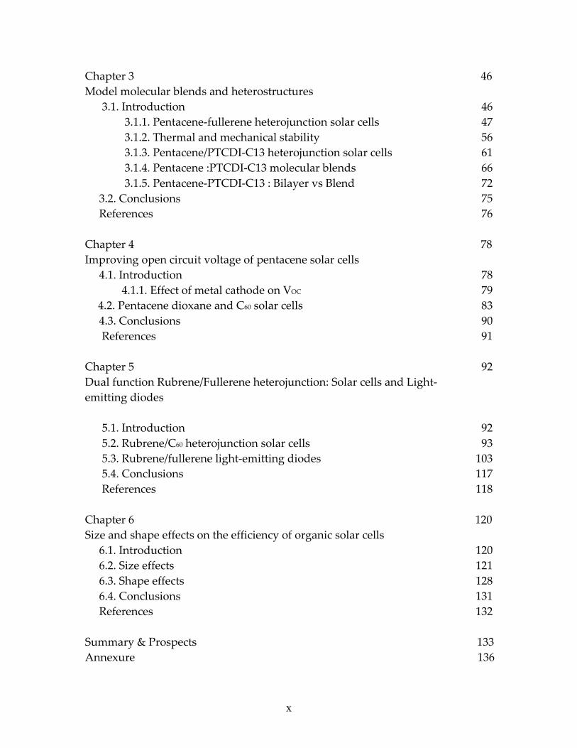


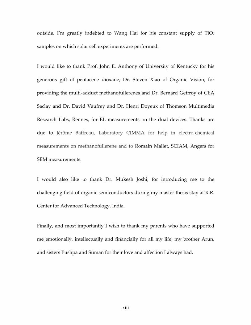

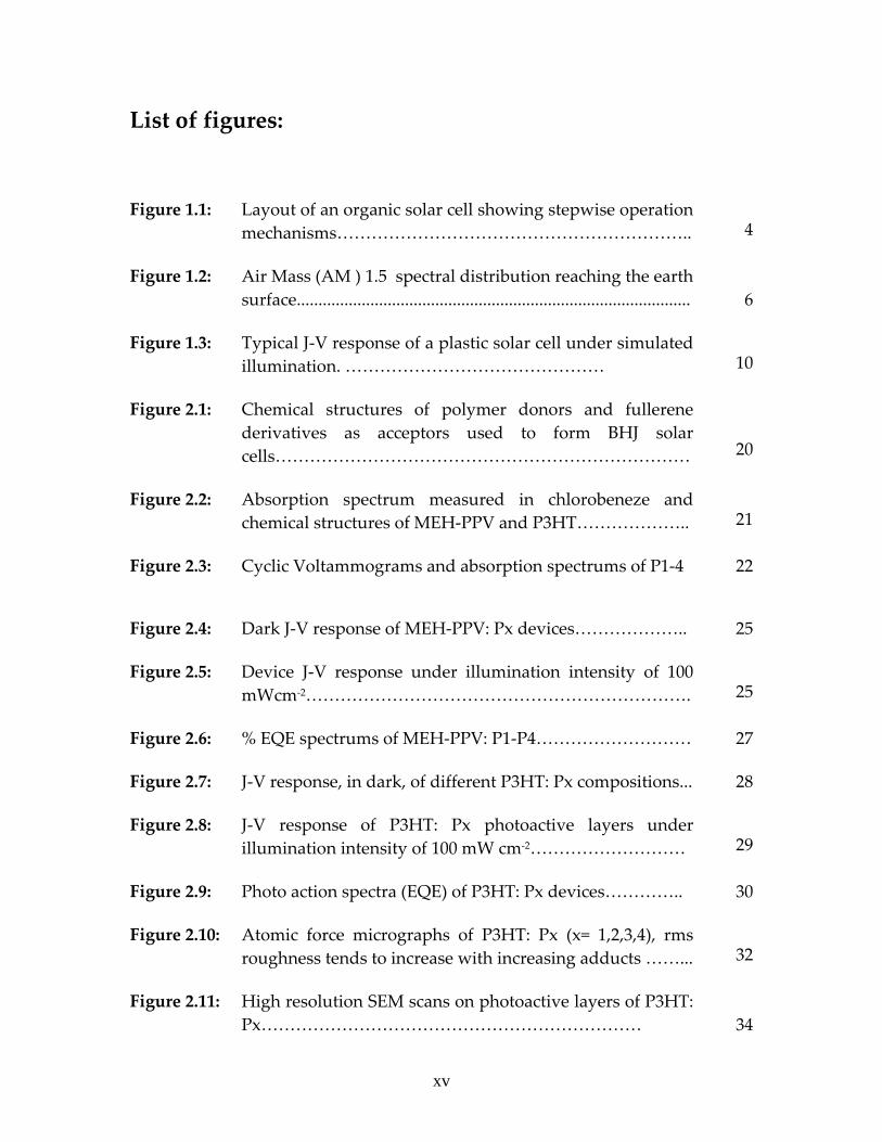
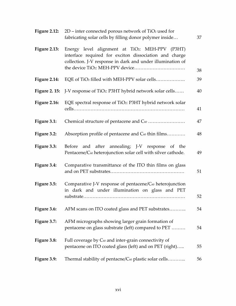


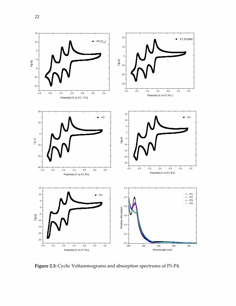


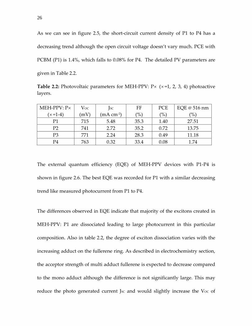
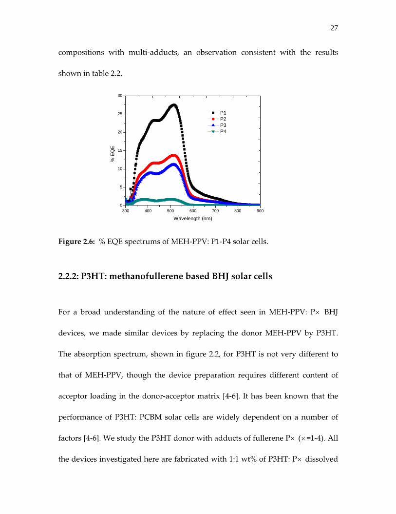
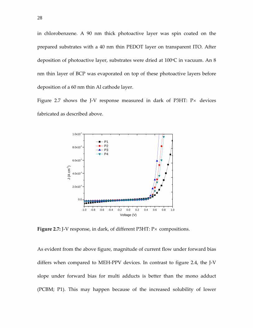


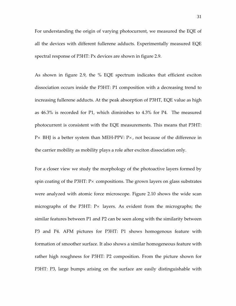


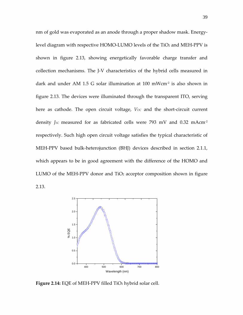


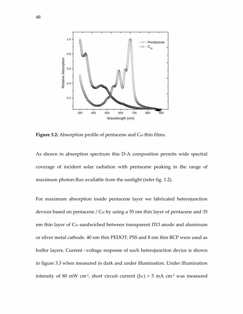
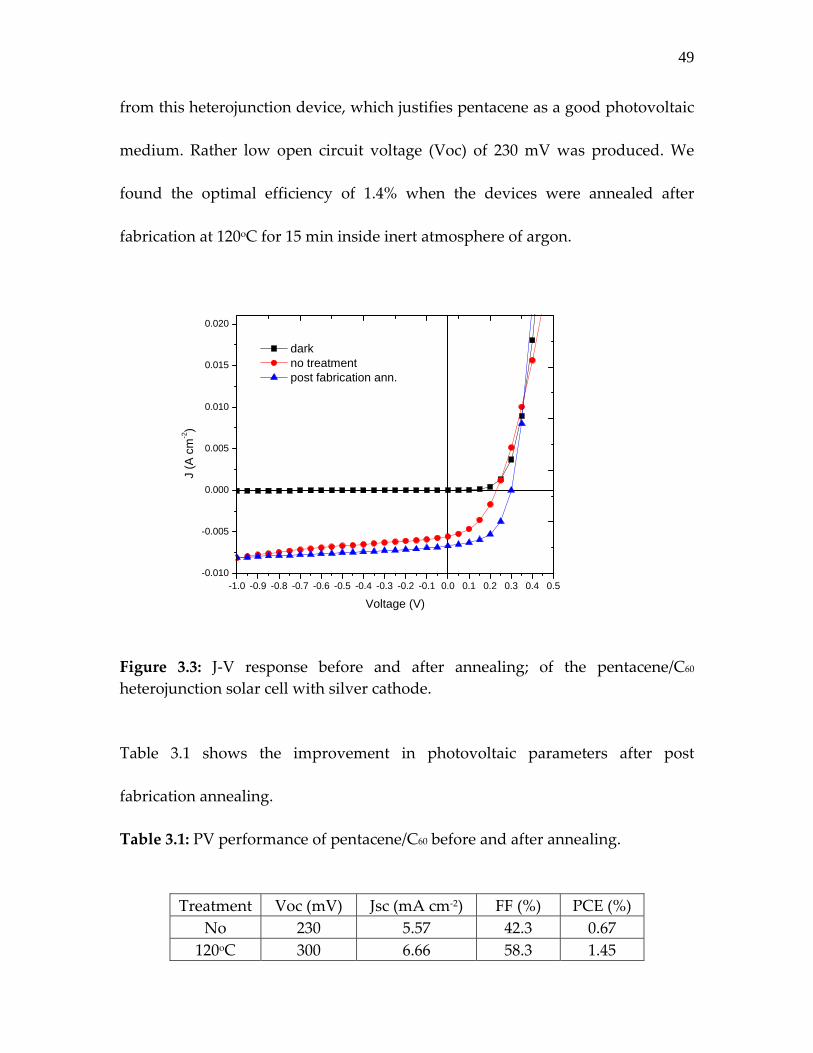


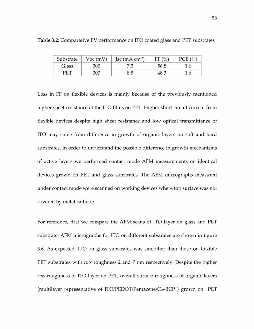


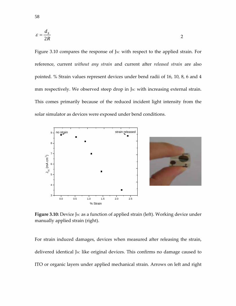

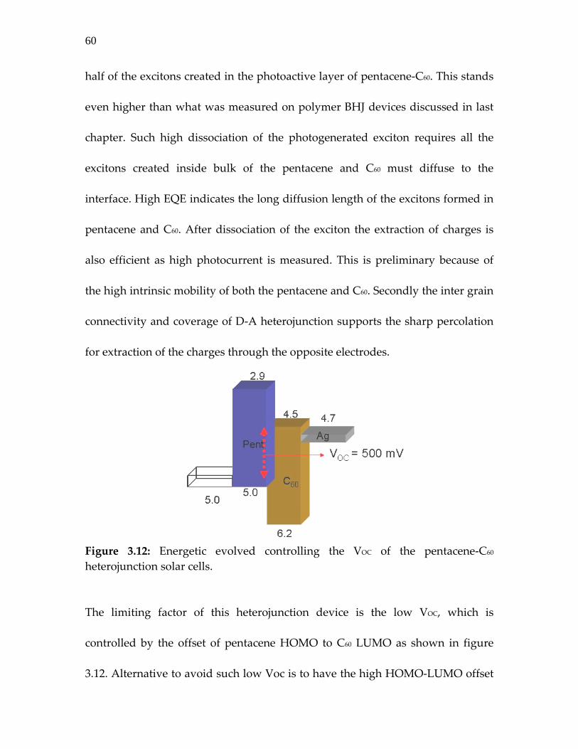
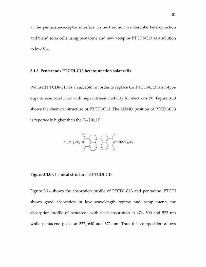
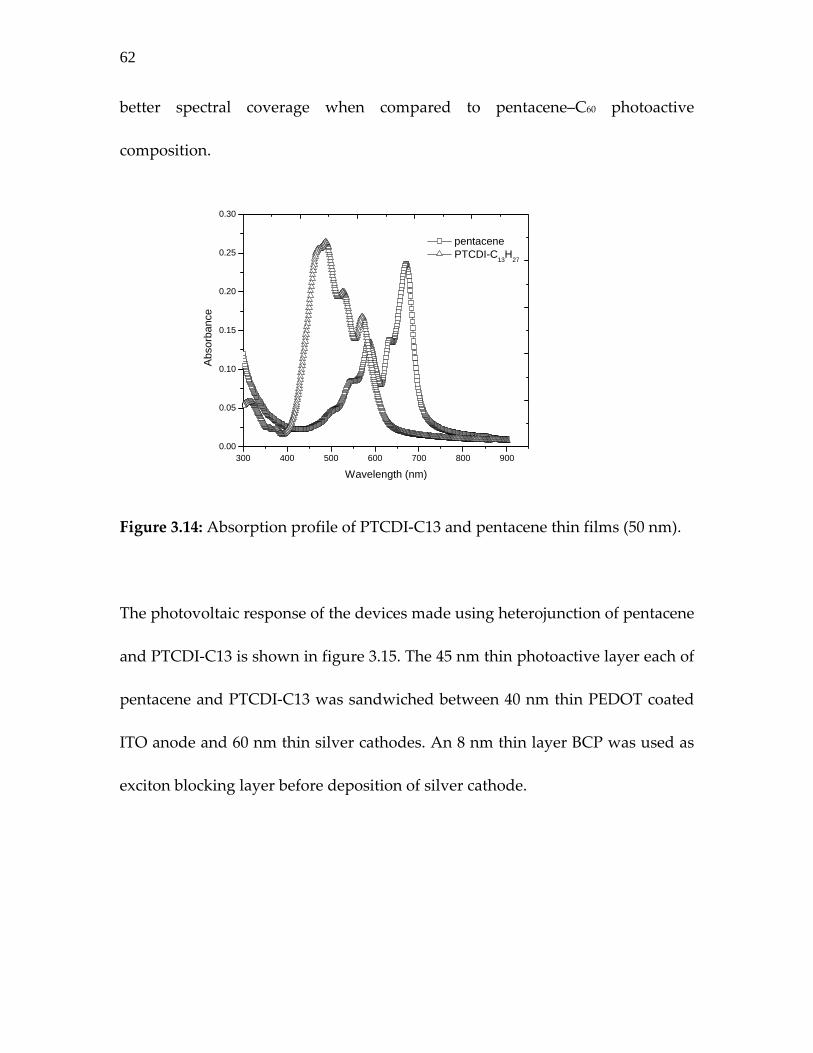

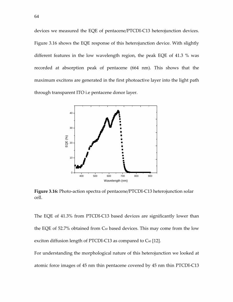
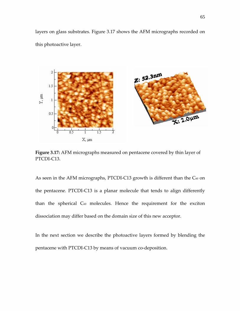

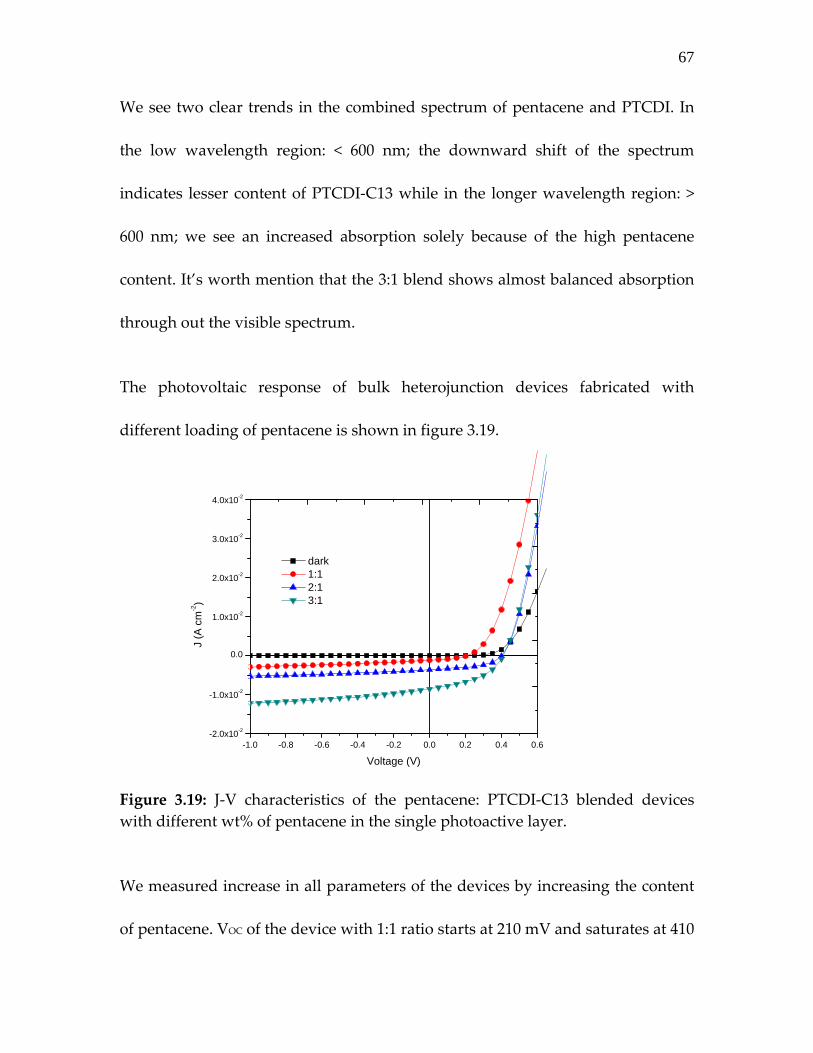
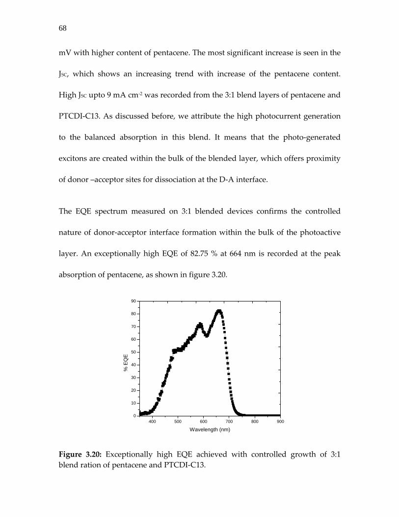
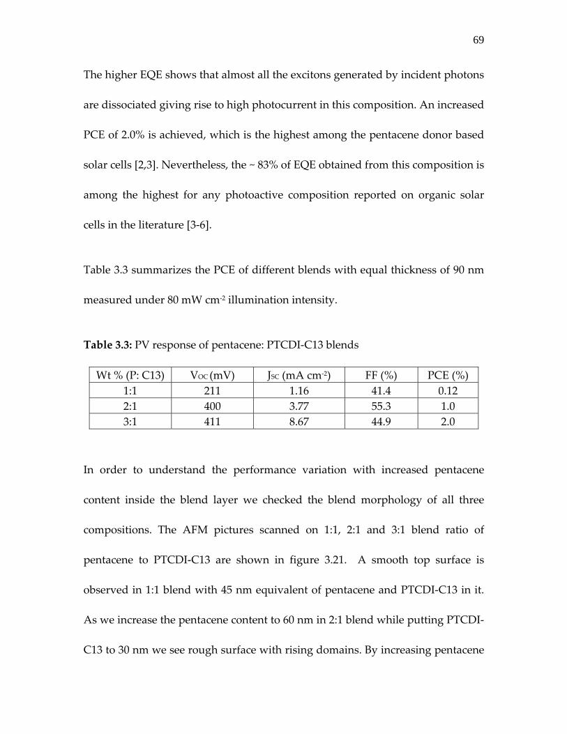


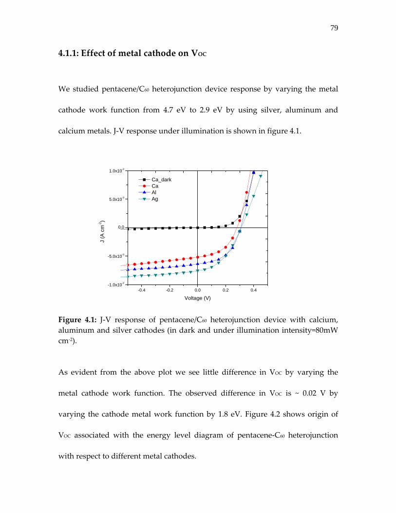

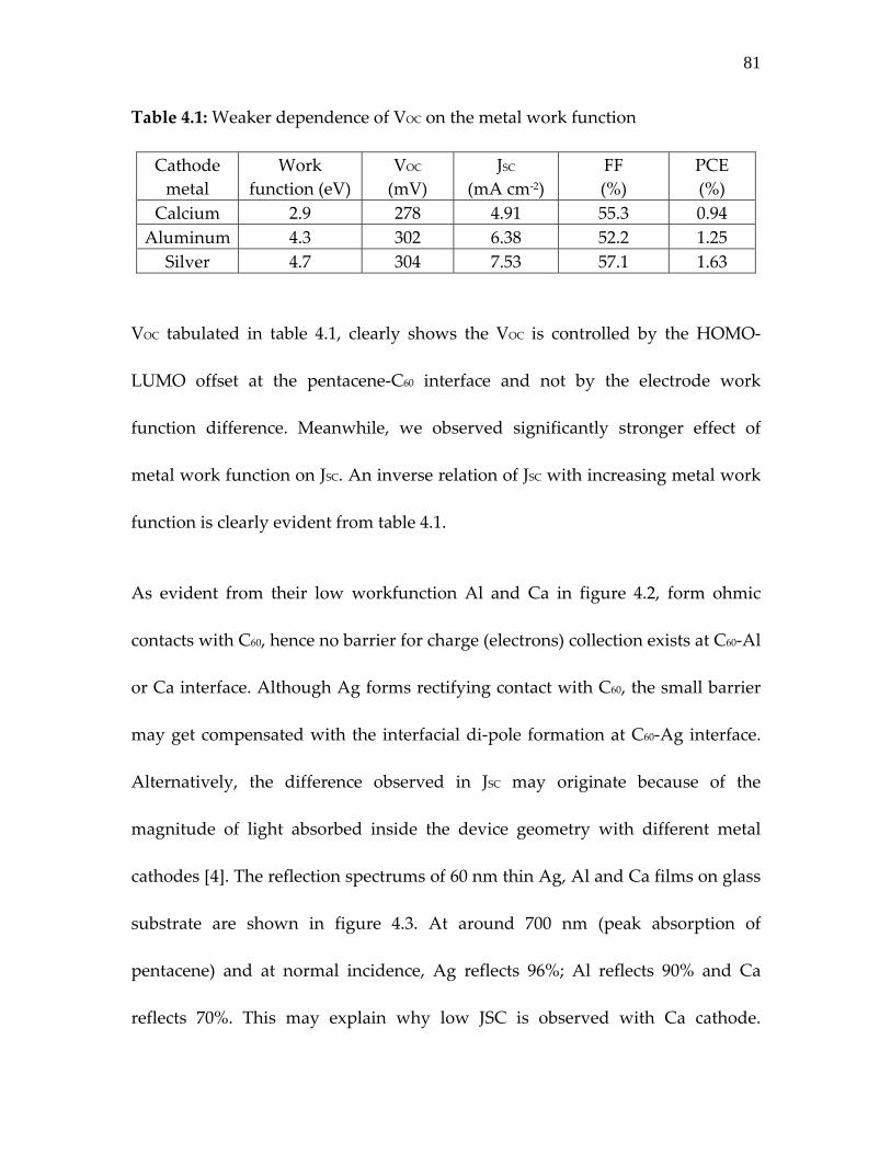


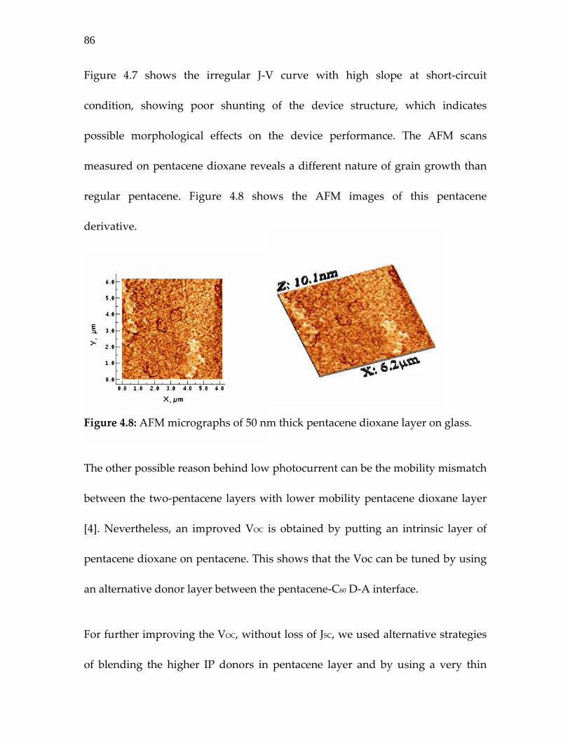
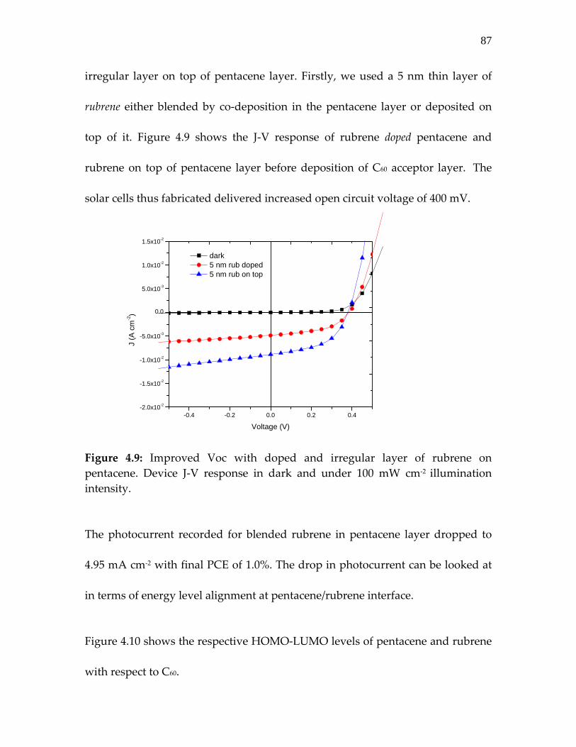

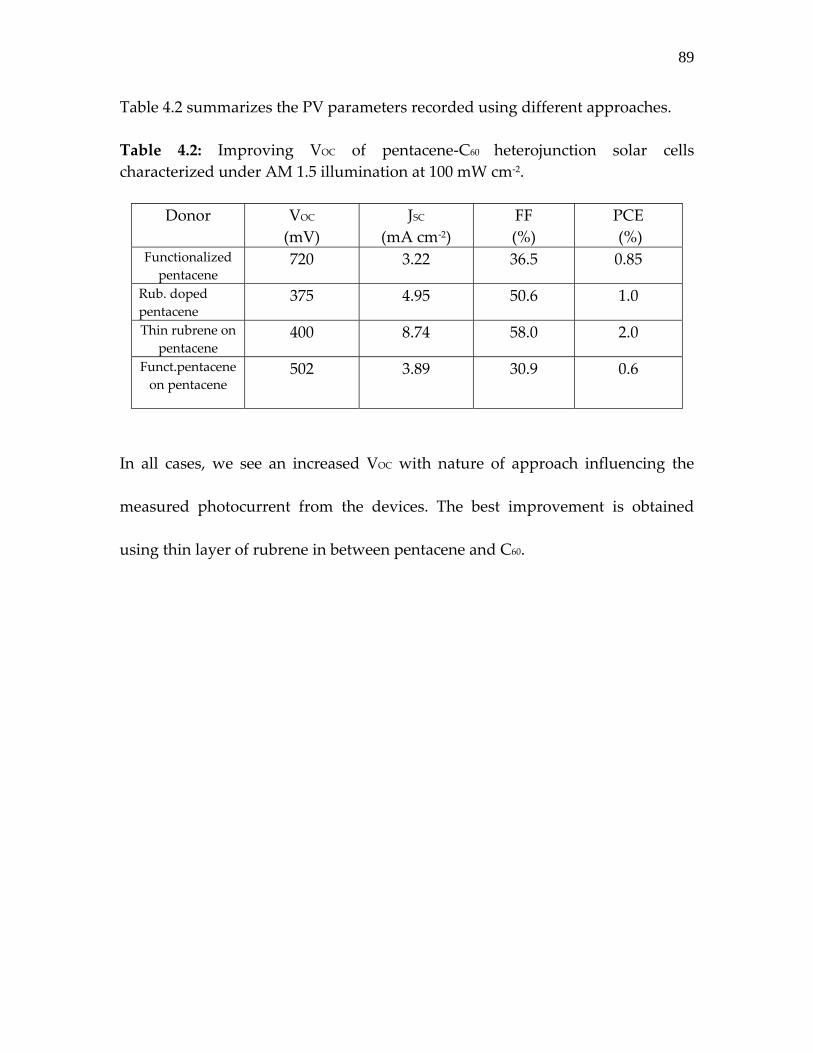

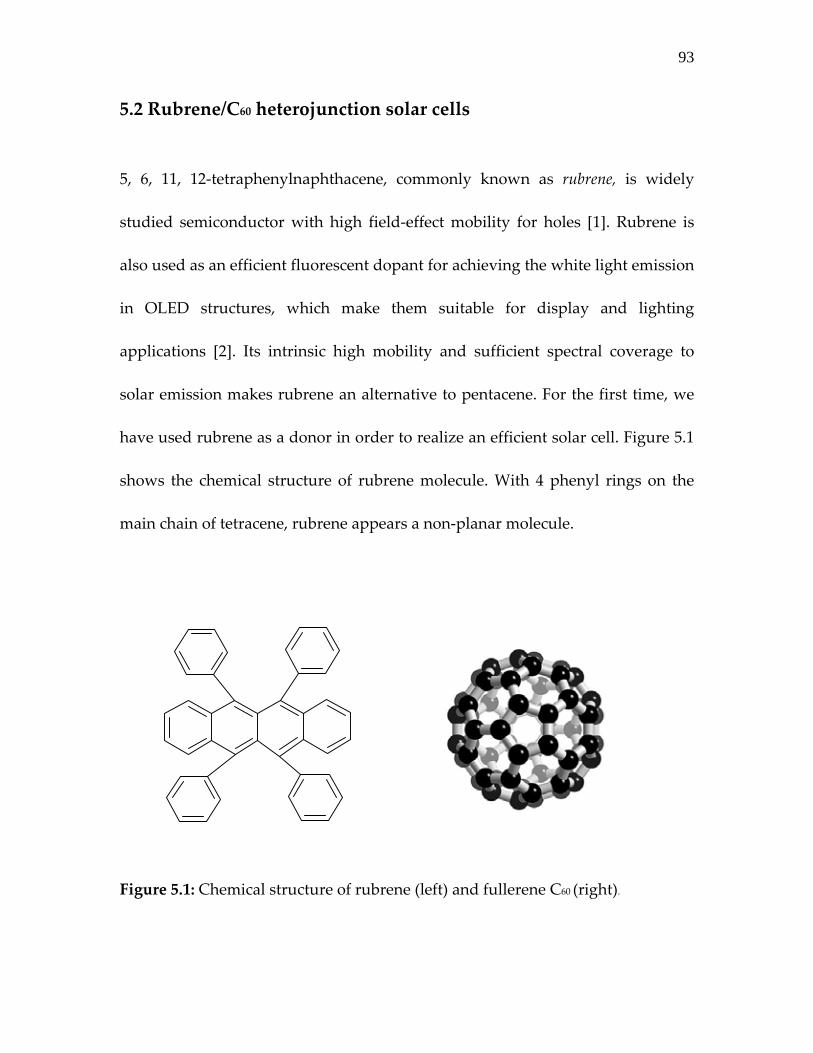

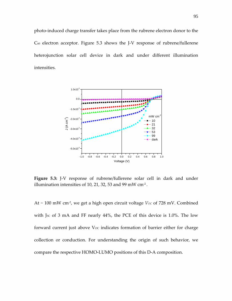

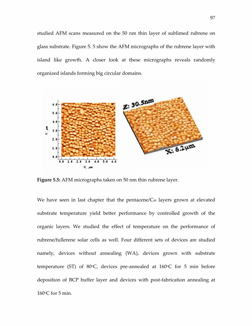
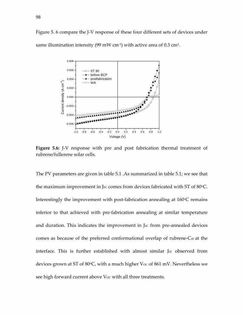
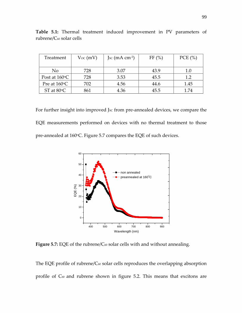


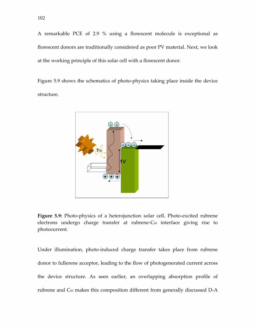
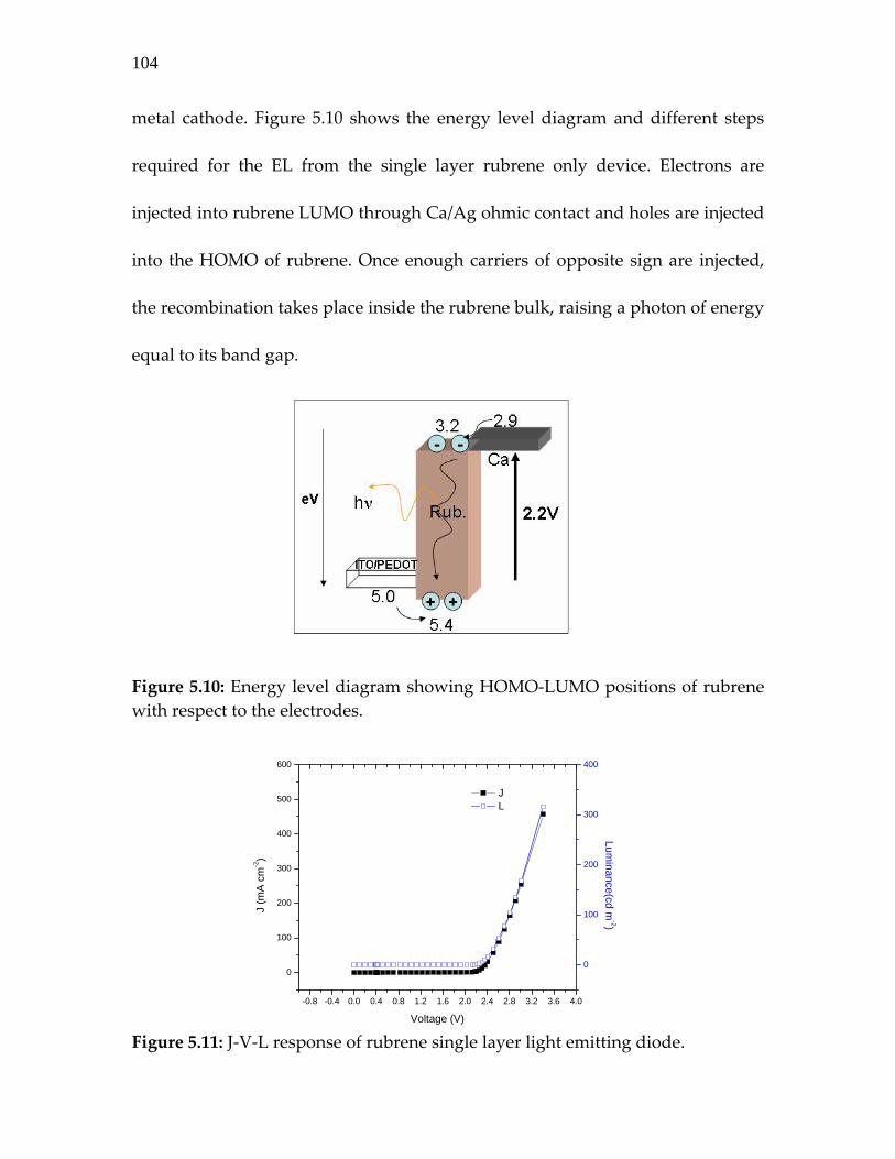
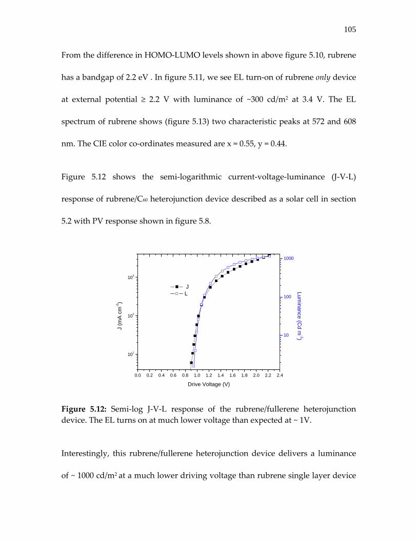
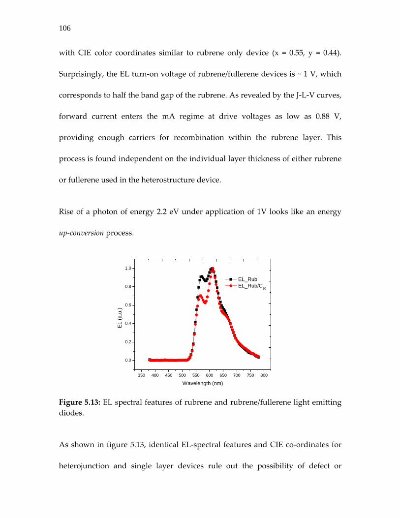


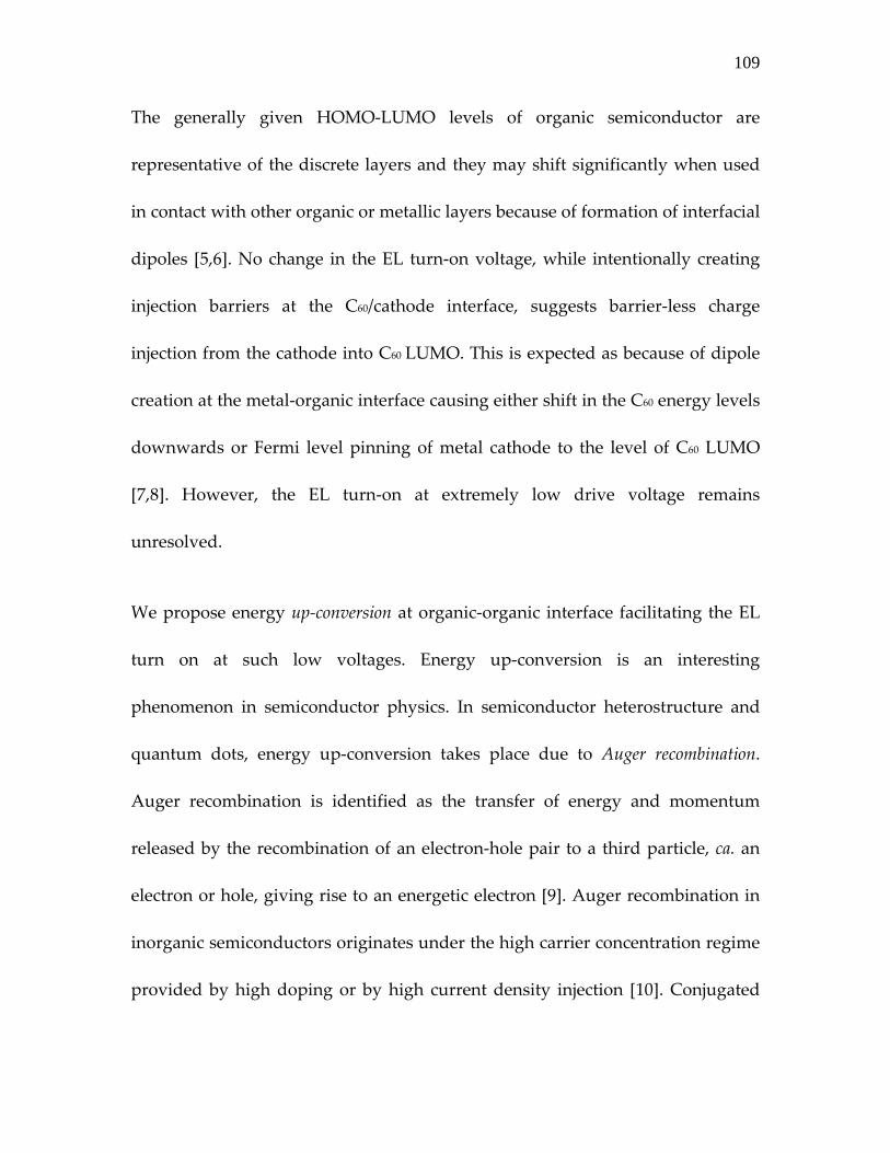
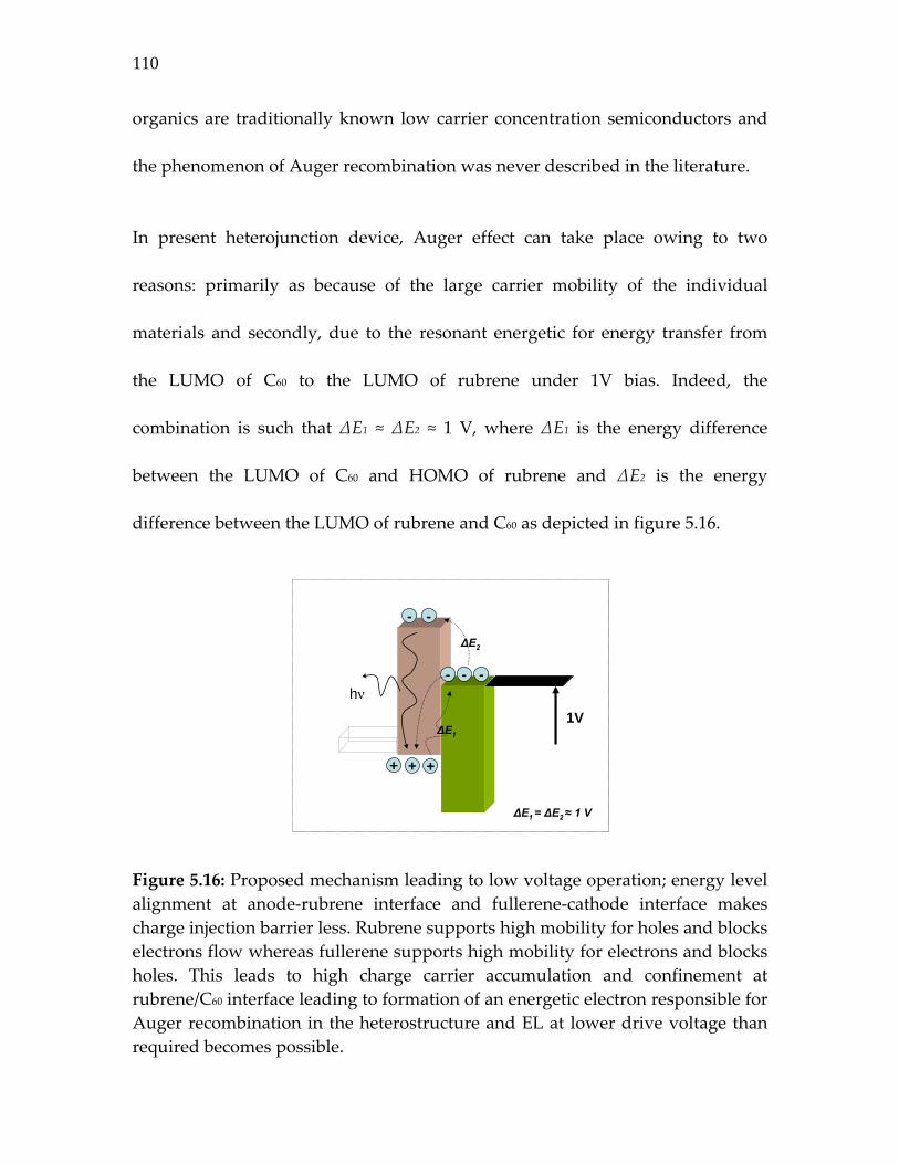
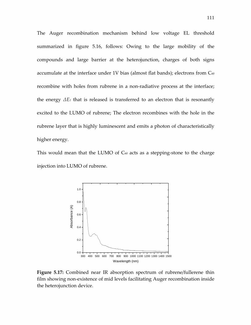


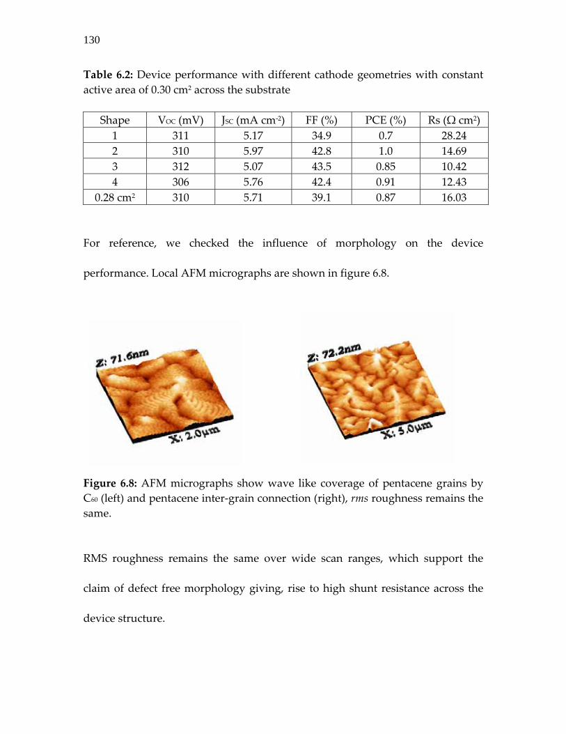


![CLASSIFICATION des DISPOSITIFS MEDICAUX … · CLASSIFICATION des DISPOSITIFS MEDICAUX ... et pour les médicaments : ... • SOUS-FAMILLE classe thérapeutique [2 C : < 50]](https://static.documents.pub/doc/80x56/5b8f4f0109d3f20e308c3139/classification-des-dispositifs-medicaux-classification-des-dispositifs-medicaux.jpg)


