inside News Review, News Analysis, Features, Research Review, and much more... Free Weekly E News round up go to: www.siliconsemiconductor.net Ensure Wet Process Cleaning Success OLED’s lighting and screen technology Structural Defects in a TO-220 Uncovering the Path to R&D Programmes Rely on SAM for 3D package analysis Plasma Dicing Technology By Panasonic Volume 41 Issue II 2020 @siliconsemi www.siliconsemiconductor.net
Transcript
inside News Review, News Analysis, Features, Research Review, and much more...Free Weekly E News round up go to: www.siliconsemiconductor.net
Ensure Wet Process Cleaning Success
OLED’s lighting and screen technology
Structural Defects in a TO-220
Uncovering the Path to R&D Programmes
Rely on SAM for 3D package analysis
Plasma Dicing TechnologyBy Panasonic
Volume 41 Issue II 2020 @siliconsemi www.siliconsemiconductor.net
We strive for accuracy in all we publish; readers and contributors are encouraged to contact us if their recognise an error or omission. Once a magazine edition is published [online, in print or both], we do not update previously published articles to align old company names, branding, marketing efforts, taglines, mission statements or other promotional verbiage, images, or logos to newly created or updated names, images, typographic renderings, logos (or similar) when such references/images were accurately stated, rendered or displayed at the time of the original publication. When companies change their names or the images/text used to represent the company, we invite organizations to provide Angel Business Communications with a news release detailing their new business objectives and/or other changes that could impact how customers/prospects might recognise the company, contact the organization, or engage with them for future commercial enterprise.
Publisher & Editor Jackie Cannon [email protected] +44 (0)1923 690205Technical Editor Mark Andrews [email protected] Sales & Marketing Manager Shehzad Munshi [email protected] +44 (0)1923 690215USA Representatives Tom Brun Brun Media [email protected] +001 724 539-2404 Janice Jenkins [email protected] +001 724-929-3550Director of Logistics Sharon Cowley [email protected] +44 (0)1923 690200Design & Production Manager Mitch Gaynor [email protected] +44 (0)1923 690214Circulation Director Scott Adams [email protected] +44 (0)2476 718970Chief Executive Officer Stephen Whitehurst [email protected] +44 (0)2476 718970
Joint Managing Director Sukhi Bhadal [email protected] +44 (0)2476 718970 Joint Managing Director Scott Adams [email protected] +44 (0)2476 718970 Directors Jackie Cannon, Sharon Cowley
Published by Angel Business Communications Ltd, Unit 6, Bow Court, Fletchworth Gate, Burnsall Road, Coventry CV5 6SP, UK. T: +44 (0)2476 718 970 F: +44 (0)2476 718 971 E: [email protected]
Silicon technologies and 2020’s new normalIN THE RECENT PAST, the debut of new work-from-home products were welcome additions to a global portfolio of chip-enabled solutions. Yet these products hardly gained the notoriety that they do today. Six months ago, only epidemiologists used the word ‘pandemic.’ Now, more than a third of tech employees are working from home. This is 2020’s New Normal.
While many of us are still trying to achieve balance between important and sometimes conflicting objectives, the pandemic has given us all a new perspective on what is important including the health we used to take for granted, family connections, and a collective future that is still being written.
No matter what is happening around us, technology continues to be a societal ‘glue’ that enables all types of work and life scenarios that were not imaginable mere months ago. I’m reminded of a former colleague from the Old School of business – He proudly called himself a Luddite – although a fantastic managers’ role model, he couldn’t quite get the knack of email. Today, he would flounder and fail. Even while tech industries face unprecedented challenges and opportunities, tech has emerged as the means by which we do business – We find community in team video conferencing; we find hope in social media posts by friends and family.
In this issue of Silicon Semiconductor, PVA TePla offers new insights into ways to test and inspect 3D packages through the use of scanning acoustic microscopy. JST provides insights into why effective wafer cleansing is critical to enabling
smaller device geometries. We look at more efficient, highly accurate wafer singulation technologies from Panasonic that reduce waste and increase throughput. We also explore ways that organizations often face gaps in their institutional knowledge when seasoned professionals retire or move on to new corporate homes. The article exploring ‘Dark Data’ from camLine discusses how an erosion of institutional knowledge can lead to repeats of failed experiments, while preserving this know-how can accelerate innovation.
‘Business Unusual’ has challenged us like never before. But we have also seen resilience across industries, demonstrating how we can productively live and work safely, even within our very changed world. Stay safe!
4 WWW.SILICONSEMICONDUCTOR.NET l ISSUE II 2020 l COPYRIGHT SILICON SEMICONDUCTOR
VOLUME 41 ISSUE II 2020
CONTENTS
18 Structural defects in TO-22 Ultrasound and X-ray work together to image and evaluate harmless anomalies and potential field failures in a TO-220 package.
22 Wet process cleaning equipment success Expert consultation can keep semiconductor production on track through installation and beyond.
26 Carrier profiling in high vacuum using SSRM and SCM Scanning Spreading Resistance Microscopy (SSRM) and Scanning Capacitance Microscopy (SCM) are both established scanning probe-based methods for two-dimensional carrier profiling.
32 Enabling smaller, lower- power IoT & wearables SiTimes makes a case for MEMS oscillators versus quartz-crystal–based clocking sources.
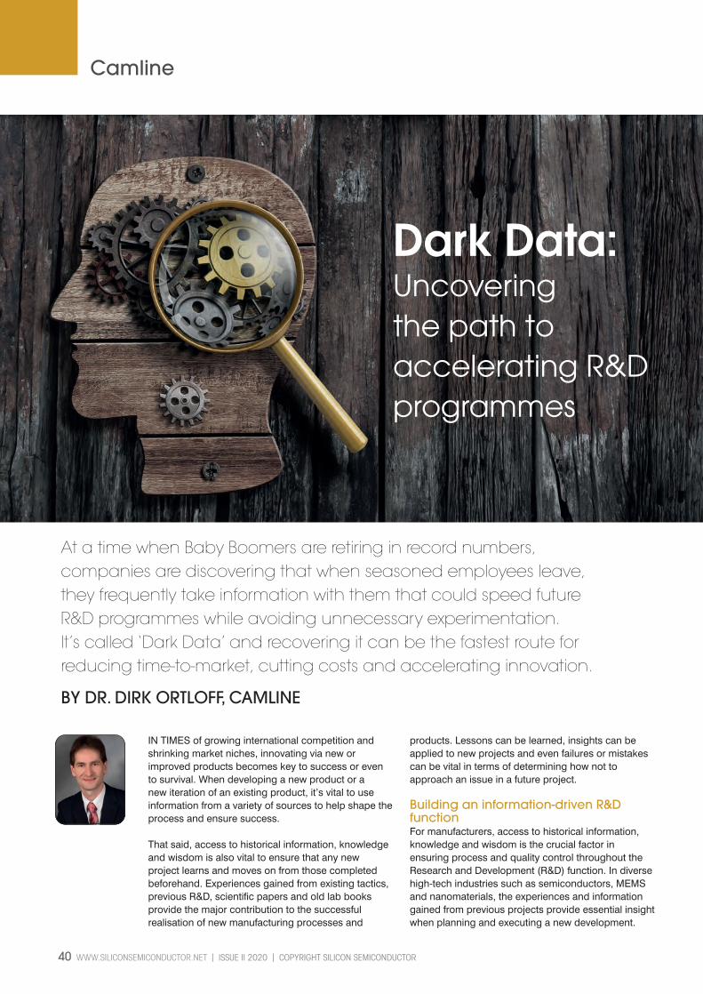
40 Dark Data: Uncovering the path to accelerating R&D programmes At a time when Baby Boomers are retiring in record numbers, companies are discovering that when seasoned employees leave, they frequently take information with them that could speed future R&D programmes while avoiding unnecessary experimentation.
44 Rely on SAM for 3D package device analysis The emergence of highly accurate wafer bonding and die stacking has enabled new generations of 3D semiconductors.
12 COVER STORY Panasonic’s plasma dicing for higner throughput and increased yield per wafer Plasma dicing addresses the challenges of dicing smaller and thinner dies
6 WWW.SILICONSEMICONDUCTOR.NET l ISSUE II 2020 l COPYRIGHT SILICON SEMICON DUCTOR
news reviewsSUSS MicroTec and Micro Resist Technology partner in advancing nanoimprint lithographySUSS MicroTec, supplier of equipment and process solutions for the semiconductor industry, and micro resist technology GmbH, a leading company for the development and production of innovative photoresists and advanced nanoimprint materials, announced today their cooperation on Nanoimprint Lithography (NIL).
NIL is a key enabler of the additive manufacturing revolution through high-fidelity pattern transfer. This UV-curing stamping process is increasingly used in the production of future emerging application in photonics, such as diffractive optical elements in augmented reality glasses or for face recognition as well as for the transfer of micro- and nanoscale structures, e.g. in optical sensors, laser nano-PSS (Patterned Sapphire Substrates) or for anti-counterfeiting.
The requirements for nanoimprint lithography and its applications are continuously changing. Therefore, the fundamental objective of the cooperation is to understand newly emerging requirements and to solve them by implementing solutions at both process and materials level, thus addressing the
high challenges set by the players in this industry. High quality imprint is based on three pillars: equipment, process and materials. The first two pillars, equipment and high-volume process manufacturing expertise, are addressed within the SUSS Imprint Excellence Center, a combined venture of SUSS MicroTec Lithography GmbH and SUSS MicroOptics SA. This constellation is further complemented and strengthened by joining the third pillar: the chemical expertise of the nanoimprint material supplier micro resist technology GmbH. The combination of these three pillars allows to better serve the high demanding need of the industry with its ever more challenging requirements on the replication of nanostructures.
“The SUSS Imprint Excellence Center leverages on decades of experience in imprinting equipment together with broad industrial process development in high-volume manufacturing environment,” said Franz Richter, CEO of SUSS MicroTec, “Further strengthening this cluster through a strong partnership with a leading resist supplier and experienced material manufacturer is mandatory in order to enable the perfect imprinting solutions.”
Involved companies are dedicated to pursue the deepening of their cooperation, with the common goal, to push further the development of existing and new applications towards both high performance and high volume production.
“For more than two decades, micro resist technology has provided tailor-made resist formulations for NIL around the globe”, said Ms. Gabi Grützner, CEO and founder of MRT. “Our profound know-how on polymer chemistry and replication processes allows us to provide state-of-the-art material solutions which addresses a growing number of industrial use-cases where replication technology is applied for the manufacturing consumer products.
“We are delighted about the cooperation with our partner within the alliance since our customers success of industrial imprint processes can be streamlined when materials and equipment are attuned to each other. This is the great opportunity we see in the SUSS Imprint Excellence Center as the right package is delivered to the community to make NIL available to more industrial users.”
Picosun Group reports excellent results in ALD-organic bilayer encapsulation of metal electrodes for neuroprosthetics and bioelectronic medicine. Group also reports superior hermetic barrier performance of its ALD nanolaminates against corrosive ion diffusion in aqueous media. This is an important result for medical ALD applications and implantology, where metal components and sensitive microelectronics need to be protected against corrosion caused by human body fluids.
Picosun’s ALD nanolaminates were proven to completely block the diffusion of Na+, K+, Cl- and PO43- ions, which are known to be amongst the most corrosive ionic species in aqueous media [1]. Tests were performed at 87 °C PBS
(phosphate-buffered saline) solution for 2 months (see Figure 1). Several of Picosun’s ALD materials have been proven non-cytotoxic and safe for human tissues already earlier [2], which gives great flexibility for designing tailored nanolaminate encapsulants for varying substrates and levels of protection.
For (platinum) metal electrode protection, ALD HfO2 was first used as an attachment and innermost barrier layer deposited right against the metal, and biocompatible organic polymer PDMS (polydimethylsiloxane) was applied on top of the ALD film to create impermeable, stable bilayer protection combing the best properties of both materials [3]. ALD HfO2 provides good adhesion to and hermetic sealing of the
surface, whereas PDMS, as the more “macroscopic” layer, robustness and sturdiness on top of the ultra-thin ALD film. The bilayer coatings were tested by soaking them in PBS solution for 450 days at room temperature.
The results of both tests again support ALD’s enormous potential to provide totally new solutions to the challenges medical device industries are facing. The constant trend of increased miniaturization and system-level integration of microelectronics drives the same development in implantable medical devices as well. When the device size decreases but its complexity and the time the device spends inside human body increase, traditional encapsulation methods fail.
COPYRIGHT SILICON SEMICONDUCTOR l ISSUE II 2020 l WWW.SILICONSEMICONDUCTOR.NET 7
news review sOnto Innovation announces three new metrology systemsONTO INNOVATION INC. announced the availability of a suite of process control metrology solutions for advanced device manufacturing. The suite of optical metrology solutions was developed for next generation semiconductor devices to enable high precision, high accuracy, and high productivity solutions for Gen6, 3D NAND, leading 5nm/3nm logic and advanced 1alpha DRAM devices.
This new metrology suite represents the first exciting results from Onto Innovation’s enhanced R&D team to create a comprehensive solution set that capitalizes on its extensive leadership in optical metrology and enhancements in a new machine learning engine software for all of these applications.
Kevin Heidrich, senior vice president of marketing, commented, “We are very excited by our customers’ early responses to the performance and value of these new systems. Our measurement data analysis from advanced logic and memory devices has been found to be highly correlated to our customers’ metrology lab standards such as CD-SEM and TEM, which means they can continue to use high-speed optical metrology systems without the need to use significantly slower, and more costly, X-ray technology.”
He continued, “For the most advanced 3D NAND devices, the challenges to measure the very high aspect ratio channel holes and word lines, with aspect ratios much greater than 80:1, are forcing customers to consider slower X-ray tools and other destructive measurement techniques. Similarly, for the most advanced DRAM and logic devices, complex transistor structures and new materials at the 5nm and 3nm nodes have customers looking at new methods of metrology for the critical gate-all-around/nano-sheet processing steps. Onto Innovation has developed platforms that drive optical technology to the next level enabling the advantages of both high sensitivity and high productivity, providing customers information at the rate and quality that
is needed for process development and high-volume manufacturing.”
The new Atlas V metrology system is designed to measure several key steps that include buried features, not visible by CD-SEM and other techniques. The sensitivity of Atlas V metrology enables these critical dimensions to be measured with high accuracy and sensitivity, extending the capability of optical solutions for generations of devices and eliminating the need for other slower process control techniques.
Atlas V technology now enables the performance needed for customers’ development of gate-all-around devices and is over 100 times faster than X-ray solutions for these structures. Onto Innovation’s customers that have validated this new OCD technology and have already seen the speed and resolution that was once thought to be beyond the limits of optical technology.
The IMPULSE V system, built on a history of industry leading reliability, enables higher productivity and higher performance for next generation integrated metrology. The system is designed to work seamlessly with chemical mechanical polishing (CMP) systems to provide high throughput run-to-run control for critical process steps. The IMPULSE V system enables recipe inter-operability with the Atlas V system for uninterrupted production recipe setup and optimization. Utilizing the latest machine learning technology, the IMPULSE V technology supports on-device metrology enabling broad flexibility and high process coverage
enabling higher productivity with broader process recipe coverage.
The new Aspect metrology system is a revolutionary optical platform that is designed for the current and future challenges of advanced 3D NAND devices. Memory density increases with both layer-pair scaling and tier stacking for memory stacks well over 200 pairs. The Aspect technology was designed with these future architectures and scaling strategies in mind. Aspect metrology is demonstrating performance superior to X-ray systems across multiple customer devices through a revolutionary infrared optical system providing full profiling capability to enable critical etch and deposition control, with the speed and process coverage that customers require.
AI-Diffract Technology is the key component of the new solution suite. It is the software analysis engine powering all of these leading metrology systems. This new product now provides up to 90% faster time to solution using the AI-Diffract engine which extends the industry leading NanoDiffract® software by leveraging extensive machine learning capabilities along with high fidelity modeling. The result is a simultaneous improvement in metrology performance along with a significant time to solution reduction.
All products are shipping to select customers this quarter, with broad availability by the fourth quarter. The company expects revenue to begin in the fourth quarter and ramp in the first half of 2021.
8 WWW.SILICONSEMICONDUCTOR.NET l ISSUE II 2020 l COPYRIGHT SILICON SEMICON DUCTOR
news reviewsImec overcomes fundamental operation challenge for voltage controlled RAMAT the 2020 Symposia on VLSI Technology and Circuits, imec, a leading research and innovation hub in nanoelectronics and digital technologies, presents a deterministic write scheme for voltage-controlled magnetic anisotropy (VCMA) magnetic random access memories (MRAMs), obviating the need for pre-reading the device before writing. This significantly improves the write duty cycle of the memory, enabling ns-scale write speeds.
As a second improvement, a manufacturable solution for external-field-free VCMA switching operation was demonstrated. Both innovations address fundamental write operation challenges for VCMA MRAMs, making them viable candidates for future high-performance low-power memory applications.
Voltage-controlled MRAM operation has recently been introduced to bring down the power consumption of spin-transfer-torque MRAM (STT-MRAM) devices – which is a class of non-volatile, high-density, high-speed memories.
While writing STT-MRAM memory cells is performed by means of a current (injected perpendicular into a magnetic
tunnel junction), VCMA MRAM uses an electric field (hence, a voltage) for its write operation – which is far less energy consuming. Two basic components are required to switch from the parallel (P) to the antiparallel state (AP) (or vice versa): an electric field (across the tunnel barrier) to remove the energy barrier, and an external in-plane magnetic field for the actual VCMA switching.
Imec has now solved two fundamental operation challenges which have so far limited the write speed and manufacturability of VCMA MRAMs, respectively. The slow write operation relates to the unipolar nature of the VCMA MRAM device: the same polarity of write pulse is needed to transition from the parallel to the anti-parallel (P-AP) state as to switch from anti-parallel to parallel (AP-P) state.
Therefore, the memory cell needs to be ‘pre-read’ to know its state before writing – a sequence which significantly slows down the write operation. Imec has introduced a unique deterministic VCMA write concept that avoids the need for pre-reading: distinct threshold voltages are introduced for the A-AP and AP-P transitions by creating an offset in the
energy barrier. This offset is realized by implementing a small (e.g. 5mT) offset magnetic field (Bz,eff) in the VCMA stack design.
As a second improvement, imec embedded a magnetic hardmask on top of the magnetic tunnel junction. This eliminates the need for an external magnetic field during VCMA switching, improving the device’s manufacturability without degrading its performance.
The devices were fabricated using imec’s 300mm state-of-the-art technology infrastructure, proving their compatibility with CMOS technology. Reliable 1.1GHz (or ns-scale speed) external-magnetic-field-free VCMA switching was demonstrated with only 20fJ write energy. A high tunnel magnetoresistance of 246% and an endurance of more than 1010 have been achieved. Gouri Sankar Kar, Program Director at imec: “These characteristics bring VCMA MRAM performance beyond STT-MRAM operation, making the devices ideal candidates for high-performance, low-power and high-density memory application – serving advanced computational needs or analog compute-in-memory applications.”
GLOBALFOUNDRIES acquire land in NY for new manufacturing facilityGLOBALFOUNDRIES, the specialty foundry and the leading U.S. pure-play manufacturer of semiconductors, has announced it has secured a purchase option agreement for approximately 66 acres of undeveloped land adjacent to its most advanced manufacturing facility, Fab 8, in Malta, N.Y., near the Luther Forest Technology Campus (LFTC).
The land parcel is located at the southeast end of the New York State Energy Research and Development Authority (NYSERDA) Saratoga Technology + Energy Park (STEP) campus, adjacent to Stonebreak Road Extension, between GF’s Fab 8 facility and Hermes Road. Exercising the option to purchase the land and commencement of development to expand GF’s Fab 8 facility will be subject to zoning regulations and client demand. The parcel is being sold at Fair Market Value, with a purchase price determined by an independent appraiser. “Amid growing consensus in our nation’s capital for investment in semiconductor manufacturing, it’s more important than ever that we are ready to fast track our growth plans at GLOBALFOUNDRIES’ most advanced manufacturing
facility in the U.S.,” said Ron Sampson, senior vice president and general manager of U.S. Fab Operations at GF. “With this agreement option, we now have additional flexibility to expand our footprint and position Fab 8 for future growth in Saratoga County and New York State, while strengthening U.S. leadership in semiconductor manufacturing.”
“GLOBALFOUNDRIES continues to demonstrate its commitment to economic growth in Saratoga County and Upstate New York,” said Darren O’Connor, Malta’s Town Supervisor. “I am pleased to hear that this latest step will enable future growth opportunities for GLOBALFOUNDRIES for years to come.”GF employs nearly 3,000 people and has invested over $13 billion in Fab 8, its most advanced manufacturing facility in upstate New York. The company recently announced it is bringing its most advanced Fab 8 facility in upstate New York into compliance with both the U.S. International Traffic in Arms Regulations (ITAR) standards and the highly restrictive Export Control Classification Numbers (ECCNs) under the Export Administration Regulations (EAR).
COPYRIGHT SILICON SEMICONDUCTOR l ISSUE II 2020 l WWW.SILICONSEMICONDUCTOR.NET 9
news review sOLED rising market marks new era in lighting and screen technologyThe OLED panel market is forecasted to grow at a CAGR of 12.9% during 2020-2025 to reach 45.55 billion units by 2025. While there will be a slight downturn overall due to Covid-19 pandemic, industry experts continue to expect OLED panels to be a significant display technology trend adopted across the world, with larger screen sizes, improved 8K resolution and new form factors.
Atomic Force Microscope manufacturer, Park Systems has scaled up its AFM tools for Gen8+ and all large flat-panel displays with the Park NX-TSH (Tip Scanning Head) system. It is the industry’s only automated Tip Scan Head for analyzing samples larger than 300 mm. “Park NX-TSH is designed for large and heavy flat-panel display glass and 2D encoders, with integrated micro probe stations for conductive AFM and electric defect analysis,” explains Keibock Lee, Park Systems President. “Park NX-TSH can scan up to 100 µm x 100 µm (x-y direction) and 15 µm (z direction), and it has a flexible chuck to accommodate samples larger than 300 mm and heavier than 1 Kg—engineered for OLED, LCD and other large sample analysis.”
Organic Light Emitting Diode (OLED) technology is being used in an increasing number of application areas because they can be flat, paper-thin and flexible, and have the ability to diffuse light, which is expected to significantly drive the
market growth over the next few years.Park Systems, in anticipation of the market expansion, has developed Park NX-TSH specifically for manufacturers setting up fabs that produce next-generation flat-panel displays with the objective of overcoming the 300 mm sample size limit. Using conductive AFM, Park NX-TSH can measure the sample’s electrical properties by supplying current through the optional probe stations.
The enabling technology for Park NX-TSH is the tip scanning head attached to the gantry that moves to the desired measurement positions on the surface of the sample that is fixed on a sample chuck. The Park NX-TSH tip scanning head system therefore overcomes the limitations of sample size and weight.
OLEDs, the next advance in lighting, differ from LEDs in that the semiconductors used to convert electricity into light are not synthetic single crystals but rather films composed of organic molecules.
The organic component makes them lighter and more energy efficient. Large panels can be assembled and stretched into unique displays, enhancing architectural design. Furthermore, it is even more sustainable given that OLEDs do not contain mercury, so when in widespread use they can save enormous amounts of hazardous waste.
Park Systems Announces NanoScientific SymposiumPARK SYSTEMS will be presenting ‘NanoScientific Symposium on Nano Applications for a Changing World’ sponsored by Physics World and Nanotechnology World Association. It will be held online Oct. 14-15, 2020.
Park Systems launched this online event for researchers and scientists in nanoscience and nanotechnology to share data on how new nano applications under research will lead to discoveries that have positive impact on the world. The idea is that attendees will join together in a worldwide effort to understand to create breakthroughs in scientific discovery of how nanoparticles interact with matter and human physiology and how this knowledge can be harnessed to create a smarter future.
Nanometrology plays an important role in helping researchers understand how nanoparticles interact with matter, gas and the environment, showing in nano detail how individual cells react to various stimulus. Labs worldwide benefit from the advent of nanoscopic tools that give them clear images in real time.
“NanoTechnology World Association and Park Systems are showcasing the worldwide collaboration of our scientific communities to enrich our vulnerable planet and humanity with unprecedented scientific advances that inspire leadership roles in sustainability,” says Marine Le Bouar, CEO , Nanotechnology World Association.
The Symposium is accepting presentation abstracts. In an effort to expedite the abstract submission process, please send a short abstract (can be 300 words or less) about your work in nano materials by July 30, 2020. Submit your abstract to: [email protected]
10 WWW.SILICONSEMICONDUCTOR.NET l ISSUE II 2020 l COPYRIGHT SILICON SEMICON DUCTOR
news reviewsACM Research launches 18-chamber single-wafer cleaning toolACM Research, Inc, a supplier of wafer cleaning technologies for advanced semiconductor devices,has announced from SEMICON China its Ultra C VI single wafer tool, the newest addition to its line of Ultra C cleaning systems. The Ultra C VI targets high-throughput cleaning of dynamic random-access memory (DRAM) and 3D NAND Flash devices to support increased production scale. Building on ACM’s proven multi-chamber technology, the new tool features 18 chambers, representing a 50-percent expansion on the throughput and 12 chambers included in the Ultra C V system, with the same tool width and only slightly larger in length to allow for integration into existing production lines.
“Although memory devices are increasing in complexity, they still have the same high throughput requirements,” said ACM’s president and CEO Dr. David Wang. “Additional cleaning chambers enable memory device makers to support extra processing steps and more sophisticated drying technology, while maintaining or reducing production cycle time. We see an 18-chamber configuration as the sweet spot for this application. Compared to systems with higher chamber counts, the Ultra C VI
provides a better balance for wafer-per-hour requirements and factory-automation matching.”
The Ultra C VI performs single-wafer cleaning for advanced DRAM devices of 1y nm and beyond, as well as advanced 3D NAND devices with 128 stacked layers and above. It can be used for a variety of front-end-of-line (FEOL) and back-end-of-line (BEOL) processes, depending on the application and the chemistries involved, such as BEOL polymer removal, tungsten- or copper-loop post-cleans, pre-deposition cleans, post-etch and post-chemical mechanical planarization (CMP) cleaning, deep-trench/via cleans, and RCA standard cleans.
Multiple chemical combinations can be used during cleaning, including standard clean (SC1, SC2), hydrofluoric acid (HF), ozonated deionized water (DI-O3), diluted sulfuric peroxide mixture (DSP, DSP+), solvent cleaner, or other process chemicals. Up to two chemicals can be reclaimed and reused, which helps reduce the cost of consumables and overall cost of ownership. The Ultra C
VI can accommodate optional physical assistant cleaning methods, such as dual-fluid N2 spray cleaning or ACM’s proprietary SAPS and TEBO megasonic cleaning technologies. It also offers an isopropyl alcohol (IPA) drying function that can be applied to patterned wafers with high aspect ratios. Moreover, as it fits within the same width as ACM’s existing tools, this tool helps improve fab utilization and further contributes to lower cost of ownership. ACM plans to deliver the Ultra C VI tool to a leading memory manufacturer for evaluation and qualification in the third quarter of 2020.
Pfeiffer Vacuum introduces next generation gas analyzersOmniStar and ThermoStar GSD 350 are compact, portable benchtop analyzers for analyzing gases at atmospheric pressure. They are particularly used for applications in chemical processes, in the semiconductor industry, metallurgy, fermentation, catalysis, freeze-drying and environmental analysis. The gas inlet is fitted with a heated capillary for use at up to 350°C. This prevents vapors from condensing during process gas analysis. Thanks to the two-stage inlet system, an almost segregation-free gas supply is possible.
The ThermoStar solution was specially developed for coupling with thermo balances. The inlet system with a quartz capillary and a platinum orifice ensures that even the smallest concentrations
can be analyzed. The OmniStar was developed for a wide range of applications and uses a stainless steel capillary as well as a valve which can interrupt the sample gas stream. Unlike other analytical methods such as FTIR or GC-FID, the two new devices allow simultaneous detection of all gases within the mass range.
With the new PV MassSpec software, it is possible to perform qualitative and quantitative analyses. This software offers a clear and user-friendly platform for recording and displaying measurement data and parameter settings. Even complete measuring procedures can be programmed and automated. With a variety of equipment variants available, the mass ranges of 1 to 100 u, 1 to 200 u
and 1 to 300 u are covered. The two new models differ from comparable devices by their compact size and easy operation using an integrated 7ʺ touch display or a web user interface. The device can be fully controlled and the user can also perform simple measurements without a PC or PV MassSpec via a smartphone or tablet.
The low detection limit (depending on the mass range) of up to <100 ppb, the low gas consumption of 1 - 2 sccm and the fast measuring time (up to 1 ms/u) characterize the new analytical instruments. For extended process customization, an integrated mass calibration device or a controlled purge gas system for corrosive gases are available.
12 WWW.SILICONSEMICONDUCTOR.NET l ISSUE II 2020 l COPYRIGHT SILICON SEMICONDUCTOR
Panasonic Plasma DicingFor higher throughput and increased yield per wafer
Plasma dicing addresses the challenges of dicing smaller and thinner dies.
BY PANASONIC
EVERY PERSON with a passing interest in electronics has heard of Moore’s Law: the processing power of affordable CPUs – or the number of transistors on a chip - will roughly double every two years. It is credit to both Gordon Moore’s foresight, and the technical and engineering teams around the world who continue to innovate, that the ‘Law’ is still even being discussed today.
Part of the reason for chip size reduction lies in the shrinking of technology nodes (process geometries). Currently the smallest node that is being manufactured in mass volume is 7nm, and even smaller sizes are under development in the industry.The increase in processing power and speed and the miniaturisation and integration of electronic functions
that continue to result from such technological advances lie at the heart of the pervasiveness of electronics in our everyday lives: the smart phones that we rely on; the uptake of artificial intelligence in smart homes and cities; driverless vehicles; remote medical home diagnostics – there is not one aspect of life that electronic products and systems have not penetrated.
But for this to continue, it is not only in the area of photolithographic processing that technology needs to keep innovating. Once a wafer has been created it must be singulated into individual dies, and as dies are becoming smaller and thinner, many products are facing difficulties caused by the singulation or dicing process.
COPYRIGHT SILICON SEMICONDUCTOR l ISSUE II 2020 l WWW.SILICONSEMICONDUCTOR.NET 13
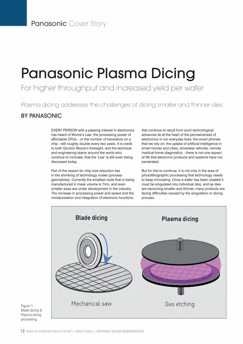
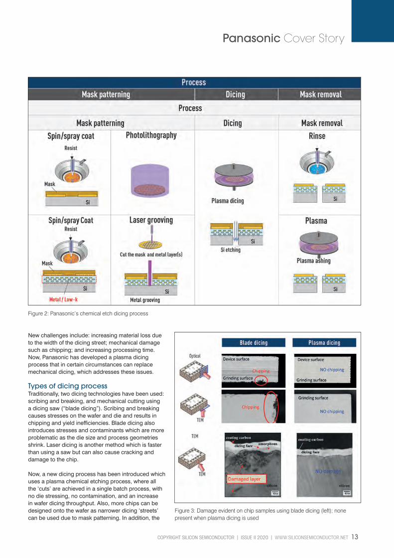
New challenges include: increasing material loss due to the width of the dicing street; mechanical damage such as chipping; and increasing processing time. Now, Panasonic has developed a plasma dicingprocess that in certain circumstances can replace mechanical dicing, which addresses these issues. Types of dicing processTraditionally, two dicing technologies have been used: scribing and breaking, and mechanical cutting using a dicing saw (“blade dicing”). Scribing and breaking causes stresses on the wafer and die and results in chipping and yield inefficiencies. Blade dicing also introduces stresses and contaminants which are more problematic as the die size and process geometries shrink. Laser dicing is another method which is faster than using a saw but can also cause cracking and damage to the chip.
Now, a new dicing process has been introduced which uses a plasma chemical etching process, where all the ‘cuts’ are achieved in a single batch process, with no die stressing, no contamination, and an increase in wafer dicing throughput. Also, more chips can be designed onto the wafer as narrower dicing ‘streets’ can be used due to mask patterning. In addition, the
Figure 2: Panasonic’s chemical etch dicing process
Figure 3: Damage evident on chip samples using blade dicing (left); none present when plasma dicing is used
14 WWW.SILICONSEMICONDUCTOR.NET l ISSUE II 2020 l COPYRIGHT SILICON SEMICONDUCTOR
mask pattern enables flexibility in the choice of chip sizes, shapes, positioning. The two approaches are shown in Figure 1.
Figure 2 shows Panasonic’s plasma dicing process which uses a dicing mask. The plasma process etches the streets by chemical reaction. Plasma dicing uses pulsed or time-multiplexed etching, with the process cycling repeatedly between two phases: a near-iso- tropic plasma etch where ions attack the wafer in a near-vertical direction; followed by the deposition of a chemically inert passivation layer which protects the entire substrate from further chemical attack.
During etching, the vertically-directed ions attack the passivation layer only at the bottom of the trench (not along the walls), exposing the substrate to the chemical etch. This two-phase process results in side-walls that increase and decrease with an amplitude of between 100 and 500nm. The cycle time is adjustable: short cycles yield smooth walls; longer cycles yield a higher etch rate.
Particle-free and damage-free processThe action of the saw blade during the dicing process causes mechanical damage and affects inner layers of the die. Figure 3 demonstrates damage and chipping at the edge and of the inner layers. By contrast, the micro-photographs show no damage when the individual dies are separated using the plasma dicing process. Also, unlike blade dicing which causes micro particles of the wafer (e.g. silicon) to be freed up, potentially causing devices to fail, by using plasma etching, no contaminating particles are released.
Greater chip strengthChip breakage tests show the typical range of fracture strength for silicon chips to be in the range of 100MPa up to 3000MPa. Dies from several positions on a 150µm thick wafer were sampled and a Weibull plot was used to compare the statistical data for chip strengths of lots using blade and plasma dicing preparation methods.
Figure 4: Strength tests prove the benefits of plasma dicing
Left: Figure 5: Productivity curves show increasing benefits with smaller chip
COPYRIGHT SILICON SEMICONDUCTOR l ISSUE II 2020 l WWW.SILICONSEMICONDUCTOR.NET 15
Figure 4 shows that the plasma dicing process results in chips that are about five times stronger than those which underwent blade dicing. With a fracture stress pressure of 600MPa, all samples of chips that had been processed using blade dicing broke due to internal micro- cracks, whereas all of the plasma diced chips shattered at a pressure close to the breaking-strength of silicon. Therefore the plasma dicing process is proven to result in dramatically higher chip strength, especially if thin wafers are being processed.
Higher throughput and yieldThe processing time of blade dicing depends on the number of dicing lines. If the die size is small, longer dicing processing time is required and throughput is reduced. However, with the plasma dicing process, etching is performed across the whole wafer in one pass, so throughput remains constant, no matter how many dicing streets are required (see Figure 5). In addition, the plasma dicing process uses a narrower dicing street design. With blade dicing, there is always a minimum cutting street width, due to the thickness of the blade. A simulation prepared by Panasonic shows that for a 0.5mm² chip size, reducing the dicing street width from 60µm to 5µm, yield will be increased by 23% using the new plasma process (see figure 6). However, the method of avoiding chips contacting other chips when handling a wafer with 5µm dicing street width needs to be considered.
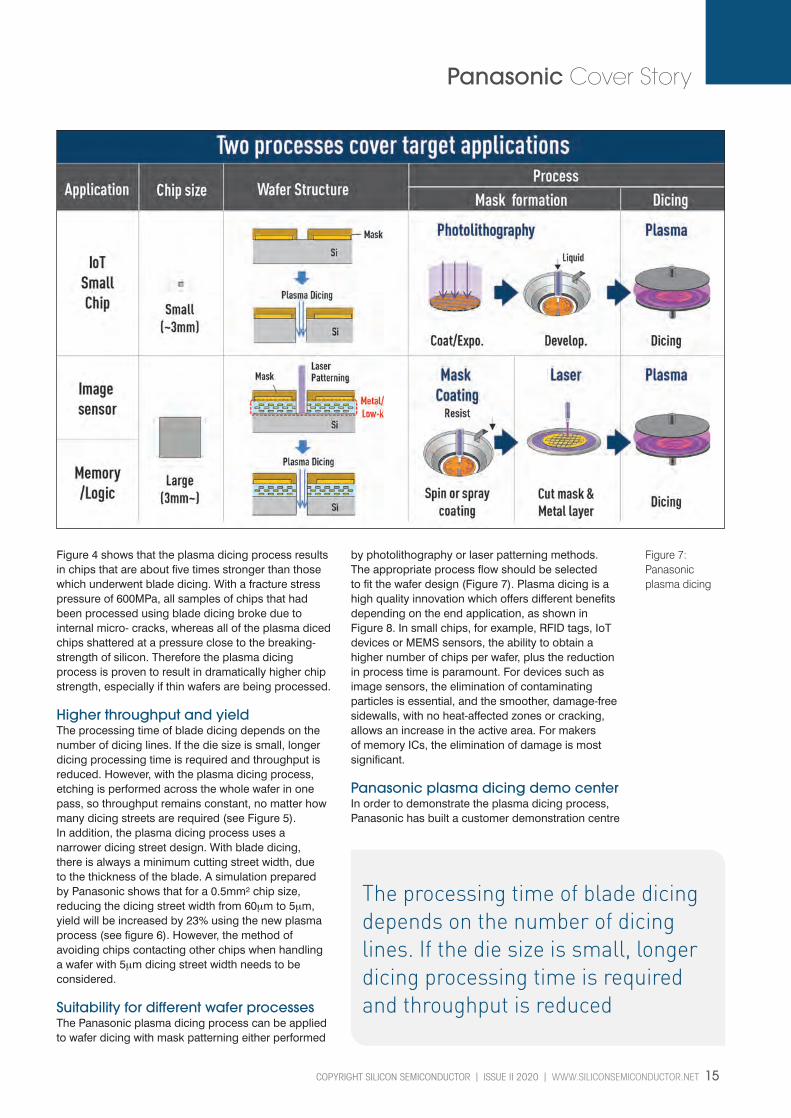
Suitability for different wafer processesThe Panasonic plasma dicing process can be applied to wafer dicing with mask patterning either performed
by photolithography or laser patterning methods. The appropriate process flow should be selected to fit the wafer design (Figure 7). Plasma dicing is a high quality innovation which offers different benefits depending on the end application, as shown in Figure 8. In small chips, for example, RFID tags, IoT devices or MEMS sensors, the ability to obtain a higher number of chips per wafer, plus the reduction in process time is paramount. For devices such as image sensors, the elimination of contaminating particles is essential, and the smoother, damage-free sidewalls, with no heat-affected zones or cracking, allows an increase in the active area. For makers of memory ICs, the elimination of damage is most significant.
Panasonic plasma dicing demo centerIn order to demonstrate the plasma dicing process, Panasonic has built a customer demonstration centre
Figure 7: Panasonic plasma dicing
The processing time of blade dicing depends on the number of dicing lines. If the die size is small, longer dicing processing time is required and throughput is reduced
16 WWW.SILICONSEMICONDUCTOR.NET l ISSUE II 2020 l COPYRIGHT SILICON SEMICONDUCTOR
in Osaka, Japan. This Class 1000 facility is capable of processing 200mm and 300mm diameter wafers with a minimum thickness of 25µm. It is fully-equipped including two APX300 plasma dicing machines, laser pattern- ing equipment, polisher / grinder, lithography and measurement equipment, enabling customers to quickly and thoroughly evaluate different products and materials.
Total Solutions ApproachIn addition to supplying the APX300 Plasma Dicer,
Figure 9: Summarises the different dicing processes and the advantages of the plasma dicing process
Panasonic is in close contact with vendors globally to assist our customers with the integration and selection of appropriate equipment and material, and implementation of decades of process know-how.
ConclusionPanasonic’s plasma dicing process achieves damage-free and particle-free dicing, resulting in inherently stronger chips and increased yield. Throughput is increased and production costs reduced.
18 WWW.SILICONSEMICONDUCTOR.NET l ISSUE II 2020 l COPYRIGHT SILICON SEMICONDUCTOR
Nordson Sonoscan
Structural defects in
TO-22Ultrasound and X-ray work together to image and evaluate harmless anomalies and potential field failures in a TO-220 package.
BY TOM ADAMS, CONSULTANT, NORDSON SONOSCAN
LAUNCHED by an ultrasonic transducer, a pulse of ultrasound travels through the plastic package of an electronic component at a speed around 3,000 m/s. If it strikes a material interface, there are two possibilities: a) if the interface is be-tween two solids, a portion of the pulse will be reflected back to the transducer and another portion will cross the interface;
or b) if the second material is air, the pulse is almost entirely reflected, and none crosses the interface.The second possibility is useful because most of the internal structural anomalies and future field failures in a component result from cracks, delaminations, voids or other gaps containing air. A few defects that are imaged do not involve air - a tilted die, for example, or a missing solder bump, but both types of interfaces can be located and analyzed by ultrasound.
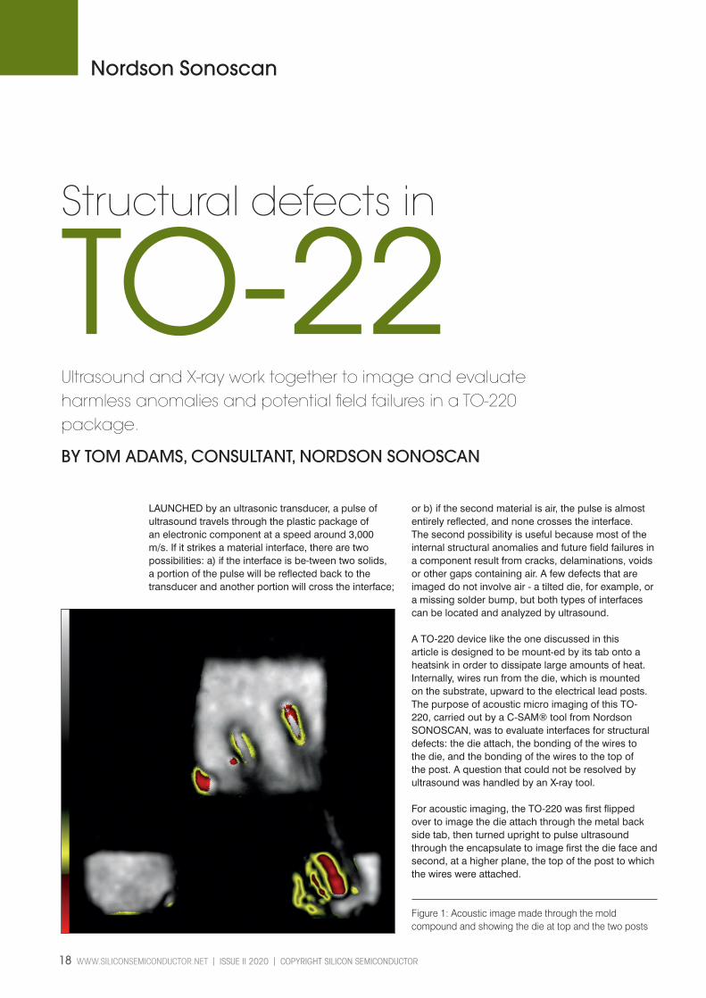
A TO-220 device like the one discussed in this article is designed to be mount-ed by its tab onto a heatsink in order to dissipate large amounts of heat. Internally, wires run from the die, which is mounted on the substrate, upward to the electrical lead posts. The purpose of acoustic micro imaging of this TO-220, carried out by a C-SAM® tool from Nordson SONOSCAN, was to evaluate interfaces for structural defects: the die attach, the bonding of the wires to the die, and the bonding of the wires to the top of the post. A question that could not be resolved by ultrasound was handled by an X-ray tool.
For acoustic imaging, the TO-220 was first flipped over to image the die attach through the metal back side tab, then turned upright to pulse ultrasound through the encapsulate to image first the die face and second, at a higher plane, the top of the post to which the wires were attached.
Figure 1: Acoustic image made through the mold compound and showing the die at top and the two posts
COPYRIGHT SILICON SEMICONDUCTOR l ISSUE II 2020 l WWW.SILICONSEMICONDUCTOR.NET 19
Nordson Sonoscan
At each site, the transducer scanned back and forth a few mm above the area of interest, each second launching thousands of ultrasonic pulses and receiving their return echoes. The echo from each x-y scanned location becomes one pixel in the acoustic image of that area.
From each returning echo the following information is gathered: the echo’s acoustic frequency, its amplitude, its polarity, and the depth from which it was reflected. In these images, the colors report amplitude and polarity.
An acoustic image of all three elements in the package is shown in Figure 1. The vertical distance between the die and the posts is too great to be within the same focus. Figure 1 is therefore made from parts of two acoustic images, one focused on each of the two depths within the package.
The right lead attached to the die at top has a very small red area, but the wire bond area is essentially intact. The red area at the lower left corner of the die, however, is a void that could grow with repeated thermal cycles and cause wire bonds to break. Whether this void is enough to cause rejection of the part de-pends on the application. It might be suitable in a commercial application, but perhaps not in a military application.
The two wires visible on the die clearly run to the post at the right. There is no indication in this view of wires running to the left post. In this case the wire has a very fine diameter and is too small to be resolved at the low ultrasonic frequency needed to penetrate the mold compound. There is, however, a faintly brighter area on the left post that somewhat resembles a bonded wire.
The back side of the die (Figure 2) was imaged through the metal substrate, to which the die is attached. The variously shaped small red features within the area of the die are voids - red here indicates that there is air in the voids. There are no truly dangerous features such as very large delaminations, or voids close to the corners of the die. The voids cover, in total, about four percent of the die area. The TO-220 package is designed to remove large amounts
of heat swiftly, so these relatively small well-spaced voids in the die attach may pose little threat.The problem area in this component, as can be seen in Figure 1, is the right lead post and the wires attached to its top. The red areas are likely voids, but their exact placement and relative danger must be sorted out. To do so, two different imaging modes were used.
The first was a mode that can, during a single scan, image multiple progressively deeper thin slices of the sample being viewed. At each of the thousands or millions of x-y locations in a given image, ultrasound may be reflected from a single interface, or from multiple interfaces at various depths.
To avoid depth confusion, each image is limited to echoes arriving within a specific time that matches a vertical extent within the part. For the right lead post, a total of 6 gates was defined and imaged, each 600 microns in vertical extent. The echoes from each gate became a separate acoustic image.
Figure 2: Die attach, as imaged through the bottom of the package
At each site, the transducer scanned back and forth a few mm above the area of interest, each second launching thousands of ultrasonic pulses and receiving their return echoes. The echo from each x-y scanned location becomes one pixel in the acoustic image of that area
20 WWW.SILICONSEMICONDUCTOR.NET l ISSUE II 2020 l COPYRIGHT SILICON SEMICONDUCTOR
Nordson Sonoscan
Of the six gates, only gates 3 and 4 revealed details of the two wires and their attachment to the post. In gate 3 (Figure 3). the wire at right is faintly visible. It has no anomalies at this depth except for a small void at its termination. The wire at left has a similar tiny void at its termination, but has a larger void along part of its length.
Gate 4 is seen in Figure 4. The wire at right is very faintly visible. The small void near its tip is visible at this depth. The white area at right is the top of the post to which the two wires are attached. The post extends to the left at least as far as the leftmost void, although it is hidden by overlying features for most of this distance. The large red feature at center is a void, and other voids are scattered about. Red in a delamination or void identifies an area that reflects nearly all of the arriving ultrasound. Red is at the very bottom (=strongest negative echo) in the color map at left. Where the side of a feature becomes steeper and reflects ultrasound less directly in the direction of the transducer, red changes to black. Even steeper sides reflect yellow, the next color on the map.
To get an enhanced view of the interior of this device, it was also imaged with the C-SAM’s nondestructive cross-sectioning feature called Q-BAM (Quanti-tative B-scan Analysis Mode). A line was described on the acoustic image of the top of the package through which cross-sectioning would cut through the area of the two wires bonded to the lead post. The resulting acoustic cross-sectional image is the dimensionally accurate equivalent of a physical cross sectioning made by cutting down through the package along the same line.
If the sample were physically sawn open along the same line, the same features would be found in the same locations. A light photograph of the sectioned face would look much like the acoustic cross-section. The concept can also be used in a different manner: before physical sectioning, the sample may be imaged acoustically to spot the location through which the physical section will pro-vide the desired information.
The white horizontal line just below the centre of Figure 5 is the line along which the transducer scanned this component in order to produce the acoustic cross-section in the top portion of the Figure. On its first pass along this line, the transducer accepted echoes only from a defined thin depth at the bottom of the package just above the post. The transducer was then raised very slightly and scanned back along the line. By the time it reached the top of the package it had collected the echoes needed to produce the acoustic cross-section seen in the top section of Figure 5.
In the sectional view, the surface of the package is marked by a horizontal red line. In the bottom half, the cross-sections of five features are shown running from left to right. Each feature lies directly above its location
Figure 3: The two wires attached to the right post. Red areas are anomalies
Figure 4: Same view, but in a slightly deeper gate
COPYRIGHT SILICON SEMICONDUCTOR l ISSUE II 2020 l WWW.SILICONSEMICONDUCTOR.NET 21
Nordson Sonoscan
on the thicker white line in the top view below. From left to right, these features are:
1. a large air gap on the surface of the post.2. the left wire and the void on top of it.3. the large void to the left of the right wire.4. largely the interface between the mold compound and the post.5. a void at the top of the post itself.
There is a sixth, rather small feature, apparently a void, directly above6. #1, just below the package surface.
The acoustic images in Figures 1 through 5, however, do not reveal all the wires extending from the die to the posts. The acoustic images revealed two fairly large wires. Smaller diameter wires would be difficult to see because they scatter most ultrasound away from the transducer. In addition, a smaller diam-eter wire might be invisible acoustically at low frequencies. If ultrasound is entirely blocked by an air interface, the wires beneath the air gap will not be imaged.
Subsequently a Dage Quadra 7 X-ray system was used to image the TO-220. An X-ray beam is not stopped or even attenuated by an air gap. Imaging was first attempted through the heat sink, but the thickness of the metal was too great. (Ultrasound would have penetrated the metal but would still have been scattered rather than reflected by the round wires.) to get additional information. The TO-220 was therefore X-rayed from the side, a longer route through the much less attenuating mold compound. The results are seen in Figure 6.
Four wires are visible as vague dark lines marked by numbers in the X-ray image. The image colors have been inverted to make the wires more visible. Their precise orientation cannot be discerned, but it seems likely, taking into consideration the very faint features on the left post in Figure 1, that two wires run from the die to each of the two posts.
Figure 5: Top portion is a non-destructive cross-section through the horizontal white line below the legend
Fig 6: An X-ray beam inserted into the side of the mold compound revealed the four wires
The acoustic images revealed two fairly large wires. Smaller diameter wires would be difficult to see because they scatter most ultrasound away from the transducer
22 WWW.SILICONSEMICONDUCTOR.NET l ISSUE II 2020 l COPYRIGHT SILICON SEMICONDUCTOR
JST
Ensure wet process cleaning equipment successExpert consultation can keep semiconductor production on track through installation and beyond.
BY JST
FOR SEMICONDUCTOR MANUFACTURERS, compound semiconductor manufacturers, raw wafer material suppliers, and R&D labs, utilizing wet process cleaning equipment is critical to producing extremely reliable products, so partnering with a vendor with deep expertise in all aspects of the process – from equipment selection, design specification, testing, and installation/hook up – can be critical to success.
In such fabrication, “cleaning” refers to the etching process used, which precisely removes thin layers of material. In other applications, cleaning can also refer to the use of agents such as solvents, acids or bases to remove unwanted particulates and other contaminates such as photoresist.
COPYRIGHT SILICON SEMICONDUCTOR l ISSUE II 2020 l WWW.SILICONSEMICONDUCTOR.NET 23
JST
The cleaning process may involve moving product into extremely hot chemical baths of acids, bases, or flammable solvents, so consulting with an expert can improve safety and ergonomics. It often requires selecting the most appropriate options from a number of technologies. This may involve various chemistries, temperature controls, chemical baths/dips, ergonomic designs, as well as cleaning, filtration, ventilation, safety, and disposal technologies.
It may also involve automating/upgrading the cleaning process for high-volume production. If the process takes place in a cleanroom, then the entire system including motors and robotics must be appropriate for that environment.
Hitting any snag can cause quality or safety issues, delay production, or even cost millions if the equipment must be prematurely replaced to accommodate automation. To avoid these “snags”, it can be invaluable to partner with an equipment manufacturer with industry expertise that can help to optimize the entire product life cycle from start to finish.
While all aspects of wet process cleaning are important to consider, failing to plan for even the smallest details of cleaning equipment can lead to challenges like not complying with the local fire or building codes or even being able to get it through doors, hallways or elevators into a clean room.
One area that is often overlooked but can be essential to consider is “facilitization” – meaning the installation, hook up (supplying deionized water, chemistries, drain lines, exhaust system etc.) and safety compliance. Facilitization is a major cost when considering new production equipment and changes in the equipment design to accommodate existing facility constraints can reduce this cost. That is why it is important to work with an equipment supplier that takes the facilitization cost into consideration when quoting a project.
“The facilitization process needs to be thought through because missing important details can cause serious problems that can compromise production and require retrofitting,” says Louise Bertagnolli, president of Boise ID-based JST Manufacturing, which designs and manufactures manual and automated cleaning equipment, including proprietary systems with all the features and transfer devices needed for a complete turnkey cleaning process.
As an example, Bertagnolli points to a variety of logistics that must be properly implemented. This can include, for instance, getting the product and chemistries in and out of the tool, and getting the tool into the cleanroom and set up, not to mention meeting safety and exhaust system requirements, etc.
“Because the cleaning equipment can be relatively large, even the size of elevators, doors and hallways
must be checked to ensure it fits,” she says. “Failing this, one manufacturer had to have a crane lift the equipment through a 6th story window.”
So, to prevent mistakes and ensure that wet process cleaning equipment is designed, installed and “facilitizized” in complete compliance with all safety and performance requirements, it is important for the manufacturer to work with an equipment manufacturer with the expertise to provide one-stop guidance. Getting needed expertise up front ensures that the wet process cleaning equipment will perform as required, with no unwelcome surprises.
Planning for successSpecifying for safety and compliance is critical and many aspects need to be sorted through to ensure the tool is designed to be integrated with the semiconductor manufacturing plant.
In terms of complying with fire codes, Bertagnolli says that if the semiconductor manufacturer has its own fire system in a clean room, then the cleaning equipment needs to communicate with it.So, if the tool has an emergency situation
24 WWW.SILICONSEMICONDUCTOR.NET l ISSUE II 2020 l COPYRIGHT SILICON SEMICONDUCTOR
JST
and needs to shut down due to fire, it must notify the house fire alarm system. Fire suppression lines must also be properly sealed and maintain sufficient pressure. Also, to qualify for fire insurance, factory mutual approved materials must be utilized.
When complying with OSHA, she adds that the manufacturer needs to have a three-foot clearance in front of lockout, tag-out areas when powering down for safety. So, this needs to be planned out as well.
According to Bertagnolli, however, there are a number of areas that are prone to mistakes during facilitization if expert guidance is not readily available. In these areas, she suggests that it is particularly important to seek help from an industry expert that can provide one-stop guidance as needed.
For example, to avoid unplanned problems that can delay production and may require expensive retrofits or workarounds, Bertagnolli says that it is necessary to plan for the logistics of the install, down to which elevators, hallways, and doors the wet processing tank/equipment must fit through.
She adds that because many clean rooms have sub floors, it is also necessary to ensure there are structural support/leg levelers on the right floor location.
For safety compliance and performance, the manufacturer must also provide sufficient exhaust system air flow velocity, at specific cubic feet per minute rate, designed for the production space.
In addition, facilitization involves correctly hooking up to deionized water, chemistries, and drain lines without any leaks.
“A common error is failing to provide pump pressure to chemistry lines when these need to be brought in from afar,” says Bertagnolli. “And per safety codes, dual containment is required on chemical lines.”
The chemical line/tank fill systems, in fact, must be configured correctly, or the chemistries will lack sufficient pressure to properly feed the tool or have other issues such as large amounts of entrapped gas. Facility chemical system’s with chemical lines that take too many turns, becoming convoluted, can reduce pressure to the point where the tank fails to fill. So, the chemical lines must be configured in a more direct manner that maintains enough pressure to properly supply the tool/fill the tank.
“For facilitization to go off without a hitch, a lot of expertise, planning, and attention to detail has to brought to the project beforehand,” says Bertagnolli.According to Bertagnolli, thorough facilitization will even plan for and ease maintenance tasks to avoid unnecessary safety risk or cost.
For example, how a water line runs through the cleanroom should be considered because it can decrease safety and efficiency if it encroaches on the space used to perform maintenance tasks. If planned for, however, the waterline or the cleaning equipment’s maintenance space can be located in different, non-conflicting areas.
The bottom line is that for wet process cleaning equipment to be implemented smoothly and correctly, a lot of details need to be expertly determined in order to effectively handle design specification, facilitization and production.
When well-planned with appropriate one-stop guidance, the whole enterprise can get implemented correctly the first time at minimal cost, with production going smoothly far into the future.
Facility chemical system’s with chemical lines that take too many turns, becoming convoluted, can reduce pressure to the point where the tank fails to fill. So, the chemical lines must be configured in a more direct manner that maintains enough pressure to properly supply the tool/fill the tank
26 WWW.SILICONSEMICONDUCTOR.NET l ISSUE II 2020 l COPYRIGHT SILICON SEMICONDUCTOR
IMEC / Park Systems
Carrier profiling in high vacuum using scanning spreading resistance microscopy and scanning capacitance microscopy
Scanning Spreading Resistance Microscopy (SSRM) and Scanning Capacitance Microscopy (SCM) are both established scanning probe-based methods for two-dimensional carrier profiling. Their initial development was mainly pushed by the microelectronics industry looking for 2D alternatives for their 1D carrier/dopant profiling techniques, such as Capacitance-Voltage (C-V) measurements, Secondary Ion Mass Spectrometry (SIMS), and Scanning Resistance Profiling (SRP).
BY LENNAERT WOUTERS1, ALBERT MINJ1,2, UMBERTO CELANO1, THOMAS HANTSCHEL1, WILFRIED VANDERVORST1,2, KRISTOF PAREDIS1
IN SSRM, the resistance of the current spreading through the nanoscale tip-sample contact is measured while scanning the probe. The key to its large sensitivity and spatial resolution lies in the presence of a pressure induced metallic pocket below the tip apex resulting in a (nearly) ohmic tip sample contact. As a result, the measured resistance is dominated by the spreading resistance and hence dependent on the local sample resistivity ρ:
Rspreading = ρ/4a,
Where a represents the contact size. The main advantages of SSRM include a very high spatial resolution (~ 1 nm) and a large sensitivity and dynamic range (1014-1020 cm-3).
In SCM, small capacitance variations (~10-21 F)
between the tip and the sample are measured using a high frequency capacitance sensor while scanning the probe. Highly doped regions show a low differential capacitance dC/dV, while lowly doped areas exhibit a relatively larger capacitance change. The main advantages are the large dy namic range and the carrier type sensitivity as n- and p-type show opposite phases in their dC/dV signals.
In both methods, it is not straightforward to convert the measured values directly into quantitative values for carriers because detailed information on the probe and sample surface are missing. Hence, a calibration against a known standard is generally the most straightforward way for converting resistance/differential capacitance to resistivity/carrier concentrations.
In fact, both techniques exhibit pros and cons, but are quite complementary; SSRM provides the highest spatial resolution while SCM provides carrier type sensitivity.
1. IMEC, Leuven, Belgium, 2. Department of Physics and Astronomy, University of Leuven, Leuven, Belgium)
IMEC Park v1.indd 26IMEC Park v1.indd 26 02/07/2020 12:4002/07/2020 12:40
COPYRIGHT SILICON SEMICONDUCTOR l ISSUE II 2020 l WWW.SILICONSEMICONDUCTOR.NET 27
IMEC / Park Systems
As current state-of-the-art devices are entering the sub 10 nm nodes, the requirements for materials and device characterization are being pushed to their limits, requiring every aspect of the measurement to be optimized for successful measurements, for instance the probe, the sample preparation, and the measurement environment.
In this application note, we review the performance of the Park NX-Hivac atomic force microscope (AFM) from Park Systems [1] for SSRM and SCM applications, based on the following three samples:
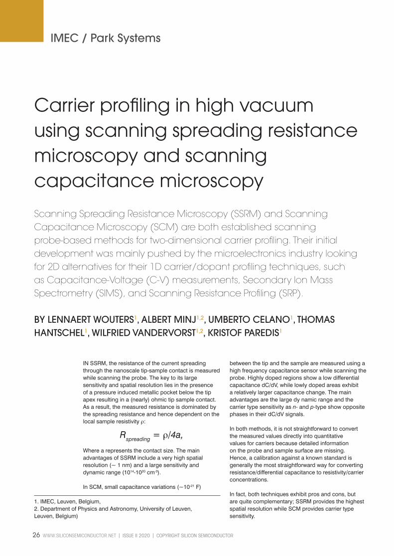
1. A p-type doped silicon calibration sample (imec CS08-SiB): a sample consisting of various Boron doped epitaxial silicon layers (~600 nm) with known doping concentration (Figure 1).
2. An n-type doped silicon calibration sample (imec CS01-SiAs): a sample consisting of various arsenic doped epitaxial silicon layers with known doping concentration (Figure 5). This sample additionally has a p-type doped layer embedded in the stack.
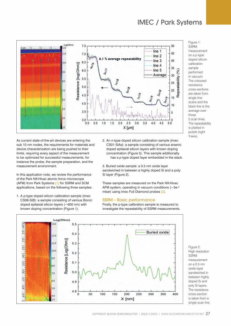
3. Buried oxide sample: a 0.5 nm oxide layer sandwiched in between a highly doped Si and a poly Si layer (Figure 2).
These samples are measured on the Park NX-Hivac AFM system, operating in vacuum conditions (~5e-5 mbar) using imec Full Diamond probes [2].
SSRM – Basic performanceFirstly, the p-type calibration sample is measured to investigate the repeatability of SSRM measurements.
Figure 1: SSRM measurement on a p-type doped silicon calibration sample performed in vacuum. The coloured resistance cross-sections are taken from single line scans and the black line is the average over those 5 scan lines. The repeatability is plotted in purple (right Y-axis).
Figure 2: High resolution SSRM measurement on a 0.5 nm oxide layer sandwiched in between highly doped Si and poly Si layers. The resistance cross-section is taken from a single scan line.
IMEC Park v1.indd 27IMEC Park v1.indd 27 02/07/2020 12:4002/07/2020 12:40
28 WWW.SILICONSEMICONDUCTOR.NET l ISSUE II 2020 l COPYRIGHT SILICON SEMICONDUCTOR
IMEC / Park Systems
Figure 1 shows that excellent repeatability is achieved in SSRM measurements on silicon. Note that the repeatability is better in the highly doped layers. As a reference, for identical scanning parameters, typically a repeatability of 15-20 % is achieved in air highlighting the added value of high vacuum [3].
Secondly, to assess the resolution of SSRM the buried oxide sample is measured. Figure 2 demonstrates that the 0.5 nm oxide layer embedded in silicon can easily be observed in SSRM measurements as an increase in the resistance. The doubling of the resistance on the thin oxide indicates that the electrical contact
radius is similar as the oxide thickness, highlighting a sub-nm resolution [2].
Finally, the p-type calibration sample is measured in air and in vacuum with the same probe to verify the advantages of performing SSRM measurements in a vacuum environment. The results are summarized in Figure3. As expected, in order to obtain an image of similar quality, the applied force to the tip required for a good electrical tip-sample contact had to be increased by almost 50 % when moving from vacuum to ambient environment. This observation suggests that the metallic pocket below the tip apex is induced
Figure 3: SSRM measurements on a p-type doped silicon calibration sample performed in vacuum and in air with the same probe. The resistance cross-sections are the average over 50 scan lines.
Figure 4: SSRM resistance and carrier concentration maps of an n-type doped silicon layer in a solar cell sample.
IMEC Park v1.indd 28IMEC Park v1.indd 28 02/07/2020 12:4002/07/2020 12:40
COPYRIGHT SILICON SEMICONDUCTOR l ISSUE II 2020 l WWW.SILICONSEMICONDUCTOR.NET 29
IMEC / Park Systems
at a lower pressure in vacuum as compared to in air. Therefore, measurements in vacuum environment can be performed with a lower force applied to the tip which will result in less tip wear and thus higher resolution [2].
From the results shown above it can be concluded that the repeatability and resolution of SSRM measurements performed on the Park NX-Hivac AFM are state of the art, and that the vacuum conditions in the chamber are beneficial for conducting repeatable SSRM experiments.
SSRM – Device measurements & calibrationIn general, the calibration samples allow to convert the resistance map of an unknown sample to a carrier
concentration map. To do so, the calibration sample is measured with the same probe and scan parameters as the measurement on the sample of interest. As an example, in Figure 4, the resistance and carrier concentration maps of an n-type doped silicon layer in a solar cell are shown.
The carrier concentration map is calculated from the resistance map by using the calibration curve that is shown in Figure 5. The resistance data points are taken from the average resistance values measured over the 5 layers with known doping levels. The calibration curve is obtained by interpolation of these data points.
It can be concluded that the good measurement repeatability on both the sample and the standard
Figure 5: SSRM measurement on an n-type doped silicon calibration sample. The resistance cross-section is taken from the average of 50 scan lines. The resistance versus dopants data points are taken from the average resistance values measured over the 5 layers with known doping levels in the calibration sample.
Figure 6: SCM dC/dV amplitude and phase measurements on an n-type doped silicon calibration sample.
IMEC Park v1.indd 29IMEC Park v1.indd 29 02/07/2020 12:4002/07/2020 12:40
30 WWW.SILICONSEMICONDUCTOR.NET l ISSUE II 2020 l COPYRIGHT SILICON SEMICONDUCTOR
IMEC / Park Systems
allows for an accurate determination of the active carrier concentration in a sample with unknown carrier levels.
SCMThe n-type doped silicon calibration sample is used to evaluate the performance of SCM on the Park NX-Hivac AFM. This sample has, next to the n-type epitaxial layers, also a p-type doped layer in between the substrate and the n-layers.
Figure 6 shows respectively the dC/dV amplitude and the dC/dV phase map obtained from an SCM measurement on the n-type calibration sample. From the phase map, one can clearly distinguish the n and p-layers.
The various n-type layers with different doping concentrations show also a clear contrast in the dC/dV amplitude map. These results demonstrate the carrier concentration sensitivity and the carrier type sensing capability of SCM, even though the spatial resolution is not as good as in SSRM.
The dC/dVamplitude cross-sectionis taken from the average of 50 scan lines. Besides Si, another interesting application of SCM is on III-V material stacks. In Figure 7 the results of an SCM measurement on a doped InGaAs stack are shown and they allow to extract information about the carrier concentration and the carrier type.
ConclusionsThis study shows that scanning spreading resistance microscopy (SSRM) and the scanning capacitance microscopy (SCM) can meet the challenges of carrier profiling the state-of-the-art devices entering the sub 10 nm nodes given the right microscopy tool. This investigation found that Park NX-Hivac is the powerful tool that meets the challenges of ever shrinking devices with its implementation of electrical SPM modes, including SSRM and SCM, in a high vacuum environment. Furthermore, we conclude that the use of Park NX-Hivac vacuum aids significantly to reduce the noise, resulting in an average repeatability of 6.1 % for SSRM measurements.
References
[1] Park NX-Hivac, Retrieved from https://parksystems.com/products/small-sample-afm/park-nx-hivac?highli ght=WyJueC1oaXZhYyIsIm54LWhpdmFjJ3MiXQ==
[2] Hantschel, T., et al. Diamond scanning probes with sub-nanometer resolution for advanced nanoelectronics device characterization, Microelectronic Engineering 159, 46-50 (2016).
[3] Eyben, P. et al. Fundamentals of Picoscience, Subnanometer Characterization of Nanoelectronic devices. Edited by Sattler, K.D., CRC Press (2014)
Figure 7: SCM measurement on a doped InGaAs stack. The dC/dV amplitude and phase cross-sections are taken from the average of 100 scan lines.
IMEC Park v1.indd 30IMEC Park v1.indd 30 02/07/2020 12:4002/07/2020 12:40
PROCESS APPLICATIONS with our BATCHSPRAY® systems: CLEAN RESIST STRIPETCH
Siconnex BATCHSPRAY® Technology.Our innovative BATCHSPRAY® technology is based on a closed system, in which wet chemical cleaning and etching processes are performed highly efficiently. Various chemical processes, including rinsing and drying, are performed fully automatically in a process chamber.
ADVANTAGES■ Automated dry-in, dry-out process■ High throughput, due to 25 or 50 wafer chamber■ Small footprint (~ 25 sqft)■ For 2” to 12” substrates■ Manual or automated robot loading with the pa-
tented Retainer Comb Handling (RCH) System (FOUP, SMIF, etc. compatible)
SiTimes makes a case for MEMS oscillators versus quartz-crystal–based clocking sources.
BY JEHANGIR PARVERESHI, SR. MANAGER, CUSTOMER ENGINEERING AND HARPREET CHOHAN, DIRECTOR, MARKETING
THE EXPLOSIVE GROWTH in internet-connected devices, or the internet of things (IoT), is driven by the convergence of people, devices and data across the web. Future growth will be strongly influenced by wearable technology as products transition from the laptop to the pocket to the body. Activity trackers are leading this segment in the number of units shipped per year, followed by smart watches and medical monitors/devices, as well as wearable cameras and smart glasses. These devices are enabled by advancements in MEMS and sensor technology, wireless connectivity and new power savings capability.
Wearable devices leverage new timing technologyAll electronic products require one or more timing devices depending on the processor, partitioning, and various functions in the system. Traditionally,
32.768-kHz crystals and low-power MHz quartz-based oscillators have been used for implementing clock functions in battery-powered electronic systems. A new class of ultra-low-power, low-frequency MEMS oscillators now offers advantages over the ubiquitous 32-kHz crystal clock. Innovations in MEMS timing technology is making significant impact in IoT and wearables, especially in the areas of size and power savings.
Key benefits of MEMS timing solutions for IoT and wearables include: Smaller footprint – 80% smaller than quartzSmallest 32-kHz oscillator in a 1.5 × 0.8-mm chip-scale package (CSP) Oscillator output drives multiple loads, reducing component count and board area Better stability, as good as 3 ppm – translates to higher savings
Figure 1: Package size and pin location of 32 kHz MEMS XO and TCXO compared to quartz XTALs.
SI Times v1.indd 32SI Times v1.indd 32 02/07/2020 12:4202/07/2020 12:42
COPYRIGHT SILICON SEMICONDUCTOR l ISSUE II 2020 l WWW.SILICONSEMICONDUCTOR.NET 33
SI Times
MEMS XO (oscillator) is 2× to 3× more accurate compared to quartz MEMS TCXO (temperature compensated oscillator) is 30× to 40× more accurate Better stability means less reliance on network timekeeping updates, longer sleep-mode periods, and 30% to 50% lower power compared to quartz XTAL + SoC oscillator Programmable frequency from 1 Hz to 2.5 MHz for sensor interface – enables new architectural options More resilient – 50× greater resistance to shock and vibration
All-silicon MEMS timing solutionsUnlike quartz-based devices, silicon MEMS oscillators employ modern packaging technologies. MEMS oscillators consist of a MEMS resonator die mounted on top of a high-performance, programmable analog oscillator IC that is molded into standard low-cost plastic SMD packages, with footprints compatible with quartz devices. To support the space requirements of ultra-small applications, SiTime MEMS oscillators are available in ultra-small CSPs. MEMS oscillators are based on a programmable architecture that allows customization of features including frequency, supply voltage, output swing, and other features.
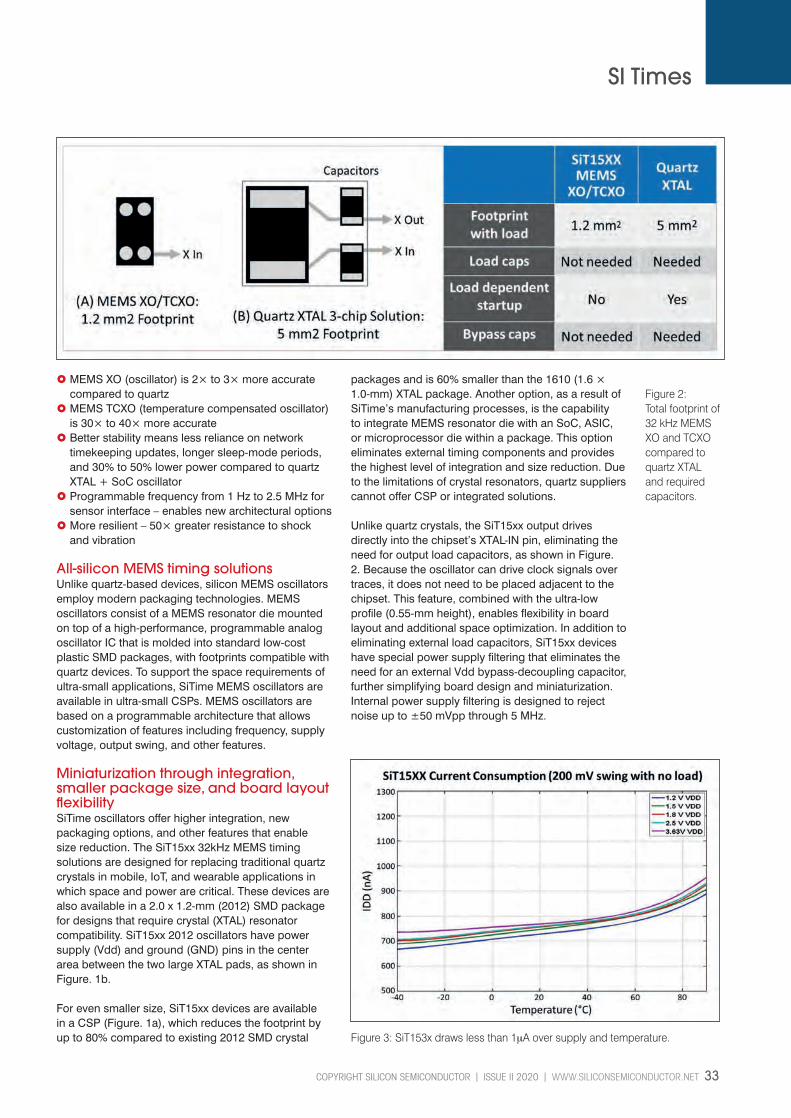
Miniaturization through integration, smaller package size, and board layout flexibilitySiTime oscillators offer higher integration, new packaging options, and other features that enable size reduction. The SiT15xx 32kHz MEMS timing solutions are designed for replacing traditional quartz crystals in mobile, IoT, and wearable applications in which space and power are critical. These devices are also available in a 2.0 x 1.2-mm (2012) SMD package for designs that require crystal (XTAL) resonator compatibility. SiT15xx 2012 oscillators have power supply (Vdd) and ground (GND) pins in the center area between the two large XTAL pads, as shown in Figure. 1b.
For even smaller size, SiT15xx devices are available in a CSP (Figure. 1a), which reduces the footprint by up to 80% compared to existing 2012 SMD crystal
packages and is 60% smaller than the 1610 (1.6 × 1.0-mm) XTAL package. Another option, as a result of SiTime’s manufacturing processes, is the capability to integrate MEMS resonator die with an SoC, ASIC, or microprocessor die within a package. This option eliminates external timing components and provides the highest level of integration and size reduction. Due to the limitations of crystal resonators, quartz suppliers cannot offer CSP or integrated solutions.
Unlike quartz crystals, the SiT15xx output drives directly into the chipset’s XTAL-IN pin, eliminating the need for output load capacitors, as shown in Figure. 2. Because the oscillator can drive clock signals over traces, it does not need to be placed adjacent to the chipset. This feature, combined with the ultra-low profile (0.55-mm height), enables flexibility in board layout and additional space optimization. In addition to eliminating external load capacitors, SiT15xx devices have special power supply filtering that eliminates the need for an external Vdd bypass-decoupling capacitor, further simplifying board design and miniaturization. Internal power supply filtering is designed to reject noise up to ±50 mVpp through 5 MHz.
Figure 2: Total footprint of 32 kHz MEMS XO and TCXO compared to quartz XTAL and required capacitors.
Figure 3: SiT153x draws less than 1µA over supply and temperature.
SI Times v1.indd 33SI Times v1.indd 33 02/07/2020 12:4202/07/2020 12:42
34 WWW.SILICONSEMICONDUCTOR.NET l ISSUE II 2020 l COPYRIGHT SILICON SEMICONDUCTOR
SI Times
Extended battery life through low current consumptionLow frequency, low power 32-kHz timekeeping devices are widely used in mobile devices where the device is continuously ON for time keeping or controlling sleep modes. These low frequency oscillators are also used to time events such as monitoring and control functions in a power management IC (PMIC) used in battery-powered devices or to perform short system wakeup for timing reference synchronization.
Traditionally, systems generate the 32-kHz clock signal by connecting a tuning fork type or AT-cut quartz crystal to an on-chip pierce oscillator circuit. These quartz time-keeping oscillators are always ON and continuously drawing a few microamps. SiTime’s SiT15xx 32-kHz MEMS oscillators draw less than a microamp of current and can run off a range of regulated or unregulated supply voltages, from 1.2 to 3.63 V. Figure. 3 plots a SiT153x oscillator drawing less than 1-µA oversupply and temperature.
Measured frequency stability32-kHz MEMS timing devices have a temperature coefficient that is extremely flat across temperature compared to quartz crystals as shown in Figure. 4. The SiT15xx oscillators are calibrated (trimmed) to guarantee frequency stability to less than 10 ppm at room temperature and less than 100 ppm over the full –40°C to 85°C temperature range. In contrast, quartz crystals have a classic tuning fork parabola temperature curve with a 25°C turnover point as indicated by the red lines in Figure. 4.
Figure. 5 plots the frequency stability of 32-kHz MEMS TCXOs. In these devices, the temperature coefficient is calibrated and corrected over temperature with an active temperature correction circuit. The result is a 32-kHz TCXO with less than 5-ppm frequency variation over temperature. This low level of frequency variation results in extremely accurate clocks that translate to significant power savings. With higher accuracy, wireless systems are less reliant on network
Figure 4: SiT1532 MEMS XO frequency stability compared to quartz XTAL –160 to –200 ppm over temp.
Figure 5: SiT1552 MEMS TCXO frequency stability is 30 to 40 times more accurate than quartz XTAL.
Figure 6: Early ON time (or window widening) is affected by clock accuracy and causes a power penalty.
SI Times v1.indd 34SI Times v1.indd 34 02/07/2020 12:4202/07/2020 12:42
COPYRIGHT SILICON SEMICONDUCTOR l ISSUE II 2020 l WWW.SILICONSEMICONDUCTOR.NET 35
SI Times
timekeeping updates and can stay in sleep mode for much longer periods of time.
Extended battery life through better frequency stabilityFrequency stability, the clock’s stability over voltage and temperature, translates to power conservation. Many mobile and IoT devices reduce power consumption by shutting down the functional blocks with the highest current drain when inactive. However, the system must wake up and periodically communicate with the network. Higher frequency stability allows the device to stay in its low-power state, or sleep state, for longer periods, resulting in significant power savings.
Many wearables continuously collect data and compress and upload it to the cloud via an internet hub device such as a smartphone. This upload is
transferred in short bursts that last a few milliseconds and then the device goes to sleep to conserve power. The cyclic sleep scenario is typical of battery-powered devices in which the device core is shut down for a pre-set time called “sleep time,” typically in the range of two to 10 seconds, and awoken when it needs to transmit data during a short burst. The connection event is the “ON” time during which certain functional blocks of the device wake up and stay active for short periods.
Power consumption is proportional to the ratio of “ON” time to the time that devices spend in the “sleep” state. And the sleep clock accuracy (SCA) of the 32-kHz clock that is used to time the sleep state has a direct impact on the battery life. Sleep clock inaccuracies cause the radio receiver (RX) to turn on earlier and stay on longer to avoid missing packets
The table shows that tighter slave clock accuracy reduces early ON time, thereby reducing power consumption.
Figure 7: Power savings through use of MEMS TCXO compared to quartz XTAL resonator.
SI Times v1.indd 35SI Times v1.indd 35 02/07/2020 12:4202/07/2020 12:42
36 WWW.SILICONSEMICONDUCTOR.NET l ISSUE II 2020 l COPYRIGHT SILICON SEMICONDUCTOR
SI Times
from the master. Clock inaccuracy, measured in ppm, extends early ON time (ΔT), as shown in Figure. 6: ΔT = (SCA) × (SLEEP TIME).
MEMS-based TCXOs, such as the SiT1552, with less than 5-ppm frequency variation over temperature, is a much more accurate alternative than quartz crystals. This accuracy reduces early ON time and allows the system to stay in sleep mode longer. Using a SiT1552, system designers can leverage compression and transmit data in short bursts only when required while keeping the device in its lowest-power sleep state for extended periods and potentially achieve up to twice the battery life.
Figure. 7 shows 30% power savings gained through using a 5-ppm 32-kHz TCXO compared to a 200-ppm 32-kHz quartz-crystal resonator. Shown are two plots of the average current consumption over 1 connection interval for various sleep times ranging from 2 seconds to 20 seconds. These per-cycle average values are computed from a BLE SoC sleep current of 1.8 µA, a radio receiver power of 9.3 mA, a transmit power of 9 mA, and an average ON-time base-band processing current of around 5 mA.
Extended battery life with programmable featuresThe analog oscillator IC in SiT15xx devices supports several functions, including a low noise sustaining
circuit, an ultra-low-power precision PLL, and an ultra-low-power programmable output driver. The fractional-N PLL with sub-hertz resolution is used for device calibration and frequency programming from 2.5 MHz down to 1 Hz. The capability to lower output frequency significantly reduces current consumption. Quartz XTALs, due to the physical size limitations of the resonator at low frequencies, do not offer frequencies lower than 32.768 kHz. With lower-frequency options, the SiT15xx family enables new architecture possibilities in battery-powered applications in which the reference clock is always running
Unlike standard oscillators, SiT15xx oscillators can function in tandem with the on-chip 32-kHz oscillator circuit via the oscillator’s highly programmable output driver. The output driver can generate various common-mode voltages and swing levels to match different implementations of the on-chip 32-kHz oscillator circuits, as shown in Figure. 8. This output swing is factory-programmable from full swing down to 200 mVpp for the lowest power. The ability to reduce output frequency and output driver current significantly reduces the output load current (C × V × F). See SiT15xx datasheets for load calculation details and examples at https://www.sitime.com/products/khz-oscillators and https://www.sitime.com/products/mpower-oscillators-1-hz-26-mhz
Figure 8: Unique NanoDrive output swing is programmable down to 200 mV to minimize power.
Figure 9: Typical wearable timing architecture.
SI Times v1.indd 36SI Times v1.indd 36 02/07/2020 12:4202/07/2020 12:42
1000STANDARDS& COUNTINGSEMI
Industry counts on SEMI standards.SEMI is the global industry association serving the product design and manufacturing chain for the electronics industry.
Check out our new standards on SMT & PCB Manufacturing Equipment Communication, Panel Level Packaging & Energetic Materials at:
38 WWW.SILICONSEMICONDUCTOR.NET l ISSUE II 2020 l COPYRIGHT SILICON SEMICONDUCTOR
SI Times
MEMS are 50 times more robustBy nature of their application, IoT and wearables are used in a variety of environments and can be subjected to frequent and extreme mechanical shock and vibration. When operating in harsh environments, quartz oscillators will degrade and not conform to datasheet specifications. Some quartz oscillators are especially sensitive to sinusoidal vibration and shock and will exhibit significant frequency variation. The SiT15xx device architecture lends itself to higher reliability and resiliency to harsh environmental factors relative to their quartz counterparts. The very small mass (1,000 times smaller than quartz resonators) and structural design of SiTime resonators make them extremely immune to external forces such as vibration and shock. For more details on the resiliency and reliability of MEMS oscillators, see technology paper at: https://www.sitime.com/sites/default/files/gated/AN10045-SiTime-Resilience-Reliability-MEMS-Oscillators_0.pdf
Application and design examplesIn the wearable market, products are increasing in functionality while, at the same time, they must consume less power and space. 32-kHz MEMS timing
solutions can be used for true pulse-per-second (pps) timekeeping, RTC reference clocking, and battery management timekeeping to lengthen battery life and shrink footprint.
Figure. 9 shows the clocking needs in a typical wearable device. A low power 32-bit MCU runs off of a 16-MHz crystal to clock the core and peripherals, and a 32-kHz crystal is used for real-time clocking. The MCU sends data to a connectivity chip that runs off of a 32-kHz crystal used for sleep clock timing.
Figure. 10 illustrates a design in which a programmable 1-Hz to 32-kHz SiT1534 MEMS oscillator is used for the sensor application and a 32-kHz MEMS SiT1532 reference clock drives the RTC in an MCU. In this design, the board space is reduced to less than half through use of 1.5 × 0.8-mm CSP oscillators.
Figure. 11 shows an architecture in which a 32-kHz timing solution is required for two chips: a reference clock for the microcontroller and the sleep clock for the Bluetooth chip. In this design, a single MEMS timing device in a tiny 1.5 × 0.8-mm CSP, drives two loads and replaces two 32-kHz quartz XTALs. The footprint is eight times smaller than a design that uses two quartz XTALs in 2012 SMD packages plus the four required load capacitors. This design also saves significant power with 100-times-better stability of an SiT1552 TCXO compared to the BLE chip’s internal 32-kHz RC over temperature.
SummaryInnovation in the rapidly growing wearable and IoT segments is fueled by advancements in underlying technologies. MEMS timing technology is one of the key supporting technologies enabling the trend toward smaller size, lower power, and increased robustness.MEMS timing reduces footprint through: Smaller, unique packages Higher integration that reduces component count Board layout flexibility
MEMS timing reduces power consumption through: Lower core current draw Higher frequency stability that enables longer sleep states Programmable frequency Programmable output swing voltage
MEMS timing increases robustness through: Greater resistance to shock and vibration error MEMS XOs/TCXOs offer an alternative to the bulkier, less-accurate quartz-crystal clock sources used in past designs. As the IoT continues to expand with increasingly smaller battery-powered devices, low-frequency MEMS-based devices will provide the optimal timing solution and enable new products that were not previously possible.
Figure 10: Fitness device timing shown in example 1.
Figure 11: Figure.Fitness device timing shown in example 2.
SI Times v1.indd 38SI Times v1.indd 38 02/07/2020 12:4202/07/2020 12:42
www.sensorsinternational.net
3 events 2 days 1 ticket17-18 November 2020Sheraton Brussels Airport Hotel, Belgium
One ticket gives you access to a 2 day event which will see 3 groups of device makers gathered under one roof. Hear over 100 presentations covering the entire spectrum of the compound semiconductor, integrated photonics photonics and global sensor supply chain.
Connecting, informing and inspiring the compound semiconductor industry
www.csinternational.net
Creating and strengthening links between chipmakers and network builders
REGISTER NOW, AND SECURE YOUR PLACE. REGISTRATION ALLOWS ACCESS TO:CS INTERNATIONAL, PIC INTERNATIONAL AND SSI INTERNATIONAL
Sensor Solutions: Market opportunities
www.picinternational.net
Talk to us about sponsorship NOW as it will be another sellout
CS PIC SSI 321 2020 Conf Ad 210 x 297 v3.indd 1CS PIC SSI 321 2020 Conf Ad 210 x 297 v3.indd 1 28/05/2020 13:0228/05/2020 13:02
40 WWW.SILICONSEMICONDUCTOR.NET l ISSUE II 2020 l COPYRIGHT SILICON SEMICONDUCTOR
Camline
Dark Data: Uncovering the path to accelerating R&D programmes
At a time when Baby Boomers are retiring in record numbers, companies are discovering that when seasoned employees leave, they frequently take information with them that could speed future R&D programmes while avoiding unnecessary experimentation. It’s called ‘Dark Data’ and recovering it can be the fastest route for reducing time-to-market, cutting costs and accelerating innovation.
BY DR. DIRK ORTLOFF, CAMLINE
IN TIMES of growing international competition and shrinking market niches, innovating via new or improved products becomes key to success or even to survival. When developing a new product or a new iteration of an existing product, it’s vital to use information from a variety of sources to help shape the process and ensure success.
That said, access to historical information, knowledge and wisdom is also vital to ensure that any new project learns and moves on from those completed beforehand. Experiences gained from existing tactics, previous R&D, scientific papers and old lab books provide the major contribution to the successful realisation of new manufacturing processes and
products. Lessons can be learned, insights can be applied to new projects and even failures or mistakes can be vital in terms of determining how not to approach an issue in a future project.
Building an information-driven R&D function For manufacturers, access to historical information, knowledge and wisdom is the crucial factor in ensuring process and quality control throughout the Research and Development (R&D) function. In diverse high-tech industries such as semiconductors, MEMS and nanomaterials, the experiences and information gained from previous projects provide essential insight when planning and executing a new development.
Dark Data v1.indd 40Dark Data v1.indd 40 02/07/2020 12:4202/07/2020 12:42
COPYRIGHT SILICON SEMICONDUCTOR l ISSUE II 2020 l WWW.SILICONSEMICONDUCTOR.NET 41
Camline
The advent of Industry 4.0 has also introduced the concept of a Digital Twin: a virtual version of a machine, a process or a product, which is composed of the data that they generate. Together with a model of how the real object operates, interacts and evolves, a digital twin can be of enormous help in making informed decisions. With machines, for example, this can provide invaluable context for how machines operate at their most efficient, helping to roadmap the decisions needed to reach a certain objective.
However, too often these different types of data are not being recorded, shared or used – which has given rise to the term ‘dark data.’ Significant amounts of information are either ignored, not saved in the correct location or format, or simply not captured in the first place. Asides from being a waste of valuable time and resource, not looking at or learning from this data can have a serious impact on the efficiency of a business, and in particular, its manufacturing and R&D operations.
The emergence of ‘dark data’ The reliability and accessibility of dark data sources is not ever guaranteed. Colleagues can move on and not leave complete records, meaning it’s not always clear which experiments have been carried out and what the results and findings were. Lab books are a great resource for historical data, but are often only useful to those who wrote them. In terms of computer files, they can be distributed over several file servers, desktops and laptops. Every engineer has their own way of saving and storing information, so various software is used and there is often no consistency in the way data is stored. This leads to a build-up of dark data and in turn, a lack of knowledge.
Studies show that in manufacturing R&D activities, approximately 40% of experiments are repeated. Experts in semiconductor process development estimate that 10-15% of failed and double experiments could be avoided if previous results were more easily accessible. Furthermore, when engineers move from one project to another, there is a risk that experiments can be jeopardised as a new engineer arrives to be greeted with a flood of unstructured and unfamiliar data. When documenting experiment data in R&D projects, the focus should always be on collaborative knowledge management, enabling multi-user access and clear search criteria. However, this can cause problems, as data can be structured (tables, numbers, units) or unstructured (images, emails, documents) and studies have found that up to 80% of a firm’s digitised data is unstructured. Even structured data
may change hourly or daily, and if old or out of date information is not deleted, archived or correctly labelled, inconsistencies and confusions can arise. Searching data can also be problematic, as search criteria and reporting can change project to project and even within one project, depending on the task in question. Added to this, full text search is often not enough to pinpoint the exact data needed. It also doesn’t give the context of the data, such as how the results were achieved, where else the same material or conditions were used, or how a certain component was produced.
This build-up of dark data leads to the undesirable result that certain information is only used within the live cycle of one component or project. This limits the learning for future projects, as only those who were involved in the project or those entering the data themselves can either access it or understand its context.
Solving the dark data issue Despite these challenges, there are strategies and processes that can be put in place by manufacturers to capitalise on dark data and realise significant efficiencies in how they work on new R&D projects. The IT and technology we have access to now allows for sophisticated and intelligent systems of recording, accessing and sorting data, so these problems can be easily overcome.
On one hand, the fact that we can store more data than ever before is a big positive. However, as the amount we can store increases by around 50% every year, there is a risk that we can drown in that data if it is not correctly categorized and recorded in a way that makes it useful for future projects. The solution is to find a more intelligent approach to documenting and managing data, establishing a framework for collaborative learning which is geared towards R&D priorities and delivers faster, cheaper and more efficient routes to market.
In order for the data to work well for R&D, any system must be able to store both structured and unstructured data; manage the relations between all the data and give every entry and link a specific description with explicit meaning. In many ways, this makes it similar to a ‘Single Source of Truth’ solution in that it enables you to manage all of your data in one place.
The system must provide an audit trail which details what changes were made, when and why, and
The solution is to find a more intelligent approach to documenting and managing data, establishing a framework for collaborative learning which is geared towards R&D priorities and delivers faster, cheaper and more efficient routes to market
Dark Data v1.indd 41Dark Data v1.indd 41 02/07/2020 12:4202/07/2020 12:42
42 WWW.SILICONSEMICONDUCTOR.NET l ISSUE II 2020 l COPYRIGHT SILICON SEMICONDUCTOR
Camline
whether they apply to the structured or unstructured data. It must also cater for multi-disciplined working environments, e.g. providing the electrical engineer with electrical test data and the mechanical engineer with stress test data. One of the key considerations when finding an R&D data solution is the format. Usually, R&D data is accumulated and stored in the following ways: Semi-structured data in spreadsheets, text and CSV files (commonly MS Excel): data can be easily imported and exported through a variety of software packages and many manufacturing machines export their data in Excel or CSV format. File-based result data from diverse metrology tools: this is for digital experiment data images, analysis results and diagrams. Context can be easily lost here as the relations between data points are complex and not compatible with search functions on many systems. Existing lab databases: Collecting data from all experiments for traceability purposes; highly valuable in terms of optimising manufacturing operations and providing R&D insight.
PDES: a modern solution Although all of these formats work in their own way, there are limitations on their value to the R&D process unless they are joined up and connected so the data can be contextualised and analysed properly. By
using Process Development Execution System (PDES) software, these existing data silos can be integrated and merged (in one place or virtually linked together) to create a more usable and insightful set of historical information that can be applied to future projects.
The camLine XperiDesk software is an example of PDES implementation, which streamlines R&D activities by collecting data, tracking it through its lifecycle and organising into usable activity blocks. Data from existing silos can be integrated by copying or linking into the software, delivering historical insight which can inform and improve the performance of the current project.
Tools within the software allow users to load and link data from various sources, manage it in its full context and retrieve it as actionable information, thereby providing a full circle approach to the data management process. As technologies continue to evolve and manufacturing capabilities continue to increase, it’s vital that data from historical experiments is not only collected, but used in a way which enhances future innovations without wasting time or resources. PDES is a huge step forward in overcoming the issues caused by the dark data phenomenon and providing engineers with workable, reliable data from multiple sources which can help them achieve greater efficiencies in their work.
SUBMIT YOUR LAB & FAB ARTICLE
www.siliconsemiconductor.net
Research is the foundation for the growth of the Silicon Semiconductor industry.
If you want to highlight the important breakthroughs that you make, submit your latest research stories to: [email protected] It is imperative that Silicon Semiconductor remains a timely resource for this industry, so we are only interested in highlighting very recent work reported in academic papers.
Therefore, please only consider writing a short piece highlighting your work if you have a journal paper that has been accepted and about to appear in press, or a paper that has been published within the last month.
Dark Data v1.indd 42Dark Data v1.indd 42 02/07/2020 12:4202/07/2020 12:42
For more information contact: Jackie Cannon T: 01923 690205 E: [email protected] W: www.angelwebinar.co.uk6 Bow Court, Burnsall Road, Coventry, CV5 6SP. UK T: +44(0)2476 718 970 E: [email protected] W: www.angelbc.com
Expertise: Moderators, Markets, 30 Years + PedigreeReach: Specialist vertical databasesBranding: Message delivery to high level influencers via various in house established magazines, web sites, events and social media
Specialists with 30 year+ pedigree and in-depth knowledge in these overlapping sectors:
Semiconductor (Silicon/Compound) Publications include: Compound Semiconductor, Silicon Semiconductor, CS China, SiS China Power ElectronicsPublications include: Power Electronics World
Future MobilityPublications include: TaaS Technology, TaaS News
Data CentresPublications include: DCS Europe, DCS UK, SNS International
SmartSolar UK & Ireland Publications include: Solar and Power Management, Solar UK and Ireland
Sensors Publications include: Sensor Solutions Magazine,Sensor Solutions International
DigitalisationPublications include: Digitalisation World, Information Security Solutions, Managed Services
MARK ANDREWSMark Andrews is technical editor of Silicon Semiconductor, PIC Magazine, Solar+Power Management, and Power Electronics World. His experience focuses on RF and
photonic solutions for infrastructure, mobile device, aerospace, aviation and defence industries
PHIL ALSOPJournalist and editor in the business to business publishing sector for more than 30 years currently focusing on intelligent automation, DevOps, Big Data and analytics,
alongside the IT staples of computing, networks and storage
JACKIE CANNONDirector of Solar/IC Publishing, with over 15 years experience of Solar, Silicon and Power Electronics, Jackie can help moderate your webinar, field questions and make
the overal experience very professional
DR RICHARD STEVENSONDr Richard Stevenson is a seasoned science and technology journalist with valuable experience in industry and academia. For almost a decade, he has been the editor of Compound
Semiconductor magazine, as well as the programme manager for the CS International Conference
Expert ModeratorsDedicated technical and time-served experts/editors
Webinar Ad NEW 2020.indd 2Webinar Ad NEW 2020.indd 2 22/04/2020 09:5222/04/2020 09:52
44 WWW.SILICONSEMICONDUCTOR.NET l ISSUE II 2020 l COPYRIGHT SILICON SEMICONDUCTOR
PVA TePla Analytical Systems
Rely on SAM for 3D package device analysis
The emergence of highly accurate wafer bonding and die stacking has enabled new generations of 3D semiconductors. As stacks grow, so does complexity, which in turn makes reliable, non-destructive inspection and testing critical to high yield and product reliability. PVA TePla Analytical Systems discusses scanning acoustic microscopy (SAM) as a means to ensure scalable, accurate inspection.
THE CONCEPT BEHIND advanced 3D packaging is to vertically stack multiple dies or wafers – the Z-dimension – to achieve better performance with lower power requirements, smaller size and lower cost. However, as 3D packages become increasingly complex, so do the challenges of identifying defects in multiple layers of stacked dies, silicon interposers and interconnections including through-silicon vias (TSVs) as well as fine-pitch micro-bumps.
With less accessibility to internal components and a need to scan multiple, stacked layers, the focus is now shifting to methods of non-destructive testing both in manufacturing and for failure analysis. Non-destructive testing of 3D packages with scanning acoustic microscopes (SAM) identifies defects down to the sub-micron level for 100 percent inspection and failure analysis.
3D advanced packagingIn general, the term 3D packaging applies to products manufactured by stacking (and bonding) silicon wafers or dies and interconnecting them vertically. This covers many integration schemes, including 3D wafer-level packaging, system in package (SiP), package on package (PoP), 2.5D and 3D, stacked ICs and other forms of heterogeneous integration.
To achieve vertical stacking, early 3D packages relied on interconnects such as wire bonding and flip chips. Today, communication between chips often involves a
silicon or organic interposer or bridge, with TSVs. The interposer acts as the bridge between the chips and the board, while increasing the I/Os and bandwidth.
The concept of utilizing chiplets in 3D designs is also gaining momentum for advanced packaging. In this approach, modular chips – or chiplets – from third party vendors are used to build a package or system by stacking the components vertically.
A key benefit of utilizing chiplets to construct a microelectronic system is the ability to select optimized CPU, IO, FPGA, RF or GPU components. Chiplets can be mixed-and-matched using a die-to-die interconnect scheme involving a silicon interposer, a silicon bridge or high-density fan-out. This approach has been embraced by Intel, which recently announced its new Foveros 3D packaging technology that allows complex, heterogenous logic chips to be stacked directly on top of each other. Intel uses an active interposer instead of a typical passive silicon interposer. As an alternative, Intel is also offering its silicon bridge technology called Embedded Multi-die Interconnect Bridge (EMIB).
The Defense Advanced Research Projects Agency (DARPA), an agency of the US Department of Defense, already plans to develop a large catalog of third-party chiplets for commercial, military and aerospace applications. The goal of DARPA’s CHIPS program (Common Heterogeneous Integration and Intellectual
COPYRIGHT SILICON SEMICONDUCTOR l ISSUE II 2020 l WWW.SILICONSEMICONDUCTOR.NET 45
PVA TePla Analytical Systems
Property Reuse Strategies) is to increase overall system flexibility and reduce design time by as much as 70 percent, according to the agency.
“The vision of CHIPS is an ecosystem of discrete modular, reusable IP blocks, which can be assembled into a system using existing and emerging integration technologies,” writes Andreas Olofsson in program information available from DARPA.
Whether for commercial, consumer or defense-grade components, there are challenges to making the chiplet concept work, including how to verify and test the individual chiplets from a variety of third-party vendors. Integrating multiple chiplets into stacked, 3D packages also requires high-density interconnections, all of which are potential sources of failure.
In comparison to other 3D package types, for example, stacked dies with through-silicon vias (TSV) require much smaller, finer pitch solder bumps that create additional challenges in defect detection. Any defective chiplets in the package will result in a non-functional device even if all other modules are functional.
Given the combined value of the chiplets, interposer and other components, a single defective chiplet or poor interconnection can render the entire 3D package non-functional. This is driving the requirement for 100 percent inspection during manufacturing, ideally with non-destructive testing methods.
Non-destructive testing of 3D packagesManufacturers taking designs into the third dimension face a number of challenges including the need to perform 100 percent inspection with relatively high throughput to identify and remove 3D packages or components that do not meet quality requirements.
Among the available non-destructive methods, scanning acoustic microscopy is the most widely used techniques for testing and failure analysis involving stacked dies or wafers.
SAM utilizes ultrasound waves to non-destructively examine internal structures, interfaces and surfaces of opaque substrates. The resulting acoustic signatures can be constructed into three dimensional images that are analyzed to detect and characterize device flaws such as cracks, delamination, inclusions and voids in bonding interfaces, as well as to evaluate soldering and other interface connections.
A unique characteristic of acoustic microscopy is its ability to image the interaction of acoustic waves with
the elastic properties of a specimen. In this way the microscope is used to image the interior of an opaque material.
Scanning acoustic microscopy works by directing focused sound from a transducer at a small point on a target object. The sound, hitting a defect, inhomogeneity or a boundary inside material, is partly scattered and will be detected. The transducer transforms the reflected sound waves into electromagnetic pulses that are displayed as pixels with defined gray values thereby creating an image.
To produce an image, samples are scanned point by point and line by line. Scanning modes range from single layer views to tray scans and cross-sections. Multi-layer scans can include up to 50 independent layers. Images from different depths can be combined into a single scan as well, called Tomographic Acoustic Micro Imaging (TAMI).
When higher throughput is required, up to 4 transducers can simultaneously scan for defects. Multiple transducers can be used on a single
46 WWW.SILICONSEMICONDUCTOR.NET l ISSUE II 2020 l COPYRIGHT SILICON SEMICONDUCTOR
PVA TePla Analytical Systems
substrate. In this approach, the images are stitched together – alternately, multiple transducers can simultaneously scan multiple substrates.
“Scanning Acoustic Microscopy provides non-destructive imaging of defects and delaminations in die and package materials,” remarked Lisa Logan, Applications Manager Scanning Acoustic Microscopes for PVA TePla Analytical Systems, a company that designs and manufactures advanced scanning acoustic microscopes for both laboratory and production environments.
“SAM is particularly useful for inspection of small, complex three-dimensional devices,” added Logan. “The equipment is highly sensitive to the presence of delaminations and air-gaps at sub-micron thicknesses.”
The most common defects in 3D packaging are delaminations, substrate cracks, die tilt, misalignment and voids in micro-bumps and other bump defects. Solder bridging, popcorn cracks, and voids in underfill are also common, as are voids and delamination in through silicon vias (TSVs). The resolution of microscopic SAM image depends on the acoustic frequency utilized, the material properties being scanned and the aperture of the transducer. The
frequency of the ultrasonic signals generated for 3D package inspection is typically within 15 to 300 MHz. Transducers, the heart of all SAM systems, play such a critical role that manufacturers like PVA TePla Analytical Systems designs and manufactures the transducers used in its equipment utilizing a proprietary thin film technology process.
The frequency of the ultrasonic signals can even be increased into GHz range, which makes it possible to detect defects even in the sub-micron-range. PVA TePla’s high-resolution, GHz frequency SAM tool, for example, successfully detects voids in TSVs of 5-micron diameter and 50-micron depth, immediately after plating.
According to Logan, several leading suppliers of programmable logic devices have already evaluated and purchased high resolution SAM equipment for non-destructive analysis of next generation 3D products to scan for packaging anomalies.
“3D chip manufacturers are trying to push the limits on what they can detect, in terms of defects,” says Logan. “So, today the evaluation of scanning acoustic microscopy equipment often comes down to which equipment delivers the highest resolution at fastest throughput speeds for 100 percent inspection.”
Vacuum Solutions From a Single Source
■ Pumps for vacuum generation down to UHV
■ Vacuum measurement and analysis equipment
■ Leak detectors and integrity test systems
■ System technology and contamination management solutions
■ Chambers and components
Are you looking for a perfect vacuum solution? Please contact us:
Pfeiffer Vacuum stands for innovative and custom vacuum solutions worldwide, technological excellence, competent
advice and reliable service. We are the leading supplier of vacuum technology that provides a complete product portfolio:
EV Group establishes Heterogeneous Integration Competence Center™ to acceleratenew product development fueled by heterogeneous integration and advanced packaging
Combining EVG’s world-class wafer bonding, thin-wafer handling and lithography products and expertise, as well as pilot-line production facilities and services
Leveraging the state-of-the-art cleanroom facilities at EVG’s headquarters in Austria, supported by EVG’s worldwide network of process technology teams
Open access innovation incubator for EVG customers and partners across themicroelectronics supply chain, guaranteeing the highest IP protection standards