1 1 Plasmonic and Photonic Photovoltaics based on graphene and other carbon nanostructures Fengli Wang, Guowei Xu, Jianwei Liu, Caitlin Rochford, Judy Wu Department of Physics and Astronomy, University of Kansas In collaboration with Cindy Berrie, and Tina Edwards Department of Chemistry, University of Kansas Jun Li Department of Chemistry, Kansas State University Ron Hui, Qian Wang Department of Electrical Engineering and Computer Science Francis D’Souza, and Navaneetha Krishnan Department of Chemistry, Wichita State University NSF EPSCoR Kansas Center for Solar Energy Research Annual Program Review June 12-14, 2011
Transcript
1
1
Plasmonic and Photonic Photovoltaics based on graphene and other carbon nanostructures
Fengli Wang, Guowei Xu, Jianwei Liu, Caitlin Rochford, Judy Wu Department of Physics and Astronomy, University of Kansas In collaboration with Cindy Berrie, and Tina Edwards Department of Chemistry, University of Kansas Jun Li Department of Chemistry, Kansas State University Ron Hui, Qian Wang Department of Electrical Engineering and Computer Science Francis D’Souza, and Navaneetha Krishnan Department of Chemistry, Wichita State University
NSF EPSCoR Kansas Center for Solar Energy Research Annual Program Review June 12-14, 2011
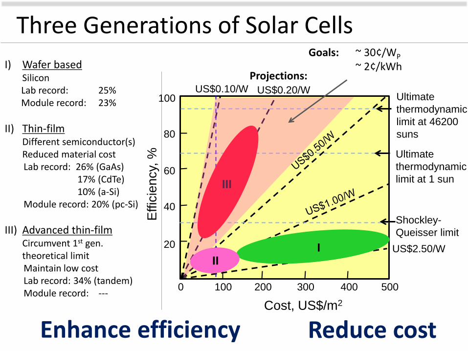
Three Generations of Solar Cells I) Wafer based Silicon Lab record: 25% Module record: 23% II) Thin-film Different semiconductor(s) Reduced material cost Lab record: 26% (GaAs) 17% (CdTe) 10% (a-Si) Module record: 20% (pc-Si) III) Advanced thin-film Circumvent 1st gen.
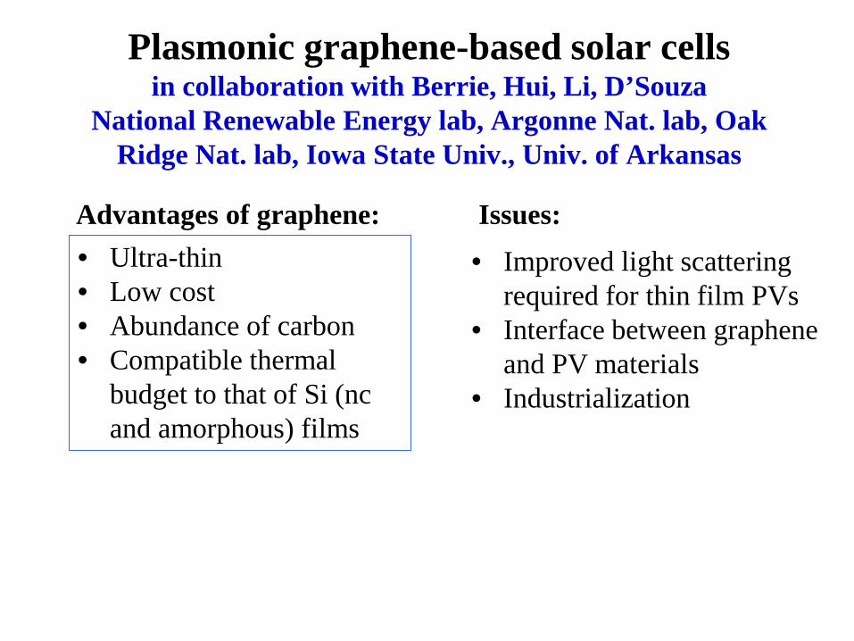
Advantages of graphene: • Improved light scattering
required for thin film PVs • Interface between graphene
and PV materials • Industrialization
Issues:
9
Graphene: a promising transparent electrode • Massless Dirac fermions with high Fermi speed
Vf~106 m/s • high mobility μ ~106 cm2/Vs • σ=enμ—high conductivity σ at low carrier density n
due to high μ; σmin ~4e2/h even at low carrier density
Optical Properties of Graphene • Gapless semiconductor or semi-metal • Fresnel equation in thin film limit: Transmittance—
Absorption –
Reflection – <0.1%
• Transparent conductors • IR detectors • Bio-/chemical-sensors
10 P. Avouris, Nano Letters 10, 4285(2010)
11
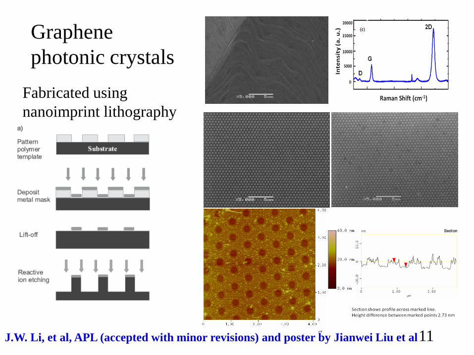
Graphene photonic crystals
Fabricated using nanoimprint lithography
J.W. Li, et al, APL (accepted with minor revisions) and poster by Jianwei Liu et al
Optical Transmittance
Electrical Conductivity
12
Transmittance vs. conductivity
A unique scheme to improve both optical transmittance (broad band) and electrical conductivity
13
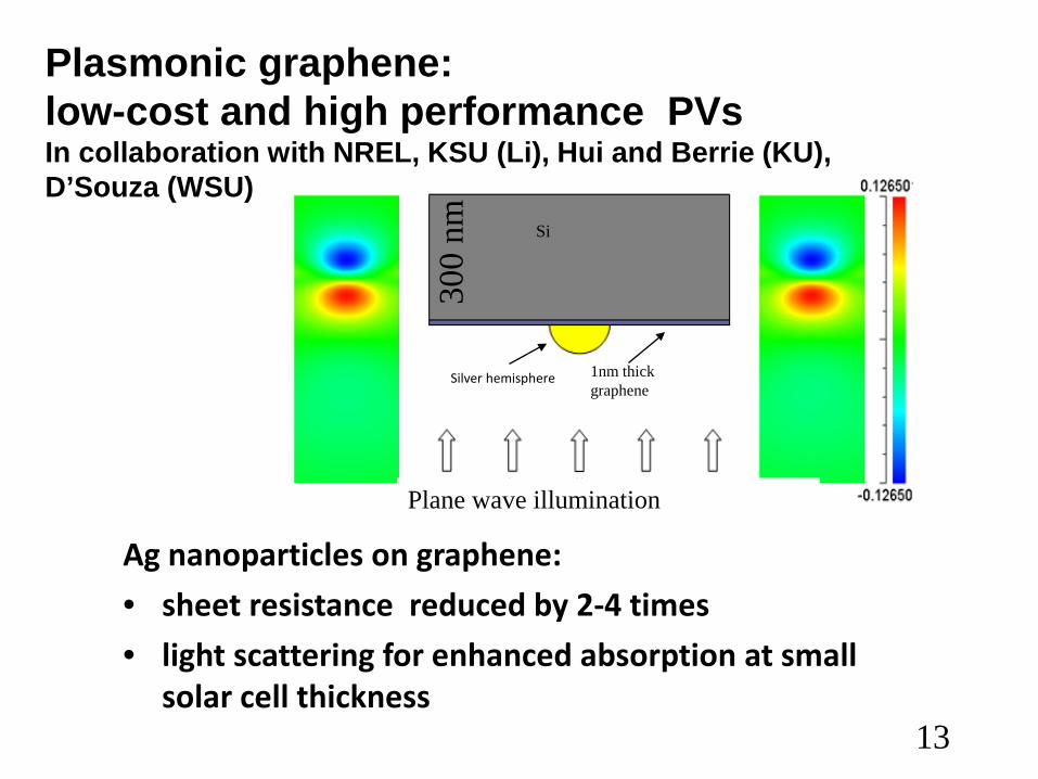
Ag nanoparticles on graphene: • sheet resistance reduced by 2-4 times • light scattering for enhanced absorption at small
solar cell thickness
Plasmonic graphene: low-cost and high performance PVs In collaboration with NREL, KSU (Li), Hui and Berrie (KU), D’Souza (WSU)
Si
Silver hemisphere 1nm thick graphene
Plane wave illumination
300
nm
14
Self-assembled Ag nanoparticles on graphene Diameter: 30-80nm
Ordered Ag nanoparticles on graphene Diameter: 150-250nm
A large range of controlled geometry has been demonstrated.
Generating plasmonic graphene
Poster by Guowei Xu et al, preprint.
15
• 10 times enhanced Raman peaks suggest strong light scattering on plasmonic graphene
• Confirmation of light scattering also in transmission spectra
• 2-4 times enhanced conductivity
Enhanced light scattering in plasmonic Graphene
300 400 500 600 700 8000.0
0.1
0.2
0.3
0.4
0.5
0.6
0.7
0.8
0.9
1.0
1.1
G_14nm AgNPs G_8nm AgNPs G_4nm AgNPs
Tran
smitt
ance
Wavelength (nm)
16
Summary Carbon-based nanostructures provide a fascinating system for physics studies and are promising for many optical and opto-electronic applications
University of Kansas Thin Film and Nanoscience Group July 27, 2010
17
Dr. Jianwei Liu Guowei Xu Caitlin Rochford Dr. Rongtao Lu Dr. Fengli Wang Dr. Bing Li Caleb Christianson Alan Elliot Gary Melek Logan Wille Mike Dunaway Jon Gregory Richard Lu
External collaborations: ANL: Zhijun Chen and Vic Maroni LANL: Javier Baca ORNL: Amit Goyal and Parans Paranthaman NREL: Yanfa Yan