11

2 3Strategy, MissionPolifab, Vision
Polifab Strategy
MissionVision
Polifab is the open-access, micro and nanofabrication facility of Politecnico di Milano, created to provide the highest technological standards for a wide range of applications and processes involving the Key Enabling Technologies: photonics, micro and nanoelectronics, biotechnologies, advanced materials and nanotechnology. Polifab houses 8M€ of nanofabrication and technological tools in a 370 m2 cleanroom, managed by three technicians and staff personnel from research groups of Politecnico di Milano. The cleanroom is equipped with advanced instrumentation for the research and development of new materials, technological processes and devices at the micro- and nano-scale. Polifab is located in the academic environment of the Campus Leonardo of Politecnico di Milano.
At Polifab, enabling technologies are blended in a multidisciplinary environment, where each scientific branch is synergic to the others. Mastering these technologies means being at the forefront of the route towards knowledge-based economy. Cross-fertilization of knowledge is the future of science and education, as well as the keystone for innovation and competitiveness of both academic and industrial research.
Polifab targets fundamental, applied and commercial research and development in collaboration with universities, research institutes and industries. It supports and stimulates the development of technologies, materials, devices, systems and solutions, generating an IP portfolio of multidisciplinary competencies. Polifab acts as nucleation center for the creation of laboratories clusters and joint research activities, promoting research and education in the key emerging technologies. Three research laboratories, from the Department of Electronics, Information and Bioengineering (DEIB) and the Department of Physics, are built around Polifab since its foundation.
The mission of Polifab is to support and boost micro and nanotechnology activities carried out by research groups of Politecnico di Milano, external research institutions and industries. Polifab aims at aggregating users active in education, scientific research, development and prototyping through collaborations and strategic alliances with external partners. As a consequence of this catalytic action, Polifab users gain competitiveness on the European scenario.
8M€of nanofabrication and technological tools
370 m2cleanroom
Cross-fertilization of knowledgeis the future of science and education
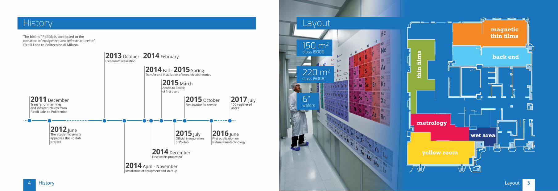
4 History
2011 DecemberTransfer of machinesand infrastructures fromPirelli Labs to Politecnico
2014 DecemberFirst wafers processed
2015 MarchAccess to Polifabof �rst users
2015 JulyO�cial inaugurationof Polifab
2017 July100 registeredusers
2012 JuneThe academic senateapproves the Polifabproject
2015 OctoberFirst invoice for service
2016 JuneFirst publication onNature Nanotechnology
2014 April - NovemberInstallation of equipment and start up
2013 October - 2014 FebruaryCleanroom realization
2014 Fall - 2015 SpringTransfer and installation of research laboratories
The birth of Polifab is connected to the donation of equipment and infrastructures of Pirelli Labs to Politecnico di Milano. 150 m2
class ISO06
6’’wafers
History Layout
wet area
metrology
back end
magnetic thin films
thin
film
s
yellow room
220 m2class ISO08
Layout 5

6 7Processes and equipmentProcesses and equipment
Processes and equipment
Photo and electrom beam lithography
Mask Aligner - Karl Süss MA6/BA8: 1000 W mercury lamp, proximity, soft, hard and vacuum contact, back side alignment.
Maskless Aligner - Heidelberg MLA100: 365 nm wavelength, substrates up to 8” x 8”, write speed of 50 mm²/min, grey-scale with 256 levels.
SEM and EBL System - LEO 1525 / Raith Elphy Plus: high resolution FE-SEM, accelerating voltages from 0.5 kV to 30 kV. EBL resolution: 20 nm. Samples up to 2”.
Spin Coater - Karl Süss RC8: with adapters for samples from 1” to 6”.
Hot Plates: temperature range: 25 - 250 °C, accuracy: +/-1 °C, from fragments to wafers up to 12”.
Wet benches + Spin Rinse and Dryer - Semitool: resist development and wafer cleaning.
Optical Microscope - Leica INM 200: motorized x-y stage, visible and UV light, objectives from 2.5x to 100x.
Chemical Vapor Deposition - STS Multiplex: for SiO2, SiOxNy, SiN, a-Si:H deposition, Gas: SiH4, NH3, N2O, O2, CF4, substrates up to 8”.
Magnetron sputtering systems - Leybold LH Z-400 and Kenosistec VS80: DC and RF for metals and oxides (Cr, Au, ITO, SiO2, SiC), substrates up to 3”.
E-beam Evaporator - Evatec BAK 640: 6 pockets rotating crucible, up to nine 6” wafers per run, metals and oxides.
Pulsed Laser Deposition: 1” samples, Nd:YAG Q-switch laser.
Molecular Beam Epitaxy: UHV deposition of metals and oxides.
Electroplating: Deposition of Au and Ni on 1-2” samples.
ICP Reactive ion etching - Oxford Plasmalab 100: RIE power up to 600 W and ICP power up to 2000 W, SF6, O2, CHF3, C4F8 gases.
Ion beam etching - Kaufman source KDC 160: Ar gas, beam voltage 200 - 850 V, motorized rotating and tilting holder, ±15% thickness uniformity on 6” wafers.
Plasma Asher - PVA TEPLA 200: Ar and O2 gas, maximum power 400 W.
The cleanroom is designed to operate on substrates up to 6 inches.
Dry etching
Thin films deposition

8 9
Dicing saw - DISCO DAD 341: including wafer mounting and cleaning for semiconductor, ceramic and glass wafers.
Automatic wafer diamond scriber - Dynatex GST-150: < 5 μm scribe line, adjustable scribe angle, scribe speed up to 10” per second.
PDMS and microfluidic facilities: including spin coater, hot plate, drying oven.
Ball bonder - Kulicke & Soffa 4124: Au wire, 95 x 95 mm2 bonding area.
Wet processes
Back-end
Wet benches for chemical etching: acids and bases with heated reaction baths and automatic rinse/drain tanks for single- and multi-wafer process.
Wet benches for lift-off: solvents with heated reaction baths and sonicator.
Annealing
Drying oven - Heraeus UT6060: low temperatures curing (300 °C).
Muffle furnace - Nabertherm LT 9/11 SKM: up to 1100 °C in 90 minutes, 9 l internal volume, under N2 flux.
Horizontal quartz tube furnace - Carbolite Gero KST 12/600: up to 1200 °C, inert atmosphere during heating (N2) and annealing in vacuum.
Atomic force microscope - Keysight 5600LS: substrates up to 8”, fully addressable and programmable stage, Magnetic, Electrostatic, Kelvin Probe and Piezoresponse Force Microscopies.
Electric Probe System - SÜSS MicroTec PM5: with heated chuck.
Spectroscopic ellipsometer - J.A. Woollam VASE: 260 nm 1700 nm, incidence angle from 15 to 90 degrees, up to 8” wafers.
Stylus profilometer - KLA Tencor P15: measured thickness in the range 10 nm - 327 µm, 3D topography mapping, stress measurement.
Prism coupler - Metricon: thickness and refractive index measurement, 632.8 nm, 1320 nm and 1554 nm wavelength.
Optical microscope - LEICA FTM 200: three axes, motorized, with autofocus.
Wafer thickness measurement - Eichhorn & Hausmann MX 203: thickness range 400 - 1000 µm, resolution 1 µm.
Characterization
Processes and equipmentProcesses and equipment
10 How to access
Polifab is an open-access, pay-per-use facility, open to research groups of Politecnico as well as to external research institutions and industries.Researchers can enter the cleanroom and become users of the facilities, after specific training courses given by the technical staff of Polifab. Processes can be run directly by the technical staff of Polifab and offered as a service to external companies or research groups. To access the cleanroom facilities first contact the Polifab staff to discuss your technological needs, verify the feasibility of your ideas, and identify the model of use: service or user.
Shared access to cleanroom facilities is regulated by a booking system available in the Polifab intranet.Information on the booking procedure can be found on our website: www.polifab.polimi.it
Service model
User model
Booking
The Polifab staff executes the required processes, characterization or prototyping within the framework of a research or service contract. No direct access of personnel from the external group or company is required.
New cleanroom users must attend a safety course and obtain a Polifab access certificate. Specific machine and process training is given by the technical staff of Polifab.
Information on the cleanroom status, machine maintenance and operation, and access limitations are shared with all the users through the Polifab mailing list.
How to access Organization chart
AdvisoryBoard
Prof. Andrea Leonardo LacaitaProf. Riccardo BertaccoProf. Alberto CoriglianoProf. Ferruccio Resta
Prof. Sandro De SilvestriProf.ssa Marinella LeviIng. Bruno MunariProf. Rinaldo Cubeddu
Staff
Deputy DirectorRiccardo Bertacco
Cleanroom managerClaudio Somaschini
TechnicianLorenzo Livietti
Process specialistAlessia Romeo
DirectorAndrea Leonardo Lacaita
11Organization chart
Advisory Board5 internal members,from Departments
of Politecnico(+2 external advisors)
Director(Deputy director)
StaffCleanroom manager
Process specialistTechnician
Users
Area Servizi Supportoalla Ricerca
General director ofPolitecnico di Milano

12 13HighlightsHighlights
Patterning of ferroelectric domains by Piezoresponse Force Microscopy
100 μm 5 μm
300 nm
RIE on SiO2
Epitaxial growth and patterning of ferroelectric and magnetic materialsM. Asa, S. Varotto, C. Rinaldi, M. CantoniDepartment of Physics - Politecnico di Milano
Develoment of resistive switches for in-memory computingA. Bricalli, D. IelminiDepartment of Electronics, Information and Bioengineering - Politecnico di Milano
Reversible patterning of spin textures in ferromagnetsE. Albisetti, D. PettiDepartment of Physics - Politecnico di Milano
Thermally assisted magnetic scanning probe lithography (tam-SPL)
Magnetic patterning of spin textures
Excitation and channelling of spin-waves
Memristors crossbar array
2D transistor with nanoscale channel
100 nm 50 nm 30 nmp+-Si
SiO2
Source Drain
Gate
Gap
2D mat.
Transmission electron microscopy image of a Cr2O3 /BaTiO3 heterostructure grown by PLD and MBE
Highlights
14 15
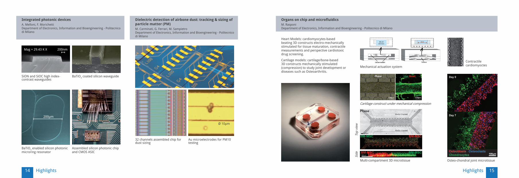
BaTiO3 coated silicon waveguide
BaTiO3 enabled silicon photonic microring resonator
Assembled silicon photonic chip and CMOS ASIC
SiON and SiOC high index-contrast waveguides
Heart Models: cardiomyocytes-based beating 3D constructs electro-mechanically stimulated for tissue maturation, contractile measurements and perspective cardiotoxic drug screening.
Cartilage models: cartilage/bone-based 3D constructs mechanically stimulated (compression) to study joint development or diseases such as Osteoarthritis.
Cartilage construct under mechanical compression
Mechanical actuation system
Multi-compartment 3D microtissue
Contractile cardiomyoctes
Osteo-chondral joint microtissue
Top
view
Side
Integrated photonic devicesA. Melloni, F. Morichetti Department of Electronics, Information and Bioengineering - Politecnico di Milano
Dielectric detection of airbone dust: tracking & sizing of particle matter (PM)M. Carminati, G. Ferrari, M. Sampietro Department of Electronics, Information and Bioengineering - Politecnico di Milano
Mag = 29.43 K X 200nm
200µm
Organs on chip and microfluidicsM. Rasponi Department of Electronics, Information and Bioengineering - Politecnico di Milano
HighlightsHighlights
32 channels assembled chip for dust sizing
Au microelectrodes for PM10 testing
Ø 10µm

16 Figures of merit
Prototype of diagnostic apparatus
Arrays of sensors based on magnetic tunnel junctions
Signals during a bioassay
Fe Head
5 µm
PDMS pillar
Active mechanical stimulation of single cells on Fe coated PDMS micro-pillars
Magnetically actuated micro-pillars for mechanobiologyM. Monticelli, R. Bertacco Department of Physics - Politecnico di Milano
Magnetic sensors based on tunneling junctionsE. Albisetti, D. Petti, R. Bertacco Department of Physics - Politecnico di Milano
50 µm
Highlights
Figures of merit
Incomings
40%Companies
30%Internal users
30%External users
Registered users 77 110
1st year(2016)
2nd year(2017)
12 17Research groups accessing Polifab
3 7Contracts with companies
2 4ERC projects based at Polifab
17 19Other research projects
50 60Students accessing Polifab for didactical and training activities
17

18 Contacts
Polifab - Politecnico di MilanoVia Giuseppe Colombo, 8120133 - Milano
www.polifab.polimi.it/venue
Venue
Contact us
Contacts
Visit our website:
www.polifab.polimi.it

20 Polifab
www.polifab.polimi.it


