52
Power Consumption Dr. Sachin D. Pabale Matoshri College of Engineering and Technology
| Date post: | 16-Feb-2017 |
| Category: |
Engineering |
| Upload: | sdpable |
| View: | 391 times |
| Download: | 0 times |
Power Consumption
Dr. Sachin D. Pabale
Matoshri College of Engineering
and Technology

Motivation to estimate power dissipation
Sources of power dissipation
Metrics
Power optimization Techniques
Conclusion
Outlines

Moore’s Law
• Blessing of technology Scaling:
Transistor count get double every 2 years
• Direct consequence of technology scaling:
Power density of IC increases exponentially at each
technology generation.

Power Dissipation
CMOS technology is scaling to meet the
1. Performance
2. To reduce the cost
3. Power requirement
However, static power dissipation increases
considerably which is primarily due to the
flow of leakage currents.

Figure 2.1: Normalized dynamic and static power dissipation for (W/Lg=3)
devi e. Data is ased o the ITRS [ 6] a d or alized to the year ’s figure [2].

Power Dissipation
Performance
Cost
Portability Packaging
Reliability
Power dissipation affects:
Need to estimate power dissipation

1999 2002 2005 2008 2011 20140
50
100
150
200
Year
Pow
er (
Wat
ts)
High performance microprocesssor chip
Hand held products
Figure 2.2: Power requirements of high performance
microprocessor chip and handheld products as per ITRS
[16].

KHz , nW • RFIDs
• Biomedical Sensors
MHz, µW • Embedded, ASICs
• Mobile electronics
GHz, W
• Servers
• Workstation
• Notebooks
Exploring Applications Space

Where does power goes in CMOS?
Dynamic power consumption
Short circuit power dissipation
Static/ leakage power
consumption

Power Consumption in CMOS
Leakage reduces
Delay
Delay
DDscpeakleakDDleak
2
DD V f tI tf V I V f loadtotal CP
Pdynamic
PStatic
Pshort-circuit

1. Dynamic power dissipation
VDD
Vin
VOUT
CL

Dynamic capacitive power and energy stored
in PMOS device Case I: When input is at logic 0: Power dissipation in PMOS is,
The current and voltages are related by,
CL
VDD
Vin VO
VSD
)( ODDLSDLP VViViP
dtdvCi oLL /Similarly, energy dissipation in the PMOS,
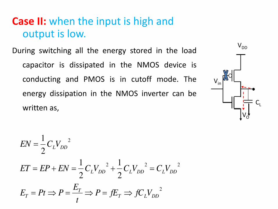
Case II: when the input is high and
output is low.
During switching all the energy stored in the load
capacitor is dissipated in the NMOS device is
conducting and PMOS is in cutoff mode. The
energy dissipation in the NMOS inverter can be
written as,
VO
CL
VDD
Vin
2
222
2
2
1
2
1
2
1
DDLTT
T
DDLDDLDDL
DDL
VfCfEPt
EPPtE
VCVCVCENEPET
VCEN
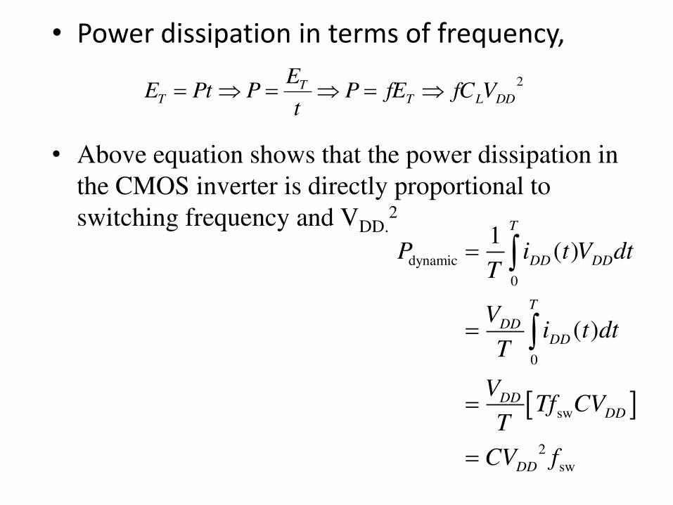
• Power dissipation in terms of frequency,
• Above equation shows that the power dissipation in
the CMOS inverter is directly proportional to
switching frequency and VDD.2
2
DDLTT
T VfCfEPt
EPPtE
dynamic
0
0
sw
2
sw
1( )
( )
T
DD DD
T
DDDD
DDDD
DD
P i t V dtT
Vi t dt
T
VTf CV
T
CV f

Dynamic capacitive power
• Dynamic power:
Observations:
Does not depends on device size
Does not depends on switching delay
Applies to general CMOS gate in which,
• Switch cap. are lumped into CL
• Output swing from GND to VDD
• Gate switches with frequency f
2
DDLdynamic VfCP

Lowering Dynamic Power
2
DDLdynamic VfCP Function of fan-out,
wire length, transistor
sizes
Supply Voltage: Has been reduced with
successive generation
Clock frequency
Increasing…..

100
102
104
10-11
10-10
10-9
10-8
10-7
10-6
10-5
Frequency (KHz)
Pow
er d
issp
atio
n (
W)
VDD=0.35V
VDD=0.4V
VDD=0.9V
VDD=1.2V
superthreshold
regime
Subthreshold
regime
Figure 2.13: Power dissipation as a function of
operating frequency.
Power as function of Frequency

Finite slope of input signal causes a
direct current path between VDD and
GND for short period of time.
i.e. Short circuit current flows from
VDD to GND when both transistors
are on.
Short Circuit Power Consumption
VDD
Vin VOUT
CL

Short Circuit Power Consumption
Vin
Vth
VDD - Vth
t
I short
I max
0 50 100 150 200 250 300 350 4000
100
200
300
400
0 50 100 150 200 250 300 350 4000
1000
2000
3000
4000
Input voltage (mV)
Ou
tpu
t v
olt
ag
e (
mV
)
Cu
rren
t (p
A)
Vout short circuit leakage
Transition
32nm NMOS
VDD=0.4V
Figure 2.4: Short circuit leakage
current of inverter at 32 nm technology
node and VDD=0.4V.

• Approximate short circuit current as triangular
wave.
• Energy per cycle,
Short Circuit Power Consumption
2
2
2
2
max
maxmaxmax
fr
DDSC
fr
DDr
DDr
DDSC
ttfIVP
ttIV
tIV
tIVE
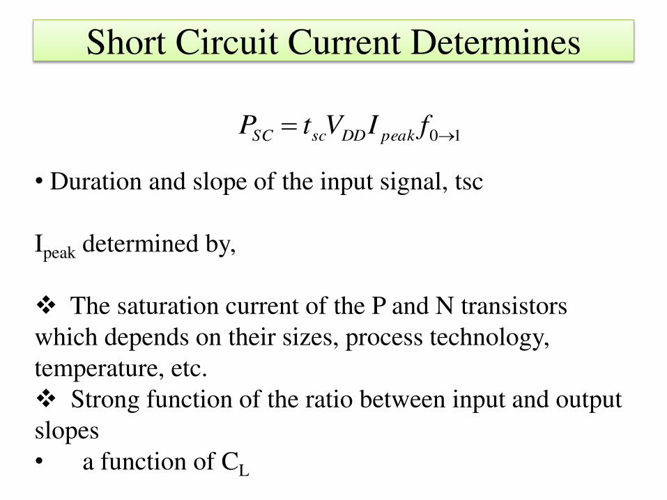
Short Circuit Current Determines
10 fIVtP peakDDscSC
• Duration and slope of the input signal, tsc
Ipeak determined by,
The saturation current of the P and N transistors
which depends on their sizes, process technology,
temperature, etc.
Strong function of the ratio between input and output
slopes
• a function of CL

Impact of CL on PSC
VDD
Vin
VOUT
CL
Large Capacitive Load
ISC≈ 0
VDD
Vin VOUT
CL
Small Capacitive Load
ISC≈ Imax
Short circuit dissipation is minimized by matching the
rise/ fall times of the input and output signals.

As capacitive load increases short circuit power
decreases

Static Power Dissipation
• The static power is defined as the power consumption due to
constant current from VDD to ground in the absence of switching
activity.
• Shrinking transistor geometries causes different sources of
leakage current [16].
punchthrough
GateB D
Sub-threshold
p-n junctionp-n junction
p-well
p+
Gate leakage
S
GIDL leakage
n+ n+
Substrate
punchthrough
GateB D
Sub-threshold
p-n junctionp-n junction
p-well
p+
Gate leakage
S
GIDL leakage
n+ n+
Substrate

• Sources of static power dissipation
Reverse bias pn- junction current
Subthreshold leakage current
Gate leakage current
Gate-Induced Drain Leakage current
Punchthrough Leakage current
Static Power Dissipation

1. Reverse bias pn- junction current is flowing
due to,
minority carrier diffusion/drift near the edge of
the depletion region;
electron-hole pair generation in the depletion
region of the reverse-biased junction [12].
The magnitude of the diode’s leakage current depends on the area of the drain diffusion and
the leakage current density.

• In the presence of a high electric field (4106
V/cm) electrons will tunnel across a reverse-
biased p–n junction.
• Process technologies are generally well
designed to keep this pn-junction leakage
small relative to the subthreshold current.

2. Subthreshold leakage Current
• Subthreshold or weak inversion conduction
current between source and drain in an MOS
transistor occurs when gate voltage is below
[15].
)(
DSV)DSVthVGSV(
TUTnU0DsubD e1eIII
TT
2T
s
cheffsi
eff
effsubD
U1
nUU
2
Nq
L
WII DSthGS V
exp VV
exp

0 100 200 300 400 500 600 700 800 90010
-3
10-2
10-1
100
101
102
VGS (mV)
Dra
in C
urr
en
t (u
A)
IOFF
Vth=0.49V
Subthreshold region Superthreshold region
Isub
VGS <Vth
L
n+ n+
p-Substrate
S
VDS<Vth
TOX
D
Isub
NMOS transistor with bias voltages. I-V characteristics of NMOS transistor.
Subthreshold leakage Current

3. Gate leakage current
• As technology scales down, the oxide thickness gets
thinner which causes high electric field across the
oxide.
• As TOX scales below 3 nm, gate to channel leakage
current starts to appear even at low gate voltage. That
results in direct tunneling of electrons from substrate to
gate and gate to substrate through the gate oxide.

Gate leakage current
OX/OXV
)2/3)OX/OXV1(1(Bexp2)
oxToxV
(AeffLeffWgateI
oxh16
3qA
hq3
2/3oxm24
B
The gate leakage expressed in [32] is given by equation as follows,
where ‘VOX’ is the potential drop across the thin oxide layer, ‘
is the barrier height for the tunneling particles, ‘TOX’ is the oxide thickness, ‘A’ and ‘B’ are physical parameters.
‘
ox
Gate tunneling current has very strong dependence on the voltage
across the gate.

4. Gate induced drain leakage
• In the overlapping zone between gate and
drain, a high electric field exists, leading to the
generation of current from the edge of drain
and terminating at the body of the transistor.
• Thinner oxide thickness and higher potential
between gate and drain enhance the electric
field and therefore increase GIDL.

5. Puchthrough leakage current
• In short-channel devices, the depletion regions at the
drain-substrate and source-substrate junctions extend
into the channel.
• As the channel length is reduced, if the doping is kept
constant, the separation between the depletion region
boundaries decreases.
• When the combination of channel length and reverse
bias leads to the merging of the depletion regions,
punchthrough is said to have occurred.

Inverter Power consumption
• Total Power consumption
leakDD
fr
DDDDLtot
statscdyntot
IVftt
IVfVCP
PPPP
)2
(max
2

Power Reduction
1. Dynamic Power
Lower the voltage
Reduce capacitance
Reduce frequency
2. Reducing short-circuit current
Fats rise/ fall time on input signal
Reduce input capacitance
Insert small buffers to clean up slow i/p
3. Reducing leakage current
Small transistors (leakage proportional to width)
Lower voltage

Power Optimization Methodology
Multiple VDD
Multiple VDD -Multiple Vth
Gate sizing
Transistor sizing
Power gating
Transistor stacking and sleepy stacking
Multi-threshold architectures
Adaptive body biasing

Dual Power Supply
Dual Power Supply
lowering the VDD along non-critical
delay paths or light workloads and
higher VDD for heavy workloads .
The main problem of designing dual
VDD in CMOS circuits is the increased
leakage current in the high voltage
gates, when a low voltage gate is
driving them.
VDDL
Vin
Static current
VOut
Static current
VDDHVDDL
Vin
Static current
VOut
Static current
VDDH

Gate and Transistor sizing
• For non critical path reduce device size to
minimize the power consumption.
• In Gate sizing techniques all transistors in gate
is having size.
• In transistor sizing, within a gate transistors
may have different size to maximize the power
saving.

Leakage Power Reduction Techniques
Power Gating and Multi-
Threshold Voltage
In the ACTIVE mode, the sleep transistor is ON.
In the STANDBY mode, the sleep transistor is turned OFF.
____
Sleep
Sleep
Virtual VDD
Virtual Ground
In Out
P
N
____
Sleep
Sleep
Virtual VDD
Virtual Ground
In Out
P
N
“Higher Vth devices are preferred for sleepy
transistors to reduce leakage current.” - Multi-threshold architecture

VDD
VDDV
Standby
Bypass
capacitance
High-Vth sleep
transistor
Low-Vth logic
Transistor
GND
Power Gating and Multi-Threshold Voltage
MTCMOS Logic
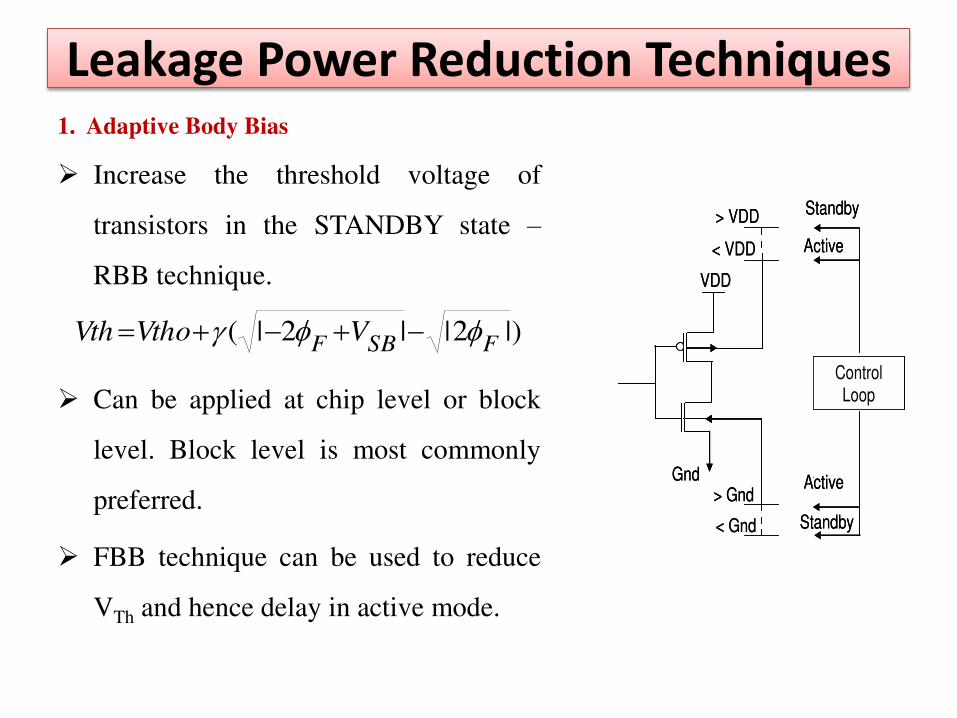
1. Adaptive Body Bias
Increase the threshold voltage of
transistors in the STANDBY state –
RBB technique.
Can be applied at chip level or block
level. Block level is most commonly
preferred.
FBB technique can be used to reduce
VTh and hence delay in active mode.
Leakage Power Reduction Techniques
)|2||2|(FSBF
VVthoVth
Gnd Active
Standby< Gnd
> Gnd
VDD
Active
Standby> VDD
< VDD
ControlLoop
Gnd Active
Standby< Gnd
> Gnd
VDD
Active
Standby> VDD
< VDD
ControlLoop
ControlLoop

Dynamic supply voltage scaling schemes
• Uses variable supply voltage and speed tech.
• The highest supply voltage delivers the highest performance at the fastest designed frequency of operation.
• When performance demand is low, supply voltage and clock frequency is lowered, just delivering the required performance with substantial power reduction [41].

DVS system
• Processor speed is controlled by software program automatically
• Supply voltage is controlled by hard-wire frequency–voltage feedback loop, using a ring oscillator as a critical path replica.
• All chips operate at the same clock frequency and same supply voltage, which are generated from the ring oscillator and the regulator.

Higher oxide thickness.
• To obtain high Vth devices
• To reduce subthreshold leakage current
• To reduce gate tunneling leakage current
• However, in case of severe SCE an increase in the oxide
thickness will increase the subthreshold leakage.
• In order to suppress SCE, the high tox device needs to
have a longer channel length as compared to the low tox
device [47]
• Advanced process technology is required for fabricating
multiple tox CMOS.

Clock gating
• Clock gating is an effective way of reducing the dynamic power dissipation in digital circuits.
• In a typical synchronous circuit such as the general purpose microprocessor, only a portion of the circuit is active at any given time. Hence, by shutting down the idle portion of the circuit, the unnecessary power consumption can be prevented.
• This prevents unnecessary switching of the inputs to the
idle circuit block, reducing the dynamic power.

Subthreshold Operating region
Low voltage of Operation

Power Consumption
Power consumption has become a significant hurdle for recent ICs
Higher power consumption leads to
• Shorter battery life
• Higher on-chip temperatures – reduced operating life of the chip
• Such applications are ideal candidates for sub-threshold circuit design.
• OK, so what is sub-threshold design??
There is a large and growing class of applications where
power reduction is paramount – not speed.

Ultra Low Power Circuit Design
Need: Power aware design increases considerably due to
remarkable growth of portable applications.
Remarkable power requirement gap between high performance microprocessor chip and portable device.
Increased leakage power density can not be ignored in case of portable devices.
To enhance the battery life time
KHz , nW RFIDs tags
Biomedical Sensors
etc
• Designing Subthreshold Circuits
How to
satisfy
ULP
demand?

Minimum Operating Voltage
• Swanson and Meindl (1972) examined the VTC of an inverter:
Minimum Voltage = 8kT/q or 200 mV at 300K
(A ring oscillator worked at 100 mV soon thereafter.)
• Ideal limit of the lowest possible supply voltage (2001) : VDD = 2kT/q ≈ 57 mV at 300K
• R. M. Swanson and J. D. Meindl, “Ion-Implanted Complementary MOS
Transistors in Low-Voltage Circuits,” IEEE JSSC, vol. 7, no. 2, April 1972. • A. Bryant, J. Brown, P. Cottrell, M. Ketchen, J. Ellis-Monaghan, E. Nowak, I.
Div, and E. Junction, “Low-power CMOS at Vdd= 4kT/q,” in Device Research Conference, 2001, pp. 22–23.

Subthreshold Regime (VDD
<Vth
)
VGS
<Vth
L
n+ n+
p-
Substrate
S
VDS<Vth
TOX
D
Isub
0 100 200 300 400 500 600 700 800 90010
-3
10-2
10-1
100
101
102
VGS (mV)
Dra
in C
urr
ent
(uA
)IOFF
Vth=0.49V
Subthreshold region Superthreshold region
Isub
Fig. 2.7 I-V characteristics of NMOS
transistor
Fig. 2.6 NMOS transistor with bias
voltages
TT
2T
s
cheffsi
eff
effsubD
U1
nUU
2
Nq
L
WII DSthGS V
exp VV
exp

Sub-Threshold Regime
Supply
Voltage Leakage Energy
Dissipation
Circuit Delay
Switching
Energy
Exponentially
2
total load DDE C V
total leak DD leakE I V t
/( )
0DD t
DD DDleak V nU
on
CV CVt
I I e
TT
2T
s
cheffsi
eff
effsubD
U1
nUU
2
Nq
L
WII DSthGS V
exp VV
exp
Subthreshold
regime
VDD< VTh
Exponentially
Quadretically
Sub-Threshold Regime
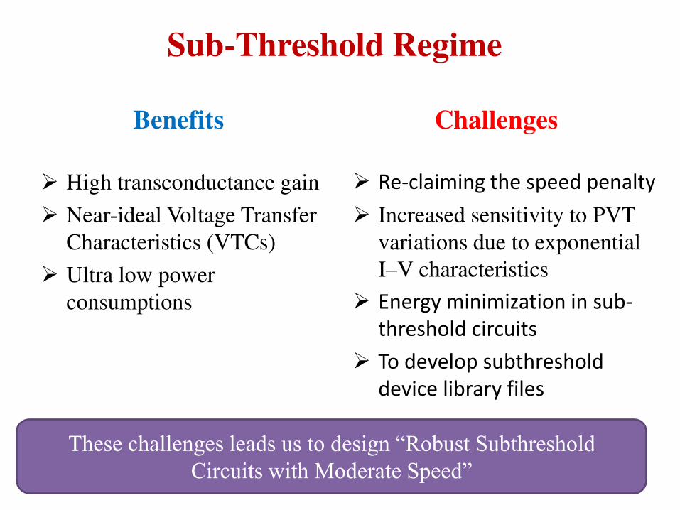
Benefits
High transconductance gain
Near-ideal Voltage Transfer
Characteristics (VTCs)
Ultra low power
consumptions
Challenges
Re-claiming the speed penalty
Increased sensitivity to PVT
variations due to exponential
I–V characteristics
Energy minimization in sub-
threshold circuits
To develop subthreshold
device library files
These challenges leads us to design “Robust Subthreshold
Circuits with Moderate Speed”


