23
Public Information P. Gassot, P. Moens, M. Tack, Corporate R&D Bodo Power Conference Munich, Dec. 2017 Power GaN Rdyn in hard and soft-switching applications

Public Information
P. Gassot, P. Moens, M. Tack, Corporate R&D
Bodo Power ConferenceMunich, Dec. 2017
Power GaN
Rdyn in hard and soft-switching applications
Public Information2 12/6/20172 12/6/2017
The authors wish to acknowledge and thank the University of Padova (Italy) and the University of Bristol (UK) for their significant contribution to this reliability investigation as well as our colleagues from ON Semiconductor who have effectively collaborated to this work.
References:• “Impact of buffer leakage on intrinsic reliability of 650V AlGaN/GaN HEMTs”, P. Moens, A.
Banerjee, M. J. Uren, M. Meneghini, S.Karboyan, I. Chatterjee, P. Vanmeerbeek, M. Cäsar, C. Liu, A. Salih, E. Zanoni, G. Meneghesso, M. Kuball, M. Tack, 2015 IEEE International Electron Devices Meeting (IEDM), Pages 35.2.1-35.2.4
• “Evidence of Hot-Electron Effects During Hard Switching of AlGaN/GaN HEMTs”, I. Rossetto; M. Meneghini; A. Tajalli; S. Dalcanale; C. De Santi; P. Moens; A. Banerjee; E. Zanoni; G. Meneghesso, IEEE Transactions on Electron Devices, 2017, Volume: 64, Issue: 9, Pages: 3734 - 3739
Acknowledgements

Public Information3 12/6/20173 12/6/2017
GaN MaterialBinary Crystal
Spontaneous Polarization due to electro-negativity difference between N-atoms and Ga-atoms
N=3.4, Ga=1.8
GaN High Electron Mobility Transistor
Low Ron high 2DEG ns~1x1013 cm-2
high 2DEG mobility ~2000cm2/VsHigh Breakdownwide bandgap (3.4 eV)Low Capacitanceno junctions (undoped)
No Qrr
AlGaN layerHigher Spontaneous
PolarizationN=3.4, Ga=1.8, Al=1.6
Piezoelectric polarizationdue to strained layer
2DEG: Ns HEMT ns~ 1013 cm-2
(Typical MOSFET ns ~1012 cm-2)

Public Information4 12/6/20174 12/6/2017
JEDEC Standard for Power Discrete Qualification:• Semiconductor Power discretes are currently qualified based on the JEDEC
Standard (JESD47/JEP122) developed for Silicon (Different activation energies for GaN so different testing conditions/models needed)
• The Statistical methods used to calculate failure rates are based on field returns and well identified failure modes (Limited knowledge built on GaN)
• The JEDEC standard does NOT provide any dynamic testing conditions, (The stability of dynamic electrical performance are crucial for GaN)
How to release GaN Power Devices to the market
1000h
10 YrsEa=2.1 eV[Whitman 2014]

Public Information5 12/6/20175 12/6/2017
JC-70.1: GaN Power Electronic Conversion Semiconductor Standards:
– Accelerate the Maturity of the Industry by Creating Credible Standards for GaN learning from the Past, Ramp Faster and Lower Risk to Customer
– Focus on Application & Usage in End Equipment and NOT on Harmonizing Devices, Process Equipment
New JEDEC Standard required for GaN
(Source: S.W. Butler, ‘Standardization for Wide Band Gap Devices: GaNSpec DWG’, APEC 2017)
Public Information6 12/6/20176 12/6/2017
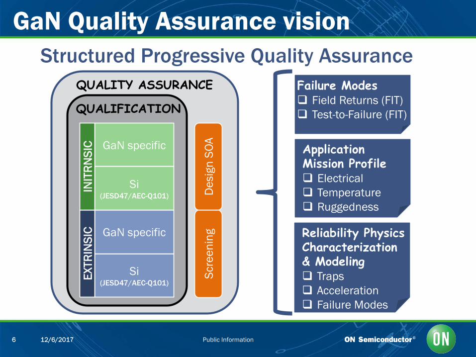
Structured Progressive Quality Assurance GaN Quality Assurance vision
Reliability PhysicsCharacterization& Modeling Traps Acceleration Failure Modes
Application Mission Profile Electrical Temperature Ruggedness
Failure Modes Field Returns (FIT) Test-to-Failure (FIT)
Si(JESD47/AEC-Q101)
GaN specific
EXTR
INSI
C
Si(JESD47/AEC-Q101)
GaN specific
INIT
RNSI
C
Scre
enin
g
QUALIFICATION
QUALITY ASSURANCE
Des
ign
SOA
Public Information7 12/6/20177 12/6/2017
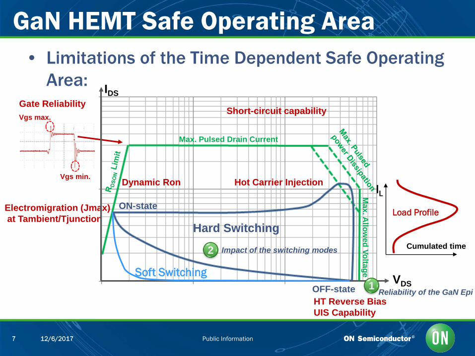
• Limitations of the Time Dependent Safe Operating Area:
GaN HEMT Safe Operating Area
Vgs min.
Vgs max.
Load Profile
Cumulated time
ILElectromigration (Jmax)at Tambient/Tjunction
HT Reverse BiasUIS Capability
Short-circuit capability
ON-state
OFF-state
Hard Switching
Gate ReliabilityIDS
VDSSoft Switching
Hot Carrier InjectionDynamic Ron
Max. Pulsed Drain Current
Max. A
llowed Voltage
1
2 Impact of the switching modes
Reliability of the GaN Epi

Public Information8 12/6/20178 12/6/2017
Reliability of the GaN EpiCorporate R&D
Bodo Power ConferenceMunich, Dec. 2017
1

Public Information9 12/6/20179 12/6/2017
• GaN Buffer behaves as a leaky dielectric– One VTLF : one dominant trap [Lampert, PhysRev1956]. In our case CN
– Above VTLF : steep voltage acceleration (Vn) due to Poole Frenkel
Reliability of the GaN Epi Buffer
Stressed at T=200°C Acceleration Model built & verified

Public Information10 12/6/201710 12/6/2017
Impact of the Switching ModesCorporate R&D
Bodo Power ConferenceMunich, Dec. 2017
2
Public Information11 12/6/201711 12/6/2017
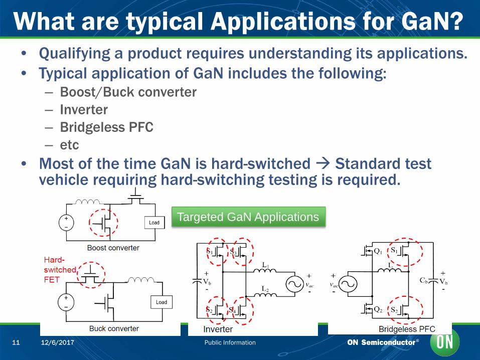
• Qualifying a product requires understanding its applications.• Typical application of GaN includes the following:
– Boost/Buck converter– Inverter– Bridgeless PFC– etc
• Most of the time GaN is hard-switched Standard test vehicle requiring hard-switching testing is required.
What are typical Applications for GaN?
Targeted GaN Applications
Public Information12 12/6/201712 12/6/2017
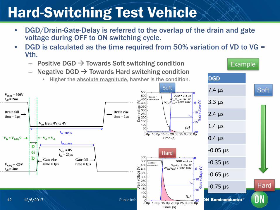
• DGD/Drain-Gate-Delay is referred to the overlap of the drain and gate voltage during OFF to ON switching cycle.
• DGD is calculated as the time required from 50% variation of VD to VG = Vth. – Positive DGD Towards Soft switching condition– Negative DGD Towards Hard switching condition
• Higher the absolute magnitude, harsher is the condition.
Hard-Switching Test Vehicle
VDSQ = 600Vtoff ≈ 2ms
Drain falltime = 1µs
Drain risetime = 1µs
DGD
ton_DRAIN
VDS from 0V to 4V
VGSQ = -20Vtoff ≈ 2ms
Gate rise time = 1µs
Gate falltime = 1µs
VGS = 0Vton = 20µs
VD = VDSQ/2 VG = Vthton_GATE
DGD
7.4 µs
3.3 µs
2.4 µs
1.4 µs
0.4 µs
-0.05 µs
-0.35 µs
-0.65 µs
-0.75 µs
Soft
Hard
Example
(a)
(b)
Soft
Hard

Public Information13 12/6/201713 12/6/2017
Measurement Conditions
DUT
VDD
VG
VS
RLOAD = 1kΩ
Pulsed IV (Double pulse setup): VG = -20VVDD/DS = from 0V to 600V, 100V/stepVS= Vchuck = 0V
Hard Switching stress: VG = 0V; VDD = As per the stress condition VDS measured by the custom probeIDS= IRLOAD = VRLOAD/RLOADVS= Vchuck = 0V
Temperature: Room and High temperature
Pulsed IDVD
Hard Switching Stress
(DGD ≈ varying)Pulsed IDVD

Public Information14 12/6/201714 12/6/2017
• Hard switching condition leads to a dynamic variation of the on-resistance.• The analysis of the on-resistance variation demonstrates that:
– Increase of the on-resistance is directly linked to decrease of DGD.– No degradation observed for Soft switching condition (comparable to fresh device). – Is the degradation off-state voltage acceralated?
Study of Possible Degradation
0 100 200 300 400 500 60010
12
14
16
18
20
On
resi
stan
ce (o
hm*m
m)
VDSQ (V)
DGD (us) 3.2us -0.2us -1us -1.06us -1.11us -1.17us -1.22us -1.27us
VGSQ = -20V, VGS = 0V
0 100 200 300 400 500 6001.0
1.1
1.2
1.3
1.4
1.5
On
resi
stan
ce v
aria
tion
(a.u
.)
VDSQ (V)
DGD (us) 3.2us -0.2us -1us -1.06us -1.11us -1.17us -1.22us -1.27us
Ronvariation = Ron(-20,VDSQ)/Ron(0,0)
Soft to Hard SwSoft to Hard Sw
VD,off=600V
Public Information15 12/6/201715 12/6/2017
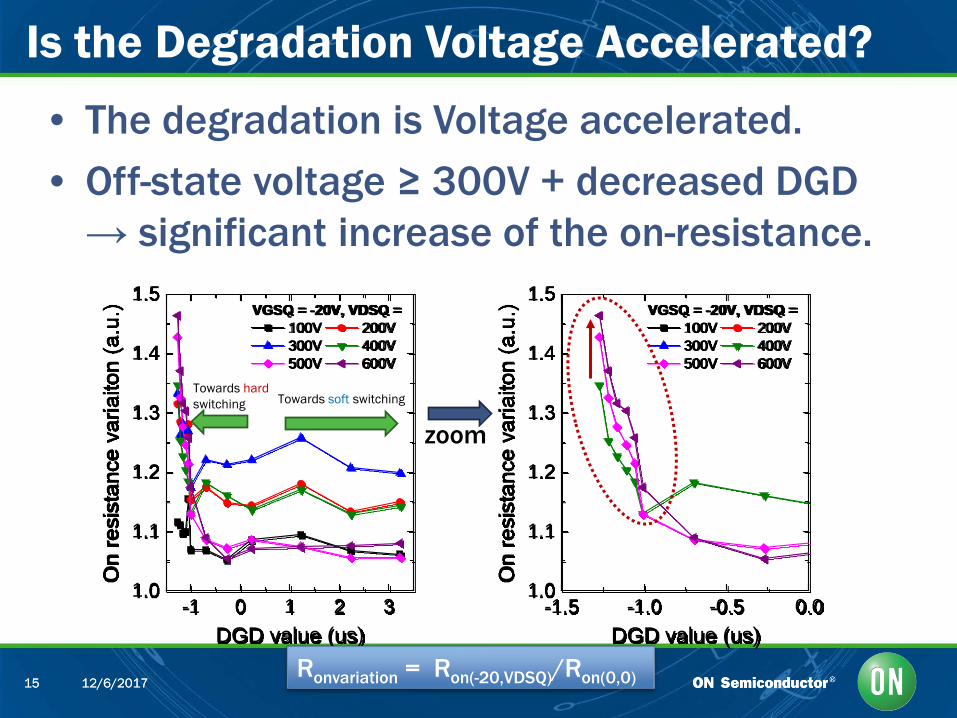
• The degradation is Voltage accelerated.• Off-state voltage ≥ 300V + decreased DGD
→ significant increase of the on-resistance.
Is the Degradation Voltage Accelerated?
-1 0 1 2 31.0
1.1
1.2
1.3
1.4
1.5
On
resi
stan
ce v
aria
iton
(a.u
.)
DGD value (us)
VGSQ = -20V, VDSQ = 100V 200V 300V 400V 500V 600V
-1.5 -1.0 -0.5 0.01.0
1.1
1.2
1.3
1.4
1.5
On
resi
stan
ce v
aria
iton
(a.u
.)
DGD value (us)
VGSQ = -20V, VDSQ = 100V 200V 300V 400V 500V 600V
Ronvariation = Ron(-20,VDSQ)/Ron(0,0)
zoomTowards soft switching
Towards hardswitching

Public Information16 12/6/201716 12/6/2017
• The dynamic variation of the on resistance changes with the ambienttemperature.– The change of the dynamic RON for VDSQ = 200V increases with
temperature, with the «Bump: shifting towards lower VDSQ.– At VDSQ = 600V the variation of the on-resistance slightly decreases with
temperature, presumably influenced by:• Increase of the detrapping process with temperature, detectable at both DGD = 3.3
µs and DGD = -0.65 µs.• Decrease of the influence of the hot electrons, detectable mainly at DGD = -0.65 µs.
Is the Degradation Temperature Accelerated?
Ronvariation = Ron(-20,VDSQ)/Ron(0,0)
(a) (b)

Public Information17 12/6/201717 12/6/2017
• Device degradation under hard switching condition is caused by Hot Electrons in the channel.• Higher the power dissipation Higher is the degradation.
• Recent TCAD[1] studies reported in literature points to similar facts.• Gate/Field plate edges (edge effect) suffer from high E-field in off-state,
leading to higher degradation in those localized areas.
Understanding of the Degradation Mechanism?
[1]: S. Bahl, et al, “Product level Reliability of GaN Devices”, IRPS 2016
Hot carrier related degradation during hard-switching turn-on

Public Information18 12/6/201718 12/6/2017
• Spatially resolved EL spectra confirms the hot electron related degradation during hard switching. – Decreasing DGD Higher EL
signal Higher degradation.– No emission observed for soft
switching condition.• EL/Degradation signal is
observed at the gate edge of the drain side. – Results in line with TCAD
understanding.
Emission Microscopy Results [1]
Gate
DGD = 0.4 µs
Drain
Gate
DGD = -0.4 µs
Drain
Gate
Drain
Gate
Drain
Gate
Drain
Gate
Drain
Gate
Drain
Gate
Drain
Gate
Drain
Gate
DGD = -0.75 µs
DGD = -0.85 µs
DGD = -0.9 µs
DGD = -0.95 µs
DGD = -1 µs
DrainGate
Hard Switching
Dec
reas
ing
DG
D
Soft Switching (DGD=3.3 us)

Public Information19 12/6/201719 12/6/2017
• Good correlation is noticed between the increase ofthe EL signal and of the dynamic on resistance.– Dynamic RDS,on increase can be attributed to hot
carrier type of degradation occurring in the accessregion (gate-drain).
Emission Microscopy Results [2]
-1.0µ 0.0 1.0µ 2.0µ 3.0µ600.0k
700.0k
800.0k
900.0k
1.0M
1.1M
1.2M
EL s
igna
l (a.
u.)
DGD (s)
acquisition time: 60sEM gain: 200
Trapping: (VGSQ,VDSQ) = (-20V,600V)
600.0k 800.0k 1.0M 1.2M13
14
15
16
17
DGD decrease
Dyn
amic
On
resi
stan
ce (o
hm*m
m)
EL signal (a.u.)
CCD cameranoise level
(VGSQ, VDSQ) =(-20V, 600V)
-1.0µ -800.0n -600.0n600.0k
700.0k
800.0k
900.0k
1.0M
1.1M
1.2M
acquisition time: 60sEM gain: 200
Trapping: (VGSQ,VDSQ)= (-20V,600V)
EL s
igna
l (a.
u.)
DGD (s)
ZOOM
Public Information20 12/6/201720 12/6/2017
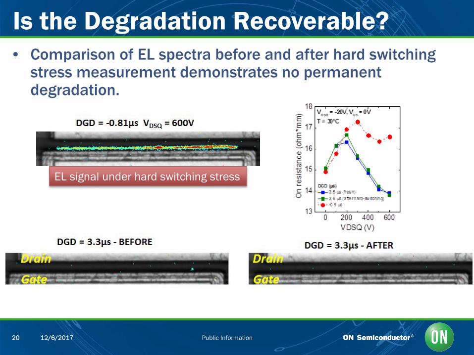
• Comparison of EL spectra before and after hard switching stress measurement demonstrates no permanent degradation.
Is the Degradation Recoverable?
EL signal under hard switching stress

Public Information21 12/6/201721 12/6/2017
• Two identical device layouts, different buffers (optimization for dyn Ron, lateral leakage current etc…)
Electro-luminescence as a means to define SOA
0 50 100 150 200
VDS
(V)
0
10
20
30
40
I DS
(mA
)
0
1
2
3
4
EL
(a.u
.)1W level
0 50 100 150 200
VDS
(V)
0
10
20
30
40
I DS
(mA
)
0
1
2
3
4
EL
(a.u
.)1W level

Public Information22 12/6/201722 12/6/2017
• A successful methodology is established for reliability assessment of GaN. – Initial demonstration on single finger devices shows good correlation with
understanding (& TCAD).– Measurement setup can be easily adapted (high flexibility) for powerbar
measurements.– Tests are done at wafer level Fast feedback
• High power dissipation during a hard-switching event is one of the major degrading factors for GaN power devices.– Hot electrons accelerated under high off-state bias leads to trapping in
access regions Dynamic RDSon increase.– Higher the power dissipation during hard-switching
event = Higher is the RDSon increase.– This degradation is NOT permanent– Degradation can be reduced by proper device
architecture (such as Field Plate design, etc)
Impact of the Switching Modes - Summary

Public Information23 12/6/201723 12/6/2017
• ON Semiconductors’ vision on Quality Assurance for GaN based power systems is presented:– Si JEDEC qualification to be extended with GaN specific tests, e.g. on Rdyn– Design SOAs are developed, supporting application mission profiles– Extensive screening tests are mandatory in the early years
• As an example, Rdson dispersion (Rdyn) is studied:– Impact demonstrated of hard switching vs soft switching applications.– SOA Design rules, enabling product design for high reliability applications
• Collective learning to result in a new Jedec standard specifically for GaN (JC-70).
Conclusions


