17
Never stop thinking. Power Management & Supply Datasheet Version 2.2, 04 Jul 2011
| Date post: | 06-Apr-2018 |
| Category: |
Documents |
| Upload: | phungkhanh |
| View: | 216 times |
| Download: | 2 times |

N e v e r s t o p t h i n k i n g .
Power Management & Supp ly
Datasheet Version 2.2, 04 Jul 2011

Edition 2011-07-04
Published byInfineon Technologies AG81726 Munich, Germany© 2007 Infineon Technologies AGAll Rights Reserved.
Legal DisclaimerThe information given in this document shall in no event be regarded as a guarantee ofconditions or characteristics. With respect to any examples or hints given herein, any typicalvalues stated herein and/or any information regarding the application of the device,Infineon Technologies hereby disclaims any and all warranties and liabilities of any kind,including without limitation, warranties of non-infringement of intellectual property rightsof any third party.
InformationFor further information on technology, delivery terms and conditions and prices, pleasecontact the nearest Infineon Technologies Office (www.infineon.com).
WarningsDue to technical requirements, components may contain dangerous substances. For informationon the types in question, please contact the nearest Infineon Technologies Office.Infineon Technologies components may be used in life-support devices or systems only withthe express written approval of Infineon Technologies, if a failure of such components canreasonably be expected to cause the failure of that life-support device or system or to affectthe safety or effectiveness of that device or system. Life support devices or systems areintended to be implanted in the human body or to support and/or maintain and sustainand/or protect human life. If they fail, it is reasonable to assume that the health of the useror other persons may be endangered.
For questions on technology, delivery and prices please contact the Infineon Technologies Offices in Germany orthe Infineon Technologies Companies and Representatives worldwide: see our webpage at http://www.infineon.com
CoolMOS™, CoolSET™ are trademarks of Infineon Technologies AG.
ICE2QS01
Revision History: 04 Jul 2011 Datasheet
Previous Version: 2.1
Page Subjects (major changes since last revision)
16 revised outline dimension.

Version 2.2 3 4 Jul 2011
ICE2QS01
PG-DIP-8
ICE2QS01
PG-DIP-8
Product Highlights
• Active burst mode for low standby power• Digital frequency reduction for better overall
system efficiency• Integrated power cell for IC self-power supply
Features• Quasiresonant operation till very low load• Active burst mode operation at light load for low
standby input power (< 1W)• Digital frequency reduction with decreasing load• Power cell for VCC pre-charging and IC power supply
during latch-off, or standby mode operation when it isnecessary
• Built-in digital soft-start• Foldback correction and cycle-by-cycle peak current
limitation• Auto restart mode for VCC Overvoltage protection• Auto restart mode for VCC Undervoltage protection• Auto restart mode for openloop/overload protection• Latch-off mode for adjustable output overvoltage
protection• Latch-off mode for Short-winding protection
DescriptionICE2QS01 is a quasi-resonant PWM controlleroptimized for off-line switch power supply applicationssuch as LCD TV, CRT TV and notebook adapter. Thedigital frequency reduction with decreasing loadenables a quasi-resonant operation till very low load.As a result, the system efficiency is significantlyimproved compared to other conventional solutions.The active burst mode operation enables an ultra-lowpower consumption at standby mode with small andcontrollable output voltage ripple. The innovativepower cell solves the IC power supply problem whenthe output voltage is pulled down during standbymode, or during latch-off mode. The numerousprotection functions give a full protection of the powersupply system in failure situations. All of these makethe ICE2QS01 an outstanding controller for quasi-resonant flyback converter in the market.
Typical Application
Type Marking Package
ICE2QS01 ICE2QS01 PG-DIP-8
85 ~ 265 VAC
SnubberCbus
Dr1
~Dr4
PowerCell
GND
REG
HV VCC ZC
OUT
CS
Power Management
Digital Process Block
Active Burst Mode
Protection Block
Current Mode Control
PWMController
GateDriverZero Crossing Detection
CurrentLimitation
ICE2QS01
RCSTL431
Optocoupler
Rb1
Rb2
Rc1
Cc1C
c2
Rovs2
Rovs1
CVCC
RVCC
DVCC
RZC2 RZC1
CZC
DZC
Wp
Ws
Wa
DO
CO
LfC
fV
O
CREG
CPS
CDS
Q1
Quasi-Resonant PWM Controller

Quasi-Resonant PWM ControllerICE2QS01
Table of Contents Page
Version 2.2 4 4 Jul 2011
1 Pin Configuration and Functionality . . . . . . . . . . . . . . . . . . . . . . . . . . . . .51.1 Pin Configuration . . . . . . . . . . . . . . . . . . . . . . . . . . . . . . . . . . . . . . . . . . . . . .51.2 Package PG-DIP-8 . . . . . . . . . . . . . . . . . . . . . . . . . . . . . . . . . . . . . . . . . . . .51.3 Pin Functionality . . . . . . . . . . . . . . . . . . . . . . . . . . . . . . . . . . . . . . . . . . . . . .5
2 Representative Block Diagram . . . . . . . . . . . . . . . . . . . . . . . . . . . . . . . . . .6
3 Functional Description. . . . . . . . . . . . . . . . . . . . . . . . . . . . . . . . . . . . . . . . .73.1 VCC Pre-Charging and Typical VCC Voltage During Start-up . . . . . . . . . . . .73.2 Soft-start . . . . . . . . . . . . . . . . . . . . . . . . . . . . . . . . . . . . . . . . . . . . . . . . . . . . .73.3 Normal Operation . . . . . . . . . . . . . . . . . . . . . . . . . . . . . . . . . . . . . . . . . . . . . .73.3.1 Switch-on Determination. . . . . . . . . . . . . . . . . . . . . . . . . . . . . . . . . . . . . . .73.3.2 Switch-off Determination. . . . . . . . . . . . . . . . . . . . . . . . . . . . . . . . . . . . . . .93.3.3 Foldback Point Correction . . . . . . . . . . . . . . . . . . . . . . . . . . . . . . . . . . . . .93.4 Active Burst Mode Operation . . . . . . . . . . . . . . . . . . . . . . . . . . . . . . . . . . . .103.4.1 Entering Active Burst Mode Operation . . . . . . . . . . . . . . . . . . . . . . . . . . .103.4.2 During Active Burst Mode Operation . . . . . . . . . . . . . . . . . . . . . . . . . . . .103.4.3 Leaving Active Burst Mode Operation . . . . . . . . . . . . . . . . . . . . . . . . . . .103.4.4 IC Power Supply During Active Burst Moe Operation . . . . . . . . . . . . . . .103.5 Protection Functions . . . . . . . . . . . . . . . . . . . . . . . . . . . . . . . . . . . . . . . . . . .11
4 Electrical Characteristics. . . . . . . . . . . . . . . . . . . . . . . . . . . . . . . . . . . . . .124.1 Absolute Maximum Ratings . . . . . . . . . . . . . . . . . . . . . . . . . . . . . . . . . . . . .124.2 Operating Range . . . . . . . . . . . . . . . . . . . . . . . . . . . . . . . . . . . . . . . . . . . . .124.3 Characteristics . . . . . . . . . . . . . . . . . . . . . . . . . . . . . . . . . . . . . . . . . . . . . . .134.3.1 Supply Section . . . . . . . . . . . . . . . . . . . . . . . . . . . . . . . . . . . . . . . . . . . . .134.3.2 PWM Section . . . . . . . . . . . . . . . . . . . . . . . . . . . . . . . . . . . . . . . . . . . . . .144.3.3 Protection . . . . . . . . . . . . . . . . . . . . . . . . . . . . . . . . . . . . . . . . . . . . . . . . .154.3.4 Gate Driver . . . . . . . . . . . . . . . . . . . . . . . . . . . . . . . . . . . . . . . . . . . . . . .15
5 Outline Dimension . . . . . . . . . . . . . . . . . . . . . . . . . . . . . . . . . . . . . . . . . . .16

Version 2.2 5 4 Jul 2011
Quasi-Resonant PWM ControllerICE2QS01
Pin Configuration and Functionality
1 Pin Configuration and Functionality1.1 Pin Configuration
1.2 Package PG-DIP-8
Figure 1 Pin Configuration PG-DIP-8(top view)
1.3 Pin Functionality
ZC (Zero Crossing)
At this pin, the voltage from the auxiliary winding aftera time delay circuit is applied. Internally, this pin isconnected to the zero-crossing detector for switch-ondetermination. Additionally, the output overvoltagedetection is realized by comparing the voltage Vzc withan internal preset threshold.
REG (Regulation)
Normally, an external capacitor is connected to this pinfor a smooth voltage Vreg. Internally, this pin isconnected to the PWM signal generator for switch-offdetermination (together with the current sensingsignal), the digital signal processing for the frequencyreduction with decreasing load during normaloperation, and the burst mode controller for enteringburst mode operation determination and burst ratiocontrol during burst mode operation. Additionally, theopen-loop / over-load protection is implemented bymonitoring the voltage at this pin.
CS (Current Sensing)
This pin is connected to the shunt resistor for theprimary current sensing, externally, and the PWMsignal generator for switch-off determination (togetherwith the regulation voltage), internally. Moreover, short-winding protection is realised by monitoring the voltageVcs during on-time of the main power switch.
HV (High Voltage)
The pin HV is connected to the bus voltage, externally,and to the power cell, internally. The current throughthis pin pre-charges the VCC capacitor once the supplybus voltage is applied. Additionally, the current throughthis pin supplies the IC in case that the output voltageis lowered during active burst mode operation, orduring latch-off mode.
OUT (Gate drive output)
This output signal drives the external main powerswitch, which is a power MOSFET in most case.
VCC (Power supply)
This is the IC power supply pin. Externally, this pin isconnected to the VCC capacitor, which is supplied bythe inside power cell during VCC charge-up, burstmode operation at lowered output voltage or duringlatched-off of the IC, and the auxiliary winding duringnormal operation or burst mode operation with highenough voltage across the auxiliary winding. Based onthis voltage, the VCC under- or over-voltage protectionare implemented.
GND (Ground)
This is the common ground of the controller.
Pin Symbol Function
1 ZC Zero Crossing
2 REG Regulation
3 CS Primary Current Sensing
4, 5 HV High Voltage input
6 OUT gate driver output
7 VCC IC supply voltage
8 GND Common ground
1
6
7
8
4
3
2
5
GNDZC
REG
CS
VCC
OUT
HV HV
Quasi-Resonant PWM ControllerICE2QS01
Representative block diagram
Version 2.2 6 04 Jul 2011
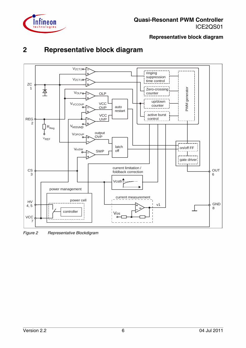
2 Representative block diagram
Figure 2 Representative Blockdigram
GND8
CS3
REG2
OUT6
ZC1
controller Vos
OLP
VCCOVP
VCCUVP
outputOVP
current limitation /foldback correction
V
V
V
V
autorestart
latchoff
current measurement
V
SWP
VREF
R
ZCT2
VCCOVP
vccuvp
OPOVP
csSW
v1
power management
Reg
Vcsth
on/off FF
gate driver
PW
Mgenera
tor
Zero-crossingcounter
up/downcounter
HV4, 5
VCC7
power cell
VOLP
active burstcontrol
ringingsuppressiontime controlVZCT1

Quasi-Resonant PWM ControllerICE2QS01
Functional Description
Version 2.2 7 4 Jul 2011
3 Functional Description
3.1 VCC Pre-Charging and TypicalVCC Voltage During Start-up
In the controller ICE2QS01, a power cell is integrated.As shown in Figure 2, the power cell consists of a highvoltage device and a controller, whereby the highvoltage device is controlled by the controller. Thepower cell provides a pre-charging of the VCCcapacitor till VCC voltage reaches the VCC turned-onthreshold VVCCon and the IC begins to operate, while itmay keep the VCC voltage at a constant value duringburst mode operation when the output voltage is pulleddown or the power from the auxiliary winding is notenough, or when the IC is latched off in certainprotection mode.
Once the mains input voltage is applied, a rectifiedvoltage shows across the capacitor Cbus. The highvoltage device provides a current to charge the VCCcapacitor Cvcc. Before the VCC voltage reaches acertain value, the amplitude of the current through thehigh voltage device is only determined by its channelresistance and can be as high as several mA. After theVCC voltage is high enough, the controller controls thehigh voltage device so that a constant current around1mA is provided to charge the VCC capacitor further,until the VCC voltage exceeds the turned-on thresholdVVCCon. As shown as the time phase I in Figure 3, theVCC voltage increase near linearly.
Figure 3 VCC voltage at start up
The time taking for the VCC pre-charging can then beapproximately calculated as:
[1]
where IVCCcharge2 is the charging current from the powercell which is 1.05mA, typically.
Exceeds the VCC voltage the turned-on thresholdVVCCon of at time t1, the power cell is switched off, andthe IC begins to operate with a soft-start. Due to powerconsumption of the IC and the fact that still no energyfrom the auxiliary winding to charge the VCC capacitorbefore the output voltage is built up, the VCC voltage
drops (Phase II). Once the output voltage is highenough, the VCC capacitor receives then energy fromthe auxiliary winding from the time point t2 on. The VCCthen will reach a constant value depending on outputload.
Since there is a VCC undervoltage protection, thecapacitance of the VCC capacitor should be selected tobe high enough to ensure that enough energy is storedin the VCC capacitor so that the VCC voltage will nevertouch the VCC under voltage protection thresholdVVCCUVP before the output voltage is built up. Therefore,the capacitance should fulfill the following requirement:
[2]
with IVCCop the operating current of the controller.
3.2 Soft-start
At the time t1, the IC begins to operate with a soft-start.By this soft-start the switching stresses for the switch,diode and transformer are minimised. The soft-startimplemented in the ICE2QS01 is a digital time-basedfunction. The preset soft-start time is 24ms with 8steps. The internal reference for the regulation voltagebegins at 1.35V and with an increment of 0.35V foreach following step.
3.3 Normal Operation
The PWM section of the IC can be divided into twomain portions: PWM controller for normal operationand PWM controller for burst mode operation. ThePWM controller for normal operation will be describedin the following paragraphs, while the PWM controllerfor burst mode operation will be discussed in the nextsection.
The PWM controller for normal operation consists ofdigital signal processing circuit including an up/downcounter, a zero-crossing counter (ZC-counter) and acomparator, and analog circuit including a currentmeasurement unit and a comparator. The switch-onand -off time point is determined by the digital circuitand the analog circuit, respectively. As inputinformation for the switch-on determination, the zero-crossing input signal and the value of the up/downcounter are needed, while the feedback signal vREG
and the current sensing signal vCS are necessary forthe switch-off determination. Details about theoperation of the PWM controller in normal operationare illustrated in the following paragraphs.
3.3.1 Switch-on Determination
As mentioned above, the digital signal processingcircuit consists of an up/down counter, a zero-crossingcounter and a comparator. A ringing suppression time
VVCCon
VCC
VVCCUVP
t1 tt2
i ii iii
t1
VVCCon Cvcc×
IVCCch e2arg----------------------------------=
Cvcc
IVCCop t2 t1–( )×
VVCCon VVCCUVP–------------------------------------------------³
Quasi-Resonant PWM ControllerICE2QS01
Functional Description
Version 2.2 8 4 Jul 2011
controller is implemented to avoid mistriggering by thering after MOSFET is turned off. Functionality of theseparts is described as in the following.
3.3.1.1 Up/down Counter
The up/down counter stores the number of zerocrossing to be ignored before the main power switch isswitched on after demagnetisation of the transformer.This value is a function of the regulation voltage, whichcontains information about the output power.Generally, a high output power results in a highregulation voltage. According to this information, thevalue in the up/down counter is changed to a low valuein case of high regulation voltage, and to a high valuein case of low regulation voltage. In ICE2QS01, thelowest value of the counter is 1 and the highest 7.Following text explains how the up/down counter valuechanges in responding to the regulation voltage vREG.The regulation voltage vREG is internally compared withthree thresholds VRL, VRH and VRM. According to theresults, the value in the up/down counter is changed,which is summarised in Table 1 and Figure 4respectively.
Table 1 Operation of the up/down counter
Figure 4 Up/down counter operation
According to the comparison results the up/downcounter counts upwards, keeps unchanged or countsdownwards. However, the value in up/down counter is
limited between 1 and 7. If the counter tends to countbeyond this range, the attempt is ignored.
In normal case, the up/down counter can only bechanged by one each time at the clock period of 48ms.However, to ensure a fast response to sudden loadincrease, the counter is set to 1 in the followingswitching period after the regulation voltage vREG
exceeds the threshold VRM.
3.3.1.2 Zero-Crossing Counter and RingingSuppression Time Controller
In the system, the voltage from the auxiliary winding isapplied to the zero-crossing pin through a RC network,which provides a time delay to the voltage from theauxiliary winding. Internally, this pin is connected to aclamping network, a zero-crossing detector, an outputovervoltage (OP OVP) detector and a ringingsuppression time controller.
During on-state of the power switch a negative voltageapplies to the ZC pin. Through the internal clampingnetwork, the voltage at the pin is clamped to certainlevel. However, it is highly recommended that a fast-recovery diode Dzc is added to block the negativevoltage when the power switch is on. This is becausethe device in MOS technology is sensitive to negativevoltage.
The voltage at the ZC pin vZC is compared with thethreshold VZCT1. Once the voltage vZC crosses thethreshold at its falling edge, a pulse is generated whichis fed to the zero-crossing counter and the countervalue increases by 1.
After MOSFET is turned on, there will be someoscillation on VDS, which will also appear on the voltageon ZC pin. To avoid the MOSFET is turned onmistriggerred by such oscillation, a ringing suppressiontimer is implemented. The time is dependent on thevoltage vZC. When the voltage vZC is lower than thethreshold VZCT2, a longer preset time applies, while ashorter time is set when the voltage vZC is higher thanthe threshold.
The voltage vZC is used for the output overvoltageprotection, as well. Once the voltage at this pin ishigher than the threshold VOPOVP during off-time of themain switch, the IC is latched off after a fixed blankingtime.
To achieve the switch-on at voltage valley, the voltagefrom the auxiliary winding is fed to a time delay network(the RC network consists of Dzc, Rzc1, Rzc2 and Czc asshown in typical application circuit) before it is appliedto the zero-crossing detector through the ZC pin. Theneeded time delay to the main oscillation signal Dtshould be approximately one fourth of the oscillationperiod (by transformer primary inductor and drain-source capacitor) minus the propagation delay from the
vREGup/down counteraction
Always lower than VRLCount upwards till7
Once higher than VRL, butalways lower than VRH
Stop counting, novalue changing
Once higher than VRH, butalways lower than VRM
Count downwardstill 1
Once higher than VRMSet up/downcounter to 1
1Case 3
Case 2
Case 1
n n+
1
n+
2
n+
2
n+
2
n+
2
n+
1
n n-1
4 5 6 6 6 6 5 4 3
1
1
2 3 4 4 4 4 3 2 1
7 7 7 7 7 7 6 5 4
t
tV
FB
VRM
VRH
VRL
clock T=48ms
1

Quasi-Resonant PWM ControllerICE2QS01
Functional Description
Version 2.2 9 4 Jul 2011
detected zero-crossing to the switch-on of the mainswitch tdelay, theoretically:
[3]
This time delay should be matched by adjusting thetime constant of the RC network which is calculated as:
[4]
3.3.1.3 Switch-on Determination
In the system, turn-on of the power switch depends onthe value of the up/down counter, the value of the zero-crossing counter and the voltage at the ZC pin vZC.Turn-on happens only when the value in the bothcounters are the same and the voltage at the ZC islower than the threshold VZCT1. For comparison of thevalues from both counters, a digital comparator is used.Once these counters have the same value, thecomparator generates a signal which sets the on/offflip-flop, only when the voltage vZC is lower than thethreshold VZCT1.
Another signal which may trigger the digital comparatoris the output of a TsMax clock signal, which limits themaximum off time to avoid the low-frequencyoperation.
During active burst mode operation, the digitalcomparator is disabled and no pulse will be generated.
3.3.2 Switch-off Determination
In the converter system, the primary current is sensedby an external shunt resistor, which is connectedbetween low-side terminal of the main power switchand the common ground. The sensed voltage acrossthe shunt resistor vCS is applied to an internal currentmeasurement unit, and its output voltage v1 iscompared with the regulation voltage vreg. Once thevoltage v1 exceeds the voltage vREG, the output flip-flopis reset. As a result, the main power switch is switchedoff. The relationship between the v1 and the vcs isdescribed by:
[5]
To avoid mistriggering caused by the voltage spikeacross the shunt resistor after switch-on of the mainpower switch, a 330ns leading edge blanking timeapplies to output of the comparator.
3.3.3 Foldback Point Correction
In addition to the cycle-by-cylce primary currentlimitation, the IC incorporats a foldback pointcorrection. The current limit on CS pin voltage is now atime dependent one. If the mains input voltage is high,the MOSFET on time will be short and the current limitwill be low. In such a way, the maximum output powerfor the SMPS designed with ICE2QS01 will be nearlyconstant against the variations of mains input voltage.The current sense voltage limit versus the MOSFETmaximum on time is shown in Figure 5.
DtTosc
4---------- tdelay–=
ttd Czc
Rzc1 Rzc2×
Rzc1 Rzc2+----------------------------×=
v1 3.3 vCS× 0.7+=
Figure 5 Maximum current limit versus MOSFET maximum on time
0
0.2
0.4
0.6
0.8
1
0 5 10 15 20 25 30
Ton(us)
Vc
s-m
ax
(V)
Quasi-Resonant PWM ControllerICE2QS01
Functional Description
Version 2.2 10 4 Jul 2011
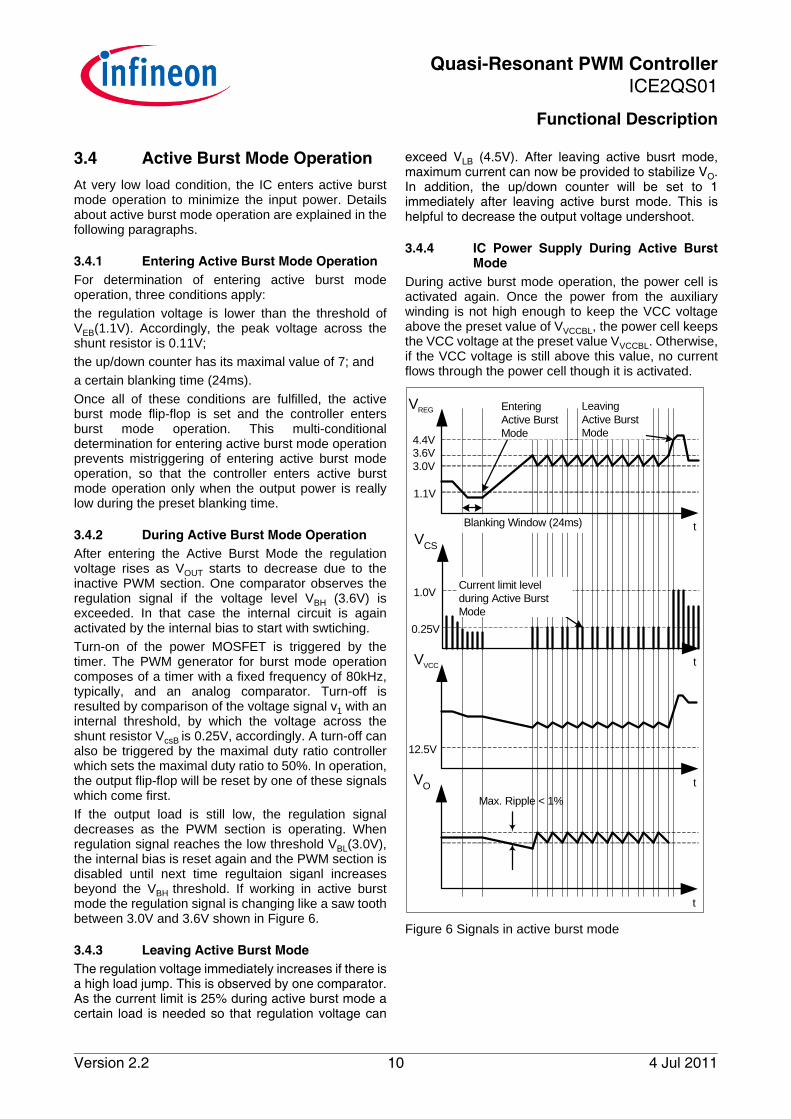
3.4 Active Burst Mode Operation
At very low load condition, the IC enters active burstmode operation to minimize the input power. Detailsabout active burst mode operation are explained in thefollowing paragraphs.
3.4.1 Entering Active Burst Mode Operation
For determination of entering active burst modeoperation, three conditions apply:
the regulation voltage is lower than the threshold ofVEB(1.1V). Accordingly, the peak voltage across theshunt resistor is 0.11V;
the up/down counter has its maximal value of 7; and
a certain blanking time (24ms).
Once all of these conditions are fulfilled, the activeburst mode flip-flop is set and the controller entersburst mode operation. This multi-conditionaldetermination for entering active burst mode operationprevents mistriggering of entering active burst modeoperation, so that the controller enters active burstmode operation only when the output power is reallylow during the preset blanking time.
3.4.2 During Active Burst Mode Operation
After entering the Active Burst Mode the regulationvoltage rises as VOUT starts to decrease due to theinactive PWM section. One comparator observes theregulation signal if the voltage level VBH (3.6V) isexceeded. In that case the internal circuit is againactivated by the internal bias to start with swtiching.
Turn-on of the power MOSFET is triggered by thetimer. The PWM generator for burst mode operationcomposes of a timer with a fixed frequency of 80kHz,typically, and an analog comparator. Turn-off isresulted by comparison of the voltage signal v1 with aninternal threshold, by which the voltage across theshunt resistor VcsB is 0.25V, accordingly. A turn-off canalso be triggered by the maximal duty ratio controllerwhich sets the maximal duty ratio to 50%. In operation,the output flip-flop will be reset by one of these signalswhich come first.
If the output load is still low, the regulation signaldecreases as the PWM section is operating. Whenregulation signal reaches the low threshold VBL(3.0V),the internal bias is reset again and the PWM section isdisabled until next time regultaion siganl increasesbeyond the VBH threshold. If working in active burstmode the regulation signal is changing like a saw toothbetween 3.0V and 3.6V shown in Figure 6.
3.4.3 Leaving Active Burst Mode
The regulation voltage immediately increases if there isa high load jump. This is observed by one comparator.As the current limit is 25% during active burst mode acertain load is needed so that regulation voltage can
exceed VLB (4.5V). After leaving active busrt mode,maximum current can now be provided to stabilize VO.In addition, the up/down counter will be set to 1immediately after leaving active burst mode. This ishelpful to decrease the output voltage undershoot.
3.4.4 IC Power Supply During Active BurstMode
During active burst mode operation, the power cell isactivated again. Once the power from the auxiliarywinding is not high enough to keep the VCC voltageabove the preset value of VVCCBL, the power cell keepsthe VCC voltage at the preset value VVCCBL. Otherwise,if the VCC voltage is still above this value, no currentflows through the power cell though it is activated.
Figure 6 Signals in active burst mode
1.1V
3.6V4.4V
VREG
t
0.25V
1.0V
VCS
12.5V
VVCC t
tVO
t
3.0V
Max. Ripple < 1%
Blanking Window (24ms)
Current limit levelduring Active BurstMode
LeavingActive BurstMode
EnteringActive BurstMode

Quasi-Resonant PWM ControllerICE2QS01
Functional Description
Version 2.2 11 4 Jul 2011
3.5 Protection Functions
The IC provides full protection functions. The followingtable summarizes these protection functions.
Table 2 Protection features
During operation, the VCC voltage is continuouslymonitored. In case of an under- or an over-voltage, theIC is reset and the main power switch is then kept off.After the VCC voltage falls below the thresholdVVCCUVP, the power cell is activated. The VCC capacitoris then charged up. Once the voltage exceeds thethreshold VVCCon, the IC begins to operate with a newsoft-start.
In case of open control loop or output over load, theregulation voltage will be pulled up . After a blankingtime of 24ms, the IC enters auto-restart mode. Theblanking time here enables the converter to provide ahigh power in case the increase in VREG is due to asudden load increase. During off-time of the powerswitch, the voltage at the zero-crossing pin ismonitored for output over-voltage detection. If thevoltage is higher than the preset threshold vOPOVP, theIC is latched off after the preset blanking time.
If the voltage at the current sensing pin is higher thanthe preset threshold vcsSW during on-time of the powerswitch, the IC is latched off. This is short-windingprotection.
During latch-off protection mode, the power cell isactivated and it keeps the VCC voltage at the level ofVVCCBL.
VCC Overvoltage Auto Restart Mode
VCC Undervoltage Auto Restart Mode
Overload/Open Loop Auto Restart Mode
Output Overvoltage Latched Off Mode
Short Winding Latched Off Mode

Quasi-Resonant PWM ControllerICE2QS01
Electrical Characteristics
Version 2.2 12 4 Jul 2011
4 Electrical Characteristics
Note: All voltages are measured with respect to ground (Pin 8). The voltage levels are valid if other ratings arenot violated.
4.1 Absolute Maximum Ratings
Note: Absolute maximum ratings are defined as ratings, which when being exceeded may lead to destructionof the integrated circuit. For the same reason make sure, that any capacitor that will be connected to pin 7(VCC) is discharged before assembling the application circuit.
4.2 Operating Range
Note: Within the operating range the IC operates as described in the functional description.
Parameter Symbol Limit Values Unit Remarks
min. max.
HV Voltage VHV - 500 V
VCC Supply Voltage VVCC -0.3 27 V
REG Voltage VREG -0.3 5.0 V
ZC Voltage VZC -0.3 5.0 V
CS Voltage VCS -0.3 5.0 V
OUT Voltage VOUT -0.3 27 V
Junction Temperature Tj -40 125 °C
Storage Temperature TS -55 150 °C
Thermal ResistanceJunction-Ambient
RthJA - 90 K/W PG-DIP-8
ESD Capability VESD - 2 kV Human body model1)
1) According to EIA/JESD22-A114-B (discharging a 100pF capacitor through a 1.5kW series resistor)
Parameter Symbol Limit Values Unit Remarks
min. max.
VCC Supply Voltage VVCC VVCCUVP VVCCOVP V
Junction Temperature TjCon -25 125 °C

Quasi-Resonant PWM ControllerICE2QS01
Electrical Characteristics
Version 2.2 13 4 Jul 2011
4.3 Characteristics
4.3.1 Supply Section
Note: The electrical characteristics involve the spread of values guaranteed within the specified supply voltageand junction temperature range TJ from – 25 oC to 125oC. Typical values represent the median values,which are related to 25°C. If not otherwise stated, a supply voltage of VCC = 18 V is assumed.
Parameter Symbol Limit Values Unit Test Condition
min. typ. max.
Start-Up Current IVCCstart - 300 550 mA VVCC = 21V
VCC Charge Current IVCCcharge1 - - 5.0 mA VVCC = 0V
IVCCcharge2 0.55 1.05 1.60 mA VVCC = 1V
IVCCcharge3 - 0.88 - mA VVCC = 21V
Leakage Current ofPower Cell
IStartLeak - 0.2 50 mA VHV= 610Vat Tj = 100°C
Supply Current in normaloperation
IVCCop - 2.5 3.6 mA Output low
Supply Current inAuto Restart Modewith Inactive Gate
IVCCrestart - 300 - mA
Supply Current inLatch-off Mode
IVCClatch - 300 - mA
Supply Current in Burst Modewith Inactive Gate
IVCCburst - 500 950 mA VREG = 2.5V
Supply Voltage with no powerfrom auxiliary winding in burstmode or in latch-off mode
VVCCBL - 12.5 - V VHV = 100V
VCC Turn-On Threshold VVCCon 21.2 22.0 22.8 V
Internal Reference Voltage VREF 4.8 5.0 5.2 V measured at pin REG,IREG = 0

Quasi-Resonant PWM ControllerICE2QS01
Electrical Characteristics
Version 2.2 14 04 Jul 2011
4.3.2 PWM Section
Parameter Symbol Limit Values Unit Test Condition
min. typ. max.
Regulation Pull-Up Resistor RREG 14 23 33 kW
PWM-OP Gain AV 3.18 3.3 - -
Offset for Voltage Ramp VOS 0.63 0.7 - V
Soft-Start time tSOFTS 18 21 38 ms
Zero crossing threshold voltage VZCT1 20 50 110 mV
Ringing suppression threshold VZCT2 0.7 V
Minimum ringing suppressiontime
tZCRST1 2.2 4.2 5.5 ms VZC > VZCT2
Maximum ringing suppressiontime
tZCRST2 - 42 - ms VZC < VZCT2
Threshold to set Up/DownCounter to one
VRM - 3.9 - V
Threshold for downwardcounting
VRH - 3.2 - V
Threshold for upward counting VRL - 2.5 - V
Counter time1) tCOUNT - 48 - ms
Maximum restart time in normaloperation
tsMax 33 42 60 ms VZC<VZCT1
Leading Edge Blanking tLEB 200 330 460 ns
Peak current limitation in normaloperation
Vcsth 0.95 1.0 1.05 V
Regulation voltage for enteringBurst Mode
VEB - 1.1 - V
Regulation voltage for leavingBurst Mode
VLB - 4.5 - V
Regulation voltage for burst-on VBH - 3.6 - V
Regulation voltage for burst-off VBL - 3.0 - V
Fixed Switching Frequency inBurst Mode
fsB 64 80 96 kHz
Max. Duty Cycle in Burst Mode DmaxB - 0.5 -
Peak Current Limitation in BurstMode
VcsB 0.22 0.25 0.3 V
1) The parameter is not subject to production test - verified by design/characterization

Quasi-Resonant PWM ControllerICE2QS01
Electrical Characteristics
Version 2.2 15 4 Jul 2011
4.3.3 Protection
Note: The trend of all the voltage levels in the Control Unit is the same regarding the deviation except VVCCOVP
4.3.4 Gate Driver
Parameter Symbol Limit Values Unit Test Condition
min. typ. max.
VCC overvoltage threshold VVCCOVP 24 25.0 26 V
VCC undervoltage threshold VVCCUVP 10.3 11.0 11.7 V
Over Load or Open LoopDetection threshold for OLPprotection at REG pin
VOLP - 4.5 - V
Over Load or Open LoopProtection Blanking Time
TOLP-B 16 24 35 ms
Output Overvoltage detectionthreshold at the ZC pin
VOPOVP - 4.5 - V
Threshold for short windingprotection
VcsSW - 1.68 - V
Parameter Symbol Limit Values Unit Test Condition
min. typ. max.
Output voltage at logic low VGATElow - 0.7 - V IOUT = 20mA
Output voltage at logic high VGATEhigh - 10.0 - V IOUT = -20mA
Output voltage active shut down VGATEasd - 1.0 - VV
VVCC = 7VIOUT = 20mA
Rise Time trise - 100 - ns COUT = 4.7nF
Fall Time tfall - 25 - ns COUT = 4.7nF

Quasi-Resonant PWM ControllerICE2QS01
Outline Dimension
Version 2.2 16 04 Jul 2011
5 Outline Dimension
Figure 7 PG-DIP-8
PG-DIP-8(Leadfree Plastic Dual In-Line)

Qualität hat für uns eine umfassendeBedeutung. Wir wollen allen IhrenAnsprüchen in der bestmöglichenWeise gerecht werden. Es geht uns alsonicht nur um die Produktqualität –unsere Anstrengungen geltengleichermaßen der Lieferqualität undLogistik, dem Service und Supportsowie allen sonstigen Beratungs- undBetreuungsleistungen.
Dazu gehört eine bestimmteGeisteshaltung unserer Mitarbeiter.Total Quality im Denken und Handelngegenüber Kollegen, Lieferanten undIhnen, unserem Kunden. UnsereLeitlinie ist jede Aufgabe mit „NullFehlern“ zu lösen – in offenerSichtweise auch über den eigenenArbeitsplatz hinaus – und uns ständigzu verbessern.
Unternehmensweit orientieren wir unsdabei auch an „top“ (Time OptimizedProcesses), um Ihnen durch größereSchnelligkeit den entscheidendenWettbewerbsvorsprung zu verschaffen.
Geben Sie uns die Chance, hoheLeistung durch umfassende Qualität zubeweisen.
Wir werden Sie überzeugen.
Quality takes on an allencompassingsignificance at Semiconductor Group.For us it means living up to each andevery one of your demands in the bestpossible way. So we are not onlyconcerned with product quality. Wedirect our efforts equally at quality ofsupply and logistics, service andsupport, as well as all the other ways inwhich we advise and attend to you.
Part of this is the very special attitude ofour staff. Total Quality in thought anddeed, towards co-workers, suppliersand you, our customer. Our guideline is“do everything with zero defects”, in anopen manner that is demonstratedbeyond your immediate workplace, andto constantly improve.
Throughout the corporation we alsothink in terms of Time OptimizedProcesses (top), greater speed on ourpart to give you that decisivecompetitive edge.
Give us the chance to prove the best ofperformance through the best of quality– you will be convinced.
h t t p : / / w w w . i n f i n e o n . c o m
Total Quality Management
Published by Infineon Technologies AG


