VISHAY SILICONIX Power MOSFETs Application Note 833 Switching Analysis of Synchronous Rectifier MOSFETs With Phase-Shifted Full-Bridge Converter and Current Doubler APPLICATION NOTE Document Number: 69747 www.vishay.com Revision: 11-Oct-07 1 By Patrick Chiang and Mark Hu Abstract This application note will analyze the switching behavior of synchronous rectifier MOSFETs in a phase-shifted full-bridge converter topology with a current doubler. Figure 1 shows the basic circuit of this application. An overview will describe the timing diagram of a phase-shifted full-bridge converter for achieving zero voltage switching (ZVS). Two topologies are introduced for gate driving of synchronous rectifier (SR) MOSFETs. The timing diagrams will introduce the SR MOSFET operations during every stage for both topologies. The body diode will be highlighted, and the operational phenomena that occur when the SR MOSFET turns off will be described. The power dissipation of SR MOSFETs will be presented as equations to assist in designs, while test results of waveforms will help in understanding the application. A summary will include the advantages of SR MOSFETs, an efficiency comparison, and other design considerations. Figure 1 - Phase-Shifted Full-Bridge Converter Introduction to the Phase-Shifted Full-Bridge Converter The phase-shifted full-bridge converter has long been used to achieve high efficiency and high density in power supply designs with outputs from 500 W to 5000 W. The traditional full-bridge converter transfers power from primary bulk capacitors to secondary LC filters when its MOSFETs (QA and QD, or QB and QC) are turned on at the same time. This operation results in increased power dissipation (known as switching loss) when a primary MOSFET is turned on and off. The higher the switching frequency, the greater the switching losses. The phase-shifted full-bridge converter introduces an almost 50 % fixed-duty cycle to QA, QB, QC, and QD. The pulse width modulation (PWM) duty is controlled by the overlapped duty of QA and QD, and QB and QC. There is a small amount of overlap between QA and QB, and QC and QD, which is called PWM delay (PWM delay AB, and PWM delay CD). PWM delay will prevent the same-side MOSFETs (QA and QB, or QC and QD) from turning on simultaneously, which would result in a short circuit that burns out the MOSFETs. In addition, the delay time helps the MOSFETs to achieve zero voltage switching (ZVS). When the PWM pulse is off, the snubber inductance Lr, by way of storage energy, will resonate with the output capacitances of the MOSFETs and oscillate the MOSFET voltage to zero before the MOSFETs turn on at the next period. At this stage, ZVS (which means no switching loss) occurs and a significant improvement in efficiency is gained. Due to high density (per W/inch 3 ) and thermal considerations, most designers do not add an external snubber inductor in conjunction with the transformer (shown in Figure 1). The snubber inductance Lr results from the leakage inductance of transformer T1. Only if the primary current Ip is enough to let Lr be stored at a minimum energy, and an achieved ZVS transition, is the external inductor not necessary. Using the leakage inductance of the transformer, most power supplies can achieve ZVS with more than 50 % maximum load. It is necessary to add Cb to avoid an unbalance of the transformer flux and saturation of the transformer. SA SC SB SD T1 + - Vi SR1 SR2 L2 L1 C 0 + - VT QB QD QC QA Q1 Q2 + - Lr Cb
Transcript
V I S H A Y S I L I C O N I X
Power MOSFETs Application Note 833
Switching Analysis of Synchronous Rectifier MOSFETs With Phase-Shifted Full-Bridge Converter and Current Doubler
AbstractThis application note will analyze the switching behavior ofsynchronous rectifier MOSFETs in a phase-shiftedfull-bridge converter topology with a current doubler.Figure 1 shows the basic circuit of this application. Anoverview will describe the timing diagram of aphase-shifted full-bridge converter for achieving zerovoltage switching (ZVS). Two topologies are introduced forgate driving of synchronous rectifier (SR) MOSFETs. Thetiming diagrams will introduce the SR MOSFET operationsduring every stage for both topologies. The body diode willbe highlighted, and the operational phenomena that occurwhen the SR MOSFET turns off will be described. Thepower dissipation of SR MOSFETs will be presented asequations to assist in designs, while test results ofwaveforms will help in understanding the application. A
summary will include the advantages of SR MOSFETs, anefficiency comparison, and other design considerations.
Figure 1 - Phase-Shifted Full-Bridge Converter
Introduction to the Phase-Shifted Full-Bridge ConverterThe phase-shifted full-bridge converter has long been usedto achieve high efficiency and high density in power supplydesigns with outputs from 500 W to 5000 W. The traditionalfull-bridge converter transfers power from primary bulkcapacitors to secondary LC filters when its MOSFETs (QAand QD, or QB and QC) are turned on at the same time. Thisoperation results in increased power dissipation (known asswitching loss) when a primary MOSFET is turned on andoff. The higher the switching frequency, the greater theswitching losses.
The phase-shifted full-bridge converter introduces analmost 50 % fixed-duty cycle to QA, QB, QC, and QD. Thepulse width modulation (PWM) duty is controlled by theoverlapped duty of QA and QD, and QB and QC. There is asmall amount of overlap between QA and QB, and QC andQD, which is called PWM delay (PWM delay AB, andPWM delay CD). PWM delay will prevent the same-sideMOSFETs (QA and QB, or QC and QD) from turning onsimultaneously, which would result in a short circuit thatburns out the MOSFETs. In addition, the delay time helps
the MOSFETs to achieve zero voltage switching (ZVS).When the PWM pulse is off, the snubber inductance Lr, byway of storage energy, will resonate with the outputcapacitances of the MOSFETs and oscillate the MOSFETvoltage to zero before the MOSFETs turn on at the nextperiod. At this stage, ZVS (which means no switching loss)occurs and a significant improvement in efficiency isgained.
Due to high density (per W/inch3) and thermalconsiderations, most designers do not add an externalsnubber inductor in conjunction with the transformer(shown in Figure 1). The snubber inductance Lr results fromthe leakage inductance of transformer T1. Only if theprimary current Ip is enough to let Lr be stored at aminimum energy, and an achieved ZVS transition, is theexternal inductor not necessary. Using the leakageinductance of the transformer, most power supplies canachieve ZVS with more than 50 % maximum load. It isnecessary to add Cb to avoid an unbalance of thetransformer flux and saturation of the transformer.
SA SC
SB SD
T1
+
-
Vi
SR1
SR2
L2
L1
C0
+
-VT
QB QD
QCQA Q1
Q2
+
-
Lr
Cb
Switching Analysis of Synchronous Rectifier MOSFETs With Phase-Shifted Full-Bridge Converter and Current Doubler
if Cxfrm is small and negligible with comparison to COSS,
.
Designers may measure the IDS and VDS of a MOSFET tofind out at which output load ZVS of the MOSFET startsto happen (for example, 40 %). If Lr is the leakageinductance of the transformer, the LCR meter can measureLr by shorting the secondary wire. Adequate Ip stores theenergy and, by way of Lr, forces the VDS of the MOSFETto zero before the MOSFET turns on.
In Figures 2 and 3, the primary current is Ip and a > b > c.The critical point is Ip = b. That is
If Ip ≥ b, the MOSFET can achieve ZVS. If Ip < b, ZVS isnot possible.
Figure 2 - COSS Discharging Waveform
Figure 3 - COSS Charging Waveform
• The second criterion for achieving ZVS is that the delaytime is long enough to allow resonant voltages to finishthe energy transfer in COSS and Lr. Assuming thefrequency of the resonant is Fr, one period time Tr is .
Figures 2 and 3 show the voltage waveforms of theresonant transitions. Figure 2 occurs while the COSS of theMOSFET discharges from Vi = max to zero. Figure 3occurs while the COSS of the MOSFET charges fromVi = zero to max. The boundary condition occurs whenIp = b. The delay time must be equal to or greater than tb,or the MOSFET cannot achieve ZVS. Designers maychoose to let the delay time be equal to ta, and have noZVS in light loads. The criteria of the duty cycle isDutymaximum + Dutydelay = 50 % switching period.
The larger delay time will cause the maximum duty cycleto be smaller, impacting the hold-up time performance.
The power transition from Lr to COSS needs to becompleted to achieve ZVS. The minimum time isone-fourth of the resonant period.
12--- Lr Ip2 1
2--- Cr Vi2××>××
Cr 83--- COSS×⎝ ⎠⎛ ⎞ Cxfm+=
Cr 83--- COSS×⎝ ⎠⎛ ⎞=
12--- Lr Ip2 4
3--- COSS Vi2××>××⇒
12--- Lr× b2× 4
3--- COSS× Vi, max2 b⇒× 8
3---
COSS Vi, max2×Lr
-------------------------------------------×= =
Vi = max
Vi = 0
Ip = b
Ip = a
Ip = c
ta
tb
ZVS Point
Vi = max
Vi = 0
Ip = b
Ip = a
Ip = c
ta
tb
ZVS Point
1Fr------
tb 14--- Tr×=⇒
Tr 1Fr------ , Fr 1
2 π× Lr Cr××------------------------------------------==⇒
tb π2--- Lr Cr××=⇒
Switching Analysis of Synchronous Rectifier MOSFETs With Phase-Shifted Full-Bridge Converter and Current Doubler
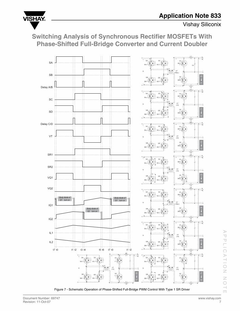
Schematic Operation and Description• Timeframe t0 → t1:
At the beginning of this timeframe, QD has already turnedon and the VDS of QA is zero. QA starts to turn on whenthe VDS equals zero. The primary current is flowingthrough QA, T1, and QD as shown in Figure 4. The powertransfers from the Vi source tank to the VT of thesecondary PWM pulse source by way of transformer T1.
• Timeframe t1 → t2:Inductance Lr exists inside of transformer T1. Thecharacteristics of inductance will keep the current Ip in thesame direction. If there is no passive component in thecurrent loop of Ip, the value of Ip will remain the samewith no energy loss. At t1, QD turns off. The stored energyof Lr forces Ip to keep flowing with its value at t1. Thisaction will start to charge the COSS of QD and dischargethe COSS of QC as shown in Figure 4. If the Ip is adequateas shown in Figure 4, the voltage of drain of QD, or sourceof QC, will resonate from Vi, max to zero. The ZVStransition will finish within one-fourth of the resonantcycle. After the voltage of drain of QD, or source of QC,reaches zero, the current Ip stops flowing through theCOSS. It turns on the body diode of QC and Ip keepsflowing.
• Timeframe t2 → t3:At t2, QC starts to turn on. Ip transfers the current pathfrom the body diode of QC to the MOSFET QC. As shownin Figure 4, the Ip current will keep flowing through QA,T1, and QC with almost the same value, which means theresistance loss is very low.
• Timeframe t3 → t4:At t3, QA turns off. The stored energy of Lr forces Ip tokeep flowing with its value at t3. This action will start tocharge the COSS of QA and discharge the COSS of QB asshown in Figure 4. If the Ip is adequate as shown in Figure4, the voltage of source of QA, or drain of QB, willresonate from Vi, max to zero. The ZVS transition willfinish within one-fourth of the resonant cycle. After thevoltage of source of QA, or drain of QB, reaches Vi, max,the current Ip stops flowing through the COSS. It turns onthe body diode of QB and keeps flowing.
• Timeframe t4 → t5:QC has already turned on and the VDS of QB is zero. QBstarts to turn on when its VDS is zero. The primary currentis flowing through QA, T1, and QD as shown in Figure 4.The power transfers from the Vi source tank to the VT ofthe secondary PWM pulse source by way of transformerT1.
• Timeframe t5 → t6:Inductance Lr exists inside of transformer T1. Thecharacteristics of inductance will keep the current Ip in thesame direction. If there is no passive component in thecurrent loop of Ip, the value of Ip will remain the same. Att1, QC turns off. The stored energy of Lr forces Ip to keepflowing with its value at t5. This action will start to chargethe COSS of QC and discharge the COSS of QD as shown inFigure 4. If the Ip is adequate as shown in Figure 4, thevoltage of drain of QD, or the source of QC, will resonatefrom Vi, max to zero. The ZVS transition will finishwithin one-fourth of the resonant cycle. After the voltageof drain of QD, or the source of QC, reaches zero, thecurrent Ip stops flowing through the COSS. It turns on thebody diode of QD and Ip keeps flowing.
• Timeframe t6 → t7:At t6, QD starts to turn on. Ip transfers the current pathfrom the body diode of QD to the MOSFET QD. Asshown in Figure 4, the Ip current will keep flowingthrough QB, T1, and QD with almost the same value,which means the resistance loss is very low.
• Timeframe t7 → t0:At t7, QB turns off. The stored energy of Lr forces Ip tokeep flowing with its value at t3. This action will start tocharge the COSS of QB and discharge the COSS of QA asshown in Figure 4. If the Ip is adequate as shown in Figure4, the voltage of drain of QB, or the source of QA, willresonate from zero to Vi, max. The ZVS transition willfinish within one-fourth of the resonant cycle. After thevoltage of drain of QB, or the source of QA, reaches Vimax, the current Ip stops flowing through the COSS. Itturns on the body diode of QA and keeps flowing.
Primary Circuit Application and Consideration:a. With adequate Ip, the primary MOSFETs of a
phase-shifted full-bridge converter switch will show nodissipation at the turn-on stage, i.e. ZVS. However, thepower dissipation at the turn-off stage cannot be avoided.
which refers to Figure 3.
Vi, a is the maximum voltage when Ip = a.
ωr 2 π× Fr, ta× , Ip a==
12--- Lr× a2× 4
3--- COSS× Vi, a2 Vi, a 3
8--- Lr a2×
COSS------------------×=⇒×=⇒
Switching Analysis of Synchronous Rectifier MOSFETs With Phase-Shifted Full-Bridge Converter and Current Doubler
To calculate ta is to find the time Vi, a(t) = Vi, max
Pat = power dissipation in the transition period.
The power dissipation of a MOSFET at turn-off is Pa, off (TSW is switching period).
If Ip=b, then
where
and
b. When the MOSFETs and the transformer start theresonant transition, energy is sometimes lost. The rDS(on),the forward drop voltage of the body diode, theparasitical resistance in the PCB, and the wire resistanceof the transformer gradually dissipate the energy storedas inductance. Some stored energy is dissipated in thetime interval of the C/D resonant transition delay and thePWM-off transition. The stored energy of the A/Bresonant transition delay will be smaller than that of theC/D resonant transition delay. Thus, it is easier to achieveZVS in the C/D resonant transition delay than the A/Bresonant transition delay. That is why the case thermaldata of MOSFETs QA and QB are always higher than QCand QD.
c. Thermal considerations in light loads are a problem.Phase-shifted control enlarges the overlap waveforms ofthe MOSFET voltage and current in light loads. Thatmeans power losses will increase tremendously in thissituation, because there is no ZVS and Ip keeps thevoltage of the MOSFET at a high value before switching.Even worse, most current power supplies specify smallerairflow under light output load conditions as a way ofreducing acoustic noise. The case temperature of theMOSFET will be very high. Designers should do thermaltesting around 10 % to 40 % of the load and check thedata carefully. Be sure to meet the de-rating guidelines ofthe customer's specifications. Designers may set avariable step value for delay A/B and delay C/D. Sensingthe primary current, the controller changes to a longerdelay time in light loads. The longer transition time canreduce the power losses in the MOSFET.
Vi, a ωr ta×( )sin× Vi, max tasin 1– Vi, max
Vi, a--------------------⎝ ⎠⎛ ⎞
ωr---------------------------------------=⇒=⇒
Pat 1ta----- Vi, a(t) Ip×( )dt 1
ta---- Vi, a ωsin t×( )× Ip×( )dt Vi, a a×
ta--------------------- ωrsin t×( )dt
0
ta
∫=0
ta
∫=0
ta
∫=⇒
Pat Vi, a a×ta ωr×
--------------------- 1 ωr ta×( )cos–( )× →=⇒
Pa, off taTSW----------- Vi, a a×
ta ωr×--------------------- 1 ωr ta×( )cos–( ) Pa, off1⇒××=⇒ Vi, a a×
Control Drivers of Synchronous Rectifier With Current Doubler
Figure 5 - Schematic Operation of Diode Rectifier
• The secondary side acts as a buck converter. The diodesact as switchers by following the power transferring fromthe primary side. When VT is positive, D1 willautomatically turn off. When VT is negative, D2 willautomatically turn off.
• Synchronous rectifiers can replace diode rectifiers. Thatis, control drivers of synchronous rectifiers behave asdiode rectifiers. Because the product of the averagecurrent Id and rDS(on) is much lower than the VF of the
diode, higher efficiency can be achieved by using the SRtopology. The SR MOSFET, however, must be controlledto turn on and perform in the zone of the diode turn-on asshown in Figure 5. If SR1 turns on before t1 and turns offafter t0, the sudden short circuit of Q1 and Q2 will resultin their burning out and damaging other components.
• Two types of control drivers have been introduced intoday's application.
Type 1 SR Driver• Designers may put the phase-shifted full-bridge controller
in the secondary side of the main transformer. In thisscenario, the control driver of the synchronous rectifier isbuilt up without an insulation transformer. See Figure 6.SR1 is controlled "off" in t1 and t2, and t7 and t0,providing a delay that avoids the short circuit of Q1 andQ2 and results in optimal efficiency.
Figure 6 - Schematic Diagram of Type 1 Synchronous Rectifier
SA SC
SB SD
T1
+
-
Vi
L2
L1
Co
+
-
VTQB QD
QCQA
D1
D2
+
-
Lr
Cb Ls
VT
t0t7 t1 t2 t3 t4 t5 t6 t7 t0 t1 t2
VD1
VD2
ID1
ID2
turn on
turn on
turn on
turn off
turn off
turn off
SA
SD
SR2
SB
SC
SR1
current driver
current driver
TRUTH TABLE OF TYPE 1 SYNCHONOUS RECTIFIER
STATEPRIMARY GATE SIGNAL SR INPUT SIGNAL
SA SB SC SD SR1 SR2t0 → t1 H L L H L Ht1 → t2 H L L L L Ht2 → t3 H L H L H Ht3 → t4 L L H L H Lt4 → t5 L H H L H Lt5 → t6 L H L L H Lt6 → t7 L H L H H Ht7 → t0 L L L H L H
Switching Analysis of Synchronous Rectifier MOSFETs With Phase-Shifted Full-Bridge Converter and Current Doubler
Schematic Operation and Description With Type 1 SR Driver
• Timeframe t0 → t1:QA and QD are turned on and power is transferred fromthe primary side to the secondary side. SR2 is alreadyturned on. No current flows through Q1. Q2 will take allthe transferring current flow through itself. However,before t0, the body diode of Q1 is turned on. At t0, forcingthe body diode of Q1 to turn off will cause a diodereverse-recovery condition. The high spike voltage of Q1VDS and the turn-off switching loss occur.Assuming output inductors (L1 and L2) both work incontinuous mode, the currents of L1 and L2 will keepflowing in the same direction. Two paths of current floware separated through L1 and L2. The current of L1 isincreasing by the forced voltage VT, and that of L2 isdecreasing with the freewheeling stored energy in L2.
• Timeframe t1 → t2:At t1, the forced voltage is off and transfers from themaximum value to zero voltage. In this short time, Q1 VDSwill reach zero voltage and the Q1 body diode will turn on.Since the primary Ip keeps almost the same value, thecurrent of the secondary side transformer is almost thesame value as at t1. Therefore, the current of body diodeQ1 will start at zero current and increase slowly. Besidesthe two current paths in the timeframe t0 → t1, the currentthrough the Q1 diode and L1 is the third path.
• Timeframe t2 → t3:At t2, SR1 starts to turn the Q1 MOSFET on. Because thebody diode of Q1 is already turned on, the VDS of Q1 iszero. ZVS occurs in the turn-on switching of Q1. Thethree current paths are the same as those of timeframet1 → t2. The third one, however, is not flowing throughthe Q1 diode, but the Q1 MOSFET.
• Timeframe t3 → t4:At t3, the voltage of QA source or QB source is resonatedfrom the maximum value to zero voltage. In this shorttime, the VDS of QB will reach zero voltage and the bodydiode will turn on. Since the primary IP keeps almost thesame value, the current of the secondary side transformeris almost the same value as at t1. Therefore, the currentof the body diode Q2 will take all the current of theQ2 MOSFET at t3. The three current paths are the same asthose of timeframe t2 → t3. However, the path throughMOSFET Q2 is changed through the body diode of Q2.
• Timeframe t4 → t5:QB and QC are turned on. SR2 is already turned on. Thereis no current flow through Q2. Q1 will take all thetransferring current flow through itself. However, beforet4, the body diode of Q2 is turned on. The high spikevoltage of Q1 VDS and the turn-off switching loss occur.Two paths of current flow are separated through L1 andL2. The current of L2 is increasing by forced voltage VT,and that of L1 is decreasing with the freewheeling storedenergy in L2.
• Timeframe t5 → t6:At t5, the forced voltage VT is off and transfers from themaximum value to zero voltage. In this short time, Q2 VDSwill reach zero voltage and the Q2 body diode will turn on.Since the primary IP keeps almost the same value, thecurrent of the secondary side transformer is almost thesame value as at t1. Therefore, the current of body diodeQ2 will start at zero current and increase slowly. Besidesthe two current paths in timeframe t4 → t5, the currentthrough the Q2 diode and L2 is the third path.
• Timeframe t6 → t7:At t6, SR2 starts to turn the Q2 MOSFET on. Because thebody diode of Q2 is already turned on, the VDS of Q2 iszero. ZVS occurs in the turn-on switching of Q2. Thethree current paths are the same as those of timeframet5 → t6. The third one, however, is not flowing throughthe Q2 diode, but the Q2 MOSFET.
• Timeframe t7 → t0:
At t7, the voltage of QA source or QB source is resonatedfrom the maximum value to zero voltage. In this shorttime, the VDS of QB will reach zero voltage and the bodydiode will turn on. Since the primary IP keeps almost thesame value, the current of the secondary side transformeris almost the same value as at t1. Therefore, the current ofbody diode Q1 will take all the current of the Q1 MOSFETat t7. The three current paths are the same as those oftimeframe t6 → t7. The path through the MOSFET Q1,however, is changed through the body diode of Q1.
Switching Analysis of Synchronous Rectifier MOSFETs With Phase-Shifted Full-Bridge Converter and Current Doubler
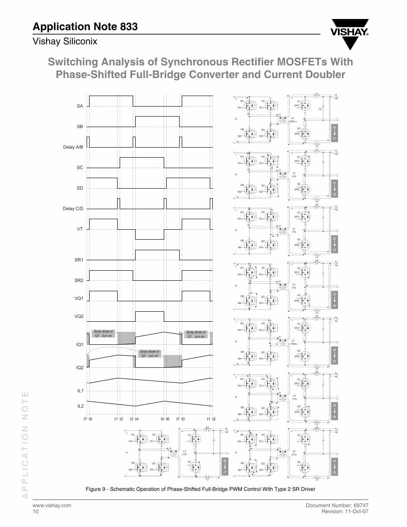
Type 2 SR Driver• The control driver of synchronous rectifier can use the
PWM control signals SA and SB for the inputs. This is aneasy way for a design to build up in circuitry (Figure 8).Obviously, the power loss of Q1 derives from the productof VF in the body diode and the average in t2 to t4. It isgreater than that of the type 1 SR driver. Figure 8 - Schematic Diagram of Type 2 Synchronous Rectifier
SA SR2
SB SR1
current driver
current driver
TRUTH TABLE OF TYPE 2 SYNCHONOUS RECTIFIER
STATEPRIMARY GATE SIGNAL SR INPUT SIGNAL
SA SB SC SD SR1 SR2t0 → t1 H L L H L Ht1 → t2 H L L L L Ht2 → t3 H L H L L Ht3 → t4 L L H L L Lt4 → t5 L H H L H Lt5 → t6 L H L L H Lt6 → t7 L H L H H Lt7 → t0 L L L H L L
Switching Analysis of Synchronous Rectifier MOSFETs With Phase-Shifted Full-Bridge Converter and Current Doubler
Schematic Operation and Description• Timeframe t0 → t1 and t1 → t2
At t0, SR2 starts to turn the Q2 MOSFET on. Because thebody diode of Q2 is already turned on, the VDS of Q2 iszero. ZVS occurs in the turn-on switching of Q2. The highspike voltage of Q1 VDS and the turn-off switching lossalso occur. Other operations are the same as type 1.
• Timeframe t2 → t3At t2, SR1 is still off. The current continues to flowthrough the body diode of Q1. Other operations are thesame as type 1.
• Timeframe t3 → t4All operations are the same as type 1. However, SR1 andSR2 are low. The current will not flow through theMOSFET, but the body diode.
• Timeframe t4 → t5 and t5 → t6At t4, SR1 starts to turn the Q1 MOSFET on. Because thebody diode of Q1 is already turned on, the VDS of Q1 iszero. ZVS occurs in the turn-on switching of Q1. The highspike voltage of Q2 VDS and the turn-off switching lossalso occur. Other operations are the same as type 1.
• Timeframe t6 → t7At t6, SR2 is still off. The current continues to flowthrough the body diode of Q2. Other operations are thesame as type 1.
• Timeframe t7 → t0All operations are the same as type 1. However, SR1 andSR2 are low. The current will not flow through theMOSFET, but the body diode.
Design Consideration of Synchronous Rectifier MOSFETVoltage Spike of VDS in Turn-Off of Body Diode
Figure 10 - Leakage Inductance of Transformer and Snubber of SR
Since Q2 is on at t0, Q1 will be off at the same time. The
leakage inductance Ls is transferred from the
primary side to the secondary side and is combined with theparasitical capacitance (PCB and MOSFET). Inductance Land capacitance C resonate a high-voltage spike. This spike
may cause an over-rating of VDSS in the SR MOSFET. Thespike only happens at the turn-off moment. The snubbersmay be added as shown in Figure 10. Below, we report onexperiments aimed at discovering the main parameter thatcauses the voltage spike. The results are obtained by testinga power supply.
SA SC
SB SD
T1
+
-
Vi
SR1
SR2
L2
L1
Co
+
-
VTQB QD
QCQA Q1
Q2
+
-
Lr
Cb Ls
Dsn1
Rsn1
Csn1
Csn2
Rsn2
Dsn2
Ns2
Np2---------- Lr×=
⎝ ⎠⎜ ⎟⎛ ⎞
Switching Analysis of Synchronous Rectifier MOSFETs With Phase-Shifted Full-Bridge Converter and Current Doubler
Figure 11 - Driver Circuit With RC Delay of Secondary SR
Putting the feedback control and PWM controller on thesecondary side allows better regulation of the output andsimplifies design of the control compensator. Most powersupplies use a pulse transformer (or driver transformer) todrive the primary MOSFET. But this approach does notrepresent an "ideal" transformer, and its use introduces
switching delays for SA, SB, SC, and SD. Figure 11 showsa design that measures the delay time between SA and SA',and sets the RC delay for the SR driver, so that the SRMOSFET will not turn on before the primary MOSFET,avoiding the short circuit of Q1 and Q2.
Calculation of SR Power Dissipation
Figure 12 - Illustration of Power Dissipation of Synchronous Rectifier
To simplify the calculation, the duration of the A/B and C/Ddelays can be considered negligible. Figure 12 shows the
current waveforms of the output inductors Id and VDS of theSR Q2 MOSFET.
SA' SC'
SB' SD'
T1
+
-
Vi
SR1
SR2
L2
L1
Co
+
-VT
QB QD
QCQA Q1
Q2
+
-
SA
SD
SB
SC
current driver
current driver
Rdl
Cdl
Rdl
Cdl
Vo
t0 t1 t4 t5 t0 t1
I,L1
I,L2
ILmin
ILmax
ILav
ILmin
ILmax
ILav
Slope=(VT-Vo)/LSlope=-Vo/L
I,Q2
Slope=(VT-2Vo)/L
Slope=-Vo/L
Slope=Vo/L
Vds=Id x Rds,on Vds=Id x Rds,onType1
Vds=VfType2
Vds,Q2
Switching Analysis of Synchronous Rectifier MOSFETs With Phase-Shifted Full-Bridge Converter and Current Doubler
Test Results and Analysis of Synchronous Rectifier MOSFET
Do the Voltage Spikes of SR Relate to trr and Qrr?
Assume the spike is related to trr and Qrr of the body diode,because the spike is found while the MOSFET is turnedoff. If trr and Qrr are bigger, that may induce the larger VDSspike in the recovery period.
The following test waveforms show:(1) Channel 3: VDS; 50 V/div(2) Channel 4: Id; 5 A/div
Figure 13 - 30-A Load of SUP90N08-4m8p
1. Test waveforms in Figure 13 show that the spike occurs when SR has been turned off and the reverse voltage of VDSS startsto rise.
2. After SR is turned off, the current of the SR body diode goes negative and processes the reverse recovery operation.
3. Placing capacitors in between the drain and source of SR is one method of finding out if the voltage spike is related to trr.
Does the Voltage Spike of SR Relate to Cds and Cdg?
Assume the spike is related to Cds, Cdg, and Cgs of the bodydiode. Changing Cds or Cdg may change Ciss, Crss, and COSSof the SR MOSFET. The change probably interferes withthe efficiency, Ids, and VDS waveforms.
The following data shows the test results. Some testwaveforms are shown in the last section for your reference.The comparison of efficiency and the VDSS spike are listedin the table and statistic chart.
1. Efficient Result• No significant difference of efficiency for SR by adding
• Adding extra Cds in SUP90N08 does not significantlyimprove the VDS spike. However, adding extra Cdg inSUP90N08 leads to improvement (Cdg = 220 pF, around13 V below the original data).
The following test waveforms show “Channel 1: Vg, Q1; 10 V/div”, “Channel 2: Vg, Q2; 10 V/div”, “Channel 3: VDS, Q2; 50 V/div”, and “Channel 4: Id, Q2; 5 A/div”:
References[1] Richard G. Hoft, “Semiconductor Power Electronics”, published by Van Nostrand Reinhold Company Inc. in 1986.
[2] Bill Andreycak, “Phase Shift, Zero Voltage Transition Design Consideration and the UC3875 PWM Controller”, TexasInstruments Literature No. SLUA107.
[3] Steve Mappus, “Control Driven Synchronous Rectifier in Phase shifted Full Bridge Converters”, Texas InstrumentsLiterature No. SLUA287.