Page 1
International Research Journal of Engineering and Technology (IRJET) e-ISSN: 2395 -0056
Volume: 03 Issue: 08 | Aug-2016 www.irjet.net p-ISSN: 2395-0072
© 2016, IRJET | Impact Factor value: 4.45 | ISO 9001:2008 Certified Journal | Page 1263
POWER QUALITY IMPROVEMENT USING DISTRIBUTION STATIC
COMPENSATOR OPERATING IN VOLTAGE CONTROL MODE
K. SWETHA
(PG Scholor, Dept of EEE (EPS), SKD, Gooty, Andhrapradesh, India.)
K.SWATHI
(Assistant Professor, Dept of EEE, SKD, Gooty, Andhrapradesh, India).
N.NARASIMHULU
(Associate Professor & HOD, Dept of EEE, SKD, Gooty, Andhrapradesh, India)
Dr.R.RAMACHANDRA
(Principal SKD, Gooty, Andhrapradesh, India)
---------------------------------------------------------------------***---------------------------------------------------------------------Abstract:-In this project, a new algorithm to generate reference
voltage for a distribution static compensator (dstatcom)
operating in voltage-control mode. The proposed scheme
exhibits several advantages compared to traditional voltage-
controlled dstatcom where the reference voltage is arbitrarily
taken as 1.0 p.u. The proposed scheme ensures that unity power
factor (upf) is achieved at the load terminal during nominal
operation, which is not possible in the traditional method. Also,
the compensator injects lower currents and, therefore, reduces
losses in the feeder and voltage-source inverter. Further, a
saving in the rating of dstatcom is achieved which increases its
capacity to mitigate voltage sag. Nearly upf is maintained, while
regulating voltage at the load terminal, during load change. The
state-space model of dstatcom is incorporated with the
deadbeat predictive controller for fast load voltage regulation
during voltage disturbances.
With these features, this scheme allows dstatcom to tackle
power-quality issues by providing power factor correction,
harmonic elimination, load balancing, and voltage regulation
based on the load requirement.
INTRODUCTION
Power quality is becoming important due to
proliferation of nonlinear loads, such as rectifier equipment,
adjustable speed drives, domestic appliances and arc
furnaces. These nonlinear loads draw non-sinusoidal
currents from ac mains and cause a type of current and
voltage distortion called as ‘harmonics’. These harmonics
causes various problems in power systems and in consumer
products such as equipment overheating, capacitor blowing,
motor vibration, transformer over heating excessive neutral
currents and low power factor.
Power quality problems are common in most of
commercial, industrial and utility networks. Natural
phenomena, such as lightning are the most frequent cause of
power quality problems. Switching phenomena result in
oscillatory transients in the electrical supply.
For all these reasons, from the consumer point of
view, power quality issues will become an increasingly
important factor to consider in order satisfying good
productivity. To address the needs of energy consumers
trying to improve productivity through the reduction of
power quality related process stoppages and energy
suppliers trying to maximize operating profits while keeping
customers satisfied with supply quality, innovative
technology provides the key to cost-effective power quality
enhancements solutions. However, with the various power
quality solutions available, the obvious question for a
consumer or utility facing a particular power quality
problem is which equipment provides the better solution.
Power quality, like quality in other goods and
services, is difficult to quantify. There is no single accepted
definition of quality power. There are standards for voltage
and other technical criteria that may be measured, but the
ultimate measure of power quality is determined by the
performance and productivity of end-user equipment. If the
electric power is inadequate for those needs, then the
“quality” is lacking.
Page 2
International Research Journal of Engineering and Technology (IRJET) e-ISSN: 2395 -0056
Volume: 03 Issue: 08 | Aug-2016 www.irjet.net p-ISSN: 2395-0072
© 2016, IRJET | Impact Factor value: 4.45 | ISO 9001:2008 Certified Journal | Page 1264
Hence power quality is ultimately a consumer-
driven issue, and the end user’s point of reference the power
quality is defined as “Any power problem manifested in
voltage, current or frequency deviations that results in
failure or misoperation of customer equipment”.
The Power system network is designed to operate at
a sinusoidal voltage of a given frequency (typically 50 or
60Hz) and magnitude. Any recordable variation in the
waveform magnitude, frequency, or purity is a potential
power quality problem. In practical power system, there is
always a close relationship between voltage and current.
Even if the generators supply a pure sine-wave voltage, the
current passing through the impedance of the system can
cause a variety of disturbances to the voltage. For example,
Therefore, while it is the voltage with which we are
ultimately concerned, we must also address phenomena in
the current to understand the basis of many power quality
problems.
LITERATURE SURVEY
A distribution system suffers from current as well as
voltage-related power-quality (PQ) problems, which include
poor power factor, distorted source current, and voltage
disturbances. A DSTATCOM, connected at the point of
common coupling (PCC), has been utilized to mitigate both
types of PQ problems . When operating in current control
mode (CCM), it injects reactive and harmonic components of
load currents to make source currents balanced, sinusoidal,
and in phase with the PCC voltages. In voltage-control mode
(VCM), the DSTATCOM regulates PCC voltage at a reference
value to protect critical loads from voltage disturbances,
such as sag, swell, and unbalances. However, the advantages
of CCM and VCM cannot be achieved simultaneously with
one active filter device, since two modes are independent of
each other.
Hence, it is not necessary to regulate the PCC voltage
at 1.0 p.u. While maintaining 1.0-p.u. voltage, DSTATCOM
compensates for the voltage drop in feeder. For this, the
compensator has to supply additional reactive currents
which increase the source currents. This increases losses in
the voltage-source inverter (VSI) and feeder. Another
important aspect is the rating of the VSI. Due to increased
current injection, the VSI is de-rated in steady-state
condition. Consequently, its capability to mitigate deep
voltage sag decreases. Also, UPF cannot be achieved when
the PCC voltage is 1 p.u. In the literature, so far, the
operation of DSTATCOM is not reported where the
advantages of both modes are achieved based on load
requirements while overcoming their demerits.
EXISTING SYSTEM
This thesis considers the operation of DSTATCOM in VCM
and proposes a control algorithm to obtain the reference
load terminal voltage. This algorithm provides the combined
advantages of CCM and VCM. The UPF operation at the PCC is
achieved at nominal load, whereas fast voltage regulation is
provided during voltage disturbances. Also, the reactive and
harmonic component of load current is supplied by the
compensator at any time of operation. The deadbeat
predictive controller is used to generate switching pulses.
The control strategy is tested with a three-phase four-wire
distribution system. The effectiveness of the proposed
algorithm is validated through detailed simulation results
PROPOSED SYSTEM
Fig.1: Circuit diagram of the DSTATCOM-compensated
distribution system
Fig.2: Single-phase equivalent circuit of DSTATCOM
The control scheme is implemented using
MATLAB/SIMULINK software. Simulation parameters are
given in Table 1
Page 3
International Research Journal of Engineering and Technology (IRJET) e-ISSN: 2395 -0056
Volume: 03 Issue: 08 | Aug-2016 www.irjet.net p-ISSN: 2395-0072
© 2016, IRJET | Impact Factor value: 4.45 | ISO 9001:2008 Certified Journal | Page 1265
Circuit diagram of a DSTATCOM-compensated distribution
system is shown in Fig. 1. It uses a three-phase, four-wire,
two-level, neutral-point-clamped VSI. This structure allows
independent control to each leg of the VSI Fig. 5.2 shows the
single-phase equivalent representation of Fig. 5.1. Variable
‘u’ is a switching function, and can be either +1 or -1
depending upon switching state. Filter inductance and
resistance are Lf and Rf, respectively. Shunt capacitor Cfc
eliminates high-switching frequency components.
Fig.3: Overall block diagram of the controller to control
DSTATCOM in a distribution system
Table 1: Simulation Parameters
S.
No.
System quantities Values
1. Source Voltage 400 V rms line-line, 50Hz
2. Feeder impedance Zs= 1+j3.14Ω
3. Linear load Zla = 30+j62.8Ω
Zlb = 40+j78.5Ω
Zlc = 50+j50.24Ω
4. Non-linear load An R-L load of 50+j62.8Ω
5. VSI Parameters Vdc = 650 V, Cdc = 2600 µF, Rf =1Ω,
Lf =22Mh
Cfc =5µF, Irated = 30A
6. PI gains ,
7. Hysteresis Band (h) 1V
First, discrete modeling of the system is presented
to obtain a discrete voltage control law, and it is shown that
the PCC voltage can be regulated to the desired value with
properly chosen parameters of the VSI. Then, a procedure to
design VSI parameters is presented. A proportional-integral
(PI) controller is used to regulate the dc capacitor voltage at
a reference value. Based on instantaneous symmetrical
component theory and complex Fourier transform, a
reference voltage magnitude generation scheme is proposed
that provides the advantages of CCM at nominal load. The
overall controller block diagram is shown in Fig.3.
SIMULATION RESULT ANALYSIS
Terminal voltages and source currents before
compensation are plotted in Fig. 4. Distorted and
unbalanced source currents flowing through the feeder make
terminal voltages unbalanced and distorted. Three
conditions, namely, nominal operation, operation during sag,
and operation during load change are compared between the
traditional and proposed method. In the traditionalmethod,
the reference voltage is 1.0 p.u.
0.5 0.505 0.51 0.515 0.52 0.525 0.53 0.535 0.54-400
-300
-200
-100
0
100
200
300
400
Time(sec)
Volt
age
(Vta
bc)
(V
)
Vta
Vtb
Vtc
(a)
0.5 0.505 0.51 0.515 0.52 0.525 0.53 0.535 0.54-20
-15
-10
-5
0
5
10
15
20
Time(sec)
Cu
rren
t (I
sab
c) (
A)
isa
isb
isc
(b)
Fig. 4: Before compensation. (a) Terminal voltages. (b)
Source currents
Nominal Operation
Initially, the traditional method is considered. Fig. 5
(a)–(c) shows the regulated terminal voltages and
corresponding source currents in phases a, b and c
respectively. These waveforms are balanced and sinusoidal.
However, source currents lead respective terminal voltages
which show that the compensator supplies reactive current
to the source to overcome feeder drop, in addition to
Page 4
International Research Journal of Engineering and Technology (IRJET) e-ISSN: 2395 -0056
Volume: 03 Issue: 08 | Aug-2016 www.irjet.net p-ISSN: 2395-0072
© 2016, IRJET | Impact Factor value: 4.45 | ISO 9001:2008 Certified Journal | Page 1266
supplying load reactive and harmonic currents. Fig. 6(a)
shows the dc bus voltage regulated at a nominal voltage of
1300 V. Fig. 6(b) shows the load angle settled around 8.50.
Using the proposed method, terminal voltages and source
currents in phases, and are shown in Fig.7 (a)–(c),
respectively. It can be seen that the respective terminal
voltages and source currents are in phase with each other, in
addition to being balanced and sinusoidal. Therefore, UPF is
achieved at the load terminal.
0.5 0.51 0.52 0.53 0.54 0.55 0.56-400
-200
0
200
400
Time(sec)
Vta (V
), isa(A
)
10*isa
Vta
(a) Phase- a
0.5 0.51 0.52 0.53 0.54 0.55 0.56-400
-200
0
200
400
Time(sec)
Vtb (V
), isa (A
)
10*isb
Vtb
(b) Phase-b
0.5 0.51 0.52 0.53 0.54 0.55 0.56-400
-200
0
200
400
Time(sec)
Vtc (V
), isa (A
)
10*isc
Vtc
(c) Phase-c
Fig. 5: Terminal voltages and source currents using the
traditional method
0 0.2 0.4 0.6 0.8 10
400
800
12001300
Time(sec)
Vd
c1
+V
dc2
(V
)
Fig. 6: Voltage at the dc bus
0.5 0.51 0.52 0.53 0.54 0.55 0.56-400
-200
0
200
400
Time(sec)
Vta
(V
),
isa (
A)
10*isa
Vta
(a) Phase- a
0.5 0.51 0.52 0.53 0.54 0.55 0.56-400
-200
0
200
400
Time(sec)
Vtb
(V
),
isb
(A
)
10*isb
Vtb
(b) Phase- b
0.5 0.51 0.52 0.53 0.54 0.55 0.56-400
-200
0
200
400
Time(sec)
Vta (V
), isa (A
)
10*isc
Vtc
(c) Phase- c
Fig. 7: Terminal voltages and source currents using the
proposed method.
For the considered system, waveforms of load
reactive power (Qload), compensator reactive power (QVSI),
and reactive power at the PCC (QPCC) in the traditional and
proposed methods are given in Fig.8 (a) and (b),
respectively. In the traditional method, the compensator
Page 5
International Research Journal of Engineering and Technology (IRJET) e-ISSN: 2395 -0056
Volume: 03 Issue: 08 | Aug-2016 www.irjet.net p-ISSN: 2395-0072
© 2016, IRJET | Impact Factor value: 4.45 | ISO 9001:2008 Certified Journal | Page 1267
needs to overcome voltage drop across the feeder by
supplying reactive power into the source. As shown in Fig.
5.8(a), reactive power that is supplied by the compensator
and has a value of 4.7kVAr is significantly more than the load
reactive power demand of 2.8kVAr. This additional reactive
power of 1.9kVAr goes into the source. This confirms that
significant reactive current flows along the feeder in the
traditional method. However, in the proposed method, UPF
is achieved at the PCC by maintaining suitable voltage
magnitude. Thus, the reactive power supplied by the
compensator is the same as that of the load reactive power
demand. Consequently, reactive power exchanged by the
source at the PCC is zero. These waveforms are given in Fig.
8(b).
0 0.2 0.4 0.6 0.8 1-8000
-4000
0
4000
8000
Time(sec)
VA
r
Qload Qpcc Qvsi
(a) Traditional method
0 0.2 0.4 0.6 0.8 1-4000
0
4000
8000
Time(sec)
VA
R
Qload
Qpcc
Qvsi
(b) Proposed method
Fig. 8: Load reactive power (Qload), Compensator reactive
power (QVSI), and reactive power at PCC (QPCC)
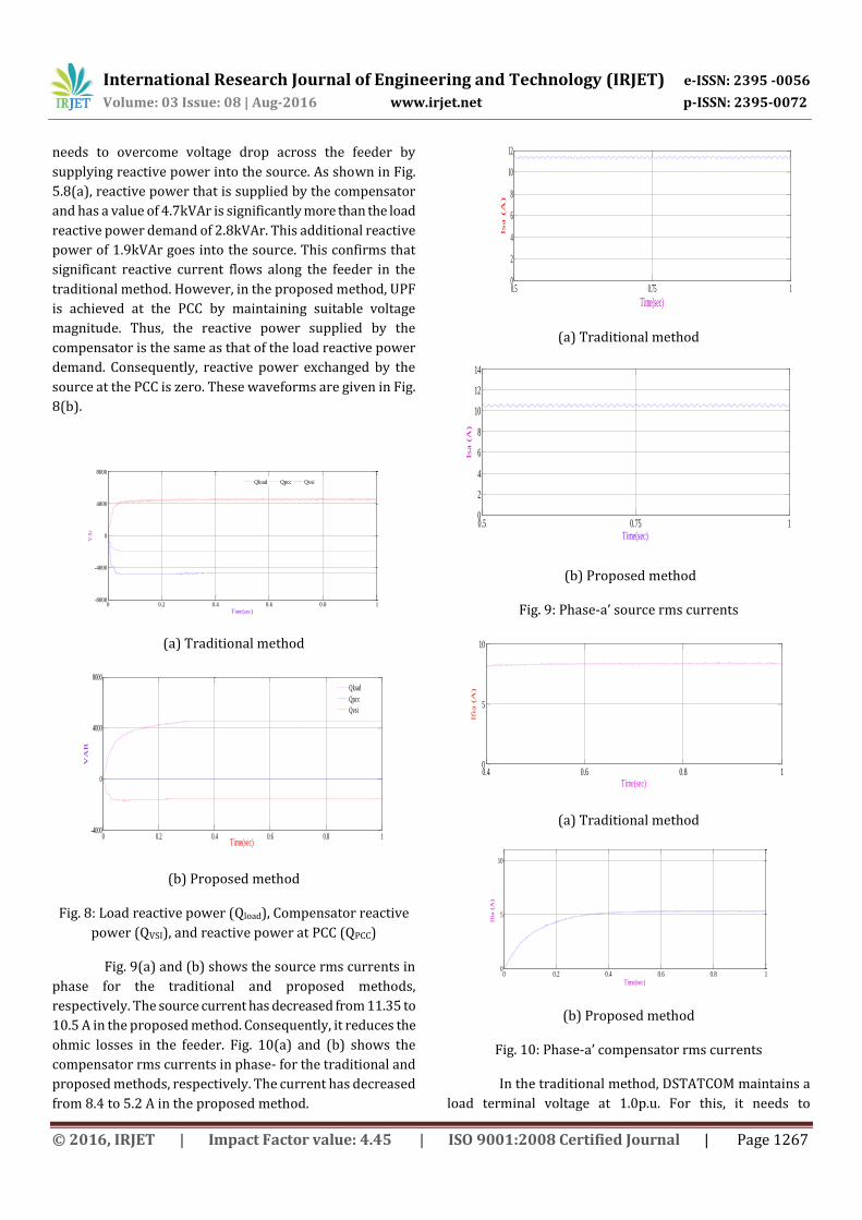
Fig. 9(a) and (b) shows the source rms currents in
phase for the traditional and proposed methods,
respectively. The source current has decreased from 11.35 to
10.5 A in the proposed method. Consequently, it reduces the
ohmic losses in the feeder. Fig. 10(a) and (b) shows the
compensator rms currents in phase- for the traditional and
proposed methods, respectively. The current has decreased
from 8.4 to 5.2 A in the proposed method.
0.5 0.75 10
2
4
6
8
10
12
Time(sec)
Isa (A
)
(a) Traditional method
0.5 0.75 10
2
4
6
8
10
12
14
Time(sec)
Isa (A
)
(b) Proposed method
Fig. 9: Phase-a’ source rms currents
0.4 0.6 0.8 10
5
10
Time(sec)
Ifia (A
)
(a) Traditional method
0 0.2 0.4 0.6 0.8 10
5
10
Time(sec)
Ifia
(A
)
(b) Proposed method
Fig. 10: Phase-a’ compensator rms currents
In the traditional method, DSTATCOM maintains a
load terminal voltage at 1.0p.u. For this, it needs to
Page 6
International Research Journal of Engineering and Technology (IRJET) e-ISSN: 2395 -0056
Volume: 03 Issue: 08 | Aug-2016 www.irjet.net p-ISSN: 2395-0072
© 2016, IRJET | Impact Factor value: 4.45 | ISO 9001:2008 Certified Journal | Page 1268
compensate for the entire feeder drop. Hence, at the steady
state, the compensator supplies reactive power to the source
to overcome this drop. However, in the proposed scheme,
the compensator does not compensate for the feeder drop in
the steady-state condition. Hence, a lesser rating of VSI is
utilized in the steady state. This savings in rating is utilized
to mitigate deep sag, and DSTATCOM capacity to mitigate
deep sag increases.
Operation during Sag
To create sag, source voltage is lowered by 20%
from its nominal value at 0.6 s as shown in Fig. 11(a). Sag is
removed at 1.0 s as shown in Fig. 11(b). Since voltage
regulation capability does not depend upon reference
voltage, it is not shown separately for the traditional method.
Fig. 11(c) and (d) shows terminal voltages regulated at their
reference value.
The controller provides a fast voltage regulation at
the load terminal. Fig. 11(e) shows the total dc bus
voltage. During the transient period, capacitors supply real
power to maintain load power which results in discharging
of capacitors.
If the rating of VSI is limited to mitigate 20% sag,
then this savings in rating can be used to mitigate additional
sag.
0.58 0.59 0.6 0.61 0.62 0.63 0.64
-400
-200
0
200
400
Time(sec)
Vsabc(V
)
Vsa Vsb Vsc
(a) Source voltages during normal to sag
0.98 0.99 1 1.01 1.02 1.03 1.04-400
-200
0
200
400
Time(sec)
Vsab
c(V
)
Vsa Vsb Vsc
(b) Source voltages during sag to normal
0.58 0.59 0.6 0.61 0.62 0.63 0.64-400
-300
-200
-100
0
100
200
300
400
Time(sec)
Vtabc(V)
Vta Vtb Vtc
(c) Terminal voltages during normal to sag
0.98 0.99 1 1.01 1.02 1.03 1.04-400
-200
0
200
400
Time (sec)
Vta
bc (
V)
Vta Vtb Vtc
(d) Terminal voltages during sag to normal
0 0.5 1 1.50
400
800
1200
1600
Time(sec)
Vdc1+
Vdc2 (V
)
(e) Voltage at the dc bus
Fig. 11: Various waveforms during sag operation
To show the capability of DSTATCOM to mitigate
deep sag for a longer time, the source voltage is decreased to
60% of the nominal value for t =1 to 3s duration as shown in
Fig. 12(a). The terminal voltages, maintained at the reference
value, are shown in Fig. 12(b). The voltage across the dc bus
is shown in Fig. 12(c). During transients, this voltage
deviates from its reference voltage. However, it is brought
back to the reference value once steady state is reached.
These waveforms confirm that the DSTATCOM has the
Page 7
International Research Journal of Engineering and Technology (IRJET) e-ISSN: 2395 -0056
Volume: 03 Issue: 08 | Aug-2016 www.irjet.net p-ISSN: 2395-0072
© 2016, IRJET | Impact Factor value: 4.45 | ISO 9001:2008 Certified Journal | Page 1269
capability to mitigate deep sag independent of duration.
However, it requires a high current rating of the VSI.
0 1 2 3 4 5-400
-200
0
200
400
Time(sec)
Vsab
c(V
)
Vsa Vsb Vsc
(a) Source voltages
0 1 2 3 4 5-400
-200
0
200
400
Time(sec)
Vta
bc(V
)
Vta Vtb Vtc
(b) Terminal voltages
0 0.5 1 1.5 2 2.5 3 3.5 4 4.5 50
0.5
1
1.31.5
2
Time(sec)
Vdc1+
Vdc2 (kV
)
(c) Voltage at the dc bus
Fig. 12: Voltage waveforms during sag operation in the
proposed method.
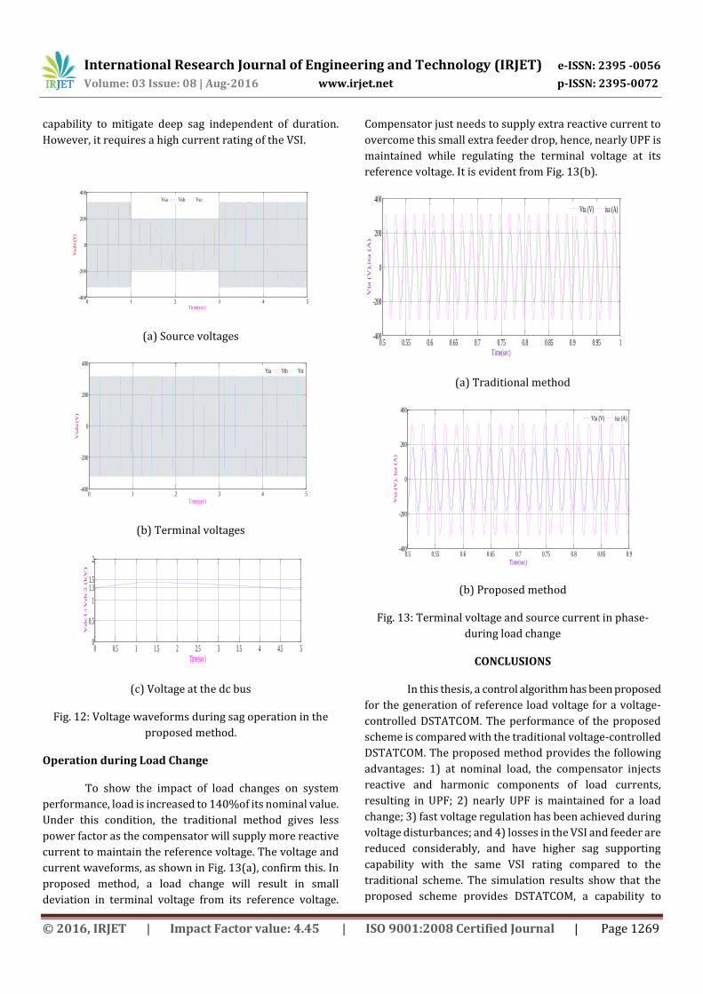
Operation during Load Change
To show the impact of load changes on system
performance, load is increased to 140%of its nominal value.
Under this condition, the traditional method gives less
power factor as the compensator will supply more reactive
current to maintain the reference voltage. The voltage and
current waveforms, as shown in Fig. 13(a), confirm this. In
proposed method, a load change will result in small
deviation in terminal voltage from its reference voltage.
Compensator just needs to supply extra reactive current to
overcome this small extra feeder drop, hence, nearly UPF is
maintained while regulating the terminal voltage at its
reference voltage. It is evident from Fig. 13(b).
0.5 0.55 0.6 0.65 0.7 0.75 0.8 0.85 0.9 0.95 1-400
-200
0
200
400
Time(sec)
Vta (V
),isa (A
)
Vta (V) isa (A)
(a) Traditional method
0.5 0.55 0.6 0.65 0.7 0.75 0.8 0.85 0.9-400
-200
0
200
400
Time(sec)
Vta (V
), isa (A
)
Vta (V) isa (A)
(b) Proposed method
Fig. 13: Terminal voltage and source current in phase-
during load change
CONCLUSIONS
In this thesis, a control algorithm has been proposed
for the generation of reference load voltage for a voltage-
controlled DSTATCOM. The performance of the proposed
scheme is compared with the traditional voltage-controlled
DSTATCOM. The proposed method provides the following
advantages: 1) at nominal load, the compensator injects
reactive and harmonic components of load currents,
resulting in UPF; 2) nearly UPF is maintained for a load
change; 3) fast voltage regulation has been achieved during
voltage disturbances; and 4) losses in the VSI and feeder are
reduced considerably, and have higher sag supporting
capability with the same VSI rating compared to the
traditional scheme. The simulation results show that the
proposed scheme provides DSTATCOM, a capability to
Page 8
International Research Journal of Engineering and Technology (IRJET) e-ISSN: 2395 -0056
Volume: 03 Issue: 08 | Aug-2016 www.irjet.net p-ISSN: 2395-0072
© 2016, IRJET | Impact Factor value: 4.45 | ISO 9001:2008 Certified Journal | Page 1270
improve several PQ problems (related to voltage and
current).
FUTURESCOPE
The proposed method will also validate through any
simulation software packages and it will possible to
implement experimentally.
REFERENCES
[1]. M. Bollen, Understanding Power Quality Problems.
Piscataway, NJ, USA: IEEE, 2000, ch. 1, pp. 1–35.
[2]. Fujita and H. Akagi, “Voltage-regulation
performance of a shunt active filter intended for
installation on a power distribution system,” IEEE
Trans. Power Electron., vol. 22, no. 3, pp. 1046–1053,
May 2007.
[3]. A. Ghosh and G. Ledwich, “Load compensating
DSTATCOM in weak ac systems,” IEEE Trans. Power
Del., vol. 18, no. 4, pp. 1302–1309, Oct. 2003.
[4]. A. Elnady and M. Salama, “Unified approach for
mitigating voltage sag and voltage flicker using the
DSTATCOM,” IEEE Trans. Power Del., vol. 20, no. 2,
pt. 1, pp. 992–1000, Apr. 2005.
[5]. S. Rahmani, A. Hamadi, and K. Al-Haddad, “A
Lyapunov-functionbased control for a three-phase
shunt hybrid active filter,” IEEE Trans. Ind. Electron.,
vol. 59, no. 3, pp. 1418–1429, Mar. 2012.
[6]. M. K. Mishra and K. Karthikeyan, “A fast-acting dc-
link voltage controller for three-phase DSTATCOM
to compensate ac and dc loads,” IEEE Trans. Power
Del., vol. 24, no. 4, pp. 2291–2299, Oct. 2009.
[7]. M. K. Mishra, A. Ghosh, A. Joshi, and H. M.
Suryawanshi, “A novel method of load
compensation under unbalanced and distorted
voltages,” IEEE Trans. Power Del., vol. 22, no. 1, pp.
288–295, Jan. 2007.