International Journal of Science and Research (IJSR) ISSN (Online): 2319-7064 Impact Factor (2012): 3.358 Volume 3 Issue 7, July 2014 www.ijsr.net Licensed Under Creative Commons Attribution CC BY Power Reduction Approach in Combinational Circuit (Half and Full Subtractor) Navendra Rawat, Rakesh Jain Corresponding Author, Department of Electronics and Communication Engineering, Suresh Gyan Vihar University, Jagatpura Mahal, Jaipur, India Assistant Professor, Department of Electronics and Communication Engineering, Suresh Gyan Vihar University, Jagatpura Mahal, Jaipur, India Abstract: The increasing market of mobile devices and battery operated portable electronic systems has led to the demands for chips that consume smallest possible amount of power and equally having high chip density and high throughput during recent years. The purpose of this design is to develop a subtractor circuit that meets the requirement for minimum power dissipation as well as not growing too much in size but if possible than minimize the size too. These goals are achieved using and comparing different techniques including alternate design for AND function. The other two techniques are Drain Gating and LECTOR. Keywords: Standby power dissipation, Subtractor, Drain gating, Lector. 1. Introduction Power dissipation in digital circuits is a cause of concern as it reduces the chip life and efficiency of the circuits as a result of overheating of circuit. Thus, there is a need to reduce the power dissipation as much as possible. In today’s world of technology use of portable devices such as laptops, cell phones and computer has been increased. Power and area consumption has become major concern in schematic design of these portable devices before their actual implementation in the layout. Batteries used in these portable devices have ability to supply limited power. So the no of transistors used in these portable devices must be less as possible to consume less power and area. Also the cost and complexity of any VLSI circuit also depends on the large power dissipation in that circuit. Increased rate of transistors on a single chip can cause increase in both static and dynamic power consumption. Subtractor is one of the most critical components used in the processor of these portable devices. So the area and power efficient design of 1-bit Subtractor is necessary for design of small size portable devices. There is various possible logic styles that can give better performance as compared to the basic CMOS logic style. The performance estimation of 1- Bit full Subtractor is based on area and power consumption, power delay and Power –Delay Product. Area, speed and power consumption are the main issues in VLSI design which often conflict with each other and the design methodology and act as constrain on the design of VLSI circuits. These performance criteria’s should be individually investigated, analyzed for the various designs of the 1-Bit Subtractor by using different logic styles. In this paper a study has been done on the effects of various previously implemented power reduction techniques on a Subtractor and also a new and improved technique has been introduced for the same purpose. There are presently 3 power reduction techniques which are: Power Gating, Drain Gating and Transistor Gating. In all of these techniques the objective is to reduce the power dissipated by the circuit when it is in standby mode. The leakage or static power dissipation, which is the power dissipated by the circuit when it is in standby mode is given by: DD V leak I leak P (1) Where, I leak is the leakage current which flows when the circuit is OFF and V DD is the supply voltage. In all of the above mentioned techniques, the aim is to reduce this leakage current I leak by adding extra (sleep) transistors in the circuit in the path between power supply (VDD) and ground. These extra transistors are inserted in such a way that the path between power supply and ground is cut-off, so that no leakage current occurs, thereby eliminating standby power dissipation. In addition to these existing power reduction techniques, a new technique (LECTOR) has been introduced to reduce standby/leakage power. Subsequently, standby power is computed for a conventional CMOS Subtractor, implemented using one of the existing techniques called Drain Gating and also for NAND gate implemented using the proposed technique at 5 volt voltage at .25 micro meter technology. This data is compiled in a tabular form. The table reflects that in all the techniques as well as conventional CMOS Subtractor, standby power dissipation is directly proportional to no. of transistor used in the circuit i.e. with an increase in no. of transistors used in circuit, standby power dissipation increases. Moreover, the table depicts significantly lower power dissipation (standby) in the proposed design as compared to the power dissipation in the conventional CMOS Subtractor as well as other existing power reduction techniques. Power dissipation is an important consideration in the design of CMOS VLSI circuits. High power consumption leads to reduction in the battery life in the case of battery-powered applications and affects reliability, packaging and cooling costs. The main sources for power dissipation are: 1. Capacitive power dissipation 2. Short circuit currents and 3. Leakage currents Paper ID: 020141188 1104
Transcript
International Journal of Science and Research (IJSR) ISSN (Online): 2319-7064
Impact Factor (2012): 3.358
Volume 3 Issue 7, July 2014 www.ijsr.net
Licensed Under Creative Commons Attribution CC BY
Power Reduction Approach in Combinational Circuit (Half and Full Subtractor)
Navendra Rawat, Rakesh Jain
Corresponding Author, Department of Electronics and Communication Engineering, Suresh Gyan Vihar University,
Jagatpura Mahal, Jaipur, India
Assistant Professor, Department of Electronics and Communication Engineering, Suresh Gyan Vihar University, Jagatpura Mahal, Jaipur, India
Abstract: The increasing market of mobile devices and battery operated portable electronic systems has led to the demands for chips that consume smallest possible amount of power and equally having high chip density and high throughput during recent years. The purpose of this design is to develop a subtractor circuit that meets the requirement for minimum power dissipation as well as not growing too much in size but if possible than minimize the size too. These goals are achieved using and comparing different techniques including alternate design for AND function. The other two techniques are Drain Gating and LECTOR. Keywords: Standby power dissipation, Subtractor, Drain gating, Lector.
1. Introduction Power dissipation in digital circuits is a cause of concern as it reduces the chip life and efficiency of the circuits as a result of overheating of circuit. Thus, there is a need to reduce the power dissipation as much as possible. In today’s world of technology use of portable devices such as laptops, cell phones and computer has been increased. Power and area consumption has become major concern in schematic design of these portable devices before their actual implementation in the layout. Batteries used in these portable devices have ability to supply limited power. So the no of transistors used in these portable devices must be less as possible to consume less power and area. Also the cost and complexity of any VLSI circuit also depends on the large power dissipation in that circuit. Increased rate of transistors on a single chip can cause increase in both static and dynamic power consumption.
Subtractor is one of the most critical components used in the processor of these portable devices. So the area and power efficient design of 1-bit Subtractor is necessary for design of small size portable devices. There is various possible logic styles that can give better performance as compared to the basic CMOS logic style. The performance estimation of 1-Bit full Subtractor is based on area and power consumption, power delay and Power –Delay Product. Area, speed and power consumption are the main issues in VLSI design which often conflict with each other and the design methodology and act as constrain on the design of VLSI circuits. These performance criteria’s should be individually investigated, analyzed for the various designs of the 1-Bit Subtractor by using different logic styles. In this paper a study has been done on the effects of various previously implemented power reduction techniques on a Subtractor and also a new and improved technique has been introduced for the same purpose. There are presently 3 power reduction techniques which are: Power Gating, Drain Gating and Transistor Gating. In all of these techniques the objective is to reduce the power dissipated by the circuit when it is in standby mode. The leakage or static power dissipation,
which is the power dissipated by the circuit when it is in standby mode is given by:
DDV
leakI
leakP (1)
Where, Ileak is the leakage current which flows when the circuit is OFF and VDD is the supply voltage. In all of the above mentioned techniques, the aim is to reduce this leakage current Ileak by adding extra (sleep) transistors in the circuit in the path between power supply (VDD) and ground. These extra transistors are inserted in such a way that the path between power supply and ground is cut-off, so that no leakage current occurs, thereby eliminating standby power dissipation. In addition to these existing power reduction techniques, a new technique (LECTOR) has been introduced to reduce standby/leakage power. Subsequently, standby power is computed for a conventional CMOS Subtractor, implemented using one of the existing techniques called Drain Gating and also for NAND gate implemented using the proposed technique at 5 volt voltage at .25 micro meter technology. This data is compiled in a tabular form. The table reflects that in all the techniques as well as conventional CMOS Subtractor, standby power dissipation is directly proportional to no. of transistor used in the circuit i.e. with an increase in no. of transistors used in circuit, standby power dissipation increases. Moreover, the table depicts significantly lower power dissipation (standby) in the proposed design as compared to the power dissipation in the conventional CMOS Subtractor as well as other existing power reduction techniques. Power dissipation is an important consideration in the design of CMOS VLSI circuits. High power consumption leads to reduction in the battery life in the case of battery-powered applications and affects reliability, packaging and cooling costs. The main sources for power dissipation are:
1. Capacitive power dissipation 2. Short circuit currents and 3. Leakage currents
Paper ID: 020141188 1104
International Journal of Science and Research (IJSR) ISSN (Online): 2319-7064
Impact Factor (2012): 3.358
Volume 3 Issue 7, July 2014 www.ijsr.net
Licensed Under Creative Commons Attribution CC BY
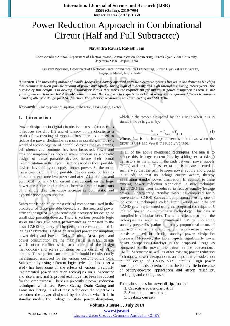
With technology processes advancing towards deep submicron and nano regimes, the scaling down of the threshold voltage levels in turn causes an exponential increase in subthreshold leakage currents leading to increase in leakage power. With the advance of each generation of the fabrication process, there is a five-fold increase in leakage power dissipation. Leakage currents flow when the circuit is idle and hence is wasted power. Efficient leakage power reduction techniques have become critical for the deep submicron and nanometer circuits. A new technique called LECTOR (based on LEakage Control Transistors) for leakage reduction in CMOS circuits is used. 2. Literature Survey 2.1 Half Subtractor The half-subtractor is a combinational circuit which is used to perform subtraction of two bits. It has two inputs, X (minuend) and Y (subtrahend) and two outputs D (difference) and B (borrow).
Table 1: Truth Table for Half Subtractor X Y D B 0 0 0 0 0 1 1 1 1 0 1 0 1 1 0 0
Figure 1: Logic Diagram for Half Subtractor
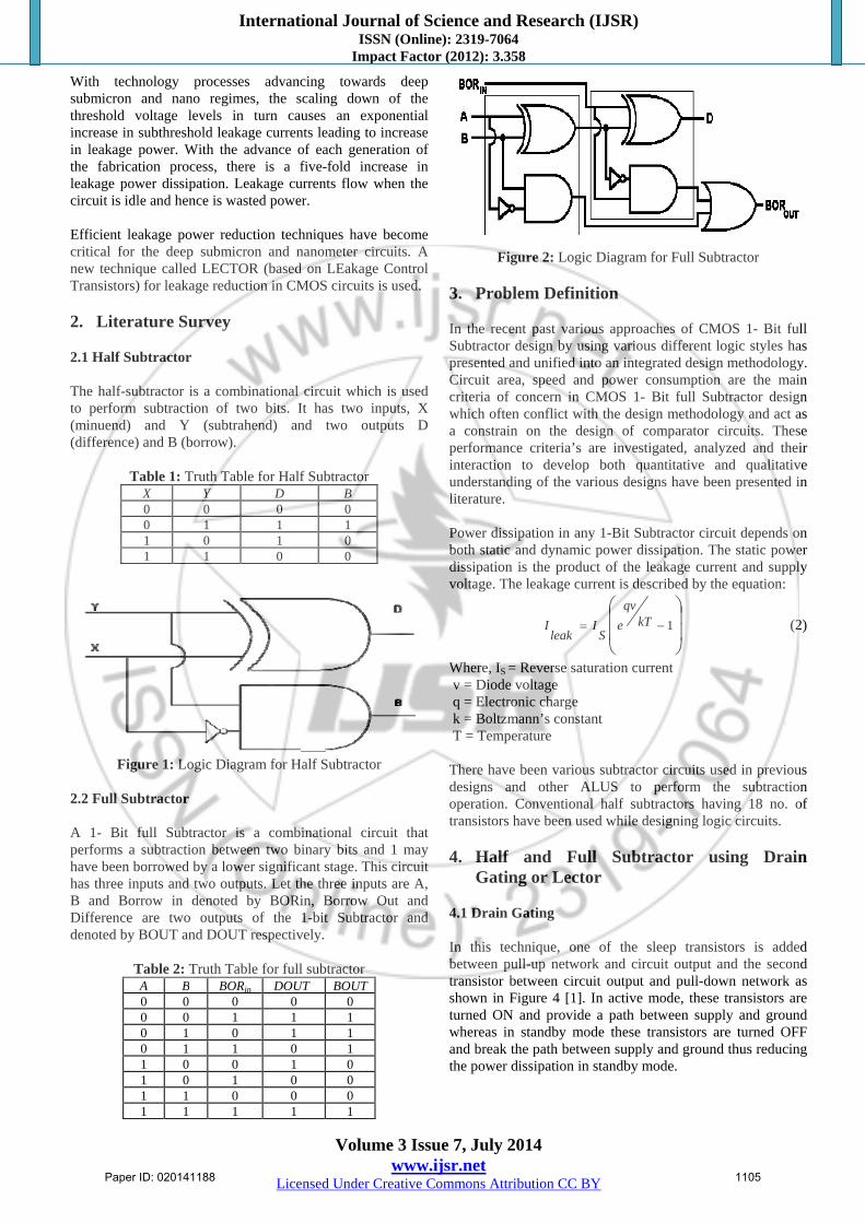
2.2 Full Subtractor A 1- Bit full Subtractor is a combinational circuit that performs a subtraction between two binary bits and 1 may have been borrowed by a lower significant stage. This circuit has three inputs and two outputs. Let the three inputs are A, B and Borrow in denoted by BORin, Borrow Out and Difference are two outputs of the 1-bit Subtractor and denoted by BOUT and DOUT respectively.
In the recent past various approaches of CMOS 1- Bit full Subtractor design by using various different logic styles has presented and unified into an integrated design methodology. Circuit area, speed and power consumption are the main criteria of concern in CMOS 1- Bit full Subtractor design which often conflict with the design methodology and act as a constrain on the design of comparator circuits. These performance criteria’s are investigated, analyzed and their interaction to develop both quantitative and qualitative understanding of the various designs have been presented in literature. Power dissipation in any 1-Bit Subtractor circuit depends on both static and dynamic power dissipation. The static power dissipation is the product of the leakage current and supply voltage. The leakage current is described by the equation:
1kT
qv
eS
Ileak
I (2)
Where, IS = Reverse saturation current v = Diode voltage q = Electronic charge k = Boltzmann’s constant T = Temperature There have been various subtractor circuits used in previous designs and other ALUS to perform the subtraction operation. Conventional half subtractors having 18 no. of transistors have been used while designing logic circuits. 4. Half and Full Subtractor using Drain
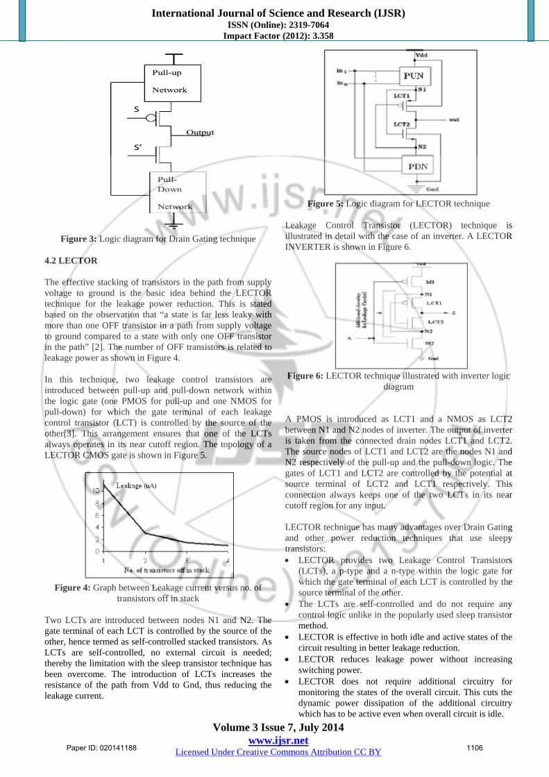
Gating or Lector 4.1 Drain Gating In this technique, one of the sleep transistors is added between pull-up network and circuit output and the second transistor between circuit output and pull-down network as shown in Figure 4 [1]. In active mode, these transistors are turned ON and provide a path between supply and ground whereas in standby mode these transistors are turned OFF and break the path between supply and ground thus reducing the power dissipation in standby mode.
Paper ID: 020141188 1105
International Journal of Science and Research (IJSR) ISSN (Online): 2319-7064
Impact Factor (2012): 3.358
Volume 3 Issue 7, July 2014 www.ijsr.net
Licensed Under Creative Commons Attribution CC BY
Figure 3: Logic diagram for Drain Gating technique
4.2 LECTOR The effective stacking of transistors in the path from supply voltage to ground is the basic idea behind the LECTOR technique for the leakage power reduction. This is stated based on the observation that “a state is far less leaky with more than one OFF transistor in a path from supply voltage to ground compared to a state with only one OFF transistor in the path” [2]. The number of OFF transistors is related to leakage power as shown in Figure 4. In this technique, two leakage control transistors are introduced between pull-up and pull-down network within the logic gate (one PMOS for pull-up and one NMOS for pull-down) for which the gate terminal of each leakage control transistor (LCT) is controlled by the source of the other[3]. This arrangement ensures that one of the LCTs always operates in its near cutoff region. The topology of a LECTOR CMOS gate is shown in Figure 5.
Figure 4: Graph between Leakage current versus no. of
transistors off in stack Two LCTs are introduced between nodes N1 and N2. The gate terminal of each LCT is controlled by the source of the other, hence termed as self-controlled stacked transistors. As LCTs are self-controlled, no external circuit is needed; thereby the limitation with the sleep transistor technique has been overcome. The introduction of LCTs increases the resistance of the path from Vdd to Gnd, thus reducing the leakage current.
Figure 5: Logic diagram for LECTOR technique
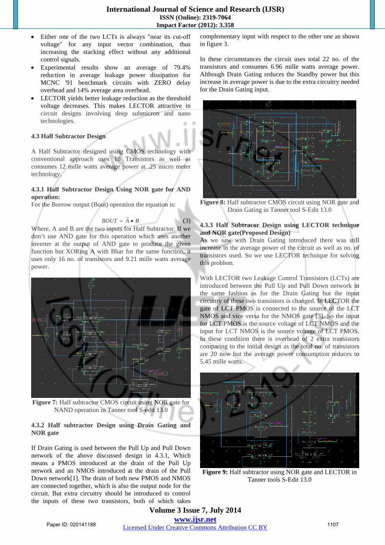
Leakage Control Transistor (LECTOR) technique is illustrated in detail with the case of an inverter. A LECTOR INVERTER is shown in Figure 6.
Figure 6: LECTOR technique illustrated with inverter logic
diagram A PMOS is introduced as LCT1 and a NMOS as LCT2 between N1 and N2 nodes of inverter. The output of inverter is taken from the connected drain nodes LCT1 and LCT2. The source nodes of LCT1 and LCT2 are the nodes N1 and N2 respectively of the pull-up and the pull-down logic. The gates of LCT1 and LCT2 are controlled by the potential at source terminal of LCT2 and LCT1 respectively. This connection always keeps one of the two LCTs in its near cutoff region for any input. LECTOR technique has many advantages over Drain Gating and other power reduction techniques that use sleepy transistors: LECTOR provides two Leakage Control Transistors
(LCTs), a p-type and a n-type within the logic gate for which the gate terminal of each LCT is controlled by the source terminal of the other.
The LCTs are self-controlled and do not require any control logic unlike in the popularly used sleep transistor method.
LECTOR is effective in both idle and active states of the circuit resulting in better leakage reduction.
LECTOR reduces leakage power without increasing switching power.
LECTOR does not require additional circuitry for monitoring the states of the overall circuit. This cuts the dynamic power dissipation of the additional circuitry which has to be active even when overall circuit is idle.
Paper ID: 020141188 1106
International Journal of Science and Research (IJSR) ISSN (Online): 2319-7064
Impact Factor (2012): 3.358
Volume 3 Issue 7, July 2014 www.ijsr.net
Licensed Under Creative Commons Attribution CC BY
Either one of the two LCTs is always "near its cut-off voltage" for any input vector combination, thus increasing the stacking effect without any additional control signals.
Experimental results show an average of 79.4% reduction in average leakage power dissipation for MCNC '91 benchmark circuits with ZERO delay overhead and 14% average area overhead.
LECTOR yields better leakage reduction as the threshold voltage decreases. This makes LECTOR attractive in circuit designs involving deep submicron and nano technologies.
4.3 Half Subtractor Design A Half Subtractor designed using CMOS technology with conventional approach uses 18 Transistors as well as consumes 12 mille watts average power at .25 micro meter technology. 4.3.1 Half Subtractor Design Using NOR gate for AND operation: For the Borrow output (Bout) operation the equation is:
BABOUT (3) Where, A and B are the two inputs for Half Subtractor. If we don’t use AND gate for this operation which uses another inverter at the output of AND gate to produce the given function but XORing A with Bbar for the same function, it uses only 16 no. of transistors and 9.21 mille watts average power.
Figure 7: Half subtractor CMOS circuit using NOR gate for
NAND operation in Tanner tool S-edit 13.0 4.3.2 Half subtractor Design using Drain Gating and NOR gate If Drain Gating is used between the Pull Up and Pull Down network of the above discussed design in 4.3.1, Which means a PMOS introduced at the drain of the Pull Up network and an NMOS introduced at the drain of the Pull Down network[1]. The drain of both new PMOS and NMOS are connected together, which is also the output node for the circuit. But extra circuitry should be introduced to control the inputs of these two transistors, both of which takes
complementary input with respect to the other one as shown in figure 3. In these circumstances the circuit uses total 22 no. of the transistors and consumes 6.96 mille watts average power. Although Drain Gating reduces the Standby power but this increase in average power is due to the extra circuitry needed for the Drain Gating input.
Figure 8: Half subtractor CMOS circuit using NOR gate and
Drain Gating in Tanner tool S-Edit 13.0 4.3.3 Half Subtracor Design using LECTOR technique and NOR gate(Proposed Design) As we saw with Drain Gating introduced there was still increase in the average power of the circuit as well as no. of transistors used. So we use LECTOR technique for solving this problem. With LECTOR two Leakage Control Transistors (LCTs) are introduced between the Pull Up and Pull Down network in the same fashion as for the Drain Gating but the input circuitry of these two transistors is changed. In LECTOR the gate of LCT PMOS is connected to the source of the LCT NMOS and vice versa for the NMOS gate [3]. So the input for LCT PMOS is the source voltage of LCT NMOS and the input for LCT NMOS is the source voltage of LCT PMOS. In these condition there is overhead of 2 extra transistors comparing to the initial design as the total no. of transistors are 20 now but the average power consumption reduces to 5.45 mille watts.
Figure 9: Half subtractor using NOR gate and LECTOR in
Tanner tools S-Edit 13.0
Paper ID: 020141188 1107
International Journal of Science and Research (IJSR) ISSN (Online): 2319-7064
Impact Factor (2012): 3.358
Volume 3 Issue 7, July 2014 www.ijsr.net
Licensed Under Creative Commons Attribution CC BY
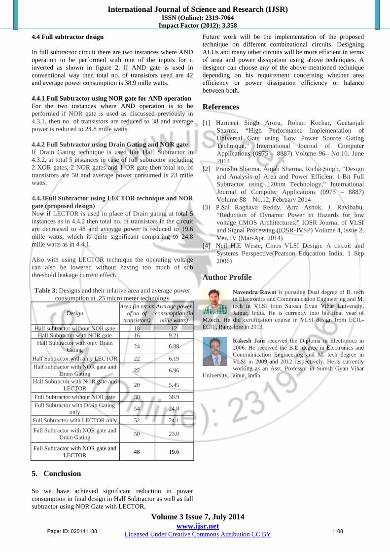
4.4 Full subtractor design In full subtractor circuit there are two instances where AND operation to be performed with one of the inputs for it inverted as shown in figure 2. If AND gate is used in conventional way then total no. of transistors used are 42 and average power consumption is 38.9 mille watts. 4.4.1 Full Subtractor using NOR gate for AND operation For the two instances where AND operation is to be performed if NOR gate is used as discussed previously in 4.3.1, then no. of transistors are reduced to 38 and average power is reduced to 24.8 mille watts. 4.4.2 Full Subtractor using Drain Gating and NOR gate If Drain Gating technique is used like Half Subtractor in 4.3.2, at total 5 instances in case of full subtractor including 2 XOR gates, 2 NOR gates and 1 OR gate then total no. of transistors are 50 and average power consumed is 23 mille watts. 4.4.3Full Subtractor using LECTOR technique and NOR gate (proposed design) Now if LECTOR is used in place of Drain gating at total 5 instances as in 4.4.2 then total no. of transistors in the circuit are decreased to 48 and average power is reduced to 19.6 mille watts, which is quite significant comparing to 24.8 mille watts as in 4.4.1. Also with using LECTOR technique the operating voltage can also be lowered without having too much of sub threshold leakage current effect. Table 3: Designs and their relative area and average power
consumption at .25 micro meter technology
Design Area (in terms
of no. of transistors)
Average power consumption (in
mille watts) Half subtractor without NOR gate 18 12
Half Subtractor with NOR gate 16 9.21Half Subtractor with only Drain
Gating 24 6.88
Half Subtractor with only LECTOR 22 6.19
Half subtractor with NOR gate and Drain Gating
22 6.96
Half Subtractor with NOR gate and LECTOR
20 5.45
Full Subtractor without NOR gate 38 38.9
Full Subtractor with Drain Gating only
54 24.8
Full Subtractor with LECTOR only 52 24.1
Full Subtractor with NOR gate and Drain Gating
50 23.0
Full Subtractor with NOR gate and LECTOR
48 19.6
5. Conclusion
So we have achieved significant reduction in power consumption in final design in Half Subtractor as well as full subtractor using NOR Gate with LECTOR.
Future work will be the implementation of the proposed technique on different combinational circuits. Designing ALUs and many other circuits will be more efficient in terms of area and power dissipation using above techniques. A designer can choose any of the above mentioned technique depending on his requirement concerning whether area efficiency or power dissipation efficiency or balance between both. References [1] Harmeet Singh Arora, Rohan Kochar, Geetanjali
Sharma, “High Performance Implementation of Universal Gate using Low Power Source Gating Technique,” International Journal of Computer Applications (0975 – 8887) Volume 96– No.10, June 2014
[2] Pranshu Sharma, Anjali Sharma, Richa Singh, “Design and Analysis of Area and Power Efficient 1-Bit Full Subtractor using 120nm Technology,” International Journal of Computer Applications (0975 – 8887) Volume 88 – No.12, February 2014
[3] P.Sai Raghava Reddy, Arra Ashok, J. Ravibabu, “Reduction of Dynamic Power in Hazards for low voltage CMOS Architectures,” IOSR Journal of VLSI and Signal Processing (IOSR-JVSP) Volume 4, Issue 2, Ver. IV (Mar-Apr. 2014)
[4] Neil H.E Weste, Cmos VLSI Design: A circuit and Systems Perspective(Pearson Education India, 1 Sep 2006)
Author Profile
Navendra Rawat is pursuing Dual degree of B. tech in Electronics and Communication Engineering and M. tech in VLSI from Suresh Gyan Vihar University, Jaipur, India. He is currently into his final year of
M.tech. He did certification course in VLSI design from ECIL-ECIT, Bangalore in 2013.
Rakesh Jain received the Diploma in Electronics in 2006. He received the B.E. degree in Electronics and Communication Engineering and M. tech degree in VLSI in 2009 and 2012 respectively. He is currently working as an Asst. Professor in Suresh Gyan Vihar