Engineering Report Please read the Important Notice and Warnings at the end of this document <Revision 1.0> www.infineon.com 2016-12-13 ER_201612_PL16_04 Power Tools ME/MF DirectFET™ Kit About this document This application note presents the description of the Infineon’s demo board for cordless power tools. The current design considers the electrical driving capabilities for brushless DC (BLDC) machines with three hall sensors used for rotor position detection and speed measurement. This board utilises the ME/MF DirectFET TM power devices (IRF7480/IRF7483) and the firmware is developed using the XMC TM 1300 family (www.infineon.com/XMC). The source code, available in the package, is completely implemented using the Infineon Eclipse-based IDE, DAVE TM (Development Platform for XMC TM Microcontroller) (www.infineon.com/DAVE). The control method implements a scalar speed control algorithm based on the brushless DC motor (BLDC) using pulse-width modulation (PWM) and three hall sensors. With this kit, users can evaluate the properties of the low R DS(ON) low voltage Infineon DirectFET TM using the control capabilities of the XMC TM 1300 by means of the implemented control algorithm BLDC_SCALAR_HALL_XMC13 with customised features for power tools application. Scope and purpose This document intends to describe the functionalities of the Power Tools DirectFET TM ME/MF Kit for motor control applications, more specifically for cordless BLDC drives in battery powered power tools when three hall sensors are available for speed and rotor position sensing. Together with the Infineon DirectFET TM low R DS(ON) low voltage MOSFETs, such solution can help reduce system cost and time to market while at the same time significantly increase the power density, system performance and peak power pulse capabilities. Intended audience This document addresses the market for cordless power tool manufactures who intend to provide to a high performance system solution as well as reduce the system costs. Table of Contents About this document ............................................................................................................................1 Table of Contents .................................................................................................................................1 1 Power Tools ME/MF DirectFET TM Kit ...............................................................................3 1.1 Overview ............................................................................................................................................ 3 1.1.1 Key Features.................................................................................................................................. 5 1.2 System Block Diagram .......................................................................................................................6 1.3 Hardware Description ......................................................................................................................... 7 1.3.1 Power Supplies ..............................................................................................................................8 1.3.2 Overcurrent Protection .................................................................................................................9 1.3.3 Over-Temperature Protection ..................................................................................................... 11 1.3.4 Gate Drivers ................................................................................................................................ 11 1.3.5 Heatsink and Gap Pad ................................................................................................................. 12 1.4 System Power Up ............................................................................................................................. 16 1.5 Getting Started with the Infineon Power Tools DirectFET TM Kit ....................................................... 17 1.5.1 Getting Started with DAVE TM (Version 4) .................................................................................... 17 1.5.2 Parameters Selection and Settings .............................................................................................. 19 1.5.3 Compilation and Debug Session .................................................................................................. 23 1.5.4 Acquisition of Hall and Multichannel PWM Patterns .................................................................... 25 1.6 System Operation ............................................................................................................................ 27 1.6.1 Modulation Signals and Main Waveforms.................................................................................... 27
Transcript
Engineering Report Please read the Important Notice and Warnings at the end of this document <Revision 1.0>
www.infineon.com 2016-12-13
ER_201612_PL16_04
Power Tools
ME/MF DirectFET™ Kit
About this document
This application note presents the description of the Infineon’s demo board for cordless power tools. The current design considers the electrical driving capabilities for brushless DC (BLDC) machines with three hall sensors used for rotor position detection and speed measurement. This board utilises the ME/MF DirectFET
TM power devices
(IRF7480/IRF7483) and the firmware is developed using the XMCTM
1300 family (www.infineon.com/XMC). The source code, available in the package, is completely implemented using the Infineon Eclipse-based IDE, DAVE
TM (Development Platform for XMC
TM Microcontroller) (www.infineon.com/DAVE). The control method
implements a scalar speed control algorithm based on the brushless DC motor (BLDC) using pulse-width modulation (PWM) and three hall sensors. With this kit, users can evaluate the properties of the low RDS(ON) low voltage Infineon DirectFET
TM using the control
capabilities of the XMCTM
1300 by means of the implemented control algorithm BLDC_SCALAR_HALL_XMC13 with customised features for power tools application.
Scope and purpose
This document intends to describe the functionalities of the Power Tools DirectFETTM
ME/MF Kit for motor control applications, more specifically for cordless BLDC drives in battery powered power tools when three hall sensors are available for speed and rotor position sensing. Together with the Infineon DirectFET
TM low RDS(ON) low voltage
MOSFETs, such solution can help reduce system cost and time to market while at the same time significantly increase the power density, system performance and peak power pulse capabilities.
Intended audience
This document addresses the market for cordless power tool manufactures who intend to provide to a high performance system solution as well as reduce the system costs.
Table of Contents
About this document ............................................................................................................................1
Table of Contents .................................................................................................................................1
1 Power Tools ME/MF DirectFETTM Kit ...............................................................................3 1.1 Overview ............................................................................................................................................ 3 1.1.1 Key Features .................................................................................................................................. 5 1.2 System Block Diagram .......................................................................................................................6 1.3 Hardware Description ......................................................................................................................... 7 1.3.1 Power Supplies .............................................................................................................................. 8 1.3.2 Overcurrent Protection .................................................................................................................9 1.3.3 Over-Temperature Protection ..................................................................................................... 11 1.3.4 Gate Drivers ................................................................................................................................ 11 1.3.5 Heatsink and Gap Pad ................................................................................................................. 12 1.4 System Power Up ............................................................................................................................. 16 1.5 Getting Started with the Infineon Power Tools DirectFETTM Kit ....................................................... 17 1.5.1 Getting Started with DAVETM (Version 4) .................................................................................... 17 1.5.2 Parameters Selection and Settings .............................................................................................. 19 1.5.3 Compilation and Debug Session .................................................................................................. 23 1.5.4 Acquisition of Hall and Multichannel PWM Patterns .................................................................... 25 1.6 System Operation ............................................................................................................................ 27 1.6.1 Modulation Signals and Main Waveforms.................................................................................... 27
Engineering Report 2 <Revision 1.0> 2016-12-21
Power Tools ME/MF DirectFET™ kitTitle_continued
ER_201612_PL16_04 1.6.2 Overcurrent Protection ............................................................................................................... 31 1.6.3 Temperature Protection .............................................................................................................. 32 1.7 Operating Principle .......................................................................................................................... 35 1.8 Schematic and PCB layout: ............................................................................................................... 40 1.9 Bill of Materials ................................................................................................................................. 45
2 Hall Learning Procedure ..................................................................................................... 47
Revision History ................................................................................................................................. 50
Engineering Report 3 <Revision 1.0> 2016-12-21
Power Tools ME/MF DirectFET™ kitTitle_continued
ER_201612_PL16_04
1 Power Tools ME/MF 1 DirectFET
TM Kit
1.1 Overview
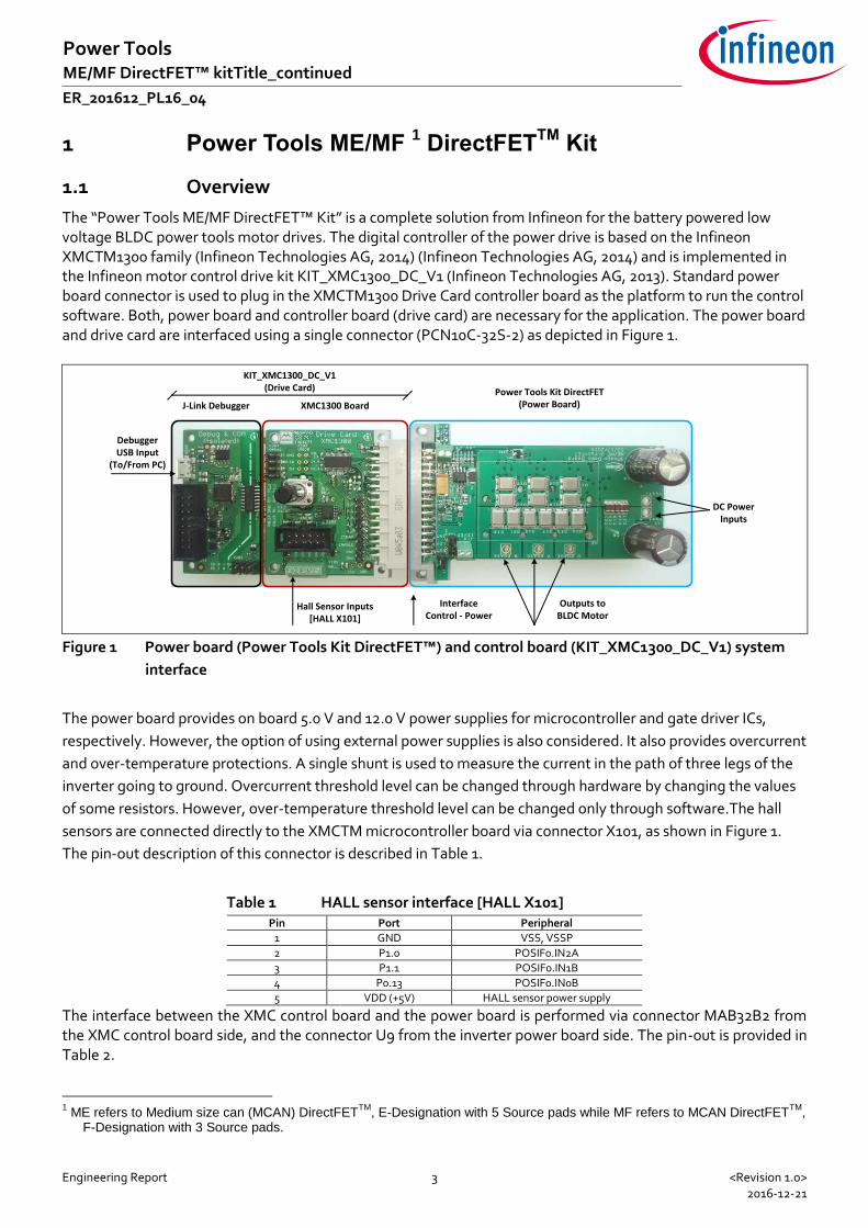
The “Power Tools ME/MF DirectFET™ Kit” is a complete solution from Infineon for the battery powered low voltage BLDC power tools motor drives. The digital controller of the power drive is based on the Infineon XMCTM1300 family (Infineon Technologies AG, 2014) (Infineon Technologies AG, 2014) and is implemented in the Infineon motor control drive kit KIT_XMC1300_DC_V1 (Infineon Technologies AG, 2013). Standard power board connector is used to plug in the XMCTM1300 Drive Card controller board as the platform to run the control software. Both, power board and controller board (drive card) are necessary for the application. The power board and drive card are interfaced using a single connector (PCN10C-32S-2) as depicted in Figure 1.
J-Link Debugger XMC1300 Board
KIT_XMC1300_DC_V1(Drive Card) Power Tools Kit DirectFET
(Power Board)
DebuggerUSB Input
(To/From PC)
Hall Sensor Inputs[HALL X101]
Outputs toBLDC Motor
DC PowerInputs
InterfaceControl - Power
Figure 1 Power board (Power Tools Kit DirectFET™) and control board (KIT_XMC1300_DC_V1) system
interface
The power board provides on board 5.0 V and 12.0 V power supplies for microcontroller and gate driver ICs,
respectively. However, the option of using external power supplies is also considered. It also provides overcurrent
and over-temperature protections. A single shunt is used to measure the current in the path of three legs of the
inverter going to ground. Overcurrent threshold level can be changed through hardware by changing the values
of some resistors. However, over-temperature threshold level can be changed only through software.The hall
sensors are connected directly to the XMCTM microcontroller board via connector X101, as shown in Figure 1.
The pin-out description of this connector is described in Table 1.
Table 1 HALL sensor interface [HALL X101] Pin Port Peripheral
1 GND VSS, VSSP
2 P1.0 POSIF0.IN2A
3 P1.1 POSIF0.IN1B
4 P0.13 POSIF0.IN0B
5 VDD (+5V) HALL sensor power supply
The interface between the XMC control board and the power board is performed via connector MAB32B2 from the XMC control board side, and the connector U9 from the inverter power board side. The pin-out is provided in Table 2.
1 ME refers to Medium size can (MCAN) DirectFET
TM, E-Designation with 5 Source pads while MF refers to MCAN DirectFET
TM,
F-Designation with 3 Source pads.
Engineering Report 4 <Revision 1.0> 2016-12-21
Power Tools ME/MF DirectFET™ kitTitle_continued
ER_201612_PL16_04 Table 2 Power board connector pin-map
1 The numbering of pins in the power board connector is reversed with respect to the numbering in the control board.
Engineering Report 5 <Revision 1.0> 2016-12-21
Power Tools ME/MF DirectFET™ kitTitle_continued
ER_201612_PL16_04 1.1.1 Key Features
The capabilities of the “Power Tools ME/MF DirectFETTM Kit” for cordless battery powered application are as follows:
ME/MF layouts for MCAN DirectFETTM, two MOSFETs in parallel at each leg of the inverter
Standard power board connector to plug in the XMCTM1300
20.0 V nominal input voltage
6.0 V to 40.0 V input voltage range
50.0 APeak and 35 ARMS phase current for continuous operation
200.0 APeak current for 100.0 ms
Latched shut down overcurrent protection through one shunt amplifier
Over-temperature protection with programmable threshold level
5.0 V and 12.0 V on board power supplies for microcontroller and gate drivers, respectively
External power supply options for microcontroller and power MOSFETs gate drivers
Die temperature measurement through openings on bottom side of the PCB
Block commutation modulation method with three hall sensors or back EMF
Scalar BLDC motor speed control with three hall sensors for speed monitoring based on the
BLDC_SCALAR_HALL_XMC13 with improved features for the specific application in cordless power tools
Configurable modulation schemes (high-side modulation with or without synchronous rectification) for
efficiency improvement evaluation
Flexible user configuration capabilities by means of DAVETM (Version 4)
Hall pattern learning by detecting the hall and phase excitation patterns during start-up
Overcurrent protection (adjustable by hardware)
Over-temperature protection (adjustable by software)
Wrong hall pattern protection
Serial interface via USB connection for monitoring of motor variables and parameters using Infineon
μCProbe
Engineering Report 6 <Revision 1.0> 2016-12-21
Power Tools ME/MF DirectFET™ kitTitle_continued
ER_201612_PL16_04 1.2 System Block Diagram
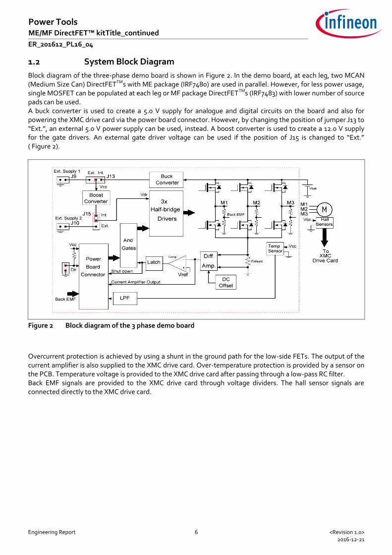
Block diagram of the three-phase demo board is shown in Figure 2. In the demo board, at each leg, two MCAN (Medium Size Can) DirectFETTMs with ME package (IRF7480) are used in parallel. However, for less power usage, single MOSFET can be populated at each leg or MF package DirectFETTMs (IRF7483) with lower number of source pads can be used. A buck converter is used to create a 5.0 V supply for analogue and digital circuits on the board and also for powering the XMC drive card via the power board connector. However, by changing the position of jumper J13 to “Ext.”, an external 5.0 V power supply can be used, instead. A boost converter is used to create a 12.0 V supply for the gate drivers. An external gate driver voltage can be used if the position of J15 is changed to “Ext.” ( Figure 2).
Figure 2 Block diagram of the 3 phase demo board
Overcurrent protection is achieved by using a shunt in the ground path for the low-side FETs. The output of the current amplifier is also supplied to the XMC drive card. Over-temperature protection is provided by a sensor on the PCB. Temperature voltage is provided to the XMC drive card after passing through a low-pass RC filter. Back EMF signals are provided to the XMC drive card through voltage dividers. The hall sensor signals are connected directly to the XMC drive card.
Engineering Report 7 <Revision 1.0> 2016-12-21
Power Tools ME/MF DirectFET™ kitTitle_continued
ER_201612_PL16_04 1.3 Hardware Description
Different circuit sections on the demo board (power board side) are shown in Figure 3 and Figure 4. An aluminium heatsink is attached on top of the DirectFETTMs. Sil-Pad, a thermally conductive insulator is used between the heatsink and DirectFETTMs. Some openings are made on the PCB to facilitate the measurement of the die temperature of DirectFETTMs using an infrared thermal camera.
Outputs to
BLDC Motor
Input
Supply MCAN DirectFETTM
s
External
Supply 2
Po
we
r B
oa
rd
Co
nn
ec
tor
BuckTemperature
SensorExternal
Supply 1
EN-LED
Figure 3 Different hardware sections shown on the demo board (top side)
Latch
Comparator
Differential
Amplifier
AND Gates
Gate Drivers
Curent
Shunt
Buck
Output
Filter
Boost
J13
Die Temperature
Measuring Points
Figure 4 Different hardware sections shown on the demo board (bottom side)
Engineering Report 8 <Revision 1.0> 2016-12-21
Power Tools ME/MF DirectFET™ kitTitle_continued
ER_201612_PL16_04 1.3.1 Power Supplies
In cordless power tool applications, battery voltage can drop to half of its nominal value under load. For nominal battery voltages higher than 18.0 V, using a linear voltage regulator to provide the microcontroller voltage would create considerable losses. This is why two DC-DC converters are needed: a buck converter to provide a 3.3 V or 5.0 V for microcontroller and a boost converter to provide the gate driver voltage (12.0 V). These converters are shown in Figure 5.
Figure 5 Buck and boost converters used in the demo board
Infineon’s IFX91041 series buck converters are capable of driving up to 1.8 A load current. There are fixed 5.0 V, 3.3 V and also an adjustable output voltage version for this family of devices. The fixed 5.0 V output version (IFX91041EJV50) has been used in this demo board. However, the 3.3 V version is pin compatible and can easily be used instead to provide 3.3 V in case it is needed. An external power supply can be used instead of the buck converter to provide the voltage for the microcontroller. As shown in Figure 5, a jumper in J13 is used to choose between internal or external options. J9 is the connector bringing the external power supply to the demo board. There is a boost converter (LM2621) on the board to provide the 12.0 V required for the MOSFET gate driver ICs. Boost switching frequency is set at 1.0 MHz, in a hysteresis mode, which allows using a 6.8µH inductor in the circuit. However, the option of using an external power supply instead of the boost converter is also considered in this demo board. The jumper in J15 should be changed to “EXT” position to short pins 2 and 3 in order to use the external power supply. In this case, the external power supply should be connected to J10 as the gate driver voltage.
Engineering Report 9 <Revision 1.0> 2016-12-21
Power Tools ME/MF DirectFET™ kitTitle_continued
ER_201612_PL16_04 All possible combinations are shown in Table 3. The “EXT” and “INT” positions for J13 and J15 are shown by labels on the board. V_J9 and V_J10 are the external supply voltages provided by connectors J9 and J10, respectively.
Table 3 Different Combinations for J13 and J15
J13 J15 VCC VDR
INT (Default) INT (Default) 5.0 V 12.0 V
INT EXT 5.0 V V_J10
EXT INT V_J9 12.0 V
EXT EXT V_J9 V_J10
Test points TP10 and TP11 are considered for measuring current drawn from the 5.0 V (internal or external) power supply. TP12 and TP13 are for the same purpose for the 12.0 V supply.
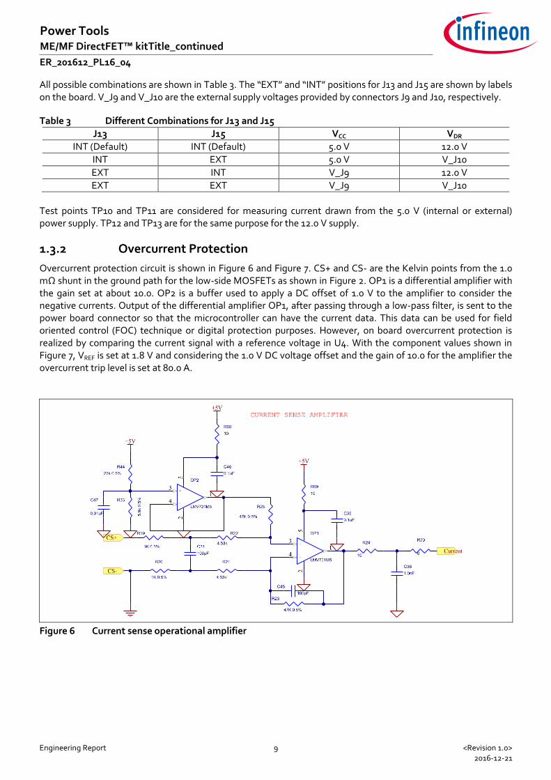
1.3.2 Overcurrent Protection
Overcurrent protection circuit is shown in Figure 6 and Figure 7. CS+ and CS- are the Kelvin points from the 1.0 mΩ shunt in the ground path for the low-side MOSFETs as shown in Figure 2. OP1 is a differential amplifier with the gain set at about 10.0. OP2 is a buffer used to apply a DC offset of 1.0 V to the amplifier to consider the negative currents. Output of the differential amplifier OP1, after passing through a low-pass filter, is sent to the power board connector so that the microcontroller can have the current data. This data can be used for field oriented control (FOC) technique or digital protection purposes. However, on board overcurrent protection is realized by comparing the current signal with a reference voltage in U4. With the component values shown in Figure 7, VREF is set at 1.8 V and considering the 1.0 V DC voltage offset and the gain of 10.0 for the amplifier the overcurrent trip level is set at 80.0 A.
Figure 6 Current sense operational amplifier
Engineering Report 10 <Revision 1.0> 2016-12-21
Power Tools ME/MF DirectFET™ kitTitle_continued
ER_201612_PL16_04
Figure 7 Current shutdown circuitry (SD)
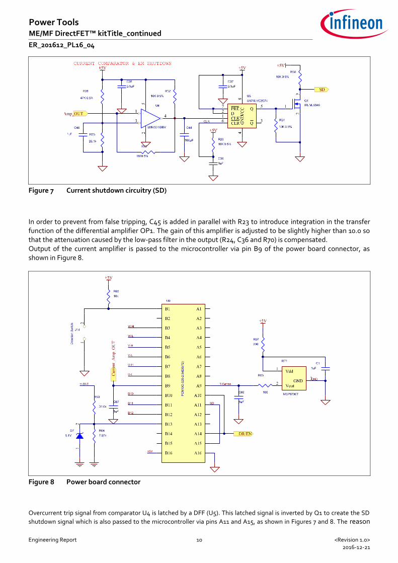
In order to prevent from false tripping, C45 is added in parallel with R23 to introduce integration in the transfer function of the differential amplifier OP1. The gain of this amplifier is adjusted to be slightly higher than 10.0 so that the attenuation caused by the low-pass filter in the output (R24, C36 and R70) is compensated. Output of the current amplifier is passed to the microcontroller via pin B9 of the power board connector, as shown in Figure 8.
Figure 8 Power board connector
Overcurrent trip signal from comparator U4 is latched by a DFF (U5). This latched signal is inverted by Q1 to create the SD
shutdown signal which is also passed to the microcontroller via pins A11 and A15, as shown in Figures 7 and 8. The reason
Engineering Report 11 <Revision 1.0> 2016-12-21
Power Tools ME/MF DirectFET™ kitTitle_continued
ER_201612_PL16_04 why 2 pins have been used for this signal is so that both XMCTM1300 and XMCTM4400 Drive Cards could be used with this demo board.
1.3.3 Over-Temperature Protection
MCP9700, an analogue temperature sensor, in an SOT-23 package is soldered on the PCB close to the heatsink to measure the temperature of the board as shown in Figure 3. This sensor converts temperature to voltage with a 0.5 V offset at 0.0 ˚C and a 10.0 mV/˚C temperature coefficient, as shown in Figure 9. In order to suppress the switching noise at the output of the sensor due to BLDC motor operation, low pass filters are used both in the VDD and in the output path. Output voltage is connected to the microcontroller via pin A9 of the power board connector as shown in Figure 8.
Figure 9 Output voltage vs. temperature for MCP9700
1.3.4 Gate Drivers
Infineon’s 2EDL05N06PF half-bridge MOSFET gate driver IC has been used for each phase in this demo board. Gate driver circuit for phase U is shown in Figure 10. U-H and U-L are PWM control signals from the microcontroller for phase U high-side and low-side MOSFETs, respectively.
Figure 10 Gate driver circuit for each phase
Engineering Report 12 <Revision 1.0> 2016-12-21
Power Tools ME/MF DirectFET™ kitTitle_continued
ER_201612_PL16_04 During normal operation of the circuit, SD is high which allows the PWM signals (U-H and U-L for phase U) to pass through the gate driver. U-HO and U-LO are the outputs of the gate driver which are connected to gate resistors of high-side and low-side MOSFETs in phase U, respectively. SD signal is created in overcurrent protection circuit explained previously and shown in Figure 6 and Figure 7. However, the microcontroller also has control of this signal. There is a driver enable signal (𝐷𝑅 − 𝐸𝑁 ) coming from the microcontroller via pin A10 ( Figure 8) that can override the logic of SD signal to disable the gate drivers. In normal operation of the circuit, (𝐷𝑅 − 𝐸𝑁 ) is low which turns on EN-LED D1 shown in Figure 11. The position of this LED is shown in Figure 3. So, in normal conditions, Q25 is off and SD signal is pulled up by R41, as shown in Figure 11.
Figure 11 Drive-enable circuit
Whenever an overcurrent trip occurs or (𝐷𝑅 − 𝐸𝑁 ) is set high by microcontroller, the shut-down signal SD goes low which turns off all the MOSFETs in the three phase inverter.
1.3.5 Heatsink and Gap Pad
One important advantage of DirectFETTMs is the capability of top-side cooling using a heatsink. An aluminium heatsink from Alpha (UB45) has been customized for our power board. As shown in Figure 12, this heatsink can be ordered with different base thicknesses and fin heights.
Figure 12 UB45 Aluminium heatsink series
Engineering Report 13 <Revision 1.0> 2016-12-21
Power Tools ME/MF DirectFET™ kitTitle_continued
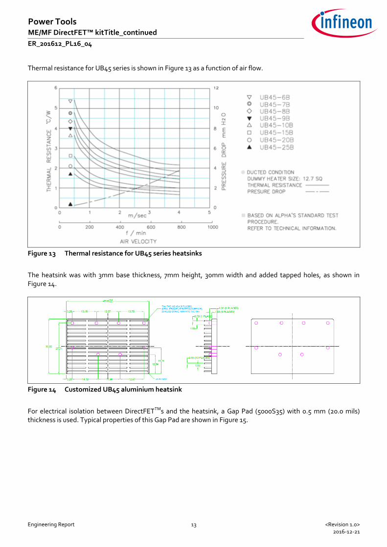
ER_201612_PL16_04 Thermal resistance for UB45 series is shown in Figure 13 as a function of air flow.
Figure 13 Thermal resistance for UB45 series heatsinks
The heatsink was with 3mm base thickness, 7mm height, 30mm width and added tapped holes, as shown in Figure 14.
Figure 14 Customized UB45 aluminium heatsink
For electrical isolation between DirectFETTMs and the heatsink, a Gap Pad (5000S35) with 0.5 mm (20.0 mils) thickness is used. Typical properties of this Gap Pad are shown in Figure 15.
Engineering Report 14 <Revision 1.0> 2016-12-21
Power Tools ME/MF DirectFET™ kitTitle_continued
ER_201612_PL16_04
Figure 15 Typical Properties for Gap Pad 5000S35
The available thicknesses for Gap Pad 5000S35 are shown in Figure 16 as a function of thermal resistance.
Figure 16 Available Thicknesses for Gap Pad 5000S5 as a function of thermal resistance
Engineering Report 15 <Revision 1.0> 2016-12-21
Power Tools ME/MF DirectFET™ kitTitle_continued
ER_201612_PL16_04
In order to make sure that the Gap Pad is not mechanically overstressed, the torque level of 0.9 Nm to 1.1 Nm should be applied to tighten the screws of the heatsink. The drawing for the Gap Pad is shown in Figure 17.
Figure 17 Drawing for the customized Gap Pad 5000S5
Engineering Report 16 <Revision 1.0> 2016-12-21
Power Tools ME/MF DirectFET™ kitTitle_continued
ER_201612_PL16_04 1.4 System Power Up
It should be noted that this three phase demo board is not a stand-alone solution to run a BLDC motor. It requires an XMCTM1300 (or an XMCTM4400) Drive Card as the controller board. Figure 18 shows the three-phase demo board (right-side) connected to an XMCTM1300 Drive Card (left-side).
Input
Terminals
Hall
Inputs
XMCTM
1300 Drive Card Three Phase Demo
Board
Output Terminals
Figure 18 Three-Phase Demo Board Connected to XMCTM1300 Drive Card
The software description will be provided in a separate section but for now it is assumed that the XMCTM Drive Card is already loaded with the required code and ready to be used. Note: The controller board In this Kit is being delivered with the software loaded in “Hall learning mode” and default parameters. For full motor control, new Hall parameters need to be added in the code, the Learning Mode disabled, and the controller re-programmed with this modified code. Please see sections 1.5.4 and 2 for insertion of new Hall parameters in code and subsequent re-programming instructions. The following order is recommended to run the board:
1. Output phases are connected to the BLDC motor. Order is not important when in Hall Learning Mode.
2. BLDC Hall sensors are directly connected to the Hall X101 connector in the XMCTM1300 Drive Card. Order
of Hall sensor inputs (pins 2, 3,and 4 only) is not important when in Hall Learning Mode. However, as
shown in Table 1.1, pin1 is GND and pin5 is VDD (+5V).
3. XMCTM Drive Card is connected to the demo board through the power board connector;
4. For using the on-board power supplies, jumpers of J13 and J15 should be on “INT” positions.
5. In case of using external power supplies, they should be connected to J9 and J10 and make sure that
jumpers of J13 and J15 are on “EXT” positions;
6. Input power supply (20.0 V typical) or 18.0 V battery should be connected to J1 (+) and J2 (-). It is
recommended to use short cables for the input power supply to limit the ripple current passing through
the input bulk capacitors. Additional input capacitors could be used close to the board, if long cables are
used.
7. If programming or in “Hall Learning Mode” a USB to micro USB cable has to be connected from
computer to connector X202 on the controller board.
Please refer to Figure 3 and Figure 4 for the position of the connectors and jumpers in the demo board.
Engineering Report 17 <Revision 1.0> 2016-12-21
Power Tools ME/MF DirectFET™ kitTitle_continued
ER_201612_PL16_04 1.5 Getting Started with the Infineon Power Tools DirectFETTM Kit
1.5.1 Getting Started with DAVETM (Version 4)
DAVETM is an Infineon free of charge Eclipse based IDE using a GNU C-compiler providing extensive, configurable, and reusable code repository for XMC™ industrial microcontroller powered by ARM® Cortex®-M processors. DAVETM installation package is provided in www.infineon.com/DAVE and all the documentation necessary for installation and quick start can be downloaded from the same webpage. As reference guides, the user is advised to refer to the documents (Infineon Technologies AG, 2016) and (Infineon Technologies AG, 2015)
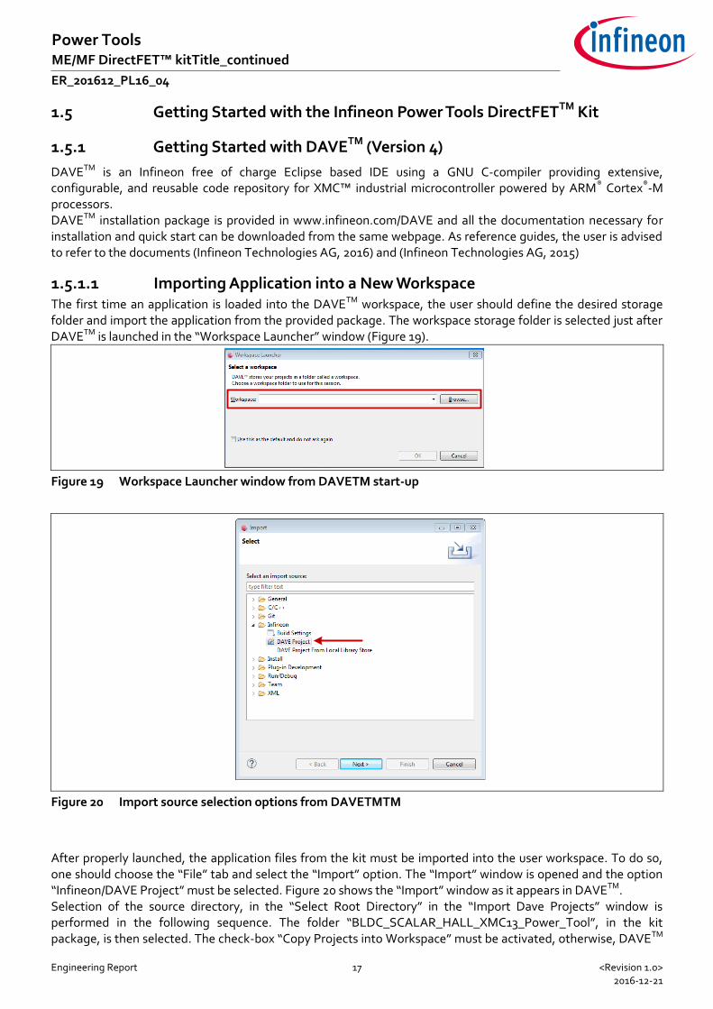
1.5.1.1 Importing Application into a New Workspace The first time an application is loaded into the DAVETM workspace, the user should define the desired storage folder and import the application from the provided package. The workspace storage folder is selected just after DAVETM is launched in the “Workspace Launcher” window (Figure 19).
Figure 19 Workspace Launcher window from DAVETM start-up
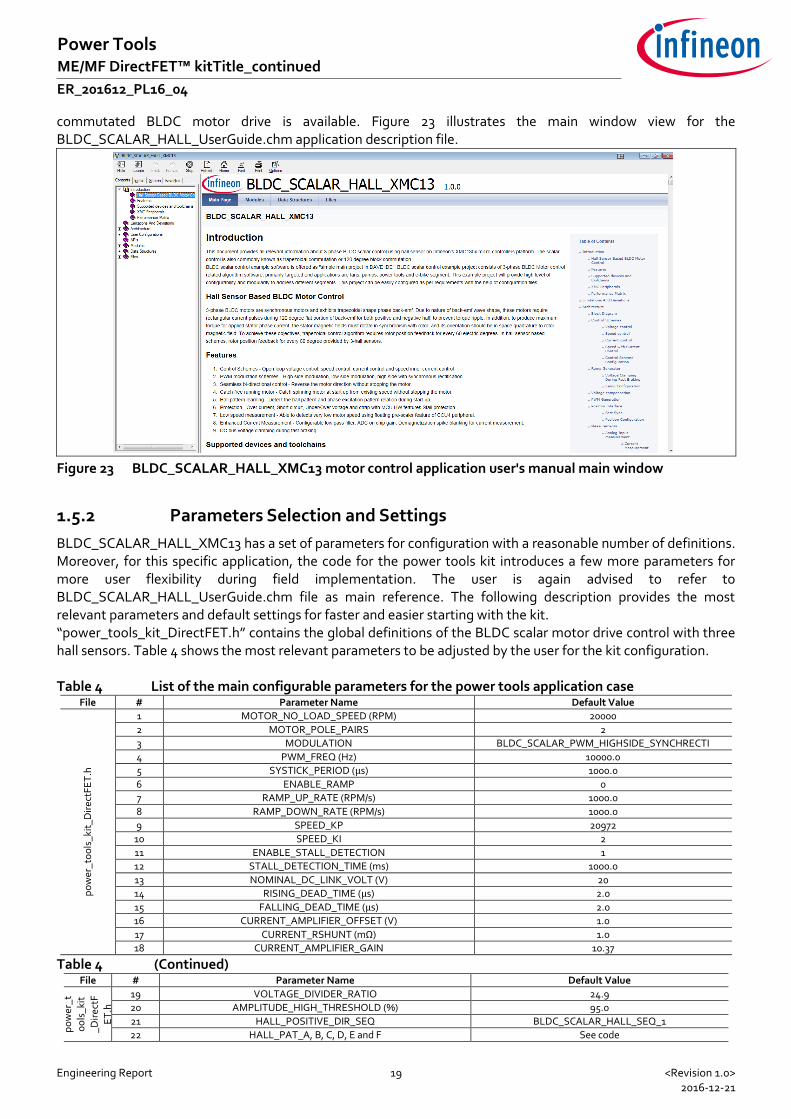
Figure 20 Import source selection options from DAVETMTM
After properly launched, the application files from the kit must be imported into the user workspace. To do so, one should choose the “File” tab and select the “Import” option. The “Import” window is opened and the option “Infineon/DAVE Project” must be selected. Figure 20 shows the “Import” window as it appears in DAVETM. Selection of the source directory, in the “Select Root Directory” in the “Import Dave Projects” window is performed in the following sequence. The folder “BLDC_SCALAR_HALL_XMC13_Power_Tool”, in the kit package, is then selected. The check-box “Copy Projects into Workspace” must be activated, otherwise, DAVETM
Engineering Report 18 <Revision 1.0> 2016-12-21
Power Tools ME/MF DirectFET™ kitTitle_continued
ER_201612_PL16_04 will use the source files in the kit package and all the modifications will overwrite the original files. Figure 21 illustrates the “Import Dave Projects” window for source file directory selection.
Figure 21 Import DAVETM Projects window for source files selection
1.5.1.2 DAVETM IDE Perspective As soon as the application is properly loaded in DAVETM, user is able to access all the configuration files, routines and interrupt service routines (which are part of the BLDC drive for power tools applications) via DAVETM main window (Figure 22). Basically, the digital control method is developed most completely in C-Language and uses GNU C-Compiler for creating the executable file to be loaded into the microcontroller flash memory.
Figure 22 DAVETM main window
In the project explorer window, the user has access to the BLDC_SCALAR_HALL_XMC13 application description. The full documentation about the general algorithm which implements the scalar speed control for a block
Engineering Report 19 <Revision 1.0> 2016-12-21
Power Tools ME/MF DirectFET™ kitTitle_continued
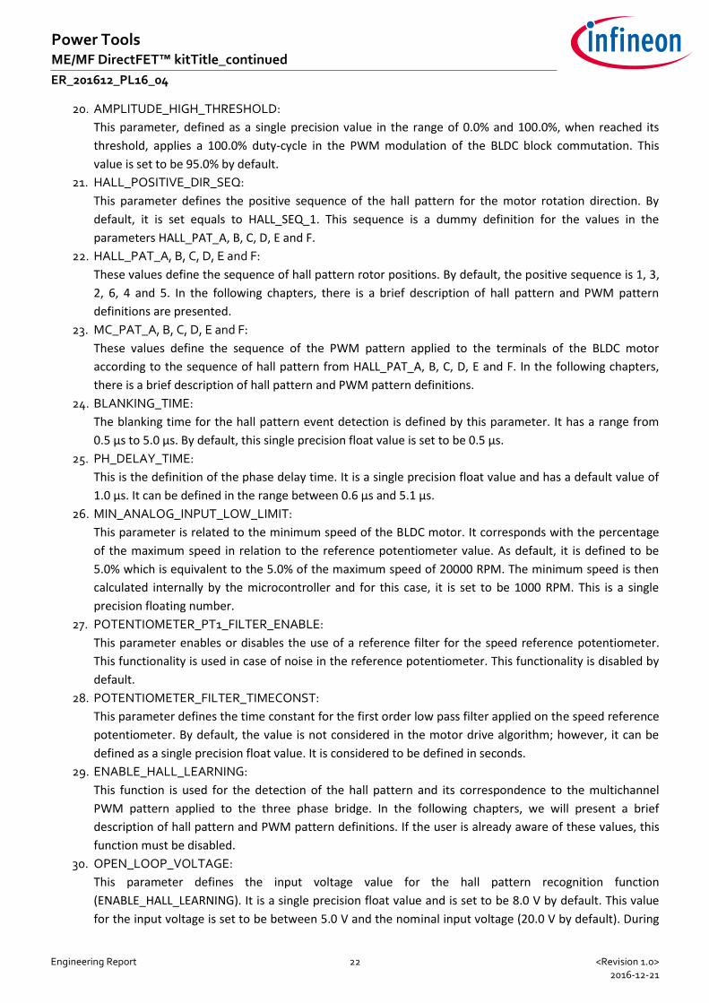
ER_201612_PL16_04 commutated BLDC motor drive is available. Figure 23 illustrates the main window view for the BLDC_SCALAR_HALL_UserGuide.chm application description file.
Figure 23 BLDC_SCALAR_HALL_XMC13 motor control application user's manual main window
1.5.2 Parameters Selection and Settings
BLDC_SCALAR_HALL_XMC13 has a set of parameters for configuration with a reasonable number of definitions. Moreover, for this specific application, the code for the power tools kit introduces a few more parameters for more user flexibility during field implementation. The user is again advised to refer to BLDC_SCALAR_HALL_UserGuide.chm file as main reference. The following description provides the most relevant parameters and default settings for faster and easier starting with the kit. “power_tools_kit_DirectFET.h” contains the global definitions of the BLDC scalar motor drive control with three hall sensors. Table 4 shows the most relevant parameters to be adjusted by the user for the kit configuration. Table 4 List of the main configurable parameters for the power tools application case
File # Parameter Name Default Value
po
wer
_to
ols
_kit
_Dir
ectF
ET
.h
1 MOTOR_NO_LOAD_SPEED (RPM) 20000
2 MOTOR_POLE_PAIRS 2
3 MODULATION BLDC_SCALAR_PWM_HIGHSIDE_SYNCHRECTI
4 PWM_FREQ (Hz) 10000.0
5 SYSTICK_PERIOD (µs) 1000.0
6 ENABLE_RAMP 0
7 RAMP_UP_RATE (RPM/s) 1000.0
8 RAMP_DOWN_RATE (RPM/s) 1000.0
9 SPEED_KP 20972
10 SPEED_KI 2
11 ENABLE_STALL_DETECTION 1
12 STALL_DETECTION_TIME (ms) 1000.0
13 NOMINAL_DC_LINK_VOLT (V) 20
14 RISING_DEAD_TIME (µs) 2.0
15 FALLING_DEAD_TIME (µs) 2.0
16 CURRENT_AMPLIFIER_OFFSET (V) 1.0
17 CURRENT_RSHUNT (mΩ) 1.0
18 CURRENT_AMPLIFIER_GAIN 10.37
Table 4 (Continued) File # Parameter Name Default Value
This is the parameter which defines directly the maximum no-load speed presented by the BLDC rotor. It
is an unsigned integer type variable and it is defined in RPM values. The default value is set to be 20000.0
RPM.
2. MOTOR_POLE_PAIRS:
It defines the number of pole-pairs of the machine rotor. It is a unsigned integer number and presents 2
as default value.
3. MODULATION:
It selects the type of modulation used for the generation of the BLDC block commutation pulses. For the
power tools application, the user has only two configurations: BLDC_SCALAR_PWM_HIGHSIDE for
standard PWM block commutation and BLDC_SCALAR_PWM_HIGHSIDE_SYNCHRECTI for BLDC block
commutation with synchronous rectification.
4. PWM_FREQ:
This parameter defines the switching frequency in Hz to be applied in the PWM block commutation of the
BLDC machine. For this case, the user can have as an input a single precision float input. The range of
operation of the switching is not allowed to be outside the interval between 1.0 kHz and 100.0 kHz. As a
default value, 10.0 kHz is used.
5. SYSTICK_PERIOD:
SYSTICK defines the period in which the system state machine runs inside the microcontroller. It is also
defined in a single precision floating point type value and its range can be set from 1000.0 μs to 10000.0
μs. 1.0 ms is the default value for the state machine call function.
6. ENABLE_RAMP:
It defines the enable signal for the ramp-up of the motor speed. Enabling the ramp-up option, a linear
function is defined to increase the speed reference from 0 RPM to a value set by the speed reference
potentiometer. By default, the ramp-up function is disabled.
7. RAMP_UP_RATE:
This value defines the ramp-up rate from an increase in the speed reference defined by the speed
reference potentiometer. Due to the fact the ramp function is not enabled by default, this parameter is
not considered.
8. RAMP_DOWN_RATE:
This value defines the ramp-down rate from a decrease in the speed reference defined by the speed
reference potentiometer. Due to the fact the ramp function is not enabled by default, this parameter is
not considered.
9. SPEED_KP:
Engineering Report 21 <Revision 1.0> 2016-12-21
Power Tools ME/MF DirectFET™ kitTitle_continued
ER_201612_PL16_04
The Proportional-Integral (PI) controller has the proportional gain defined by this parameter. As the
calculation of the PI is performed using fixed-point operation, this parameter is defined in Q15 base.
10. SPEED_KI:
The Proportional-Integral (PI) controller has the integration gain defined by this parameter. As the
calculation of the PI is performed using fixed-point operation, this parameter is defined in Q15 base.
11. ENABLE_STALL_DETECTION:
The stall detection is enabled by ENABLE_STALL_DETECTION. In case the stall detection is enabled, the
rotor is going to be allowed to operate, for a certain period of a time, with its rotor locked. By default, this
functionality is enabled.
12. STALL_DETECTION_TIME:
It defines the period of time that the rotor is allowed to operate in stall operation, meaning the amount
of time that the motor, even with its rotor locked, is still operating. This value is set by a single precision
float type value in milliseconds. By default, its value is set to be 1000.0 ms (1.0 s).
13. NOMINAL_DC_LINK_VOLT:
This parameter is used to define the nominal input voltage of the inverter 6-switches inverter bridge. It is
defined using a single precision float value and has a default value equal to 20.0 V. The “Power Tools
DirectFETTM Kit” is equipped with Infineon IRF7480 which is a 40.0 V device. The user must be aware of
the input voltage selection for possible protection of the switching devices in the board.
14. RISING_DEAD_TIME:
This parameter defines the dead-time for the rising edge of the PWM pulse. It is also a single precision
float value and has a default value of 2.0 μs.
15. FALLING_DEAD_TIME:
This parameter defines the dead-time for the falling edge of PWM pulse. It is also a single precision float
value and has a default value of 2.0 μs.
16. CURRENT_AMPLIFIER_OFFSET:
The current measurement is performed via a single-shunt configuration connected to the DC input of the
6-switches inverter bridge. In order to avoid negative voltage levels at the input of the microcontroller
analogue to digital converter (ADC), a level shift is applied to the resistor shunt differential output signal
via operational amplifier circuitry. CURRENT_AMPLIFIER_OFFSET defines the hardware DC level shift
applied on the DC current measurement. It is a single precision float value and has default value
approximately equals to 1.0 V.
17. CURRENT_RSHUNT:
This parameter defines the shunt value, in mΩ, of the DC current measurement circuitry (RS1). It is a single
precision float value and has a default value of 1.0 mΩ as it is presented by the power board circuitry.
18. CURRENT_AMPLIFIER_GAIN:
The DC current amplifier gain is defined by the hardware. For the microcontroller internal measurement
and proper scaling factor, this parameter has to be defined, otherwise, the interface with μCProbe will
present mismatches in the streamed variables. This parameter has a default value of approximately 10.37
and it is calculated by the ration between the resistors R23 and R21 or R22. This parameter also requires a
single precision floating point type value.
19. VOLTAGE_DIVIDER_RATIO:
The input voltage is monitored by the microcontroller and streamed via serial connection using the
μCProbe. This voltage value, most likely with a larger value than the microcontroller ADC reference (5.0 V)
(20.0 V as default value), is stepped-down, by a simple voltage divider (R63 and R64). As default value, this
ratio is set to be approximately 4.02. This parameter also requires a single precision float point type value.
Engineering Report 22 <Revision 1.0> 2016-12-21
Power Tools ME/MF DirectFET™ kitTitle_continued
ER_201612_PL16_04
20. AMPLITUDE_HIGH_THRESHOLD:
This parameter, defined as a single precision value in the range of 0.0% and 100.0%, when reached its
threshold, applies a 100.0% duty-cycle in the PWM modulation of the BLDC block commutation. This
value is set to be 95.0% by default.
21. HALL_POSITIVE_DIR_SEQ:
This parameter defines the positive sequence of the hall pattern for the motor rotation direction. By
default, it is set equals to HALL_SEQ_1. This sequence is a dummy definition for the values in the
parameters HALL_PAT_A, B, C, D, E and F.
22. HALL_PAT_A, B, C, D, E and F:
These values define the sequence of hall pattern rotor positions. By default, the positive sequence is 1, 3,
2, 6, 4 and 5. In the following chapters, there is a brief description of hall pattern and PWM pattern
definitions are presented.
23. MC_PAT_A, B, C, D, E and F:
These values define the sequence of the PWM pattern applied to the terminals of the BLDC motor
according to the sequence of hall pattern from HALL_PAT_A, B, C, D, E and F. In the following chapters,
there is a brief description of hall pattern and PWM pattern definitions.
24. BLANKING_TIME:
The blanking time for the hall pattern event detection is defined by this parameter. It has a range from
0.5 μs to 5.0 μs. By default, this single precision float value is set to be 0.5 μs.
25. PH_DELAY_TIME:
This is the definition of the phase delay time. It is a single precision float value and has a default value of
1.0 μs. It can be defined in the range between 0.6 μs and 5.1 μs.
26. MIN_ANALOG_INPUT_LOW_LIMIT:
This parameter is related to the minimum speed of the BLDC motor. It corresponds with the percentage
of the maximum speed in relation to the reference potentiometer value. As default, it is defined to be
5.0% which is equivalent to the 5.0% of the maximum speed of 20000 RPM. The minimum speed is then
calculated internally by the microcontroller and for this case, it is set to be 1000 RPM. This is a single
precision floating number.
27. POTENTIOMETER_PT1_FILTER_ENABLE:
This parameter enables or disables the use of a reference filter for the speed reference potentiometer.
This functionality is used in case of noise in the reference potentiometer. This functionality is disabled by
default.
28. POTENTIOMETER_FILTER_TIMECONST:
This parameter defines the time constant for the first order low pass filter applied on the speed reference
potentiometer. By default, the value is not considered in the motor drive algorithm; however, it can be
defined as a single precision float value. It is considered to be defined in seconds.
29. ENABLE_HALL_LEARNING:
This function is used for the detection of the hall pattern and its correspondence to the multichannel
PWM pattern applied to the three phase bridge. In the following chapters, we will present a brief
description of hall pattern and PWM pattern definitions. If the user is already aware of these values, this
function must be disabled.
30. OPEN_LOOP_VOLTAGE:
This parameter defines the input voltage value for the hall pattern recognition function
(ENABLE_HALL_LEARNING). It is a single precision float value and is set to be 8.0 V by default. This value
for the input voltage is set to be between 5.0 V and the nominal input voltage (20.0 V by default). During
Engineering Report 23 <Revision 1.0> 2016-12-21
Power Tools ME/MF DirectFET™ kitTitle_continued
ER_201612_PL16_04
this operation, the motor is controlled in open loop condition. By then, the user is advised to define a
lower value for the input for avoiding large values for phase currents.
31. OPEN_LOOP_SPEED:
This parameter represents a fraction of the no-load maximum speed for operation of the BLDC motor
drive during open loop condition for hall pattern identification mode. ). It is a single precision float value
and is set to be 5.0% by default, which represents a fraction of 5.0% (1000 RPM) of the maximum set no-
load speed (20000 RPM).
32. TEMEPRATURE_SHUTDOWN_THRESHOLD:
This is the threshold level for the power board temperature, in °C, above which the inverter stops
operating. It is an integer value and used as a reference to compare with the board temperature
measured by the MCP9700T sensor. This parameter has a default value of 80°C.
33. TEMPERATURE_HYSTERESIS:
This is the value for the power board temperature, in °C, above which the inverter will not start. This is an
additional temperature protection to force the user not to start the power tool at an already high
temperature condition. It is an integer number with a default value of 50°C.
1.5.3 Compilation and Debug Session
After configuring the parameters in Table 4, when required, the code must be compiled and loaded into the XMCTM1302 flash memory via the Segger J-Link Programmer/Debbuger. This device is already present in the KIT_XMC1300_DC_V1 Infineon Kit. For compiling the code, the user must access the “Project” instance from the main tab menu and click on the “Build Project” option, as it is illustrated in Figure 24 “Build All” and “Clean” options can also be used. For more details on the compilation option of DAVETM, the user is advised to refer to (Infineon Technologies AG, 2016) and (Infineon Technologies AG, 2015).
Figure 24 “Build Project” (code compilation) functionality of DAVE™
For loading the code into the device internal flash, the Segger J-Link Programmer/Debbuger is used. The debugger must be connected to the computer via USB cable. The power board should properly be powered. When the ENABLE_HALL_LEARNING is enabled, it is advised to apply 18.0 V or 20.0V and limit the input current from the external supply to 1A, since the BLDC motor drive during Learning operates in open loop.
Engineering Report 24 <Revision 1.0> 2016-12-21
Power Tools ME/MF DirectFET™ kitTitle_continued
ER_201612_PL16_04 The connection with debugger and the starting of the debug session is initiated by hitting the shortcut button indicated by the ”bug” image in DAVETM as shown in Figure 25.
Figure 25 Debug mode shortcut button from DAVETM
The debug session is followed by the “Debug Configurations”. The first time the debugger is initialized, the main window from Figure 26 is activated. Then, the user must select the Segger J-Link by double clicking on the option “GDB SEGGER J-Link Debugging”. After that, the “Debug” button is activated and the debug session is started automatically Figure 27.
ER_201612_PL16_04 1.5.4 Acquisition of Hall and Multichannel PWM Patterns
Initially, the sequence and relationship of the Hall sensors position with respect to the motor windings positons (Phases) is not known. Therefore it is necessary to run the motor with the loaded code as it comes pre-programmed in “Hall learning mode” as part of the kit. The macros represented by HALL_PAT_A, B, C, D, E and F are acquired directly from the hall sensors outputs at the connector X101. (as an alternative, one can manually rotate the rotor and measure the pattern with either an oscilloscope, or a simple multimeter). After the hall sequence is acquired, the macros HALL_PAT_A, B, C, D, E and F can be updated in the “power_tools_kit_DirectFET.h” file. For the acquisition of the multichannel PWM pattern, the system is configured to operate in open loop condition. Both duty-cycle and speed are predefined. The hall learning pattern recognition is enabled using the macro ENABLE_HALL_LEARNING from Table 4. DC voltage value and open-loop speed settings are defined in the definitions labelled as OPEN_LOOP_VOLTAGE and OPEN_LOOP_SPEED, respectively. After starting the debugging mode perspective, as described previously, the system can be resumed (play button) and, with the adaptive multichannel PWM pattern learning function enabled, the BLDC motor performs a few rotations and stops. After the rotor has stopped, the suspend mode can be triggered (pause button). Figure 28 shows the results for the multichannel PWM acquisition during motor start-up.
Hall
Phase U
High Side
Phase U
Low Side
Phase U
Current
Phase U
Figure 28 System waveforms for multichannel PWM pattern detection
With the system paused, the multichannel PWM pattern can be displayed in the “Expression” window. By selecting the “Expression” view in the “Show View” option of the “Window” tab, one can add any system variable. Figure 29 illustrates a screenshot of the debugging window perspective and activation of the “Expression” window.
Engineering Report 26 <Revision 1.0> 2016-12-21
Power Tools ME/MF DirectFET™ kitTitle_continued
ER_201612_PL16_04
Figure 29 Debugging mode view and "Expression" selection window
By adding the variable name MC_Pattern_DEBUG in the “Expression” window (Add new expression), the 6 multichannel PWM pattern states can be recognized directly from DAVETM. The first element must be disregarded, meaning that only the last six elements of the string MC_Pattern_DEBUG are necessary for the pattern recognition. The values of the MC_Pattern_DEBUG string are basically the values for the position interface (POSIF.MCM). For detailed description of operating modes of this peripheral, (Infineon Technologies AG, 2014) must be referenced. Converting MC_Pattern_DEBUG to hexadecimal and using the macros from the Table 5 and Table 6, the MC_PAT_A, B, C, D, E and F can be completed following the same sequence for the HALL_PAT_A, B, C, D, E and F. Hall learning procedure is explained in details in section 2.
Engineering Report 27 <Revision 1.0> 2016-12-21
Power Tools ME/MF DirectFET™ kitTitle_continued
ER_201612_PL16_04 1.6 System Operation
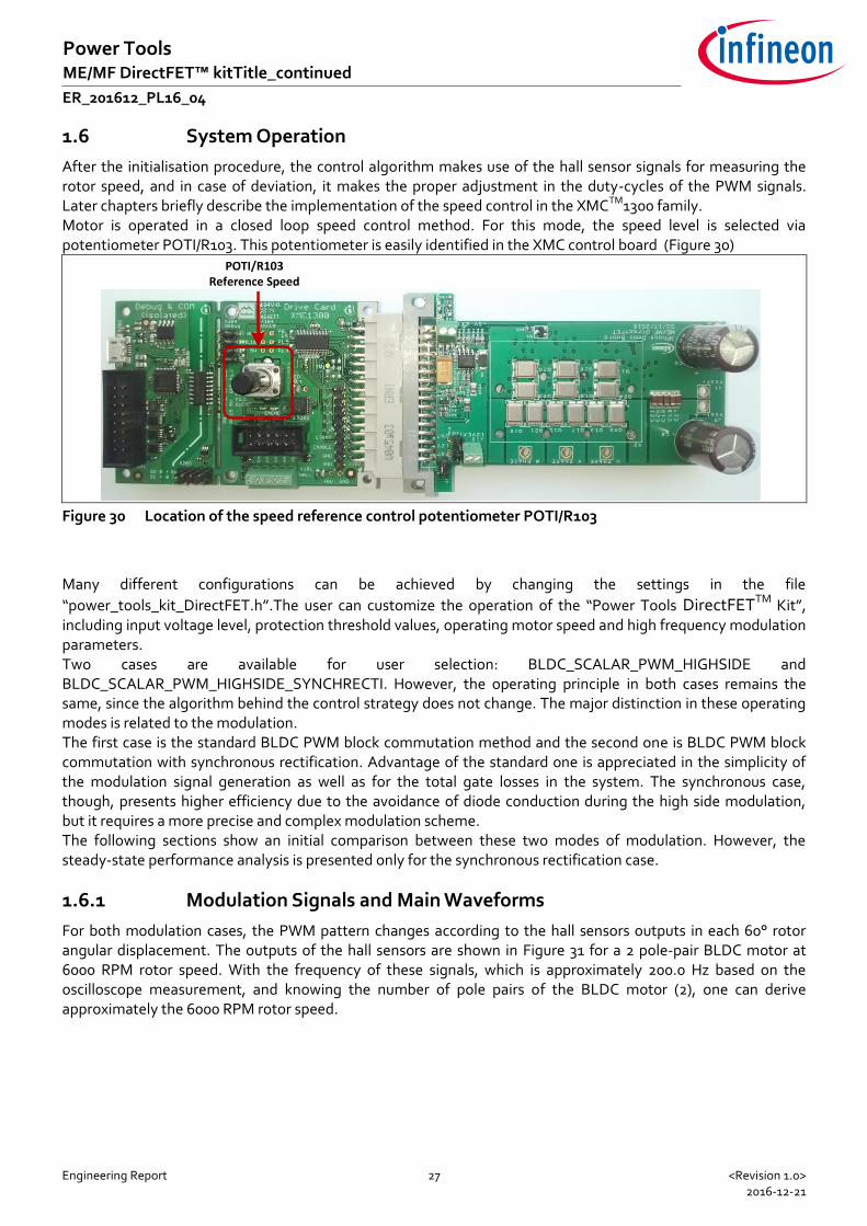
After the initialisation procedure, the control algorithm makes use of the hall sensor signals for measuring the rotor speed, and in case of deviation, it makes the proper adjustment in the duty-cycles of the PWM signals. Later chapters briefly describe the implementation of the speed control in the XMCTM1300 family. Motor is operated in a closed loop speed control method. For this mode, the speed level is selected via potentiometer POTI/R103. This potentiometer is easily identified in the XMC control board (Figure 30)
POTI/R103Reference Speed
Figure 30 Location of the speed reference control potentiometer POTI/R103
Many different configurations can be achieved by changing the settings in the file
“power_tools_kit_DirectFET.h”.The user can customize the operation of the “Power Tools DirectFETTM Kit”, including input voltage level, protection threshold values, operating motor speed and high frequency modulation parameters. Two cases are available for user selection: BLDC_SCALAR_PWM_HIGHSIDE and BLDC_SCALAR_PWM_HIGHSIDE_SYNCHRECTI. However, the operating principle in both cases remains the same, since the algorithm behind the control strategy does not change. The major distinction in these operating modes is related to the modulation. The first case is the standard BLDC PWM block commutation method and the second one is BLDC PWM block commutation with synchronous rectification. Advantage of the standard one is appreciated in the simplicity of the modulation signal generation as well as for the total gate losses in the system. The synchronous case, though, presents higher efficiency due to the avoidance of diode conduction during the high side modulation, but it requires a more precise and complex modulation scheme. The following sections show an initial comparison between these two modes of modulation. However, the steady-state performance analysis is presented only for the synchronous rectification case.
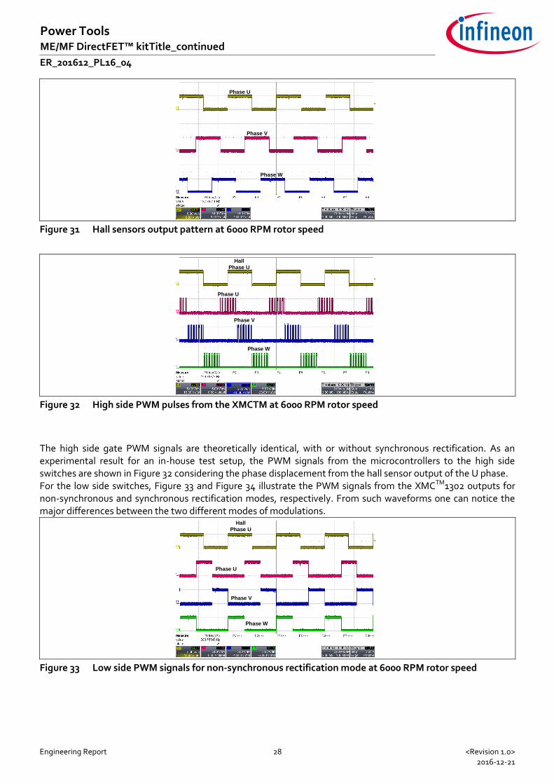
1.6.1 Modulation Signals and Main Waveforms
For both modulation cases, the PWM pattern changes according to the hall sensors outputs in each 60° rotor angular displacement. The outputs of the hall sensors are shown in Figure 31 for a 2 pole-pair BLDC motor at 6000 RPM rotor speed. With the frequency of these signals, which is approximately 200.0 Hz based on the oscilloscope measurement, and knowing the number of pole pairs of the BLDC motor (2), one can derive approximately the 6000 RPM rotor speed.
Engineering Report 28 <Revision 1.0> 2016-12-21
Power Tools ME/MF DirectFET™ kitTitle_continued
ER_201612_PL16_04
Phase U
Phase V
Phase W
Figure 31 Hall sensors output pattern at 6000 RPM rotor speed
Hall
Phase U
Phase U
Phase V
Phase W
Figure 32 High side PWM pulses from the XMCTM at 6000 RPM rotor speed
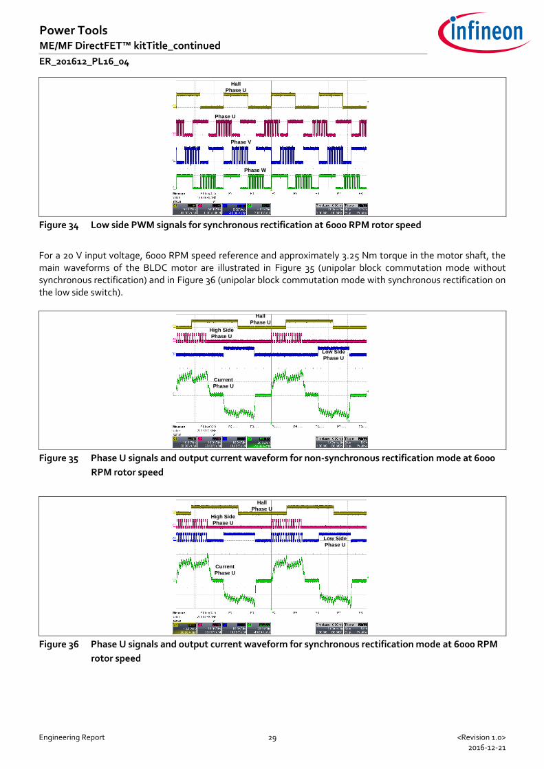
The high side gate PWM signals are theoretically identical, with or without synchronous rectification. As an experimental result for an in-house test setup, the PWM signals from the microcontrollers to the high side switches are shown in Figure 32 considering the phase displacement from the hall sensor output of the U phase. For the low side switches, Figure 33 and Figure 34 illustrate the PWM signals from the XMCTM1302 outputs for non-synchronous and synchronous rectification modes, respectively. From such waveforms one can notice the major differences between the two different modes of modulations.
Hall
Phase U
Phase U
Phase V
Phase W
Figure 33 Low side PWM signals for non-synchronous rectification mode at 6000 RPM rotor speed
Engineering Report 29 <Revision 1.0> 2016-12-21
Power Tools ME/MF DirectFET™ kitTitle_continued
ER_201612_PL16_04
Hall
Phase U
Phase U
Phase V
Phase W
Figure 34 Low side PWM signals for synchronous rectification at 6000 RPM rotor speed
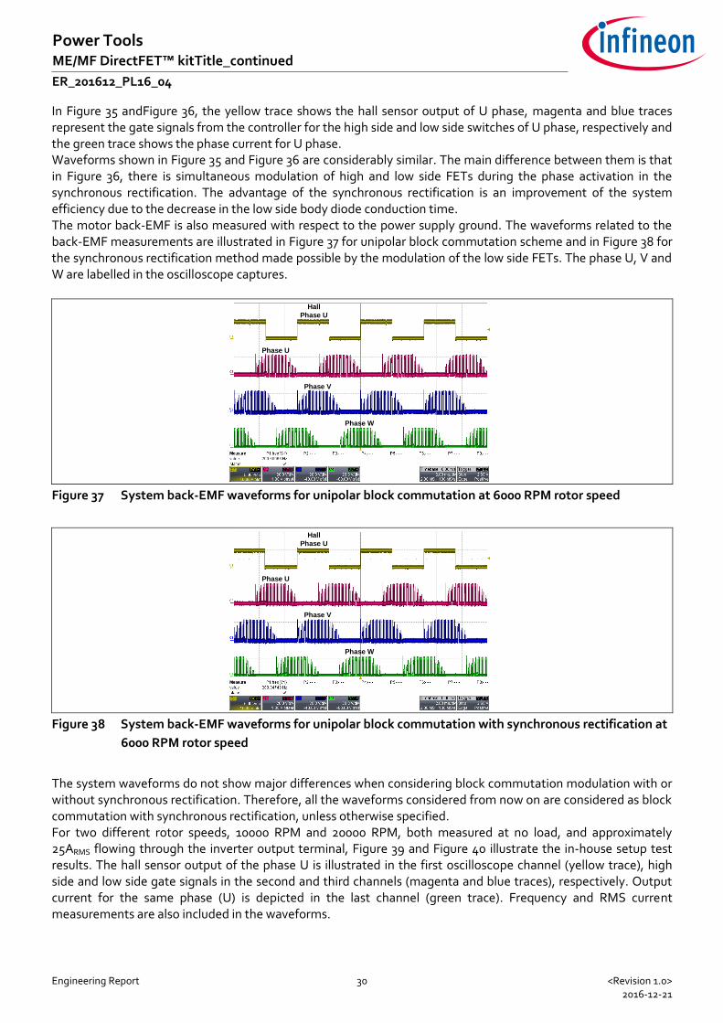
For a 20 V input voltage, 6000 RPM speed reference and approximately 3.25 Nm torque in the motor shaft, the main waveforms of the BLDC motor are illustrated in Figure 35 (unipolar block commutation mode without synchronous rectification) and in Figure 36 (unipolar block commutation mode with synchronous rectification on the low side switch).
Hall
Phase U
High Side
Phase U
Low Side
Phase U
Current
Phase U
Figure 35 Phase U signals and output current waveform for non-synchronous rectification mode at 6000
RPM rotor speed
Hall
Phase U
High Side
Phase U
Low Side
Phase U
Current
Phase U
Figure 36 Phase U signals and output current waveform for synchronous rectification mode at 6000 RPM
rotor speed
Engineering Report 30 <Revision 1.0> 2016-12-21
Power Tools ME/MF DirectFET™ kitTitle_continued
ER_201612_PL16_04 In Figure 35 andFigure 36, the yellow trace shows the hall sensor output of U phase, magenta and blue traces represent the gate signals from the controller for the high side and low side switches of U phase, respectively and the green trace shows the phase current for U phase. Waveforms shown in Figure 35 and Figure 36 are considerably similar. The main difference between them is that in Figure 36, there is simultaneous modulation of high and low side FETs during the phase activation in the synchronous rectification. The advantage of the synchronous rectification is an improvement of the system efficiency due to the decrease in the low side body diode conduction time. The motor back-EMF is also measured with respect to the power supply ground. The waveforms related to the back-EMF measurements are illustrated in Figure 37 for unipolar block commutation scheme and in Figure 38 for the synchronous rectification method made possible by the modulation of the low side FETs. The phase U, V and W are labelled in the oscilloscope captures.
Hall
Phase U
Phase U
Phase V
Phase W
Figure 37 System back-EMF waveforms for unipolar block commutation at 6000 RPM rotor speed
Hall
Phase U
Phase U
Phase V
Phase W
Figure 38 System back-EMF waveforms for unipolar block commutation with synchronous rectification at
6000 RPM rotor speed
The system waveforms do not show major differences when considering block commutation modulation with or without synchronous rectification. Therefore, all the waveforms considered from now on are considered as block commutation with synchronous rectification, unless otherwise specified. For two different rotor speeds, 10000 RPM and 20000 RPM, both measured at no load, and approximately 25ARMS flowing through the inverter output terminal, Figure 39 and Figure 40 illustrate the in-house setup test results. The hall sensor output of the phase U is illustrated in the first oscilloscope channel (yellow trace), high side and low side gate signals in the second and third channels (magenta and blue traces), respectively. Output current for the same phase (U) is depicted in the last channel (green trace). Frequency and RMS current measurements are also included in the waveforms.
Engineering Report 31 <Revision 1.0> 2016-12-21
Power Tools ME/MF DirectFET™ kitTitle_continued
ER_201612_PL16_04
Hall
Phase U
High Side
Phase U
Low Side
Phase U
Current
Phase U
Figure 39 Phase U signals and output current waveform for synchronous rectification mode at 10000 RPM
rotor speed and 25ARMS output current (5.0 Nm)
Hall
Phase U
High Side
Phase U
Low Side
Phase U
Current
Phase U
Figure 40 Phase U signals and output current waveform for synchronous rectification mode at 20000 RPM
rotor speed and 25ARMS output current (3.5 Nm)
At 10000 RPM, the duty-cycle is approximately 50.0% and the rotor frequency approximately matches the reference value set on the speed reference potentiometer. At 20000 RPM, due to saturation of the duty-cycle (100.0%), the rotor speed decreases to approximately 18500 RPM.
1.6.2 Overcurrent Protection
The “Power Tools DirectFETTM Kit” is equipped with a built-in hardware current protection circuitry formed by a DC shunt current measurement shutdown system. The trigger is selected via the analogue comparator and once latched, the gate signals are automatically disabled via digital AND gates. The microcontroller, as soon as the shutdown signal is identified, stops the motor operation. The current shutdown level is set to switch the system off by a current approximately equal to 90.0 A peak. Changes in the current level require hardware modification. Two tests are illustrated in Figure 41 and Figure 42. In both cases the phase currents are illustrated together with the shutdown signal (active low).
Engineering Report 32 <Revision 1.0> 2016-12-21
Power Tools ME/MF DirectFET™ kitTitle_continued
ER_201612_PL16_04
Phase Currents
U, V and W
Shutdown
Signal (SD)
Figure 41 Current shutdown protection operation at 10000RPM rotor speed (50% Duty-Cycle)
Phase Currents
U, V and W
Shutdown
Signal (SD)
Figure 42 Current shutdown protection operation at 20000RPM rotor speed (100% Duty-Cycle)
1.6.3 Temperature Protection
When the system reaches a defined temperature set by “TEMPERATURE_SHUTDOWN_THRESHOLD” from the file “power_tools_kit_DirectFET.h”, the gate pulses are automatically disabled. Such protection system is derived from an analogue-to-digital conversion of a voltage reading from the temperature sensor MCP9700T. Two tests have been performed: for rotor speed equal to 10000 RPM and 25.0 ARMS of load (5.0 Nm torque) and 10000 RPM and 25.0 ARMS of load (3.25 Nm torque). The monitored region is illustrated in the Figure 43.
Heatsink
Monitored
Area
Sensor
Monitored
Area
Figure 43 Monitored region for the heatsink temperature and sensor temperature data acquisition via a
thermal camera
Engineering Report 33 <Revision 1.0> 2016-12-21
Power Tools ME/MF DirectFET™ kitTitle_continued
ER_201612_PL16_04 The two tests are illustrated in Figure 44 andFigure 45. For these waveforms, the yellow trace (channel 1) represents the hall sensor output from phase U, the blue trace (channel 3) represents the shutdown signal from the microcontroller, the magenta trace (channel 2) represents sensor output and green trace (channel 4) illustrates the phase current. For both cases, the phase current was set to be approximately 25.0 ARMS.
Hall
Phase U
Current
Phase U
Shutdown
Signal
Sensor
Output
Figure 44 Temperature shutdown protection operation at 10000RPM rotor speed (50.0% Duty-Cycle/25.0
ARMS)
Hall
Phase U
Current
Phase U
Shutdown
Signal
Sensor
Output
Figure 45 Temperature shutdown protection operation at 20000RPM rotor speed (100.0% Duty-
Cycle/25.0 ARMS)
Considering the total time for temperature shutdown, the temperature data is recorded and illustrated in Figure 46 and Figure 47. For both cases, as seen in the recorded data, the shutdown acts when the sensor temperature is approximately 80°C. The time for system shutdown is about 4.5 minutes for 10000.0 RPM and about 4.0 minutes for 20000.0 RPM.
Engineering Report 34 <Revision 1.0> 2016-12-21
Power Tools ME/MF DirectFET™ kitTitle_continued
ER_201612_PL16_04
Figure 46 Temperature shutdown protection operation at 10000RPM rotor speed (50% Duty-Cycle/25.0
ARMS)
Figure 47 Temperature shutdown protection operation at 20000RPM rotor speed (100% Duty-Cycle/25.0
ARMS)
0 50 100 150 200 250 30020
30
40
50
60
70
80
90
100
t i me [s]
Tem
peratu
re
[oC
]
Heatsink Temperature
Sensor Temperature
0 50 100 150 200 250 30020
30
40
50
60
70
80
90
100
t i me [s]
Tem
peratu
re
[oC
]
Heatsink Temperature
Sensor Temperature
Engineering Report 35 <Revision 1.0> 2016-12-21
Power Tools ME/MF DirectFET™ kitTitle_continued
ER_201612_PL16_04 1.7 Operating Principle
The motor control algorithm implemented in the XMCTM1300 family is based on a speed control block commutation algorithm of the BLDC motor. The microcontroller has access to the terminal of three hall sensors, and according to the pattern generated from the combined output states, the proper switching sequence of the PWM signals are generated. In addition, input voltage, input current and temperature are digitized in order to provide protection means for safe operation of the motor. A simplified diagram of a two poles BLDC motor is illustrated in Figure 48 where the coils are displaced by 120°. No brushes are necessary, since the commutator is replaced by a six-switch bridge inverter (Figure 49)
Figure 48 Simplified diagram of a 2 poles BLDC motor
Figure 49 Simplified diagram of a 6-switch inverter bridge
By properly controlling the states of the MOSFETs in the inverter circuitry of Figure 49, one can precisely control the magnetic flux on the coils of the motor stator. Moreover, the speed of the rotor can be regulated by adjusting the PWM duty cycle. The speed is directly measured using thee hall sensors. With the pattern created by the output of this rotor positioning method, the control system is able to identify the proper PWM pattern which must be applied to the inverter switches. Depending on the hall pattern presented by the current position of the motor, the high side and low side of all phases are modulated. Considering the pattern shown in Figure 50, the output of the hall sensors (red traces and considering the phase U the LSB and phase W the MSB) can present the set 6, 4, 5, 1, 3, 2. POSIF0 and CCU8 of the XMCTM1300 family is going to create the PWM pattern (blue traces) using the multi-channel patterns 0x120, 0x 021, 0x201, 0,210, 0x012, 0x102, 0x120 for unipolar block commutation and 0x320, 0x 023, 0x203, 0,230, 0x032, 0x102, 0x320 for the case with synchronous rectification.
Engineering Report 36 <Revision 1.0> 2016-12-21
Power Tools ME/MF DirectFET™ kitTitle_continued
ER_201612_PL16_04
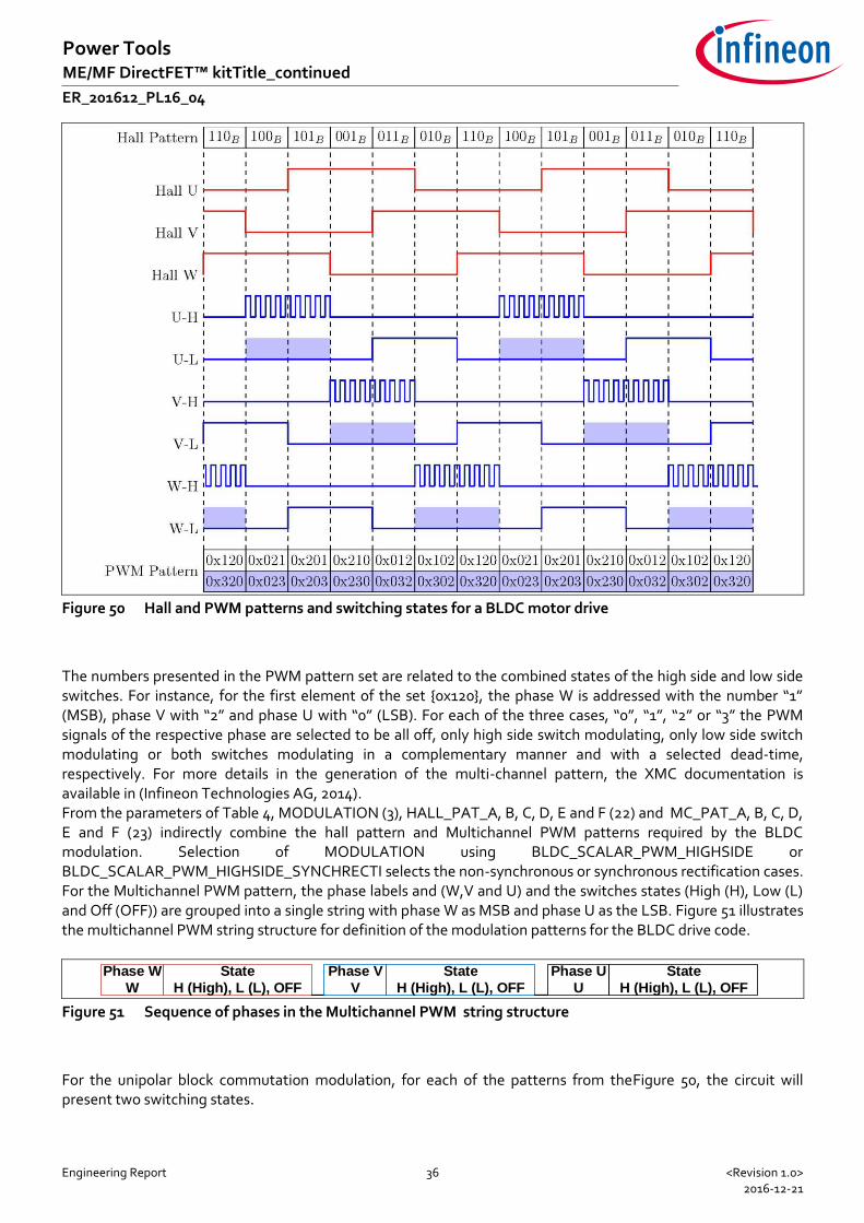
Figure 50 Hall and PWM patterns and switching states for a BLDC motor drive
The numbers presented in the PWM pattern set are related to the combined states of the high side and low side switches. For instance, for the first element of the set 0x120, the phase W is addressed with the number “1” (MSB), phase V with “2” and phase U with “0” (LSB). For each of the three cases, “0”, “1”, “2” or “3” the PWM signals of the respective phase are selected to be all off, only high side switch modulating, only low side switch modulating or both switches modulating in a complementary manner and with a selected dead-time, respectively. For more details in the generation of the multi-channel pattern, the XMC documentation is available in (Infineon Technologies AG, 2014). From the parameters of Table 4, MODULATION (3), HALL_PAT_A, B, C, D, E and F (22) and MC_PAT_A, B, C, D, E and F (23) indirectly combine the hall pattern and Multichannel PWM patterns required by the BLDC modulation. Selection of MODULATION using BLDC_SCALAR_PWM_HIGHSIDE or BLDC_SCALAR_PWM_HIGHSIDE_SYNCHRECTI selects the non-synchronous or synchronous rectification cases. For the Multichannel PWM pattern, the phase labels and (W,V and U) and the switches states (High (H), Low (L) and Off (OFF)) are grouped into a single string with phase W as MSB and phase U as the LSB. Figure 51 illustrates the multichannel PWM string structure for definition of the modulation patterns for the BLDC drive code.
Phase W
W
State
H (High), L (L), OFF
Phase V
V
State
H (High), L (L), OFF
Phase U
U
State
H (High), L (L), OFF Figure 51 Sequence of phases in the Multichannel PWM string structure
For the unipolar block commutation modulation, for each of the patterns from theFigure 50, the circuit will present two switching states.
Engineering Report 37 <Revision 1.0> 2016-12-21
Power Tools ME/MF DirectFET™ kitTitle_continued
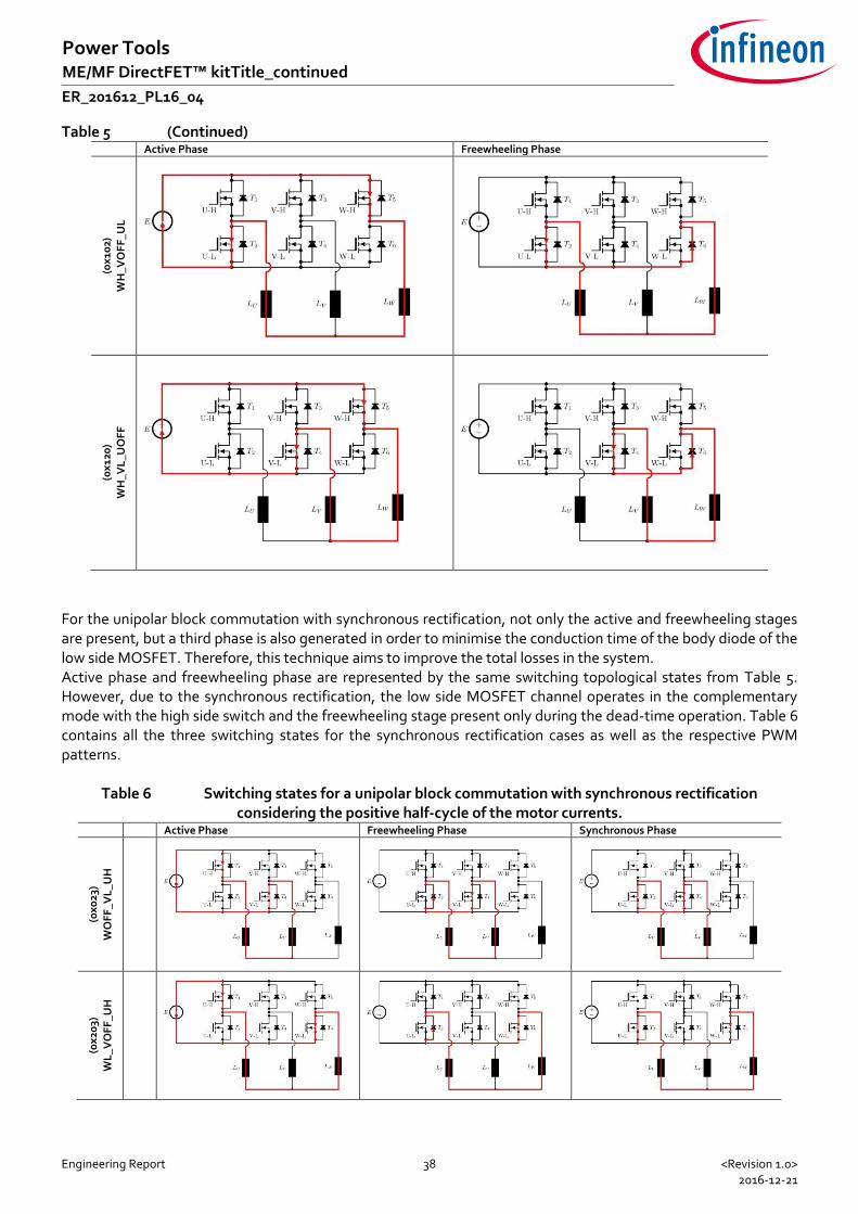
ER_201612_PL16_04 The active phase is selected when one of the high side switches of one of the phases is going to be activated. From the other two phases in the sequence, a low side switch is also kept in the active state. This stage represents the phase where the input supply is directly connected to the load. The freewheeling stage happens after the high side switch is turned off by grounding the respective gate signal. The body of the low side MOSFET of the same phase conducts the inductor current. All the switching states for the unipolar block commutation and the respective PWM pattern number are represented in Table 5. Table 5 Switching states for a unipolar block commutation considering the positive half-cycle of the
motor currents. Active Phase Freewheeling Phase
(0x
021
)
WO
FF
_VL
_UH
(0x
201)
WL
_VO
FF
_UH
(0x
210
)
WL
_VH
_UO
FF
(0x
012
)
WO
FF
_VH
_UL
Engineering Report 38 <Revision 1.0> 2016-12-21
Power Tools ME/MF DirectFET™ kitTitle_continued
ER_201612_PL16_04 Table 5 (Continued)
Active Phase Freewheeling Phase
(0x
102)
W
H_V
OF
F_U
L
(0x
120
) W
H_V
L_U
OF
F
For the unipolar block commutation with synchronous rectification, not only the active and freewheeling stages are present, but a third phase is also generated in order to minimise the conduction time of the body diode of the low side MOSFET. Therefore, this technique aims to improve the total losses in the system. Active phase and freewheeling phase are represented by the same switching topological states from Table 5. However, due to the synchronous rectification, the low side MOSFET channel operates in the complementary mode with the high side switch and the freewheeling stage present only during the dead-time operation. Table 6 contains all the three switching states for the synchronous rectification cases as well as the respective PWM patterns.
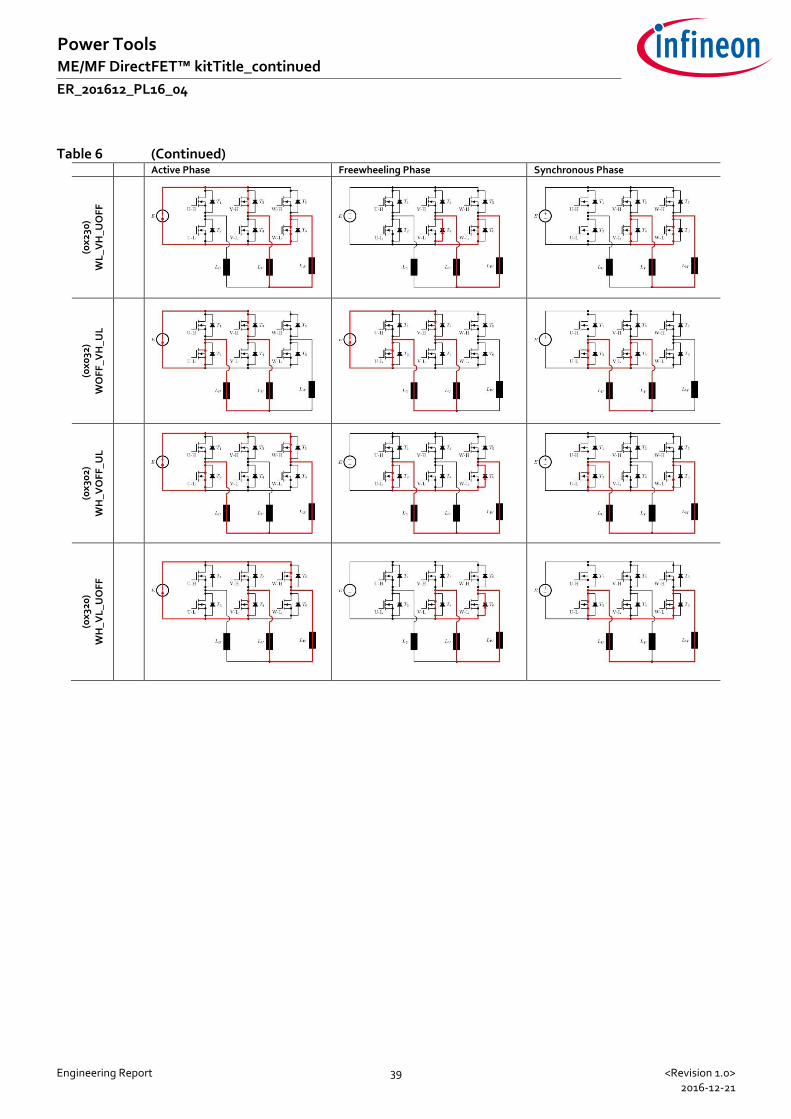
Table 6 Switching states for a unipolar block commutation with synchronous rectification considering the positive half-cycle of the motor currents.
Active Phase Freewheeling Phase Synchronous Phase
(0x
023
)
WO
FF
_VL
_UH
(0x
203)
WL
_VO
FF
_UH
Engineering Report 39 <Revision 1.0> 2016-12-21
Power Tools ME/MF DirectFET™ kitTitle_continued
ER_201612_PL16_04
Table 6 (Continued) Active Phase Freewheeling Phase Synchronous Phase
(0x
230
)
WL
_VH
_UO
FF
(0x
032
)
WO
FF
_VH
_UL
(0x
302)
WH
_VO
FF
_UL
(0x
320
)
WH
_VL
_UO
FF
Engineering Report 40 <Revision 1.0> 2016-12-21
Power Tools ME/MF DirectFET™ kitTitle_continued
ER_201612_PL16_04 1.8 Schematic and PCB layout:
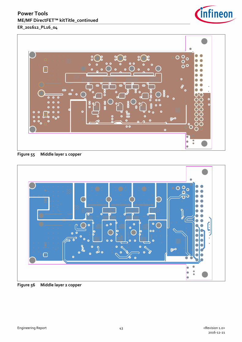
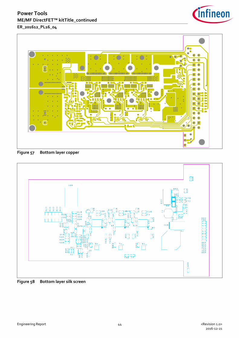
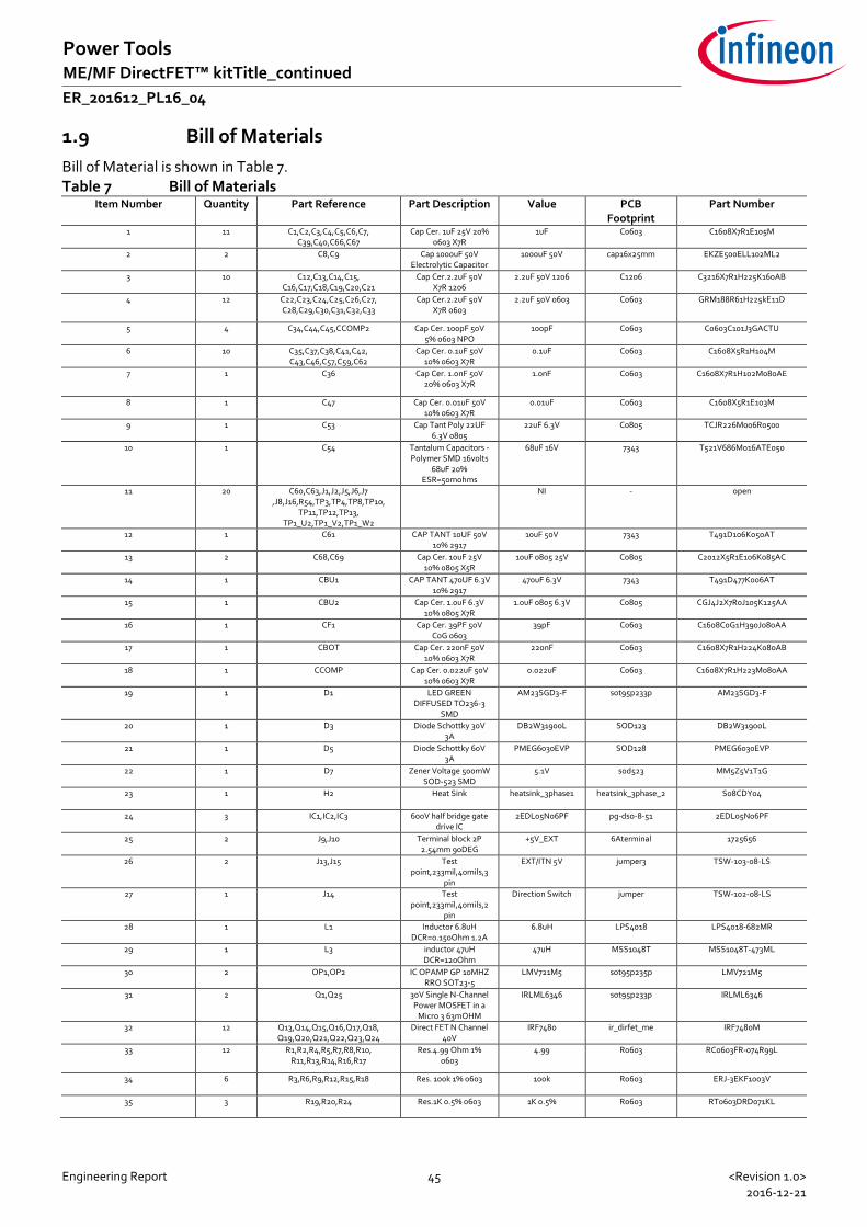
In this section the schematic and PCB layout for our demo board are provided. Figure 52 shows the schematic of the demo board. The PCB has 4 layers. The outer layers are 2 oz. copper and inner layers 1 oz. All layers are shown in Figure 53 to Figure 58, including silk screen for top and bottom layers.
Engineering Report 41 <Revision 1.0> 2016-12-21
Power Tools ME/MF DirectFET™ kitTitle_continued
ER_201612_PL16_04
Figure 52 Schematic of the demo board
Engineering Report 42 <Revision 1.0> 2016-12-21
Power Tools ME/MF DirectFET™ kitTitle_continued
ER_201612_PL16_04
Figure 53 Top layer copper
Figure 54 Top layer silk screen
Engineering Report 43 <Revision 1.0> 2016-12-21
Power Tools ME/MF DirectFET™ kitTitle_continued
ER_201612_PL16_04
Figure 55 Middle layer 1 copper
Figure 56 Middle layer 2 copper
Engineering Report 44 <Revision 1.0> 2016-12-21
Power Tools ME/MF DirectFET™ kitTitle_continued
ER_201612_PL16_04
Figure 57 Bottom layer copper
Figure 58 Bottom layer silk screen
Engineering Report 45 <Revision 1.0> 2016-12-21
Power Tools ME/MF DirectFET™ kitTitle_continued
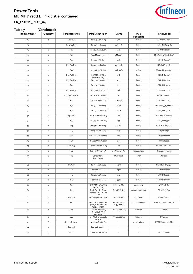
ER_201612_PL16_04 1.9 Bill of Materials
Bill of Material is shown in Table 7. Table 7 Bill of Materials
Item Number Quantity Part Reference Part Description Value PCB Footprint
IMPORTANT NOTICE The information contained in this application note is given as a hint for the implementation of the product only and shall in no event be regarded as a description or warranty of a certain functionality, condition or quality of the product. Before implementation of the product, the recipient of this application note must verify any function and other technical information given herein in the real application. Infineon Technologies hereby disclaims any and all warranties and liabilities of any kind (including without limitation warranties of non-infringement of intellectual property rights of any third party) with respect to any and all information given in this application note. The data contained in this document is exclusively intended for technically trained staff. It is the responsibility of customer’s technical departments to evaluate the suitability of the product for the intended application and the completeness of the product information given in this document with respect to such application.
For further information on the product, technology, delivery terms and conditions and prices please contact your nearest Infineon Technologies office (www.infineon.com).
WARNINGS Due to technical requirements products may contain dangerous substances. For information on the types in question please contact your nearest Infineon Technologies office. Except as otherwise explicitly approved by Infineon Technologies in a written document signed by authorized representatives of Infineon Technologies, Infineon Technologies’ products may not be used in any applications where a failure of the product or any consequences of the use thereof can reasonably be expected to result in personal injury.