WPRC 2004 Page 1 Pre-insertion Resistors in High Voltage Capacitor Bank Switching Michael Beanland, P.E., TriAxis Engineering, Corvallis, OR Thomas Speas, Southern States LLC, Hampton, GA Joe Rostron, P.E., Southern States LLC, Hampton, GA Prepared for Western Protective Relay Conference October 19-21, 2004 Spokane, WA Abstract: The switching of high-voltage capacitor banks for reactive-power or voltage support can produce significant transients. It is well understood that reactors, pre-insertion resistors, pre-insertion inductors, and synchronous switching can mitigate the transients. Circuit inductance can limit peak currents but resistance damps the oscillations most effectively. Computer simulations of transient inrush for single and back-to-back capacitor banks indicate that pre-insertion resistors can significantly reduce transients. The ability to incorporate another circuit parameter, the pre-insertion resistor, provides opportunities for improved high-voltage capacitor bank design. This paper presents an overview of capacitor switching options and the results of computer simulations for a “typical” application showing the expected transient currents in single-bank and back-to-back switching, as well as the effect of various reactor and pre-insertion resistor combinations. Results of the simulations are summarized in a table and provide the reader with a simple overview of the results of using pre-insertion resistors in capacitor switching applications. Capacitor Switching Transients Capacitor switching transients are created by the effective short circuit provided by a discharged capacitor during energization. This short circuit creates high inrush currents and the subsequent voltage dips on the source. The high inrush currents also stress switching equipment, fuses, and the capacitor units. When more than one capacitor bank exists on a common bus, the energized capacitor bank provides an extremely low source-impedance for the second switching capacitor bank leading to extremely high transient currents in both banks. In grounded wye banks, more common at higher voltages, these high transient currents can raise ground grid potentials and may damage anything tied to the same ground mat. The engineer’s goal is to control, limit and direct transient currents so that adverse effects on the source system, the capacitors, their switching devices, and associated equipment are limited to acceptable values. Since every switching event has the potential for very high currents, limiting transients also prolongs equipment life. It is hoped that a workable compromise between competing values can be achieved. When switching transients are limited in grounded banks, the required mitigation for these transients on ground grid design, control cable grounding and routing, and transient over- voltage protection can be simplified. In addition to the local effects of current and voltage transients during capacitor switching, the remote effects of “voltage magnification” at lower voltage capacitors can be an issue. Several excellent papers on this subject are available. IEEE Classic Estimates ANSI/IEEE C37.012-1979 IEEE Application Guide for Capacitance Current Switching for AC High-Voltage Circuit Breakers provides an accepted analytic approach for computation and estimation of the transient currents expected during capacitor switching. However, the complexities of modern equipment including pre-insertion inductors, pre-insertion resistors, full-time inductors, resistance of current limiting fuses are not considered in the basic IEEE methods. As such, it is an excellent guide and first-order approximation to the expected system performance. These equations are: Beanland/Speas October 20th, 2004
Transcript
WPRC 2004 Page 1
Pre-insertion Resistors in High Voltage Capacitor Bank Switching
Michael Beanland, P.E., TriAxis Engineering, Corvallis, OR Thomas Speas, Southern States LLC, Hampton, GA
Joe Rostron, P.E., Southern States LLC, Hampton, GA
Prepared for Western Protective Relay Conference October 19-21, 2004
Spokane, WA Abstract: The switching of high-voltage capacitor banks for reactive-power or voltage support can produce significant transients. It is well understood that reactors, pre-insertion resistors, pre-insertion inductors, and synchronous switching can mitigate the transients. Circuit inductance can limit peak currents but resistance damps the oscillations most effectively. Computer simulations of transient inrush for single and back-to-back capacitor banks indicate that pre-insertion resistors can significantly reduce transients. The ability to incorporate another circuit parameter, the pre-insertion resistor, provides opportunities for improved high-voltage capacitor bank design. This paper presents an overview of capacitor switching options and the results of computer simulations for a “typical” application showing the expected transient currents in single-bank and back-to-back switching, as well as the effect of various reactor and pre-insertion resistor combinations. Results of the simulations are summarized in a table and provide the reader with a simple overview of the results of using pre-insertion resistors in capacitor switching applications. Capacitor Switching Transients Capacitor switching transients are created by the effective short circuit provided by a discharged capacitor during energization. This short circuit creates high inrush currents and the subsequent voltage dips on the source. The high inrush currents also stress switching equipment, fuses, and the capacitor units. When more than one capacitor bank exists on a common bus, the energized capacitor bank provides an extremely low source-impedance for the second switching capacitor bank leading to extremely high transient currents in both banks. In grounded wye banks, more common at higher
voltages, these high transient currents can raise ground grid potentials and may damage anything tied to the same ground mat. The engineer’s goal is to control, limit and direct transient currents so that adverse effects on the source system, the capacitors, their switching devices, and associated equipment are limited to acceptable values. Since every switching event has the potential for very high currents, limiting transients also prolongs equipment life. It is hoped that a workable compromise between competing values can be achieved. When switching transients are limited in grounded banks, the required mitigation for these transients on ground grid design, control cable grounding and routing, and transient over-voltage protection can be simplified. In addition to the local effects of current and voltage transients during capacitor switching, the remote effects of “voltage magnification” at lower voltage capacitors can be an issue. Several excellent papers on this subject are available. IEEE Classic Estimates ANSI/IEEE C37.012-1979 IEEE Application Guide for Capacitance Current Switching for AC High-Voltage Circuit Breakers provides an accepted analytic approach for computation and estimation of the transient currents expected during capacitor switching. However, the complexities of modern equipment including pre-insertion inductors, pre-insertion resistors, full-time inductors, resistance of current limiting fuses are not considered in the basic IEEE methods. As such, it is an excellent guide and first-order approximation to the expected system performance. These equations are:
Beanland/Speas October 20th, 2004
WPRC 2004 Page 2
Single Bank Switching I max peak = Sqrt( 2 * Isc * Ic) Freq (Hz) = 60 * Sqrt ( Isc / Ic) Back-to-Back Switching I max peak = 1750 * Sqrt ( Vll * Ic1 * Ic2 / (Leq
current in Amperes Ic = RMS current in capacitor bank in
Amperes Vll = Line-to-line voltage in kilo-Volts Fs = 60 Hz Leq = Equivalent per-phase inductance between
capacitor banks in micro-Henrys Computer Simulations To enhance our understanding of capacitor switching transients, modern computer simulations are excellent tools. Power engineers have long used load flow and short circuit modeling software. More sophisticated area control problems make use of system stability software. However, it has been electronic engineers who have taken advantage of simulation programs such as EMTP, PSCAD, PSpice. Such simulation programs allow the engineer to create a model of the electrical system and the control system, integrate the two and observe the effects of changes in system design and control. The Bonneville Power Administration is a supporter and proponent of ATP, a public-domain version of EMTP. Such models require the user to build the model symbolically, using text or iconic symbols. PSpice is widely available, however, it requires the development of text files and has a relatively steep learning curve. The authors have used CASPOC for similar simulations. CASPOC, by Simulation Research, Netherlands, was designed for the power electronics industry to allow engineers to “build” a power system from resistors, capacitors, switches, etc. The engineer then builds, using logic blocks, the control system. Outputs from the control system can be used to control the electric circuit. CASPOC is
iconic rather than text oriented, provides feedback during the simulation, and has a quick learning curve (Valuable for us aging engineers.) CASPOC was used to develop the simulations and analyses presented in this paper. Base System To keep the system modeling for this paper within a reasonable set of parameters, a standard or “typical” capacitor bank was selected for modeling. The principles apply to any capacitor bank. Given the ease of use of the software, there is little reason not to create a specific model for each and every capacitor bank being designed or studied. For this paper we selected the following: 20,000 kVAr 3-phase (100A Ic) 115kVl-l Grounded wye 25,000A available fault duty (Isc) (500MVA) One or two identical banks Assume 20 micro-Henrys bus reactance to each bank For this system, the IEEE calculations give: Single Bank Switching I max peak = Sqrt(2 * Isc * Ic)Sqrt(2 * 25000 *
Transient Control Options For each system, we present typical transient summaries. Our focus is on worse case switching transients since these provide the proof of the design. For each case, we show the transients for switching of the first capacitor bank and the results for the switching of the second bank after the first is already energized. Each bank is independently controlled. Details of the peak current, ringing frequency, and peak voltage are provided for each portion of the switching event.
Using this “typical” capacitor bank, switching transients were examined using CASPOC. Five system configurations were studied. No Transient Limiting Full-time Inductor Pre-insertion Inductor (Standard & Enhanced) Zero-Crossing Breaker with 1ms Error Pre-insertion Resistor (Standard & Enhanced) The general diagram for the CASPOC model is shown below. The various models were created by varying component parameters and switch timings.
L1 S4
20uH S3RSOURCE LSOURCE S2 R3 L4
400u Ohm 7mH 80 Ohm 1uH S1 L2 R1 L3 SCOPE2 SCOPE1
20uH 80 Ohm 1uH
sin(0,93900,60,0,0)+
SCOPE4V1R2 20uOhm R4 20uOhm -
C1 4uF
SWITCH
i
SWITCH
i
SWITCH
iTIME1 S1 S2
C2 4uF
GROUND
SWITCHTIMES3 S4
i
In this model diagram, inductors, capacitors, and resistors are clearly shown. Oscilloscope blocks are attached to the circuit to monitor voltages and currents. Switches are shown in the circuit and their associated control blocks shown below the schematic. Each switch block has its closing time programmed as a parameter for that block.
Beanland/Speas October 20th, 2004
WPRC 2004 Page 4
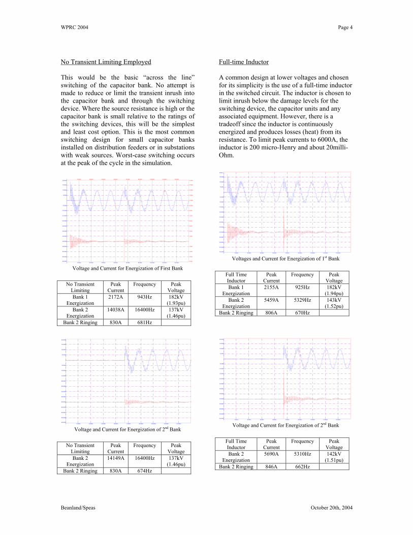
No Transient Limiting Employed Full-time Inductor This would be the basic “across the line” switching of the capacitor bank. No attempt is made to reduce or limit the transient inrush into the capacitor bank and through the switching device. Where the source resistance is high or the capacitor bank is small relative to the ratings of the switching devices, this will be the simplest and least cost option. This is the most common switching design for small capacitor banks installed on distribution feeders or in substations with weak sources. Worst-case switching occurs at the peak of the cycle in the simulation.
A common design at lower voltages and chosen for its simplicity is the use of a full-time inductor in the switched circuit. The inductor is chosen to limit inrush below the damage levels for the switching device, the capacitor units and any associated equipment. However, there is a tradeoff since the inductor is continuously energized and produces losses (heat) from its resistance. To limit peak currents to 6000A, the inductor is 200 micro-Henry and about 20milli-Ohm.
0 15.000m 30.000m 45.000m 60.000m 75.000m 90.000m 105.000m 120.000m 135.000m Voltage and Current for Energization of 2nd Bank Voltage and Current for Energization of 2nd Bank Full Time
Inductor Peak
Current Frequency Peak
Voltage Bank 2
Energization 5690A 5310Hz 142kV
(1.51pu) Bank 2 Ringing 846A 662Hz
No Transient Limiting
Peak Current
Frequency Peak Voltage
Bank 2 Energization
14149A 16400Hz 137kV (1.46pu)
Bank 2 Ringing 830A 674Hz
Beanland/Speas October 20th, 2004
WPRC 2004 Page 5
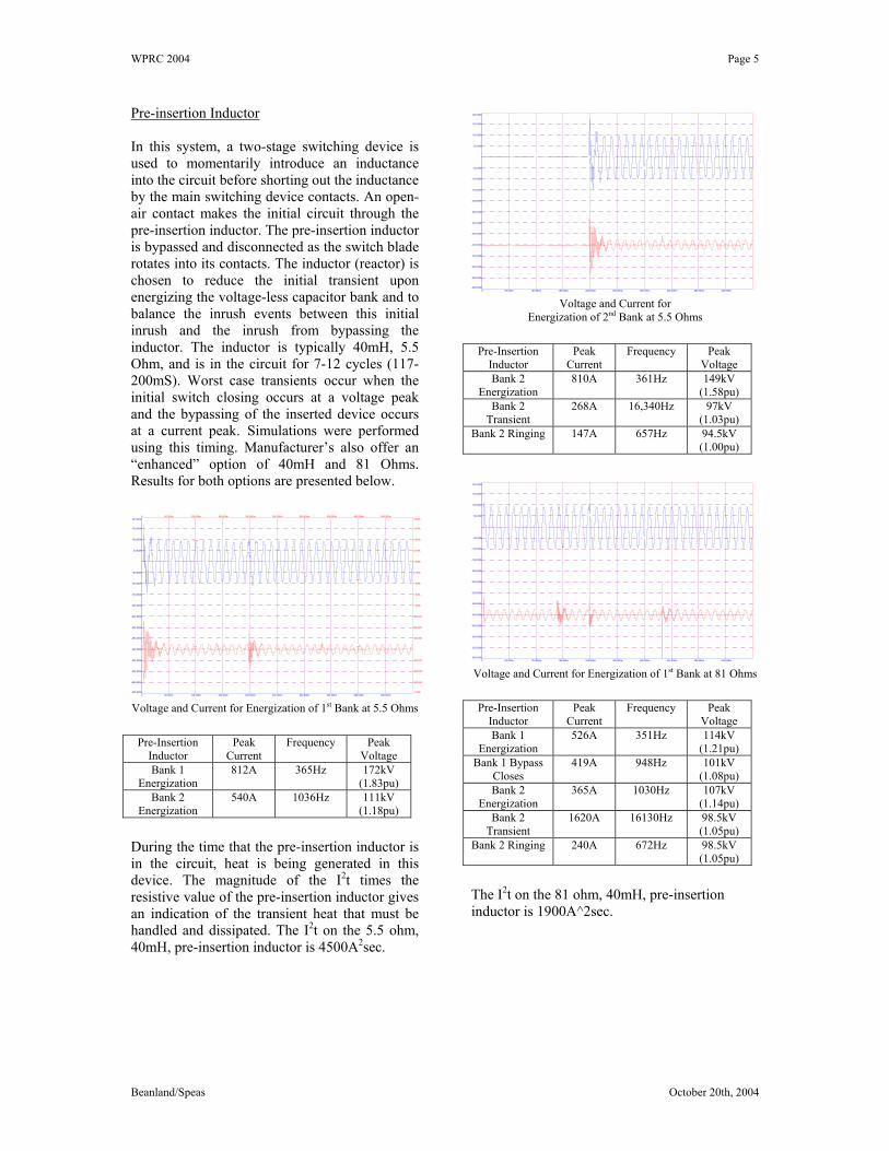
Pre-insertion Inductor In this system, a two-stage switching device is used to momentarily introduce an inductance into the circuit before shorting out the inductance by the main switching device contacts. An open-air contact makes the initial circuit through the pre-insertion inductor. The pre-insertion inductor is bypassed and disconnected as the switch blade rotates into its contacts. The inductor (reactor) is chosen to reduce the initial transient upon energizing the voltage-less capacitor bank and to balance the inrush events between this initial inrush and the inrush from bypassing the inductor. The inductor is typically 40mH, 5.5 Ohm, and is in the circuit for 7-12 cycles (117-200mS). Worst case transients occur when the initial switch closing occurs at a voltage peak and the bypassing of the inserted device occurs at a current peak. Simulations were performed using this timing. Manufacturer’s also offer an “enhanced” option of 40mH and 81 Ohms. Results for both options are presented below.
0 60.000m 120.000m 180.000m 240.000m 300.000m 360.000m 420.000m 480.000m 540.000m Voltage and Current for
Energization of 2nd Bank at 5.5 Ohms
Pre-Insertion Inductor
Peak Current
Frequency Peak Voltage
Bank 2 Energization
810A 361Hz 149kV (1.58pu)
Bank 2 Transient
268A 16,340Hz 97kV (1.03pu)
Bank 2 Ringing 147A 657Hz 94.5kV (1.00pu)
50.000k
100.000k
150.000k
-50.000k
-100.000k
-150.000k
-200.000k
-250.000k
-300.000k
-350.000k
-400.000k
-450.000k
-500.000k
-550.000k
-600.000k
200.000k
0 60.000m 120.000m 180.000m 240.000m 300.000m 360.000m 420.000m 480.000m 540.000m Voltage and Current for Energization of 1st Bank at 81 Ohms
Voltage and Current for Energization of 1st Bank at 5.5 Ohms Pre-Insertion
Inductor Peak
Current Frequency Peak
Voltage Bank 1
Energization 526A 351Hz 114kV
(1.21pu) Bank 1 Bypass
Closes 419A 948Hz 101kV
(1.08pu) Bank 2
Energization 365A 1030Hz 107kV
(1.14pu) Bank 2
Transient 1620A 16130Hz 98.5kV
(1.05pu) Bank 2 Ringing 240A 672Hz 98.5kV
(1.05pu)
Pre-Insertion
Inductor Peak
Current Frequency Peak
Voltage Bank 1
Energization 812A 365Hz 172kV
(1.83pu) Bank 2
Energization 540A 1036Hz 111kV
(1.18pu)
During the time that the pre-insertion inductor is in the circuit, heat is being generated in this device. The magnitude of the I2t times the resistive value of the pre-insertion inductor gives an indication of the transient heat that must be handled and dissipated. The I2t on the 5.5 ohm, 40mH, pre-insertion inductor is 4500A2sec.
The I2t on the 81 ohm, 40mH, pre-insertion inductor is 1900A^2sec.
0 15.000m 30.000m 45.000m 60.000m 75.000m 90.000m 105.000m 120.000m 135.000m Voltage and Current for Energization of 1st Bank Voltage and Current for Energization of 2nd Bank at 81 Ohms
Zero-crossing Breaker Modern control systems attempt to exploit the ability to precisely and repetitively control with precision the instant at which the switching contacts come together. Under ideal circumstances, if the poles close at the point of zero-voltage, there will be no current transients created. This requires precise timing and control of the three individual poles. Any drift in the control must be compensated for or else the system reverts toward the first case above. Simulations for 1mS closing error are performed. This error is chosen for simulation purposes only and is not meant to be indicative of the actual zero-crossing performance of any specific breaker or installation.
Voltage and Current for Energization of 2nd Bank
Zero-crossing Breaker
Peak Current
Frequency Peak Voltage
Bank 2 Energization
5228A 16,667Hz 108kV (1.15pu)
Bank 2 Ringing 420A 670Hz
Beanland/Speas October 20th, 2004
WPRC 2004 Page 7
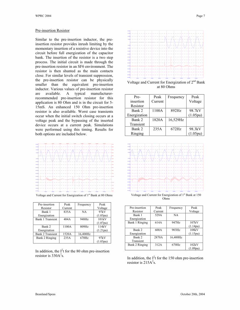
Pre-insertion Resistor Similar to the pre-insertion inductor, the pre-insertion resistor provides inrush limiting by the momentary insertion of a resistive device into the circuit before full energization of the capacitor bank. The insertion of the resistor is a two step process. The initial circuit is made through the pre-insertion resistor in an SF6 environment. The resistor is then shunted as the main contacts close. For similar levels of transient suppression, the pre-insertion resistor can be physically smaller than the equivalent pre-insertion inductor. Various values of pre-insertion resistor are available. A typical manufacturer-recommended pre-insertion resistor for this application is 80 Ohm and is in the circuit for 5-15mS. An enhanced 150 Ohm pre-insertion resistor is also available. Worst case transients occur when the initial switch closing occurs at a voltage peak and the bypassing of the inserted device occurs at a current peak. Simulations were performed using this timing. Results for both options are included below.
In order to verify the basic system modeling approach, actual field test results for operation of a pre-insertion resistor switch were obtained courtesy of a U. S. investor owned utility. The actual transient records (oscillograph results attached) were compared to a simulation model (results attached). The results agree favorably in that peak transient currents are of the same magnitude and ringing frequencies are similar. The actual results show lower transients magnitudes and less ringing upon pre-insertion resistor bypass. These can be explained by the lack of detailed component data used in to build the model. Higher actual component resistances than those used in the model will lead to reduced transients. Substation load will cause some additional damping of transients. Also, current transformer hysteresis may add to current measurement error at the 4500Hz ringing frequencies.
Voltage and Current for Energization of 2nd Bank at 150 Ohms
Pre-insertion
Resistor Peak
Current Frequency Peak
Voltage Bank 2
Energization 600A 860Hz
Bank 2 Transient
3170A 16,529Hz
Bank 2 Ringing 312A 671Hz 102kV (1.09pu)
Generally, the model provides good agreement with the recorded data.
Summary The following table summarizes the most significant data in the above results:
Conclusions The conclusions we would like to take from this work are:
1) IEEE guidelines for calculation of capacitor switching transients are good first estimates for transients with no limiting applied.
2) The engineer has several options for limiting transient events during capacitor switching. a. The full time inductor, pre-insertion inductor, zero-crossing breaker, and pre-insertion
resistor successfully mitigate current transients.
b. Devices with resistance provide the added advantage of reducing voltage transients. Proper selection of the resistance value can significantly reduce voltage transients.
c. Zero-crossing switching shows good transient mitigation but transients will increase if timing calibration drifts.
d. The transients from connection of the pre-insertion device and those from bypassing the pre-insertion device need to be considered.
3) Transient modeling, by computer simulation software, has produced results that are consistent with actual field testing.
4) Modern computer simulation software can provide the engineer with a better understanding of the transient events during capacitor switching.
5) Because every capacitor bank and electric system is different, the designer must analyze the situation and tailor the switching device accordingly. Manufacturer’s offer variations to aid the designer in this customization.
References “Innovations for Protection and Control of High Voltage Capacitor Banks on the Virginia Power System,” Jeffery F. Peggs, Phillip W. Powell, Thomas E. Grebe, 1994 IEEE/PES Transmission and Distribution Conference and Exposition “Impact of Utility Switched Capacitors on Customer Systems – Magnification at Low Voltage Capacitors,” M. F. McGranaghan, R. M. Zavadil, G. Hensley, T. Singh, M. Samotyj, 1991 IEEE PES Transmission and Distribution Exposition “Synchronous MV Circuit-Breaker with Magnetic Drive and Electronic Control,” Carlo Cereda, Carlo Gemme, Christian Rueber, ABB Review 6/1999
“S&C Circuit Switchers – Mark V,” Data Bulletin 711-95 “Capacitor switching needs a switch, not a circuit breaker,” Electrical World, April 1996 “The SyncCap Power Quality Switch: Minimizing Switching Transients on Power Systems During Capacitor Switching,” Frank DeCesaro, John Baranoski, Michael Dunk, Dwayne Tector, Cooper Power Systems Southern States CapSwitcher Product Specification Guide, Publication No. PSG-807-031904
Beanland/Speas October 20th, 2004
WPRC 2004 Page 10
Beanland/Speas October 20th, 2004
Oscillograph from Installation at U. S. Utility
For CapSwitcher® Capacitor Switch with Pre-Insertion Resistors
WPRC 2004 Page 11
Beanland/Speas October 20th, 2004
IaIaIaIaIbIb
IbIbIcIcIcIc
SCOPE1
VOLTAGE
V(Vc)
VOLTAGE
V(Vb)
VOLTAGE
V(Va)
Va
Va
VaVa
Vb
VbVb
Vb
VcVc
Vc
Vc
SCOPE3
VOLTAGE
V(Vcn)
VOLTAGE
V(Vcc)
VOLTAGE
V(Vcb)
VOLTAGE
V(Vca)
Va
Va
VaVaVbVb
Vb
Vb
Vc
Vc
Vc
VcVNVNVNVN
SCOPE2R1A
17 Ohm
R2A 10m
C3A 17.158uF
C3B 17.158uF
C3C 17.158uF
R2B 10m
R2C 10m
L2B 20uH
L2C 20uH R1C
17 Ohm
R1B
17 Ohm
B3+
-
LXFMRC
100uH
LXFMRB
100uH
B2+
-
LXFMRA
100uH
B1+
-
SWITCH
i
SWITCH
i
SWITCH
i
SIGNAL
time
DC
AC
F
Phase
d
RXFMRA
2m
SIGNAL
time
DC
AC
F
Phase
d
RXFMRB
2m
RXFMRC
2mSIGNAL
time
DC
AC
F
Phase
d
SWITCH
i
SWITCH
i
SWITCH
i
TIME
L2A 20uH
SC1
SC2
SB1
SB2
SA1
SA2
VOLTAGEC
VOLTAGEB
VOLTAGEA
VOLTCN
VOLTCC
VOLTCB
VOLTCA
VCA
VCB
VCC
VCN
TIME1 SW1A SW1B SW1C
2.0944
60
41858
SIGNALC
GROUND
VC
VB
SIGNALB
41858
60
4.1888
VA
SIGNALA
41858
60
0
SW2A SW2B SW2C
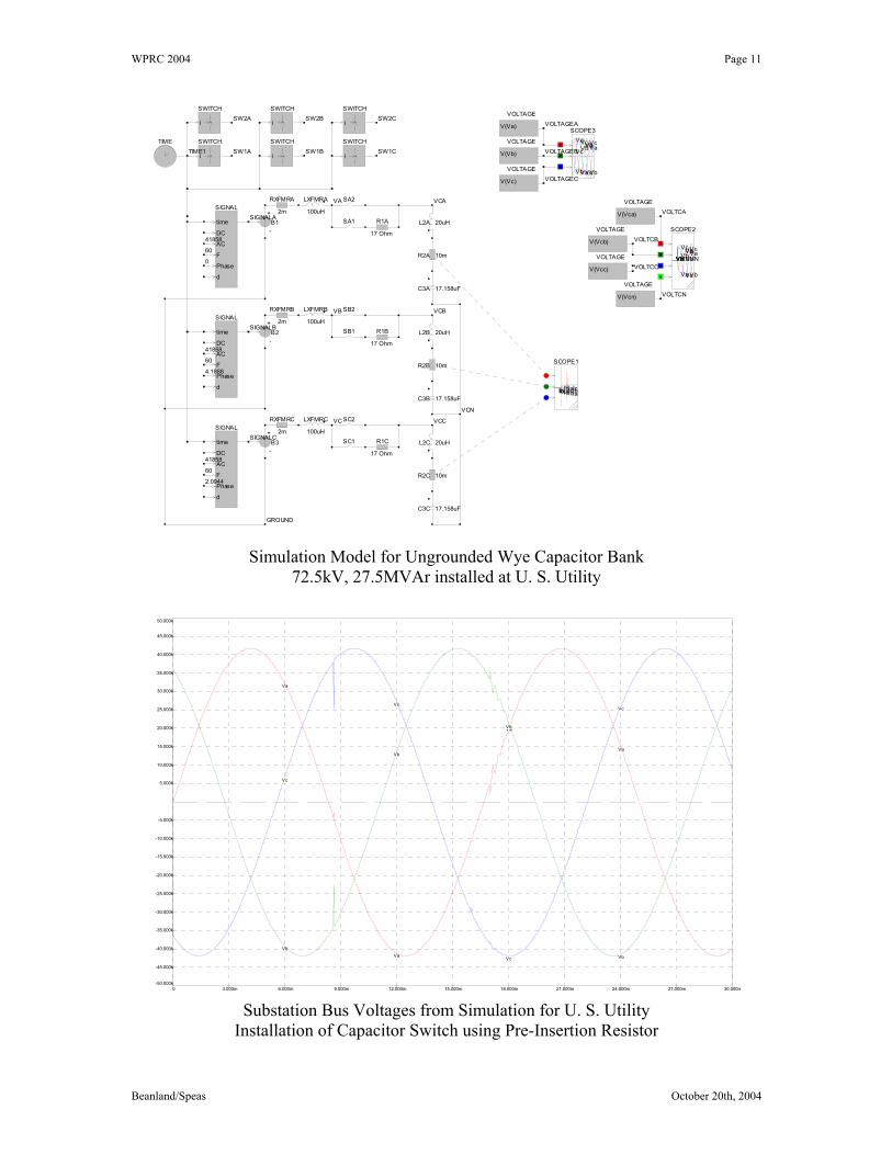
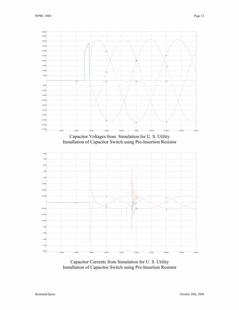
Simulation Model for Ungrounded Wye Capacitor Bank