A bst r ad Printed Circuit Board Inspection Robert Thibadeau The Robotics Institute Carnegie-Mellon University 25 November 1981 This paper provides a general overview of immediate and long-term aims of the printed circuit board inspection project of The Robotics Institute. Its purpose is to highlight some of the significant issues specific to printed circuit board inspection and to provide a discussion of our basic thesis that machine inspection should be coupled with machine diagnosis of the causes of observed printed circuit board defects . Copyright @ 1981 Robert Thibadeau,CMU Robotics Inst. This research was supported by The Robotics Institute, Carnegie-Mellon University, Pittsburgh, PA 1521 3. Other members of the printed circuit board inspection project are Mark Friedman, Raj Reddy, and Robert Berger.
Transcript
A bst r a d
Printed Circuit Board Inspection
Robert Thibadeau The Robotics Institute
Carnegie-Mellon University
25 November 1981
This paper provides a general overview of immediate and long-term aims of the printed circuit board inspection project of The Robotics Institute. Its purpose is to highlight some of the significant issues specific to printed circuit board inspection and to provide a discussion of our basic thesis that machine inspection should be coupled with machine diagnosis of the causes of observed printed circuit board defects .
Copyright @ 1981 Robert Thibadeau,CMU Robotics Inst.
This research was supported by The Robotics Institute, Carnegie-Mellon University, Pittsburgh, PA 1521 3.
Other members of the printed circuit board inspection project are Mark Friedman, Raj Reddy, and Robert Berger.
i
Table of Contents 1. Introduction 2. Methods of Inspection 3. A Closer Look At Printed Circuit Boards 4. Overview of the Diagnostics Station 5. Some Software Assessments of Fast Flagging Methods
6. Some Aspects of Pattern Recognition 7. Concluding Remarks
1 2 3
12 16 16 17 18 19 21 21 23 24 24 26
ii
List of Figures Figure 3- 1 : A magnified image of a good circuit. Figure 3-2: Example of Spurious Copper. Figure 3-3: Example of a Short. Figure 3-4: Example of a Nick. Figure 3-5: Example of a Pin Hole. Figure 3-6: Example of a Break. Figure 3-7: Example of a Scratch. Figure 4-1 : The diagnostics facility. Figure 5-1: An artists rendition of the difference between a smooth edge and one
showing quantization noise. To see real quantization noise look carefully at the copper edges in Figures 3-1 through 3-7.
Figure 5-2: Run Length Histogram. Figure 5-3: Two objects so highly magnified that their picture elements stand out as
squares with superimposed arrows to indicate the edge vectors encoded by the edge tracking algorithm.
... 111
List of Tables Table 6- 1 : Fault Analysis
4 6 7 8 9
10 11 13 17
22 24
26
1
1. Introduction Printed circuit boards are rigid or semi-rigid boards on which geometrical patterns are printed in
copper or some other conductive material. They function to replace the wiring and perhaps some of
the electrical circuit components’ in everything from toasters to fighter planes. Printing a wire can be
less expensive than fitting a real one and soldering it. The sorts of printed circuit boards which are of
immediate interest to us are those that become, in later stages of fabrication, inner layers of multilayer
laminated boards. Multilayer boards involve many strata of wiring in highly complex circuits. If an
inner layer board has one chance in ten of a defect, and ten inner layers form a single laminated
board, nearly two-thirds of the finished boards will have to be thrown away due to defective wiring.
This provides strong motivation for inspecting inner layers, in one way or another, before lamination.
The automated inspection of printed circuit boards (PCBs) serves a purpose which is traditional in
computer technology. The purpose is to relieve human inspectors of the tedious and inefficient task
of looking for those defects in PCBs which could lead to electrical failure. For example, circuit breaks
have rather obvious implications for electrical failure, and human inspectors often miss those defects.
It is simply hard to visually inspect hundreds of thousands of printed wires, each a few thousandths of
an inch across, for many hours a day and not make mistakes. Such mistakes, while perfectly
understandable, are also costly. The time is anticipated when the print on the boards will be so fine
that human inspectors must use microscopes rather than the magnifying glasses now in use. With
the rapid- movement limitations of microscopic viewing, the inefficiency of human inspection will be
intolerable. Automated, computer based, inspection relieves this problem by providing a machine
solution. Obviously, there are managerial, employment, and wide-ranging economic implications of
such technology which must be considered along with the technology itself. While these topics are
important and worthwhile, this paper focuses just on the engineering attributes and potential of
automated printed circuit board inspection.
’Nowadays people distinguish between printed circuit boards or PCBs and printed wiring boards or PWBs to keep clear which boards contain electrical circuit elements (e.g., resistors) and which contain only wiring. The generic term is printed circuit board or PCB. It is this usage which is addressed in the present paper.
2
Our first goal is to produce automated inspection stations. Industry needs them for practical
reasons, and we need them as tools to stimulate research in other areas. For example, we are
currently developing an inventory of .techniques for computer inspection of a wide variety of other
products (e.g., common tiles, flat objects uniformly painted, integrated circuit artwork masters). But
the thesis of this paper does not directly concern these important aspects of our research. The thesis
is that automated inspection stations have potential for more than simple circuit defect detection.
There are two major points. First, an automated inspection station, designed using computer
technology, can keep records of its activity in a form which managers and engineers can evaluate.
Such records are often not available from human inspectors. Second, in the present age of
information, an inspection station can be transformed to a diagnostics station. The station can make
inferences about the causes of the defects which it notices, and pass this digested information
forward. Such a station can become an integral part of eliminating the causes of defects in PCBs.
2. Methods of Inspection Automated inspection is a familiar concept nowadays, but some types of manufacture are more
conducive to automated inspection than others. One would think a 'bed of nails,' testing every
electrical connection, would be the ideal PCB inspection technique. It some applications it is, but, in
many, the boards are far too frail to suffer much contact with other hard surfaces. The 'bed of nails'
can create more defects than it finds. Such circumstances require non-contact techniques for
inspection.
One candidate for non-contact inspection is the comparator technique. Here either a "perfect"
board or stored computer "perfect board image" is compared to each board to be judged. If the
sample does not match the perfect board, it is classified as a faulty board. We know that a memory
comparator technique has met with particular success on paper money in the U.S. Mint2. But a
drawback of this technique is the time it requires to construct the stored computer images (on the
order of months). Printed circuit boards, unlike dollar bills, are typically manufactured in small
batches, and this makes storing new perfect board images uneconomical. The comparator
techniques which do not require storing the perfect board image simply do not work very well. Good
boards vary enough among themselves to make such optical comparison risky. Furthermore,
comparator techniques, in general, have high monetary cost because of the precision required of the
imaging equipment. Complete X-Y stability, and thus a heavy, high-precision, device, is required. It is
'Personal Communication with Officers of the Mint. The Mint uses a one-of-a-kind product by Perkins-Elmer Corporation.
3
no surprise to find comparator approaches non-competitive for automated PCB inspection.
Another approach mixes together many hardware sensors each with a special function. For
example there may be a number of different optical sensors mixed together to give one effective
inspection. This has been tried (e.g., [Bentley 79]), and certainly has the merit of well-adapted
hardware, but a rube-goldberg style device is invited with all the attendant problems to be expected of
such hardware specialization. Specialized hardware is also unlikely to prove adaptable to changes in
PCB design and fabrication. Finally, there is a problem of what process control function that
hardware is capable of performing.
The present approach is a rule-based or computational solution to inspection. It places emphasis
not only on detecting defects in PCBs, but also extends in labeling and describing the defects in a
process control sense. We believe neither a comparator approach, nor a hardware-constrained
approach to vision, is likely to extend naturally in this direction. Much of the work of inspection is
performed by software. The hardware (including cameras, optics, and electronic processing
components) is general to all planar imaging. Only the software and mechanics of board handling is
specialized to the inspection purpose at hand. This method has much potential for success although
extensibility is not guaranteed, and sometimes it is actually prohibited in an inspection method (cf.,
[Sterling 791). With care, however, rapid and effective rule-based inspections can be used to catch
defects, identify their nature, and describe their causes as well. To understand how this might be
possible, we need to consider the PCBs, and something about how computer vision of PCBs works.
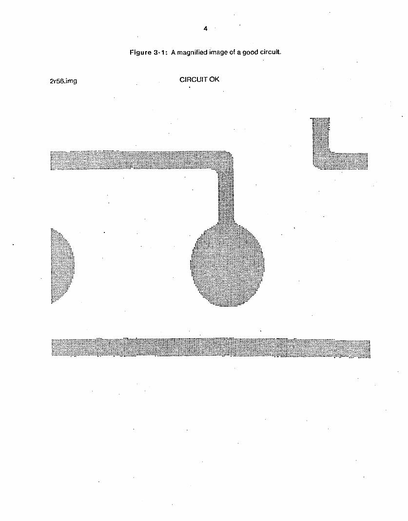
3. A Closer Look At Printed Circuit Boards PCBs are fabricated in enormous variety. The prototype is the fiberglass board on which is printed
a design in copper. The design is typically composed of lines in a maze-like pattern with the
constraint that all lines end in round pads. A magnified view of lines and pads is shown in the image
in Figure 3-1. Many variants on the illustrated geometry are possible, including the presence of drill
holes through the centers of the pads, a selection of substrate materials, unetched copper-clad
boards, electrical-ground boards with wholly different geometries, and even soldered boards after the
electronics are attached. The image in Figure 3-1 is most common for boards in our possession. The
line widths on a board can range from .01 to .02 inch and the pad diameters from .06 to -10 inch.
It may be surprising that for many years (say, 20) students of computer vision have been interested
in the computer interpretation of PCBs (see [Pavlidis 771). One reason, of course, is that PCBs were
available to these people. But the interest in PCBs has persevered because the computer vision
Figure 3- 1 : A magnified image of a good circuit.
2r56.img CIRCUIT OK
i 2 . .- .... ..._.....
5
problem is both useful and two-dimensional. Students of computer vision naturally first gravitated
towards interpreting objects which are two-dimensional. They are simpler than three-dimensional
objects. Printed circuit boards, and, indeed, printed matter in general, are two-dimensional objects of
practical importance.
Computer processing of PCBs is no longer widely researched in basic science perhaps because
the inspection goal has not been emphasized. As a matter of pattern recognition of good boards, new
ideas using standard computer technology have pretty much been exhausted. But the matter goes
further than simple pattern recognition, and that is where things get interesting. The purpose in
having a computer inspect a printed circuit board is not in having it recognize good patterns, though
that is certainly necessary. The purpose is in having the computer comprehend bad patterns. A
defect in a printed circuit board is, by definition, an unpredictable pattern. It is this unpredictability
that makes imaging and interpreting defects an interesting and still vital research goal. It also makes
the research something more of a problem of artificial intelligence than of simple pattern recognition.
What is important to our thesis is that the pattern recognition not only produce interpretations of lines,
pads, and other normal copper configurations, but also interpretations of defective areas. This point
is not mysterious, though it may be subtle. Simply stated, a piece of the copper (or substrate) is
defective. Finding that defective piece and labeling it is important and is interesting.
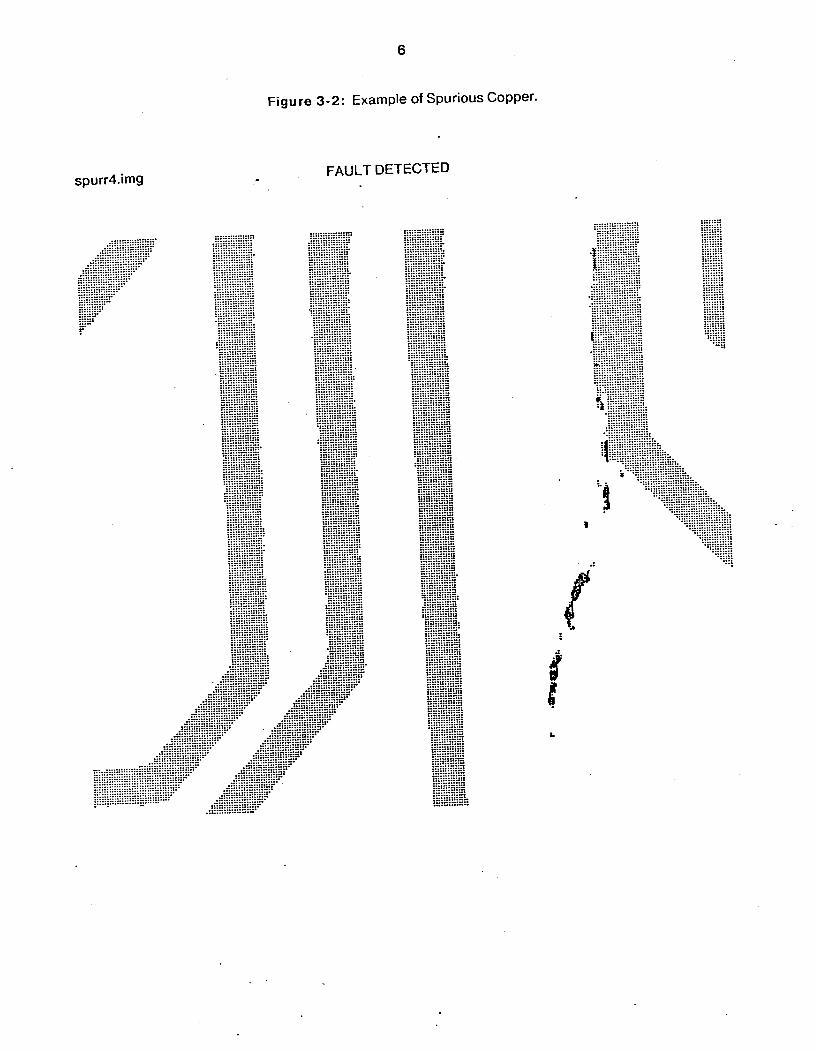
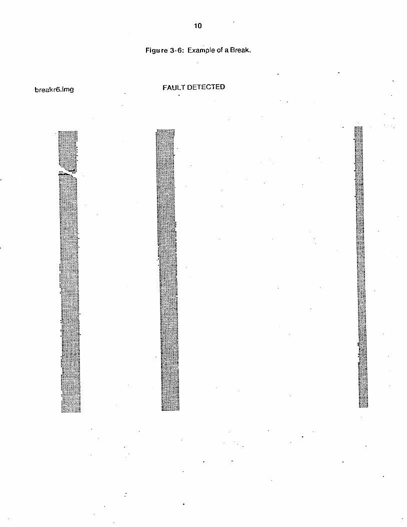
For concreteness, Figures 3-2 through 3-7 contains a series of images of defects of various types
and varying degrees of severity. These images are all real camera images, but, like Figure 3-1, they
have been artificially 'half-toned' owing to the limitations of our printing medium. Defects have been
blackened under computer control using a technique to be described in a later section of this paper.
Note this particular technique characteristically blackens only copper areas in proximity to defects -- not necessarily the defects themselves. This should be considered a major property of the defect
detection technique. The images, though containing blackened regions, are nevertheless binary
images in that only two types of picture element occur in the image per se, either white space or dark
(copper) space. The picture elements, also termed pixels, correspond to the minimum uniform
resolution which, in the present case, is approximately 2/3 mil (.0067 inch) square. Binary imaging is
not a necessary feature of two-dimensional vision; gray scale and color imaging may occasionally be
useful. Nevertheless, in initially focusing on the problem of defect identification practical
considerations go against such exotic imaging on a routine basis.
The promotion of binary images may call to question the supposition that printed circuit boards are
two-dimensional objects. Printed circuit boards are not really 'printed', but copper is etched off a
smoothly plated board to form the 'printed circuit.' The etching, as the name implies, leaves a three-
dimensional form even though the depth is small. Common defects are associated with under-
etching (leaving too much copper) or over-etching (leaving too little). These are clearly three-
dimensional problems. Fortunately, it appears that, in most instances, three-dimensional problems
have their two-dimensional correlates. For example, under-etching generally results in lines of too
much width and spurious copper (Figure 3-2) or shorts (Figure 3-3), and over-etching results in thin
lines, apparent nicks, scratches, holes or breaks (Figures 3-4 through 3-7). Depth of copper problems
can often be inferred even though we treat the vision problem primarily as a problem of two-
dimensional binary vision. This is the traditional answer to the question of why PCB inspection is
regarded as a binary vision problem of two-dimensions, and it continues to provide a sound working
assumption .
4. Overview of the Diagnostics Station A diagnostics station, which combines an inspection station with diagnostic capability, is a
complicated system but nowhere near approaching workable limits. Such a station is reasonably but
a part of the diagnostics potential of the factory of the future [Fox 811. PCB inspection involves only a
limited range of sensors, primarily optical and mechanical, and virtually no novel robotic manipulation
capability. PCB defect diagnosis may involve other sensors such as thermal and chemical ones
associated with the etching process. But initially we are concerned with evaluating one point in the
manufacturing process, where a total scheme would include more. We believe a single diagnostics
facility may serve as the basis for expansion, and, in fact, i f designed with extensibility in mind, can
remain an part of the productivity of the factory even through dramatic changes in PCB design and
fabrication.
A chart of the diagnostics facility is provided in Figure 4-1 in order to highlight the important parts
and their interactions. At one end providing input to fast flagging is the camera and method by
which PCBs are manipulated, imaged, and passed on. At the other end is information tailored to
managers, quality control engineers, and design engineers. The information has to meet the
criteria of (a) quality, (b) verifiability, and (c) speed. Before continuing with Figure 4-1, let us consider
these criteria in detail.
By quality we mean that the information output must be 'human engineered information'. For
example, the diagnostics station should not conclude over-etching with suggested remedies if only
enough evidence to support the possibility of over-etching exists. It can legitimately conclude,
however, with a list of all the possibilities - - perhaps requesting of the operator a specific test of its
best guess. A circuit break appearing repeatedly on all boards within a group suggests a problem
13
Diagnostics
Abst ractiin I Engine A
INSPECTION STATION
Figure 4- 1 : The diagnostics facility.
I I I # I DIAGNOSTICS STATION I
PC VISION
\ \ \ \
14
with the artwork master, if the break is regular enough. The system might then propose the artwork
master be checked before fabricating any more boards of that group. If that fails, other, less likely,
causes capable of introducing a constant defect may be hypothesized and checked (e.g., dust on the
light-plate used to transfer the board design from the artwork negative).
The information output must be verifiable -- if only to insure a basis for knowing to trust the
diagnostics station (and perhaps how not to trust it). One form of verifiability can readily be provided
to human eyes by video gray scale images of the defects. Also important is the capability of
explaining a defect. One may judge for himself the validity of such a claim on a spot basis. Finally,
the "raw numbers" must always be available. One can call up statistics on the pattern of defects
categorized by board, manufacturing path, and so forth.
The requirements of quality and verifiability are worth little, however, if the diagnostics station
cannot keep up with the rate of board fabrication. The station must do its job rapidly. Classically
computer vision is slow. We must have it fast. A board of 100 square inches of surface area,
inspected at let us say 2/3 of a mil per picture element provides some quarter of a billion picture
elements to the system. If one picture element is evaluated per millisecond the result is a horribly
slow system. It would take over sixty hours to evaluate a single board. If one picture element is
evaluated per microsecond, the inspection and diagnosis time is less than four minutes per board.
Four minutes is in fact comparable to human times, and, even so, is not unreasonable since several
copies of the same inspection station can share the load and bring this value down to meet virtually
any production schedule.
Speed is as important for research as for any industrial purpose. The reason has to do with ease in
doing experiments to develop improved methods for inspection and diagnosis. Since the system
relies primarily on software, experiments on new methods can be obtained without new hardware. If
an experiment on a new inspection method requires a thousand boards, a value of 156 twenty-four
hour days to do a single experiment is far less interesting than a value of two such days.
Experimentation, by its very nature, requires many experiments.
Understanding the need for quality, verifiability, and speed, the parts of the diagnostics facility in
Figure 4-1 are more obvious. At one level is the inspection station. This is composed of general
purpose imaging equipment and general-purpose high-speed computing eq~iprnent.~ The computing
3The system presently uses a Three Rivers Corp. PERQ for its computer. The major attractive features are low cost, speed (approximately 7 million microcycles per second), large address space (20 bits), "raster-op" hardware, and system integration already including a hard-disk, graphics display, keyboard, operating system, and PASCAL compiler.
15
equipment is programmed to perform a cursory but effective fast flagging of potential defects in the
boards. Many of the pixels (over 95%) are therefore rapidly removed from consideration and only a
fraction of the original number retained for further processing. It is possible to tune this coarse
analysis by some small number of parameters abstracted from a design data base, and it is also
possible, without much time consumption, to keep statistics on the various boards and defects
detected. This kernel constitutes a workable inspection station in itself. In fact, most current
proposals for inspection stations, most more reliant on special hardware, do not propose any further
The diagnostics station incorporates three new parts to suppliment the coarse initial board analysis
with a fine analysis of the defects. The three parts exist solely in software and are kept up to date and
altered as board design and manufacture change. They are pattern recognition, a so-called
diagnostics engine, and a causal model of the fabrication process. Pattern recognition
provides the descriptions of the images which have been flagged as showing board defects. Such
descriptions include the classification into circuit defect categories such as break, nick, short,
spurious copper, and pin hole. Furthermore they include the location of these defects in context.
The local context is relative position, orientation, and adjacency within the image, while the global
context is such things as the approximate location on the board, the board ID number, and
manufacturing path. Such descriptions constitute a major input to the diagnostics engine. The
diagnostics engine compares these descriptions and descriptions obtained from other inputs, such
as chemical sensors, to a causal model of the manufacturing process which can be maintained
separately as part of the management of the entire factory [Fox 811. The engine provides judgements
on the causes of the defects, and thereby completes the diagnosis of the defects.
The chart in Figure 4-1 shows feeding information through a graphics display terminal to affect
management, design, artwork, and manufacturing methods. A graphics terminal can provide
all the required information to human consumers, including images of defects, verbal suggestions
and conclusions. This one arrangement is preferred for its flexibility and power to meet new
demands. Eventually this will permit 'closing the loop' -- letting the diagnostic information direct
automated improvements in the manufacturing stream. By framing information in terms of the
fabrication process itself, the diagnostics facility fulfills this need without modification.
16
5. Some Software Assessments of Fast Flagging Methods A variety of fast-flagging methods have been assessed for their attributes in PCB inspection and
defect diagnosis. In this section, we evaluate several which we have developed or which have been
used with success by others. The evaluation has included first-hand experience with these
algorithms on a data base on over 1500 480 X 512 pixel images of PCBs at approximately 2/3 mil
(.0067 inch) per pixel resolution. The purpose of this discussion is not to come to some conclusion
about the most preferable method, but rather to overview a range of methods with a mind toward
having several good methods available.
The commonality which underlies all the fast-flagging techniques (in one way or another) is a
reliance on a notion of spatial frequency. The idea is that defective copper areas show up in areas of
'jaggedness' or disruption of normal geometries. These areas appear as too small to fit expected
local sizes (line widths, pad diameters, spacings between lines and pads). The need for rapidity in
fast-flagging is the reason why no one simply measures every aspect of the circuit for dimensions
which do not meet the specifications for a good circuit.
In general, all the fast-flagging techniques have the attribute of detecting defects reliably. Types of
defects that may be missed are noted. Also important is the likelihood that a technique will falsely
detect a defect when none actually exists. Although the more careful pattern analysis that follows
fast-flagging eliminates such false alarms, a high false alarm rate will significantly slow the
performance of the system as a whole. Finally, in keeping with the topic of extensibility to diagnosis,
comments are made on how each algorithm labels a defect. The important question concerns the
part of the copper and substrate the algorithm terms "defective". Interestingly, different algorithms,
detecting the same defect, label different parts of the copper or substrate defective.
5.1. Expansion-Contraction
The expansion-contraction method can discriminate high from low spatial frequency. It was first
proposed by [Ejiri 731. To be effective, this method requires two measures, one for an expansion-
contraction-compare operation and one for the opposite contraction-expansion-compare operation.
In the former case the edges of the copper image are uniformly expanded some preselected
distance, then the result of the expansion is uniformly contracted the same distance. A comparison
against the original image is then made to determine if the expansion literally enveloped small areas
which the contraction did not reopen. Those small areas are at spatial frequencies which are too high
for normal geometries on the board, and therefore suggest defects. Expansion-first is capable of
17
detecting nicks, and the like. Contraction-first is capable, similarly, of detecting protrusions.
Among the positive attributes of this technique are a straightforward hardware implementation for
high speed [Ejiri 731. In our software version, we were free to manipulate the radius of the circular
expansion and contraction windows in order to better evaluate the effectiveness of this procedure.
On the whole, the procedure performs well, but there are some limitations. Circuit breaks are missed
whenever the spacing between conductors is as large as any reasonable expansion. The maximum
initial contraction is limited by the smallest legitimate line width, and this means that certain
protrusions will go unnoticed. Finally, this technique is sensitive to the small spatial frequencies in
the quantization noise (or 'castle edging' illustrated in Figure 5-1) characteristic of all practical binary
imaging. That noise must be filtered to avoid continuous false alarms.
The area of an image labeled "defective" by this technique is either a 'blob' of substrate (in
expansion first) or a 'blob' of copper (in contraction first). For example a pin hole in a pad would
show up as a defect filling the image of the hole. The defective area, then, will tend to use as much of
the existing boundaries (copper edges) as possible in its boundaries. This may be viewed as a
positive attribute of the coarse analysis.
Figure 5- 1 : An artists rendition of the difference between a smooth edge and one showing quantization noise. To see real quantization noise look
carefully at the copper edges in Figures 3-1 through 3-7.
5.2. Table Lookup
Speed in software can often be improved by replacing computation with lookup in stored tables
(where the computation is done once and for all time). At least one PCB inspection method has been
proposed along these lines [Jarvis 801. The idea is to form a table of images from good boards. After
sufficient training, any newly acquired image which is not found in the table is flagged as containing a
potential defect. Although this technique is similar to a memory comparator technique, it differs in
that the images are not images of whole boards. The images are usually square samples of the board
images called "windows".
18
The risk with this technique is that the number of table entries can grow so large that the technique
may lose its speed advantage over direct computation. For example, a 7 X 7 pixel window providing
table entries may reference a table with as many as 2@ entries. To reduce redundancy, a 7 X 7 pixel
window may be considered only if the center pixels are on a copper edge, and the edge may be
normalized by horizontal and vertical symmetry from the fact that there are four edge types
associated with square pixel elements. Even with these simplifications, we find the table can rapidly
become too large to handle (with the speed required). [Jarvis 801 has found that his table grew
without apparent limit, and we have now extended his results from 80 256 X 256 pixel images to the
same result at 100 480 X 512 pixel images. Our table grew to more than 4000 entries and never
showed any signs of asymptotic growth. A problem is that training (entering new images) produces
many outliers that are never apt to be found in other images, and often the table lookup will signal a
defect due to quantization mismatches - - not due to any serious mismatch. Filtering out quantization
noise is potentially very costly in this type of processing unless the filtering occurs in hardware.
Locally smooth defects (e.g., smooth line breaks), which mimic good surfaces of the circuit, are apt to
go unnoticed. They would be less apt to go unnoticed if the window (currently 7x7 pixels) could be
made larger, but then the table will be larger as well. Despite such drawbacks, this technique may be
workable, perhaps in the multi-stage processing environment as suggested by [Jarvis 801, since well
over 95% of the 7x7 entries are matched by a table of reasonable size (500 - 3OOO).
Where the definition of a defect area in the Expansion-Contraction technique was a blob of
substrate or copper that was too small for the normal geometry of the board, the definition by table
lookup is a square window which does not appear in the table of windows. A defect will normally
appear as a collection of overlapping 7 X 7 pixel windows following the edge between copper and
substrate. A defective area of the board will, then, show up as a polygon which does not share
boundaries with the copper edges. The defect can also be signaled as a copper edge itself by
counting only the center of the windows as defective.
5.3. Spatial Entropy
The information-theoretic concept of entropy or uncertainty is rather directly applicable to the PCB
inspection. Essentially we ask about the following "orders of uncertainty":
1. Given you know nothing about a line of picture elements with what certainty can you predict the nth element.
2. Given you know what the value of the (n-l)'h element, with what certainty can you predict the nth?
3. Given you know what the values of the ( ~ 2 ) ' ~ and (n-l)'h elements with what certainty
19
can you predict the nth?
And so on. An information-theoretic measure of uncertainty is commonly applied to the predictability
of successive objects4, but it is not difficult to conceptualize a two-dimensional form which examines
the joint predictability of vertical and horizontal sequences of pixels within a square window.
After some experimentation with this technique, we find the technique is too sensitive to false
alarms on normal geometries, such as physical joints between lines and pads. There were some
indications in the pattern of false alarms, however, that evaluating square windows centered on edges
may not be as desirable as evaluating round windows centered on edges. Another possible solution
would compute spatial entropy not only for vertical and horizontal directions but for diagonal ones as
well. Performance of this method with such modification has not yet been assessed. In the form it
now exists it would do a good job inspecting horizontal and vertical patterns for uniformity or mottled
patterns for non-uniformity.
A defect under this method will show up as a polygon much as in the table-lookup method. Here,
however, the constraints on window size tend not to be as severe. This invites the use of larger
windows. Using larger windows reduces the likelihood of missing larger defects, such as locally
smooth breaks. However, along with the larger windows comes less precision in localizing the defect.
For example, one could no longer rely on the center of the window as the central locus of the defect.
5.4. Attribute Assessment
[Sterling 791 has demonstrated the feasibility of a method for defect detection which relies on
software to assess codings of horizontal lengths of runs of copper and substrate (e.g., a run of copper
20 pixels long followed by a run of substrate 42 pixels long ...). As with most methods which rely on
run-length, the software has a component which seeks to merge runs on successive scan lines into
forms (see [Rosenfeld & Pfaltz 661 and [Agin 801 for methods and other applications). Thus, for
example, the line and pad in the center of Figure 3-1 is a single form, the substrate bounded by the
copper and the image boundaries is another form. Although these forms are normally called blobs,
Sterling calls these forms entities in his description below:
4The Shannon Average Uncertainty or Entropy, U(x) = - Z(p(x) log p(x)), where p(x) is the probability on the discrete distribution of x, for example the probability of black versus the probability of white pixels for the first order of uncertainty. For an interesting approach to optimization in a standard computational framework see [Garner 621. Virtually any textbook giving a mathematical treatment of information theory will spell out all the detail necessary for the computation outlined, including [Garner 621.
'We have not implemented this method. It is discussed on the basis of our direct experience with similar ones.
20
"Copper Entity Descriptors
0 Current width of entity in pixels.
0 Length in scan lines.
0 Flag denoting entity created as a result of local merge or separation (as in a "Y" or inverted "Y").
0 Local maximum width attained.
0 Number of scan lines since any change in entity width occurred.
0 Number of scan lines since a 20% change in width occurred.
0 Width prior to width change occurrence.
0 Direction of width change.
Substrate Entity Descriptors
0 Current width of entity.
0 Length in scan lines.
0 Number of scan lines for which width is below acceptable limit." ( [Sterling 79],p.99)
Sterling claims these descriptors are sufficient to detect localized defects. The presumption is that
he had written a matcher program which detected patterns of values of the descriptors which
indicated defects. We can only guess about what these patterns of values were, but our experience
suggests that this method enjoys good success. The descriptors, however, are arbitrarily chosen
precisely for their success. Rather than provide evaluation of these, we will find that short-run
processing, discussed in the next section, provides a clean evaluation for Sterling's first two descriptors for both copper and substrate.
One criticism of Sterling's work is its lack of extensibility to defect diagnosis. A characteristic of
this method is that a defect is an entire entity which has "bad" characteristics. Alternatively, a defect
is simply a "bad" characteristic. This introduces a new notion of defect as an abstract property of the
image. Research, however, needs to be done on how to evaluate the abstract properties produced in
Sterling's analysis.
21
5.5. Short-Run Processing
The method is statistical and involves comparing run-lengths obtained from imaging against
histograms for acceptable run-lengths. A typical histogram for horizontal runs of copper is shown in
Figure 5-2. The frequency of observing each run length summed over several hundred individual 480
X 512 pixel images is shown. The initial peak in frequency is due to quantization noise in the images,
the dramatic dip to follow is the area between quantization noise and the copper circuits. By
detecting runs within that dip (14 5.r < 22) we can successfully detect most errors on PCBs. A filter
that summates flagged runs within windows is all that is needed to eliminate spurious flagging noise6.
Short-runs can be assessed in as many directions as four, horizontal, vertical, and the two diagonals,
using fast integer techniques. Runs of copper and of substrate provide detection which can be
precisely and easily predicted from knowledge of the design constraints on the boards (line widths,
pad diameters, permitted orientations, etc.). In practice, this method performs as well as the
expansion-contraction technique and is considerably faster in software.
A defect will typically appear as (sometimes minuscule) stripping which is manifest in the blackened
detected defects in Figures 3-2 through 3-77. The cause for the local non-uniformity in the stripping is
primarily the filter applied to remove quantization and other false alarm sources. A slightly different
application of the filter yields filled areas much as in the expansion-contraction technique.
5.6. Fourier Analysis
8Fast hardware methods are well established for computing the spectrum of spatial frequencies
present in a 2-D image. Such techniques have the advantage of completeness (spatial frequency is
evaluated at all orientations and at all orders), precision (real number not just integer precision), and
ready extensibility to gray scale images. For details of Fourier Techniques see [Cannon & Hunt 811.
Fourier analysis potentially permits quantization noise to be routinely ignored and the spectral
component associated with defects to be more precisely and reliably detected. However, in practice
the analysis that actually accomplishes this laudable goal is likely to be too time consuming to be a
viable fast-flagging procedure.
6Most notably, circular forms such as pads have one or two runs of a length suggesting a defect.
7The program which formatted the images for our laser printer also performed the inspection on the images. This was the method of inspection which was easiest to incorporate into the formatting program. It is for this (rather arbitrary) reason that this method is illustrated.
8We have not assessed this method on our data-base. The properties of this technique can be anticipated without empirical testing.
22
3 16228- 3 C al 5 0 .
8 100000
31623.
10000
3762-
.
-
-
-- 0
1
Figure 5 - 2 : . Run Length Histogram.
la
m 3 0 . 40 50 60
Run Length in Pixels Run Length Histogram for Two-thirds Mil PCB Resolution
23
What is not clear is how to decide the magnitudes of the suspicious frequencies to flag. The sort of
spatial frequency we have thus far been considering is 'first order' but Fourier techniques naturally
generate frequency components for distances across several runs of copper and substrate ('nth
order'). The magnitudes of the spectral components will be highly sensitive to boundary properties of
the image. It is unclear how to discount a run of copper that ends on a boundary, and thereby how to
ignore frequencies associated with the limits of the image. Finally, the magnitude of a defect
frequency may be large even with a flawless image because the image contains a number of pads or
other forms guaranteed to include a large span of the spectrum.
A defect with Fourier Analysis is an abstract property of the entire image. There is currently little
possibility of a practical (Le., speedy) means of localizing the defect within the image.
5.7. involution Tracker
A final method for fast flagging of potential defects is the only method we have found which actually
capitalizes on quantization noise in the image. Our experience has been that if the images had
smoother edges or less predictably uneven edges this method would not work as well as well as it
does.
This method works by initially obtaining a linked edge representation of the image in the form of a
chained coding of the copper edge (see [Cunningham 811 for a detailed discussion). Well known
methods exist for obtaining such a code in a single Raster scan (left-right, top-down scan) [Pavlidis
771 [Cunningham 811. Once formed, PCB images are simple enough that tracking the chain code is
extremely rapid. The code we generate encodes four directions so as to track the edges of the
copper pixels themselves as illustrated in Figure 5-3.
The involution tracking algorithm has two parameters: (a) the size of a ring-buffer containing
successive edge directions, and (b) the number of fourth directions allowed within a buffer of that size
before an error should be signaled. It may be seen that any perpendicular or more acute shift of
direction is likely to generate not two directions of travel, but four, because of quantization error. The
method detects many types of defect. In fact, by tuning the ring-buffer length we can easily tune the
algorithm to detect lines that do not end in pads (the arc diameter is too small). Tuned this way, this
method will tend to detect routine nicks, shorts, scratches, holes, and spurious copper as well as the
outright line breaks.
Since all the information in a binary image is carried in the edges, edge representation is the most
compact form for analysis of the image. A defect signaled by the edge tracking method is associated
24
1
t
Figure 5-3: Two objects so highly magnified that their picture elements stand out as squares with superimposed arrows to indicate the edge vectors encoded by the edge tracking algorithm.
strictly with an edge of fixed length (measured in pixel-sides). There is a large body of literature on
pattern-recognition methods for this type of data encoding [Pavlidis 771 [Cunningham 811.
5.8. Summary of Fast Flagging Results
Diagnosis of defects in PCBs requires maximum speed for fast flagging of potential defects so that
much of the potential information processing load can be rapidly averted. The ideal marriage of fast
flagging and diagnosis would involve a fast flagging technique with output relevant to diagnosis in
more ways than simply an accept-reject decision. We have shown how different techniques have
different characteristics in these regards and may now proceed to the next logical phase of
processing, that of pattern recognition.
6. Some Aspects of Pattern Recognition The purpose of the pattern recognition component is to identify or labe/ the parts of each image
which has been flagged as containing a potential defect. Despite the fact that a large majority of the
PCB is never processed to this point, it is important again to maintain an interest in speed.
Furthermore, the strategy is always to have more than one acceptable method of image analysis. This
25
assures some measure of security if undesirable attributes appear unexpectedly. Rather than itemize
the methods under evaluation, a more general description is possible.
Pattern recognition is to provide input to the diagnostics engine about the contents of an image.
Regardless of algorithm, there is an inherent logic about what those contents must include:
0 Initial segmentation of the image is necessary. This involves dividing areas of the image into those associated with (a) defect, (b) substrate, and (c) copper, at minimum. One of our algorithms currently performs the following classification: (a) defect, (b) vertical line, (c) horizontal line, (d) diagonal line, (e) pad, and (f) substrate. Different boards have different potential along these categories (for example, some boards have no diagonals and others have lines of two widths). This is taken into consideration by a simple board classification scheme.
0 labeling the parts of the image is necessary. Often this involves nothing more than calling a pad a pad. Certain difficulties arise at the boundaries of the image, which may contain only a partial view of a pad, for example. One current labeling method uses a "hypothesize and revise" regimen [Schmidt, Sridharan, & Goodson 781. After an initial hypothesis, a filter judges on the acceptability of the choice, then, i f necessary, a revised (more knowledge intensive) judgement is made. Areas termed "defect" derive from the fast flagging technique used. We currently prefer those techniques which can identify copper or substrate bounded blobs as defects (e.g., expansion-contraction, short-run, edge-tracking). After discounting for quantization noise, such defect areas are generally exempt from revision and remain intact throughout pattern recognition.
0 labeling adjacencies between areas is necessary. Some algorithms permit complete hierarchical descriptions of the parts of the image while some just assert local adjacencies. Information about adjacencies permits discrimination among defects. For example, spurious copper rather clearly implies a defect whose copper surface is not contiguous to any other, legitimate, copper surface.
Ideally the pattern recognition component would label defects into categories such as break, nick,
hole, short, and spurious copper. One method of doing this which assumes that defects are identified
through the short-run procedure is suggested (without detail) in Table 6-1.
Table 6-1 also describes some of the diagnostics which may be considered for the different defect
categories. These include only under-etch, over-etch, artwork, and imaging (the artwork), for the time
being. The purpose in including them is to give an example of a few causal attributions or diagnoses
about the defects. In a real setting an attribution is not apt to simply have one source of evidence
within a locale, but, rather, many defects of varying categories are likely to be identified. The
distribution of defects may help distinguish scratches, for example. Artwork is implied if several
boards are detected to have the same type of defect in the same location, and are in fact replicates of
the same master. It is the job of the diagnostics engine to make these judgements, but clearly the
26
Table 6- 1 : Fault Analysis
Defect . Indicators Diagnosis
Spurious Copper Unconnected Fault Under-etch Nick Connected Fault Scratch ,Over- etch ,Artwork, I mag ing Short Two-Connected Fault Under-etch,Artwork,lmaging Hole Blob Algorithm Over-etch, Artwork,lmaging
Break Line End w/o Scratch,Over-etch,Artwork see [Cunningham 811
Pad Underspec Line Fault is a Line Over-etch ,Artwork
Scratch Linear Regularity Scratch,Artwork
pattern recognition component is an important source of information to the diagnostics engine.
7 . Concluding Remarks One major aim of our research is to provide research and design for printed circuit board
inspection stations. We believe economically realistic development of such stations is within the
scope of present computer technology. We further believe that the appropriate technology gives rise,
not just to an inspection station, but a to diagnostics station as well.
Our research effort has resulted in prototypes used for the statistical evaluation of various fast
techniques for flagging and diagnosing defects which can cause electrical failure of PCBs. The
performance of fast-flagging or coarse analysis techniques is coupled with more careful or fine
analysis to achieve overall performance of the system as an inspection station. Although already
functioning in its own capacity as an inspection station, further programming of the prototype, without
new hardware requirements, provides statistics on the pattern of detected PCB defects. The final
stage of machine analysis includes the diagnosis of detected defects in the form of inferences about
possible causes for the defects.
With such diagnosis come enviable consequences. One is that the manufacturing process is so
improved that inspection in the present form is no longer necessary. This is certainly an enviable
outcome, and certainly the end of inspection is not beyond the realm of possibility. A second
consequence, perhaps not as enviable, but more realistic, is that diagnostics will feed back on the
manufacturing in an automated way, without the need for human intervention. Thus there is constant
automated process control over PCB fabrication.
Although we have only addressed the restricted problem of PCB inspection in this paper, we are
27
also developing the inventory of inspection methods for application to other forms of inspection and
machine vision. The space of applications for such techniques is quite large and need not be
enumerated. The fundamental attributes rely on rule governed geometries such as may be found in
many facets of electronics engineering and even more broadly in any form of rigidly controlled
production of planar objects. This form of inspection also has great potential use in Robotics where
the tie between vision and motion is not direct, but mediated by inferences, much as in human beings.
28
References
[Agin 801 Agin, G.J. Computer vision systems for industrial inspection and assembly. IEEE , May, 1980.
[Bentley 791 Bent ley, W .A. The Inspectron: an automatic optical printed circuit board (PCB) inspector. In Proceedings of the Society of Photo-Optical Instrumentation Engineers. Box 10,
Bellingham WA 98225, 1979.
[Cannon & Hunt 811 Cannon, T.M., and Hunt, B.R. Image processing by computer. Scientific American , October, 1981.
Ejiri, M., Uno, T., Michihiro, M., and Ikeda, S. A process for detecting defects in complicated patterns. Computer Graphics and Image Processing :326-339,1973.
[Ejiri 731
[Fox 811 Fox, M.S. The intelligent management system: An overview. Technical Report 81 -4, The Robotics Institute, Carnegie-Mellon University, August,
1981.
[Garner 621 Garner, W.R. Uncertainty and Structure as Psychological Concepts. John Wiley & Sons, New York, 1962.
[Jarvis 801 Jarvis, J.F. A method for automating the visual inspection of printed wiring boards. IEEE Transactions on pattern analysis and machine intelligence , January, 1980.
[Pavlidis 771 Pavlidis, T. Structural Pattern Recognition. Springer-Verlag, New York, 1977.
[Rosenfeld & Pfaltz 661 Rosenfeld, A. and Pfaltz, J.L. Sequential operations in digital image processing. Journal of the ACM 14(4), 1966.
29
[Schmidt, Sridharan, & Goodson 781 Schmidt, C.F., Sridharan, N.S., & Goodson, J.L. The Plan Recognition Problem: An intersection of psychology and artificial
Artificial Intelligence: special issue on applications to the sciences and medicine intelligence. .
11 145-83,1978.
[Sterling 791 Sterling, Warren M. Automatic Non-reference Inspection of Printed Wiring Boards. In Proceedings of the IEEE Computer Society on Pattern Recognition and Image