Page 1
Gold Bulletin
Volume 43 No 3 2010
181
Printed gold for electronic applicationsP. T. Bishop, L. J. Ashfield, A. Berzins, A. Boardman, V. Buche, J. Cookson,
R. J. Gordon, C. Salcianu and P. A. Sutton
www.goldbulletin.org
Abstract
Molecular and nanoparticulate gold precursors
for application in inkjet printing onto flexible
substrates are discussed. The choice of stabilising
ligands and the size of the nanoparticles influence
the solution stability of the ink and their ability to
form decorative or conductive functional films.
Introduction
The use of flexible substrates creates a wealth
of possibilities for the manufacture of low cost,
highly functional, intelligent materials. Foreseen
applications of energy efficient, lightweight, flexible
devices include: RFID tags in intelligent packaging
to aid product protection and manage inventory;
large area displays or power sources which can
be integrated into textiles to create e-paper or
eye-catching displays or power generating clothing.1
A recent report has valued the market for printed and
thin film electronics at $1.92 billion in 2009 and this
is predicted to grow to $335 billion by 2029.2
Metallic thin films are primarily used in electronic
devices to make electrical contacts between
the semiconductors and the associated wiring.
Therefore, they should exhibit conductivities of at
least 105 S/cm, i.e. no less than 70% of the bulk
conductivity of metal.3 Preferred metals are copper,
silver and gold due to their excellent conductivities.4
Of these, copper is most susceptible to degradation
via oxidation, followed by silver, which is also prone
to diffuse into the active material causing short-
circuits. In comparison, gold is the most resistant to
tarnishing and corrosion.
Gold is used extensively in the electronics industry,
particularly as a protective plating material on
electrical contacts owing to its chemical inertness.
Despite technological advances in electronics, gold
is continuing to find application in new, large-area,
lower-cost products with increased functionality
such as flexible photovoltaic cells and displays. This
is primarily a result of its chemical resistance and
proven track record in the industry.
Traditional methods of depositing thin layers of
gold include chemical vapour deposition (CVD)
and magnetron sputtering. These processes are Johnson Matthey Technology Centre, Blounts Court Road,
Sonning Common, Reading RG4 9NH, United Kingdom
Page 2
Gold Bulletin
Volume 43 No 3 2010
182
both time consuming and expensive as they are
generally run in batch mode and carried out in high
vacuum chambers or under inert atmospheres.
The processes are not resource-efficient as the
whole surface is coated before undergoing multiple
lithographic masking and etching stages to obtain
the desired pattern, which then requires additional
processing to recover and recycle the metal.5
Mass-printing techniques with very high throughputs
such as flexographic, gravure, offset lithography and
roll-to-roll (R2R) printing techniques are especially
suitable for high-volume production, providing
cost-effective electronic devices.6 The flexographic
technique can produce prints with resolutions below
20 μm at very high speeds,7 but suffers from poor
definition due to ink extrusion.8 Gravure printing
has been extensively studied for printing functional
materials with resolutions down to 10 μm.9 Offset
lithography is less popular in printed electronics
as high viscosity inks are required.10 R2R can be
compatible with large flexible substrates used
in printed electronics,11 but requires high initial
investment.12 Screen-printing is a conventional
low-cost printing technique, but cannot meet the
demands for high-performance integrated circuit
devices due to its low resolution.
In contrast to the other printing methods described,
drop-on-demand inkjet printing can be a low cost
option for preparation of functional materials and
devices.13 Inkjet printing is a non-contact method
that has the flexibility to produce a range of
individually defined structures within the same run.
This allows many of the limitations of traditional
printing techniques to be overcome. These attributes
allow functional ink to be deposited onto textured or
pre-formed irregular surfaces and materials, such as
textiles, with high precision. The pattern to be printed
can also be easily tailored by simply uploading the
desired design to the control module, eliminating
the expense of screen manufacture and downtime
associated with equipment modification. This benefit
means a full device can be manufactured in one run
through a series of depositions with reasonable lateral
resolution in the range of tens of micrometers.14,15
When developing metal-based materials for
application in printable thin film and flexible
semiconducting electronic devices it is necessary
for the formulated ink to be compatible with both
substrates and active materials used in the devices.
To meet these criteria the metal complexes or
nanoparticles should be soluble in suitable organic
or aqueous based media to avoid damage to the
semiconductor or plastic via chemical etching.
The printed films should ideally be metallised at
temperatures below 150°C, as low-cost flexible
plastic substrates distort undesirably between 150
and 200°C.16 Alternative methods of sintering such
as laser,17 ultraviolet18 or microwave19 irradiation can
be used to minimise such thermal deformation.
Early gold inks consisted of gold powder dispersed
in resinous materials to produce off-bright films
after firing that could be lightly burnished to
produce lustrous decorative gold effects. These
were typically applied by screen-printing gold ink
directly onto flatwares or via water-slide transfer
paper. Firing temperatures range from 500 to 950°C
depending on the substrate. Gold mercaptide
molecular complexes20 and thiol-stabilised gold
nanoparticles have superseded gold powder as
the main types of precursor used in gold inks.21
Johnson Matthey demonstrated that such precursors
can be used as inks for inkjet printing. These inks
give conductive gold tracks of width 125 μm and
resistivity four times greater than bulk gold when
printed onto glass substrate and fired at 500°C. The
resulting films were found to adhere reasonably well
onto the glass substrate, but can be used in
conjunction with powders of other metals to improve
colour and adhesion on ceramic or glassware.
More recently, thiol stabilised nanoparticle materials
have been inkjet printed onto plastic substrates
to give conductive films when thermally cured at
temperatures as low as 120°C16,22 or when using a
chemical oxidising agent to remove the thiol ligands
at room temperature.23
Further to the above, Johnson Matthey have
collaborated in a number of projects concerned with
the development of the next generation of metal-
based inks for application in thin film electronic
and photonic devices. For example, gold-based
inks have been developed as part of external
programmes towards thin film electronics and
decorative applications. Some of the key results are
presented below.
Nanoparticle synthesis and their use as functional thin films
Previous workers have prepared stabilised
nanoparticles using long chain alkylamines via a
one-pot aqueous synthesis.24 They can also be
prepared by a two-phase synthesis in the presence
of a reducing agent.25 The latter route has been
Page 3
Gold Bulletin
Volume 43 No 3 2010
183
shown to result in gold chloride ions present at the
surface of the nanoparticles.26
We have discovered that halide-free amine-
metal hydroxide complexes can be formed when
carrying out a two-phase partitioning reaction with
a gold(III) salt in the presence of a base and an
organic solvent containing an amine (Scheme 1).27
The initial reaction involves controlled hydrolysis of
tetrachloroaurate using sodium hydroxide to form
an intermediate chloro/hydroxy species. This gold
species can be extracted into a toluene solution
containing excess secondary or primary amines,
such as hexylamine. 13C and 1H NMR confirmed the
presence of free and coordinated amine ligand.
The amine acts as a stabilising ligand, displacing
the chloro/hydroxy groups to produce a chloride-
free precursor (based on elemental analysis data).
This material can subsequently be used to form
nanoparticles via the two-phase Brust method28 in an
aqueous solution using borohydride as a reductant
(Scheme 1). Particle size determination using
Transmission Electron Micrograph (TEM) data
indicates a size distribution of 1-6 nm with a mean
diameter of 4 nm.
Alternatively, a toluene solution of the intermediate
Au-hexylamine complex [Au(OH)3(H
2NR)] with
excess hexylamine can be irradiated with UV light
(125 W Hg lamp, Photochemical Reactors Ltd.) to
generate nanoparticles with the same size distribution
(1-6 nm) as observed for the chemical reduction
route. However, the photochemical reduction resulted
in a mean particle size nearer 2 nm.
The prepared gold nanoparticles can be used to
generate conductive films when spin-coated and
cured thermally or under UV radiation (400 W, Hg
lamp, UV-E 400B, UV Light Technology Ltd). When
treated by thermal annealing, lustrous, conductive
gold films are obtained at a temperature of 140°C.
The films adhere well onto plastic and remain when
gently rubbed with tissue paper. They also appear
to be mechanically durable to forces such as
bending or flexing. A representative film is depicted
in Figure 1 below.
Preparation of gold-amine complex via the chloro/hydroxy precursor and its subsequent reduction using sodium borohydride to yield
amine stabilised gold nanoparticles
Scheme 1
Base
HAuCl4
NaBH4
RH2N NH2R
RH2N NH2R
RH2N NH2R
Addition under
controlled temp
Au(OH)xCly Au(OH)3(H2NR)
Au(OH)3(H2NR)
Excess H2NR
toluene or DCM R.T.
Au
Conductive gold film obtained by spin-coating hexylamine
stabilised gold nanoparticles onto a flexible plastic substrate
and thermally curing at 140°C
Figure 1
Page 4
Gold Bulletin
Volume 43 No 3 2010
184
The Energy Dispersive X-ray (EDX) analysis of the film
obtained via Scanning Electronic Microscopy (SEM)
indicates the film is composed mainly of gold with a
low level of ligand present. The sheet resistance is
in the order of 10-2 - 10-3 /sq, comparable to that
of bulk gold.16 The high volatility of the hexylamine
stabilising ligand (b.p.= 132°C) is considered to be
the main contributing factor to obtaining such clear
conductive films, as it is easily eliminated during
thermal treatment.
Decreasing the length of the alkyl group to
pentylamine results in less stable nanoparticle
solutions, which plate spontaneously. Whilst
increasing the alkyl chain length of the amine results
in more stable solutions, ligand removal is more
difficult and the resistivity of the resulting films
increases,29 particularly if low temperature curing is
necessitated, as it is for plastic substrates. It is
apparent from this work that a narrow window exists
between functional conductive films and stable ink
solutions. Both factors are key for industrial
applications. To determine the optimal nanoparticle
size required for maximum sintering and hence
conductivity, the metallisation process was
investigated during curing from room temperature to
500°C using a hot stage X-ray Diffraction (XRD).
Hot stage XRD was used to probe the crystal
growth of the gold hexylamine nanoparticles during
film formation. Evidence of the Au(111) phase
becomes apparent in the XRD trace (Figure 2) at
97°C, indicating the onset of gold metal formation
and growth continues to 134°C. Crystallite size
grows linearly with temperature during this heating
regime. The relationship between crystallite size and
temperature is displayed in Figure 3, showing rapid
crystallite growth up to 140°C, the temperature at
which the film becomes conductive, reaching 26 nm
and slowing thereafter to 220°C.
It is critical for the crystallisation process to be
carefully controlled in order to fabricate films that
metallise at low temperatures. Our hot-stage XRD
studies show that formation of 25-30 nm crystallites
produce highly conductive films. Upon increasing
crystallite size, the relative surface area of the
particles decreases30 thus reducing the likelihood of
cold-welding occurring. Consequently, film growth
could be expected to be via self-assembly and cold-
welding under gentle thermal conditions rather than
via further crystallite growth. This illustrates that while
the presence of stabilising ligands may insulate the
particles at low temperatures our results indicate that
the volatility of the ligands may not be the dominant
factor in the preparation of conductive films.
Hot-stage XRD analysis of a film spin coated onto glass of the
gold-hexylamine nanoparticle solution showing metallic film
formation as a function of temperature
Figure 2
8 T = 134°C
T = 121°C
T = 109°C
T= 97°C
7
6
5
4
Lin
(cp
s)
2-Theta – scale
3
2
1
0
20 30 40 50 60 70 80
Dependence of crystallite size and lattice parameter as a
function of temperature obtained by hot-stage XRD
Figure 3
35
30
25
20
15
10
Crystallite size Lattice parameter
Linear (Lattice parameter)
5
0
0 20 40 60 80 100 120 140 160 180 200 220
4.091
4.090
4.089
4.088
4.087
La
ttic
e p
ara
mete
r / A
Cry
sta
llit
e s
ize / n
m
Temperature / °C
4.086
4.085
4.084
4.083
4.082
4.081
Page 5
Gold Bulletin
Volume 43 No 3 2010
185
A new series of nanoparticles were prepared
according to Scheme 2. A mixture of sodium
tetrachloroaurate, 2-octanone and oleylamine
in xylene were heated to 100°C. The resulting
nanoparticles were precipitated using methanol.
The particle size distribution and TEM data on the
subsequent gold-oleylamine nanoparticles are
shown in Figure 4, based on this data the average
particle size is ca. 12.5 nm. Up-scaling also gives
the same particle size distributions. These particles
have an Au assay of 96% (oleylamine b.p. = 350°C)
based on thermal analysis data.
Replacement of the gold(III) chloride precursor with
Au(I)-phenylacetylene in the preparation gives a
chloride-free route to gold nanoparticles.31 Although
the description is general, detailed studies of these
reactions have allowed for scale-up to 0.5-1 kg batch
quantities.
The bulk solids obtained from the reaction given in
Scheme 2 are soluble and stable in terpenyl based
solvents as well as toluene/xylene mixtures up to 30%
gold weight in solution. The solution properties and
high concentration obtained were ideal to explore
the inkjet properties of these materials. Initial studies
involved investigating the ability to jet and produce
shiny films for decorative purposes only. Printing has
been achieved using a dedicated Dimatix materials
printer, which is essentially a highly configurable Piezo
inkjet printer. This printer demonstrated the capability
to produce decorative lustrous gold print on paper
at room temperature. Using suitable Piezo printing
parameters to achieve consistent deposition of the
gold ink, the decorative effect could be achieved in
one printing pass. The printed gold surface exhibits a
very directional specular reflection on smooth paper
and a more decorative effect viewable at a wider angle
can be achieved by printing onto specially textured
paper (Figure 5 top and bottom, respectively).
Preparation of oleylamine stabilised gold nanoparticles from sodium tetrachloroaurate
Scheme 2
NaAuCl4 in 2-octanone
+
H2N
H2N
H2N
H2N
NH2NH2
Au
1. heat to 100°C
2. quench in ice-bath
3. precipitate with MeOH
4. wash with hot EtOH
6 equiv. in xylene
TEM micrograph and corresponding particle size distribution for the nanoparticles prepared via the route given in Scheme 2
Figure 4
5
0
10
20
30
Nu
mb
er
of
pa
rtic
les
40
50
60
6.5 8 9.5 11 12.5
Particle size / nm
14 15.5 17 18.5 20 More
Page 6
Gold Bulletin
Volume 43 No 3 2010
186
Aside from electronic applications of gold, Johnson
Matthey Technology Centre (JMTC) is continuing
research into the development of gold-based inks for
decorative purposes in collaboration with the World
Gold Council. There is significant interest in Asia
for printed gold in greeting cards and in reprints of
ancient manuscripts. In collaboration with the GROW
program and the Buddha Maitreya project, JMTC
developed gold inks for inkjet printing onto paper.
The purpose was to produce decorative pure gold
text (The Prajnaparamita Sutra) on archival paper
using high resolution inkjet printers. It was originally
proposed to hand-write the text, however, it would
have taken over 20 years to complete. Application
of state-of-the-art inkjet technology was considered
with a view to significantly accelerate the process.
The above results go someway to addressing these
needs. Although the films were decorative, the
apparent coherent nature of the films made them
an ideal candidate for use on plastic substrates for
electronic applications.
As with the earlier work, the nanoparticles printed
onto paper have to be post treated to enable
properties, such as conductivity, to be developed.
Heat treatment gave the best results and good
sheet resistance could be established between
150 and 170°C. Typical values for sheet resistance
measured were of the order of 0.01 /sq.
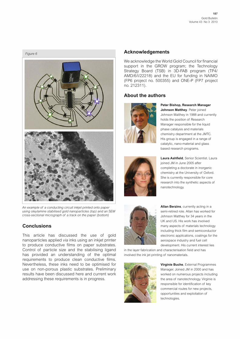
Figure 6 (top) depicts a conductive circuit where
OLEDs are powered via a central processing unit.
These films have been prepared from the gold-
oleylamine nanoparticles. SEM cross-section
analysis of the thermally cured film (Figure 6,
bottom) indicates a high degree of densification at
the surface of the paper and also the diffusion of
gold nanoparticles deep into the paper. This diffusion
into the polymer layers of the paper is thought to
contribute to the good adhesion observed.
It appears the lower volatility of the oleylamine
ligand does not adversely affect the conductive
properties on porous paper substrates. However,
higher process temperatures (above 200°C) are
required on non-porous plastic substrates to obtain
conductivity comparable to that achieved on paper.
Strategies are currently under investigation to lower
the process temperatures. Chemical treatments of
the substrate and film are areas of focus, together
with controlling particle size and morphology of the
gold nanoparticles. Use of non-amine containing
stabilising ligands is also under study.
Samples of gold inkjet printed onto smooth and texture paper,
top and bottom, respectively
Figure 5
Page 7
Gold Bulletin
Volume 43 No 3 2010
187
Conclusions
This article has discussed the use of gold
nanoparticles applied via inks using an inkjet printer
to produce conductive films on paper substrates.
Control of particle size and the stabilising ligand
has provided an understanding of the optimal
requirements to produce clean conductive films.
Nevertheless, these inks need to be optimised for
use on non-porous plastic substrates. Preliminary
results have been discussed here and current work
addressing these requirements is in progress.
Acknowledgements
We acknowledge the World Gold Council for financial
support in the GROW program; the Technology
Strategy Board (TSB) in 3D-FAB program (TP4/
AMD/6/I/22218) and the EU for funding in NAIMO
(FP6 project no. 500355) and ONE-P (FP7 project
no. 212311).
About the authors
Peter Bishop, Research Manager
Johnson Matthey. Peter joined
Johnson Matthey in 1988 and currently
holds the position of Research
Manager responsible for the liquid
phase catalysis and materials
chemistry department at the JMTC.
His group is engaged in a range of
catalytic, nano-material and glass
based research programs.
Laura Ashfield, Senior Scientist. Laura
joined JM in June 2005 after
completing a doctorate in inorganic
chemistry at the University of Oxford.
She is currently responsible for core
research into the synthetic aspects of
nanotechnology.
Allan Berzins, currently acting in a
semi-retired role. Allan has worked for
Johnson Matthey for 34 years in the
UK and US. His work has involved
many aspects of materials technology
including thick film and semiconductor
electronic applications, coatings for the
aerospace industry and fuel cell
development. His current interest lies
in the layer fabrication and characterisation field and has
involved the ink jet printing of nanomaterials.
Virginie Buche, External Programmes
Manager. Joined JM in 2000 and has
worked on numerous projects including
the area of nanotechnology. Virginie is
responsible for identification of key
commercial routes for new projects,
opportunities and exploitation of
technologies.
An example of a conducting circuit inkjet printed onto paper
using oleylamine stabilised gold nanoparticles (top) and an SEM
cross-sectional micrograph of a track on the paper (bottom)
Figure 6
Page 8
Gold Bulletin
Volume 43 No 3 2010
188
James Cookson, Senior Scientist.
James joined JM in 2005 after
completing a doctorate in chemistry at
the University of Oxford and working at
the Engineering and Physical Sciences
Research Council. His main interests
are in the synthesis of precious metal
nanoparticles and their application in
heterogeneous catalysis.
Ross Gordon, Research Scientist.
Joined JM in March 2009 after
completing a PhD in chemistry at the
University of Edinburgh. His current
research activities focus on printable
metal-based nanoparticle inks for
application as conductive thin films.
Carmen Salcianu, Research Scientist.
Carmen joined JM in March 2010. She
obtained her PhD degree from
Cambridge University, UK. Research
activities include the characterization
and the applications of nanomaterials
based on noble metals.
Patsy Sutton, Principal Scientist. Patsy
studied gold and silver compounds as
precursors for film deposition during
her PhD and has ten years experience
in gold inks for decorative applications.
References
1 Z. King, Plastic Electronics, The Advanced Institute of
Management Research, 2009
2 R. Das and P. Harrop, Printed, Organic & Flexible
Electronics Forecasts, Players & Opportunities 2009-2029,
IDTechEx, 2009
3 Y. Li and J. Hou, Major Classes of Conjugated Polymers
and Synthetic Strategies in Introduction to Organic
Electronics and Optoelectronic Materials and Devices, CRC
Press, Boca Raton, USA, 2008
4 N.N. Greenwood and A. Earnshaw, Chemistry of the
Elements, 1st ed, Pergamon Press Plc, Oxford, UK, 1990
5 A. A. R. Elshabini-Riad, Thin Film Technology Handbook,
McGraw-Hill Comp. Inc., USA, 1998
6 D. R. Gamota et. al., Printed Organic and Molecular
Electronics, Kluwer Academic Publishers, Massachusetts,
USA, 2004
7 OE-A Roadmap for Organic and Printed Electronics, 3rd
ed., ed. K. Hecker et. al., Organic Electronics Association,
Frankfurt, Germany, 2009
8 R. Della Torre, US005662573A
9 G. Schmidt, Proc. SPIE, 2006, 6336, 10
10 A. C. Huebler et. al., Org. Elect., 2007, 8, 480
11 K. Allen, Flexible Flat Displays, John Wiley & Sons Ltd.,
Chichester, UK, 2005
12 A. Gregg et. al., “Roll-to-Roll Manufacturing of Flexible
Displays” in Flexible Flat Panel Displays, ed. G. P. Crawford,
John Wiley & Sons, New York, USA, 2005
13 P. Calvert, Chem. Mater., 2001, 13, 3299
14 H. Sirringhaus et. al., Science, 2000, 290, 2123
15 H. Sirringhaus et. al., MRS Bull., 2003, 28, 802
16 D. Huang et. al., J. Electrochem. Soc., 2003, 150, G412
17 S. H. Ko et. al., Appl. Phys. Lett., 2007, 90, 141103
18 Z. Radivojevic et. al., Proc. 12th Intl. Workshop on Thermal
investigations of ICs, Nice, France, 2006
19. M. Gupta et. al., Scr. Mater., 2005, 52, 479
20 C. Corti and R. Holliday, Gold: Science and Applications,
CRC Press, USA, 2010
21 A.N. Papzian, Gold Bulletin, 1982, 15, 3
22 T. Bakhishev and V. Subramanian, J. Electron. Mat., 2009,
38, 2720
23 M. J. Coutts et. al., J. Phys. Chem. C, 2009, 113, 1325.
24 M. Aslam et. al., J. Mat. Chem., 2004, 14, 1795
25 D. V. Leff et. al., Langmuir, 1996, 12, 4723
26 Kumar et. al., Langmuir, 2003, 19, 6277
27 P. T. Bishop and V. Buche, WO2006/131766 A2
28 M. Brust et. al., J. Chem. Soc., Chem. Commun., 1994, 801
29 Y. Wu et. al., Chem. Mater., 2006, 18, 4627
30 J. D. Aiken and R. G. Finke, J. Mol. Catal. A: Chem., 1999,
145, 1
31 P.T. Bishop, A. Boardman and V. Buche, WO2007/110665 A2