24
Prof. Paolo Colantonio a.a. 2012‐13

Prof. Paolo Colantonioa.a. 2012‐13
Analogue ElectronicsProf. Paolo Colantonio 2 | 24
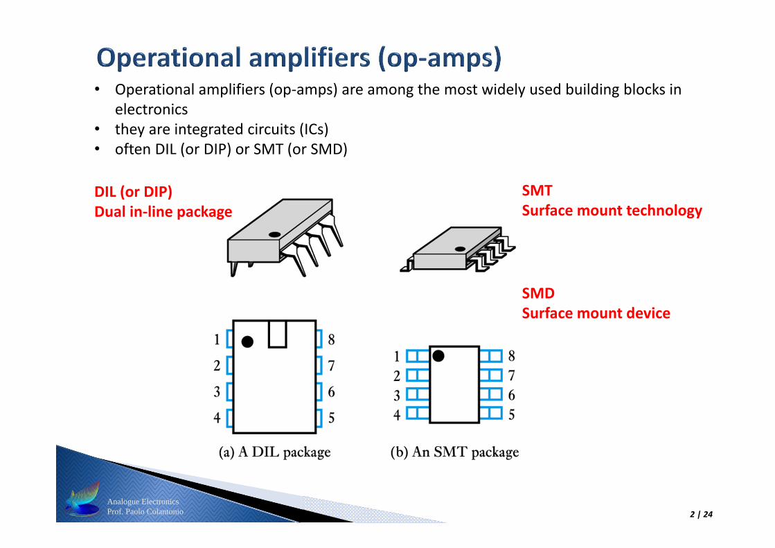
• Operational amplifiers (op‐amps) are among the most widely used building blocks in electronics
• they are integrated circuits (ICs)• often DIL (or DIP) or SMT (or SMD)
DIL (or DIP)Dual in‐line package
SMTSurface mount technology
SMDSurface mount device

Analogue ElectronicsProf. Paolo Colantonio 3 | 24
• A single package will often contain several op‐amps
Analogue ElectronicsProf. Paolo Colantonio 4 | 24
Equivalent circuit of an ideal op‐amp
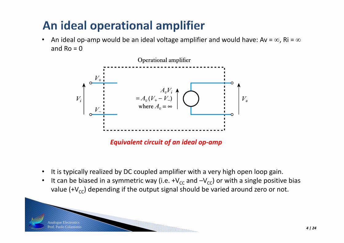
• An ideal op‐amp would be an ideal voltage amplifier and would have: Av = , Ri = and Ro = 0
• It is typically realized by DC coupled amplifier with a very high open loop gain.• It can be biased in a symmetric way (i.e. +VCC and –VCC) or with a single positive bias
value (+VCC) depending if the output signal should be varied around zero or not.

Analogue ElectronicsProf. Paolo Colantonio 5 | 24
v
cm
ACMRR
A
-
+
-
+
+V
-V
Ideal characteristicsa) Voltage Gain infinite Av=b) Input impedance infinite Zin= c) Output impedance null Zo=0d) Common Mode Rejection Ratio (CMRR) infinitee) Bandwidth infinite
2o v cm
v vv A v v A
0cmA
• In an ideal op‐amp it follows that the input current is null• If the output voltage is finite then the input voltage (V+‐V‐) is null (virtual earth)• The amplifier performance are not depending on the loading conditions• The bias voltages represent the minimum and maximum output voltage values• Being Av=, the output voltage of an op. amp. in an open loop configuration can
assume only one of the two saturating values (+VCC or –VCC)• The use of ideal components makes the analysis of these circuits very straightforward
Analogue ElectronicsProf. Paolo Colantonio 6 | 24
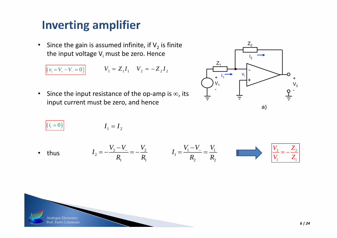
• Since the gain is assumed infinite, if V2 is finite the input voltage Vi must be zero. Hence
• thus
-
++V1-
Z2
Z1I2
I1
a)
vi+V2-
1 1 1 2 2 2V Z I V Z I 0iv V V
• Since the input resistance of the op‐amp is , its input current must be zero, and hence
0ii 21 II
2 2
1 1
V ZV Z
2 22
1 1
V V VIR R
1 1
12 2
V V VIR R

Analogue ElectronicsProf. Paolo Colantonio 7 | 24
• Consider the circuit with more inputs
• thus
0iv V V
• Since the input resistance of the op‐amp is , its input current must be zero, and hence
1 2 3 4I I I I
4 4 44 1 2 3
1 2 3
Z Z ZV V V VZ Z Z
11
1
VIR
-++
V1-
+V2-
+V3-
Z3
Z2
Z1
Z4
I1
I3
I4I2
b)
+V4- 0ii
• Since the input voltage is null (earth ground circuit)
22
2
VIR
33
3
VIR
44
4
VIR
• The output signal is a weighted sum of the input signals (considering Zi as resistances).
Analogue ElectronicsProf. Paolo Colantonio 8 | 24
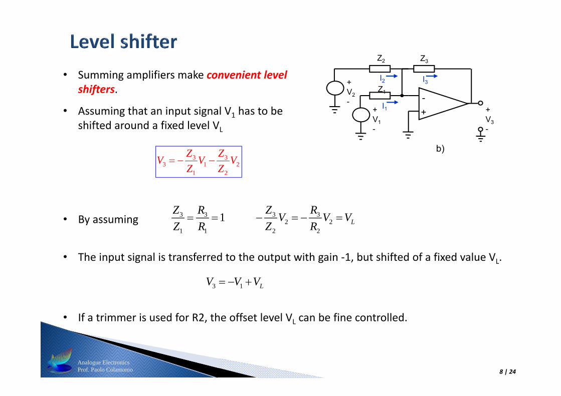
• Summing amplifiers make convenient level shifters.
• Assuming that an input signal V1 has to be shifted around a fixed level VL
3 33 1 2
1 2
Z ZV V VZ Z
-++
V1-
+V2-
Z1
Z3
I1
I3I2
b)
+V3-
• By assuming
• The input signal is transferred to the output with gain ‐1, but shifted of a fixed value VL.
Z2
3 3
1 1
1Z RZ R
3 32 2
2 2L
Z RV V VZ R
3 1 LV V V
• If a trimmer is used for R2, the offset level VL can be fine controlled.
Analogue ElectronicsProf. Paolo Colantonio 9 | 24
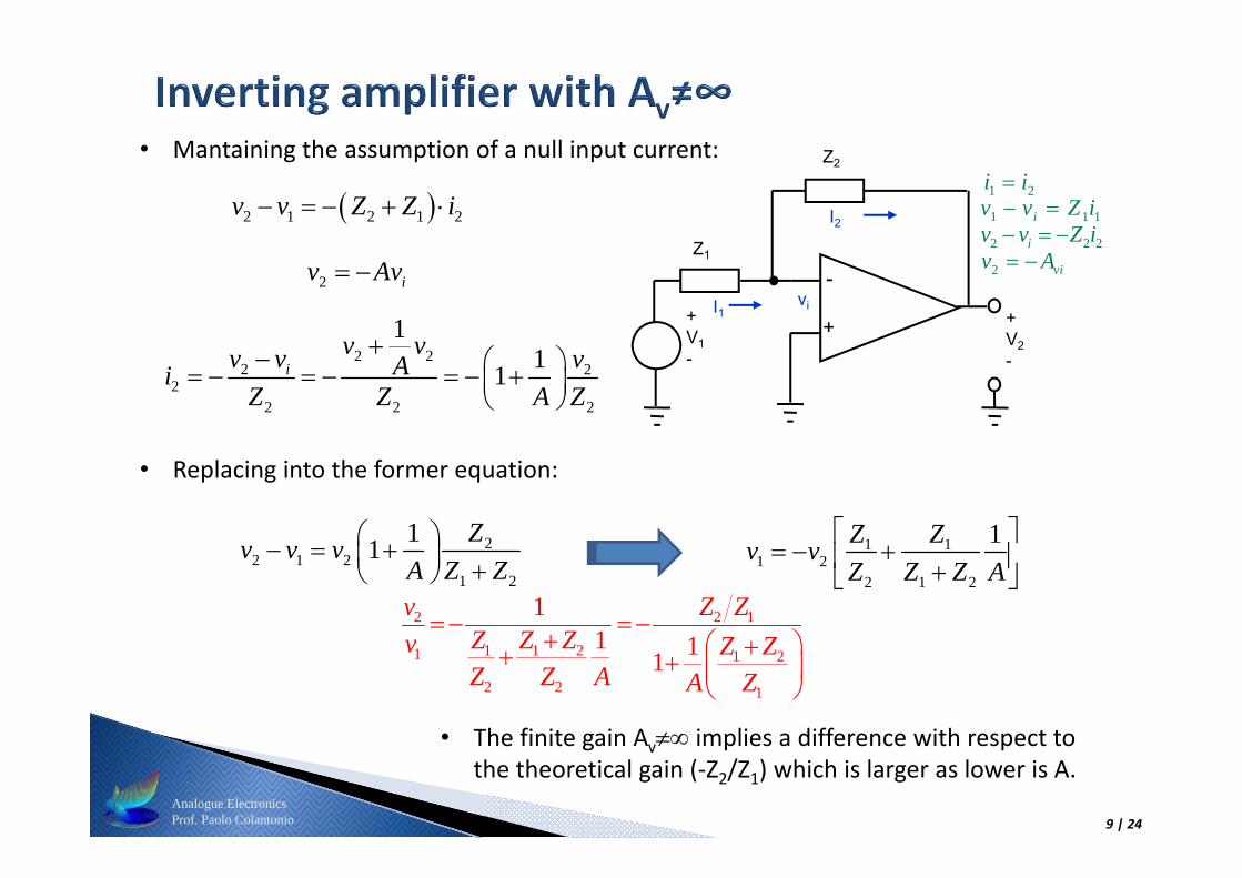
• Mantaining the assumption of a null input current:
+V2-
-
++V1-
Z2
Z1
I2
I1vi
2 1 2 1 2v v Z Z i 1 2i i1 1 1iv v Z i 2 2 2iv v Z i 2 viv A
2 iv Av
2 22 2
22 2 2
111i
v vv v vAiZ Z A Z
• Replacing into the former equation:
22 1 2
1 2
11 Zv v vA Z Z
1 1
1 22 1 2
1Z Zv vZ Z Z A
2 2 1
1 1 21 1 2
2 2 1
11 11
v Z ZZ Z Zv Z ZZ Z A A Z
• The finite gain Av implies a difference with respect to the theoretical gain (‐Z2/Z1) which is larger as lower is A.

Analogue ElectronicsProf. Paolo Colantonio 10 | 24
• Assuming a null input voltage and current 1v V 1
21 2
Zv VZ Z
1 2i i
+V2-
-
++V1-
Z2
Z1
I2
I1
121
12 v
ZZZ
v
• thus
2 2
1 1
1v Zv Z
• We can observe that assuming Z2=0 or Z1= the amplifier gain becomes unitary.• Thus we can realize an ideal buffer stage ideale (Rin=∞, Ro=0, Av=1) by using one of the
two following configurations:
-+
Z2=0
Z1
V1V2
-+
Z2
Z1=∞
V1V2

Analogue ElectronicsProf. Paolo Colantonio 11 | 24
o RV R I
R iI I
o iV R I

Analogue ElectronicsProf. Paolo Colantonio 12 | 24
• By using both the input ports of the opamp and by using the superposition principle:
+V3-
-
+
V1
R2
R1
V2R3
R4
I
NI
2 11 3
1 2 1 2
R Rv v vR R R R
42
3 4
Rv vR R
• Assuming the earth ground principle (V‐=V+):
1 2 4 23 2 1
3 4 1 1
R R R Rv v vR R R R
4 1 2 22 2
2 23 2 1
1 4 1 13 1
R R R Rv v vR R R
R v vR RR
R
2
431
324112
1
23 v
RRRRRRR
vvRRv
• Making a mathematical rearrangement
• Assuming v2v1, thus (v2+v1 )/2v1
3
4
1
2
RR
RR
1 4 2 32 1 2
3 2 11 1 3 4 2
R R R RR v vv v vR R R R
• If
1 4 2 3
1 3 4cm
R R R RAR R R
2 4
1 3
4 2
3 1
1v
cm
R RR RACMRR R RA
R R
23 2 1
1
Rv v vR
2
1v
RAR
Analogue ElectronicsProf. Paolo Colantonio 13 | 24
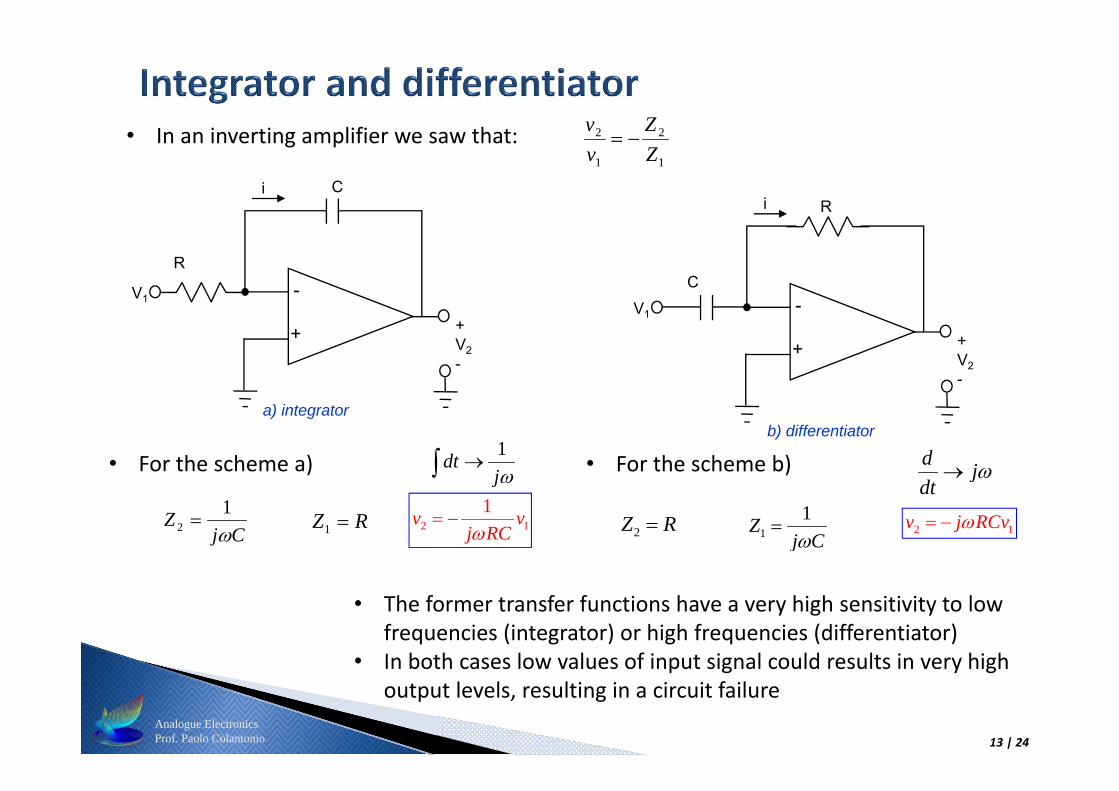
• In an inverting amplifier we saw that:1
2
1
2
ZZ
vv
+V2-
-
+
V1
C
R
i
a) integrator
• For the scheme a)
+V2-
-
+
V1
C
Ri
b) differentiator
CjZ
1
2 RZ 1 2 11v v
j RC
j
dt 1• For the scheme b)
2Z R 11Z
j C 2 1v j RCv
d jdt
• The former transfer functions have a very high sensitivity to low frequencies (integrator) or high frequencies (differentiator)
• In both cases low values of input signal could results in very high output levels, resulting in a circuit failure

Analogue ElectronicsProf. Paolo Colantonio 14 | 24
• In order to solve the frequency issues the previous circuits are modified as in the following
+V2-
-
+
C
R1
a) integrator
R2
V1 +V2-
-
+
V1
C
R2
b) differentiator
R1
2 2 2 2
1 1 1 2 1
1 11 1
H
v Z R Rfv Z R j R C R jf
2 2 2 2
1 1 1 1
1
1 111 1 L
v Z R Rfv Z R R
j R C jf
• The insertion of a resistor modifies the frequency behaviour avoiding the answer to increase indefinitely towards infinity
• Practically the bandwidth has been modified in the upper (case a) or in the lower (case b) frequency range

Analogue ElectronicsProf. Paolo Colantonio 15 | 24
+V2-
-
+
C
R1
a) integrator
R2
V1
2
1
1
1v
H
RA fR jf
22
1
120log 20log
1
v dB
H
RAR f
f
2 2
12Hf R C
where
vH
fA arctgf
|Av|
3 dB
fs log(f)
fs log(f)
Av180°
90°
45°
• Comparing the result with the response of a Low‐Pass RC filter
V1
R2C V2
2
1
1
1v
H
vA fv jf
2
12Hf R C
2
120log
1
v dB
H
Aff
vH
fA arctgf
• The real integrator behaves like a Low‐Pass RC filter• The group R2C limits the opamp bandwidht, which
output is proportional to the input up to fH, while for f>fHit integrates the input signal.
2
1
1H v H
Rf f A fj f R
2
1H v
Rf f AR

Analogue ElectronicsProf. Paolo Colantonio 16 | 24
2
1
1
1v
L
RA fRjf
22
1
120log 20log
1v dB
L
RAR f
f
1 1
12Lf R C
where
Lv
fA arctgf
• Comparing the result with the response of a High‐Pass RC filter
2
1
1
1v
L
vA fvjf
1
12Lf R C
2
120log
1v dB
L
Aff
Lv
fA arctgf
• The real differentiator behaves like a High‐Pass RC filter• The group R1C limits the opamp bandwidht, which
output is the differentiation of the input up to fL, while for f>fL it is simply proportional to the input signal.
2
1L v
Rf f AR
2
1
1L v
L
Rf f A j ff R
+V2-
-
+
V1
C
R2
b) differentiator
R1
3 dB
fi log(f)
fs log(f)
270°
180°
45°
Av V1R2
C
V2

Analogue ElectronicsProf. Paolo Colantonio 17 | 24
• The previous schemes can be combined to limit the opamp bandwidth as reported in the following scheme
+V2-
-
+
V1
C1 R2R1
C2
2
1
VGV
22 2
1
1 120log 20log 20log
11 L
H
RA fR ff
ff
L
H
ffA f arctg arctgf f
1 1
12Lf R C
2 2
12Hf R C
log(f)
20 dBdec 20 dB
dec
Lf HfBandwidth
• (fH‐fL) is the bandwidth of the resulting amplifier

Analogue ElectronicsProf. Paolo Colantonio 18 | 24
• So far we have assumed the use of ideal op‐amps• these have Av=, Ri= and Ro=0
• Real components do not have these ideal characteristics (though in many cases they approximate to them)
• In this section we will look at the characteristics of typical devices• perhaps the most widely used general purpose op‐amp is the 741

Analogue ElectronicsProf. Paolo Colantonio 19 | 24
Voltage gain• typical gain of an operational amplifier might be 100 – 140 dB (voltage gain of 105–106)• 741 has a typical gain of 106 dB (2 105)• high gain devices might have a gain of 160 dB (108)• while not infinite, the gain of most op‐amps is ‘high‐enough’• however, gain varies between devices and with temperature
Input resistance• typical input resistance of a 741 is 2 M• very variable, for a 741 it can be as low as 300 k• the above value is typical for devices based on bipolar transistors• op‐amps based on field‐effect transistors generally have a much higher input
resistance – perhaps 1012 • we will discuss bipolar and field‐effect transistors later
Output resistance• typical output resistance of a 741 is 75 • again very variable• often of more importance, is the maximum output current the 741 will supply 20 mA• high‐power devices may supply an amp or more
Analogue ElectronicsProf. Paolo Colantonio 20 | 24
Supply voltage range• a typical arrangement would use supply voltages of +15V and – 15V, but a wide
range of supply voltages is usually possible• the 741 can use voltages in the range 5 to 18V• some devices allow voltages up to 30V or more• others, designed for low voltages, may use 1.5V• many op‐amps permit single voltage supply operation, typically in the range 4 to 30V
Common‐mode rejection ratio• an ideal op‐amp would not respond to common‐mode signals• real amplifiers do respond to some extent• the common‐mode rejection ratio (CMRR) is the ratio of the response produced by a
differential‐mode signal to that produced by a common‐mode signal• typical values for CMRR might be in the range 80 to 120 dB
• 741 has a CMRR of about 90 dB

Analogue ElectronicsProf. Paolo Colantonio 21 | 24
Frequency response• typical 741 frequency response is shown here• upper cut‐off frequency is a few hertz• frequency range generally described by the unity‐gain bandwidth• high‐speed devices may operate up to several gigahertz

Analogue ElectronicsProf. Paolo Colantonio 22 | 24
• Our analysis assumed the use of an ideal op‐amp• When using real components we need to ensure that our assumptions are valid• In general this will be true if we:
• limit the gain of our circuit to much less than the open‐loop gain of our op‐amp
• choose external resistors that are small compared with the input resistance of the op‐amp
• choose external resistors that are large compared with the output resistance of the op‐amp
• Generally we use resistors in the range 1 to 100 k
Analogue ElectronicsProf. Paolo Colantonio 23 | 24
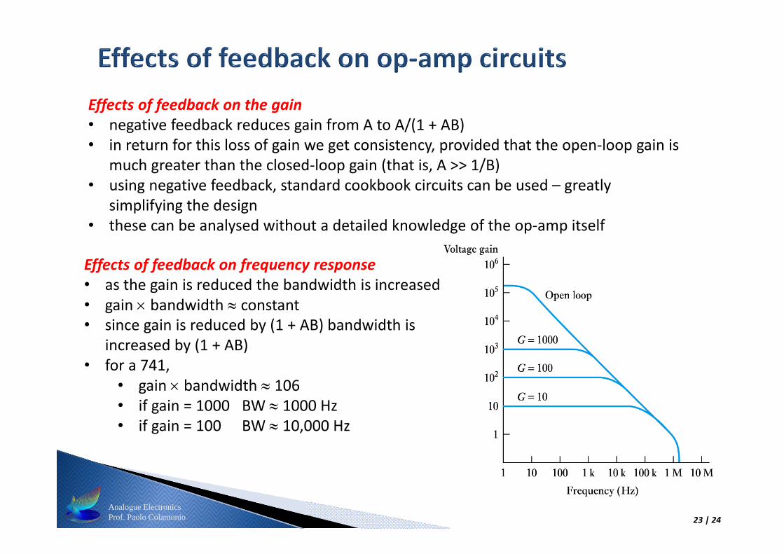
Effects of feedback on the gain• negative feedback reduces gain from A to A/(1 + AB)• in return for this loss of gain we get consistency, provided that the open‐loop gain is
much greater than the closed‐loop gain (that is, A >> 1/B)• using negative feedback, standard cookbook circuits can be used – greatly
simplifying the design• these can be analysed without a detailed knowledge of the op‐amp itself
Effects of feedback on frequency response• as the gain is reduced the bandwidth is increased• gain bandwidth constant• since gain is reduced by (1 + AB) bandwidth is
increased by (1 + AB)• for a 741,
• gain bandwidth 106• if gain = 1000 BW 1000 Hz• if gain = 100 BW 10,000 Hz

Analogue ElectronicsProf. Paolo Colantonio 24 | 24
Effects of feedback on input and output resistance• input/output resistance can be increased or decreased depending on how feedback
is used• in each case the resistance is changed by a factor of (1 + AB)
• Example: if an op‐amp with a gain of 2x10⁵ is used to produce an amplifier with a gain of 100 then:
• A = 2 x 10⁵• B = 1/G = 0.01• (1 + AB) = (1 + 2000) 2000


