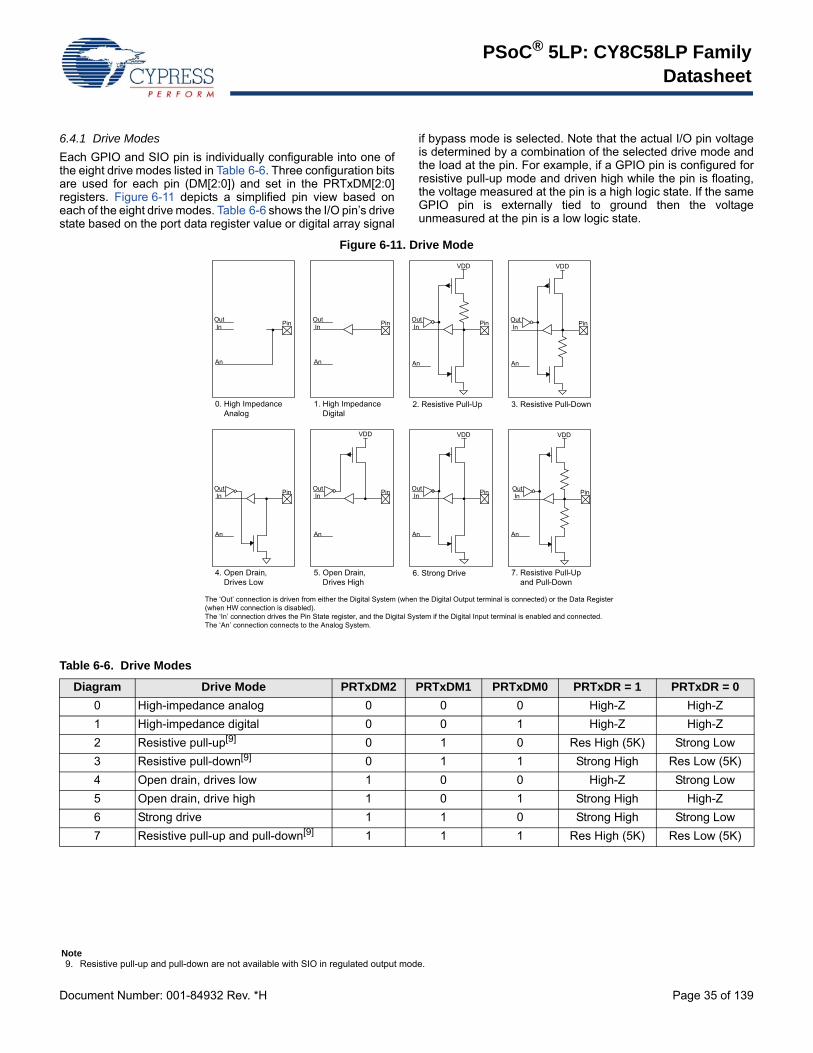
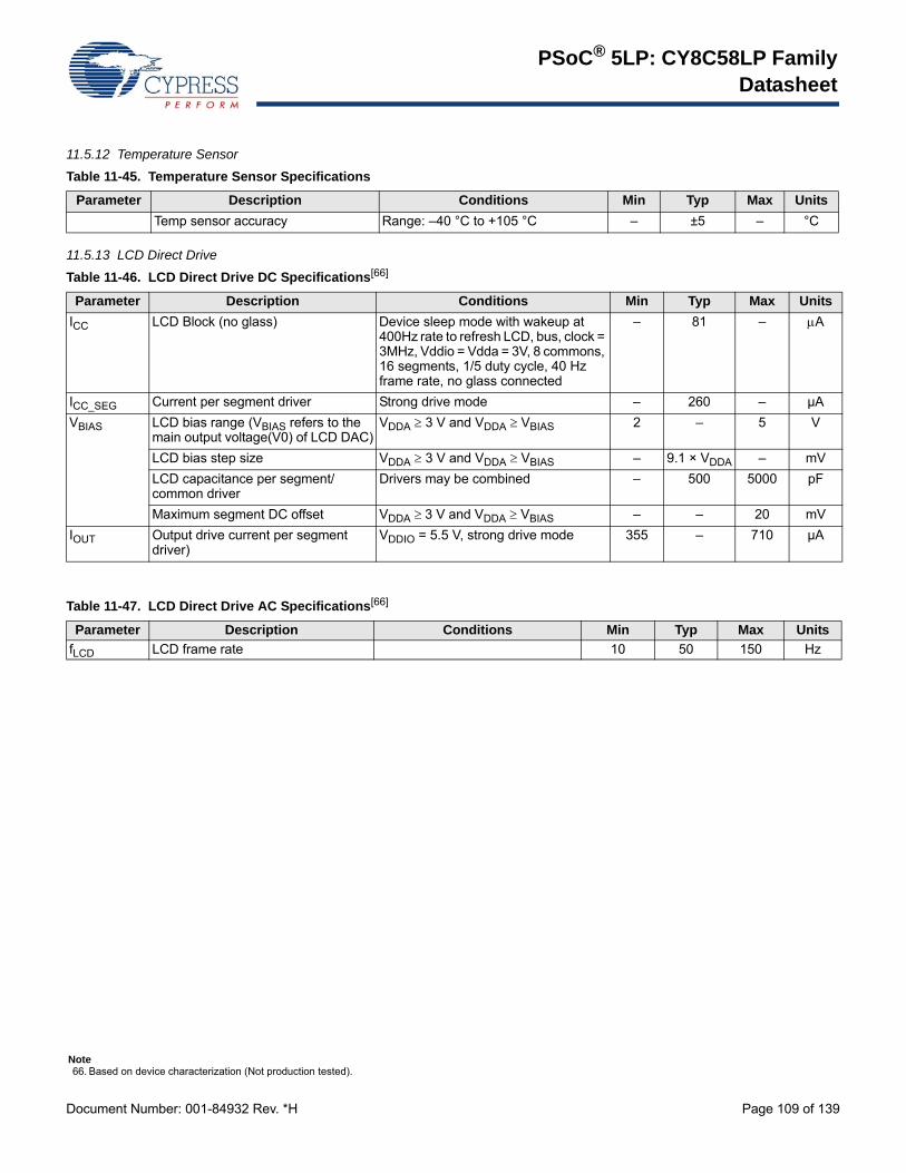
PSoC ® 5LP: CY8C58LP Family Datasheet Programmable System-on-Chip (PSoC ® ) Cypress Semiconductor Corporation • 198 Champion Court • San Jose, CA 95134-1709 • 408-943-2600 Document Number: 001-84932 Rev. *H Revised March 24, 2015 General Description PSoC ® 5LP is a true programmable embedded system-on-chip, integrating configurable analog and digital peripherals, memory, and a microcontroller on a single chip. The PSoC 5LP architecture boosts performance through: 32-bit ARM Cortex-M3 core plus DMA controller and digital filter processor, at up to 80 MHz Ultra low power with industry's widest voltage range Programmable digital and analog peripherals enable custom functions Flexible routing of any analog or digital peripheral function to any pin PSoC devices employ a highly configurable system-on-chip architecture for embedded control design. They integrate configurable analog and digital circuits, controlled by an on-chip microcontroller. A single PSoC device can integrate as many as 100 digital and analog peripheral functions, reducing design time, board space, power consumption, and system cost while improving system quality. Features Operating characteristics Voltage range: 1.71 to 5.5 V, up to 6 power domains Temperature range (ambient): –40 to 85 °C [1] Extended temperature parts: –40 to 105 °C DC to 80-MHz operation Power modes • Active mode 3.1 mA at 6 MHz, and 15.4 mA at 48 MHz • 2-μA sleep mode • 300-nA hibernate mode with RAM retention Boost regulator from 0.5-V input up to 5-V output Performance 32-bit ARM Cortex-M3 CPU, 32 interrupt inputs 24-channel direct memory access (DMA) controller 24-bit 64-tap fixed-point digital filter processor (DFB) Memories Up to 256 KB program flash, with cache and security features Up to 32 KB additional flash for error correcting code (ECC) Up to 64 KB RAM 2 KB EEPROM Digital peripherals Four 16-bit timer, counter, and PWM (TCPWM) blocks I 2 C, 1 Mbps bus speed USB 2.0 certified Full-Speed (FS) 12 Mbps peripheral inter- face (TID#10840032) using internal oscillator [2] Full CAN 2.0b, 16 Rx, 8 Tx buffers 20 to 24 universal digital blocks (UDB), programmable to create any number of functions: • 8-, 16-, 24-, and 32-bit timers, counters, and PWMs •I 2 C, UART, SPI, I2S, LIN 2.0 interfaces • Cyclic redundancy check (CRC) • Pseudo random sequence (PRS) generators • Quadrature decoders • Gate-level logic functions Programmable clocking 3- to 74-MHz internal oscillator, 1% accuracy at 3 MHz 4- to 25-MHz external crystal oscillator Internal PLL clock generation up to 80 MHz Low-power internal oscillator at 1, 33, and 100 kHz 32.768-kHz external watch crystal oscillator 12 clock dividers routable to any peripheral or I/O Analog peripherals Configurable 8- to 20-bit delta-sigma ADC Up to two 12-bit SAR ADCs Four 8-bit DACs Four comparators Four opamps Four programmable analog blocks, to create: • Programmable gain amplifier (PGA) • Transimpedance amplifier (TIA) • Mixer • Sample and hold circuit CapSense ® support, up to 62 sensors 1.024 V ±0.1% internal voltage reference Versatile I/O system 46 to 72 I/O pins – up to 62 general-purpose I/Os (GPIOs) Up to eight performance I/O (SIO) pins • 25 mA current sink • Programmable input threshold and output high voltages • Can act as a general-purpose comparator • Hot swap capability and overvoltage tolerance Two USBIO pins that can be used as GPIOs Route any digital or analog peripheral to any GPIO LCD direct drive from any GPIO, up to 46 × 16 segments CapSense support from any GPIO 1.2-V to 5.5-V interface voltages, up to four power domains Programming, debug, and trace JTAG (4-wire), serial wire debug (SWD) (2-wire), single wire viewer (SWV), and Traceport (5-wire) interfaces ARM debug and trace modules embedded in the CPU core Bootloader programming through I 2 C, SPI, UART, USB, and other interfaces Package options: 68-pin QFN and 100-pin TQFP Development support with free PSoC Creator™ tool Schematic and firmware design support Over 100 PSoC Components™ integrate multiple ICs and system interfaces into one PSoC. Components are free embedded ICs represented by icons. Drag and drop component icons to design systems in PSoC Creator. Includes free GCC compiler, supports Keil/ARM MDK compiler Supports device programming and debugging Notes 1. The maximum storage temperature is 150 °C in compliance with JEDEC Standard JESD22-A103, High Temperature Storage Life. 2. This feature on select devices only. See Ordering Information on page 126 for details.
Transcript
PSoC® 5LP: CY8C58LP FamilyDatasheet
Programmable System-on-Chip (PSoC®)
Cypress Semiconductor Corporation • 198 Champion Court • San Jose, CA 95134-1709 • 408-943-2600Document Number: 001-84932 Rev. *H Revised March 24, 2015
General DescriptionPSoC® 5LP is a true programmable embedded system-on-chip, integrating configurable analog and digital peripherals, memory, anda microcontroller on a single chip. The PSoC 5LP architecture boosts performance through:
32-bit ARM Cortex-M3 core plus DMA controller and digital filter processor, at up to 80 MHz
Ultra low power with industry's widest voltage range
Programmable digital and analog peripherals enable custom functions
Flexible routing of any analog or digital peripheral function to any pin
PSoC devices employ a highly configurable system-on-chip architecture for embedded control design. They integrate configurableanalog and digital circuits, controlled by an on-chip microcontroller. A single PSoC device can integrate as many as 100 digital andanalog peripheral functions, reducing design time, board space, power consumption, and system cost while improving system quality.
FeaturesOperating characteristics Voltage range: 1.71 to 5.5 V, up to 6 power domains Temperature range (ambient): –40 to 85 °C [1]
Extended temperature parts: –40 to 105 °C DC to 80-MHz operation Power modes
• Active mode 3.1 mA at 6 MHz, and 15.4 mA at 48 MHz• 2-µA sleep mode• 300-nA hibernate mode with RAM retention
Boost regulator from 0.5-V input up to 5-V output
Performance 32-bit ARM Cortex-M3 CPU, 32 interrupt inputs 24-channel direct memory access (DMA) controller 24-bit 64-tap fixed-point digital filter processor (DFB)
Memories Up to 256 KB program flash, with cache and security features Up to 32 KB additional flash for error correcting code (ECC) Up to 64 KB RAM 2 KB EEPROM
Digital peripherals Four 16-bit timer, counter, and PWM (TCPWM) blocks I2C, 1 Mbps bus speed USB 2.0 certified Full-Speed (FS) 12 Mbps peripheral inter-
face (TID#10840032) using internal oscillator[2]
Full CAN 2.0b, 16 Rx, 8 Tx buffers 20 to 24 universal digital blocks (UDB), programmable to
create any number of functions:• 8-, 16-, 24-, and 32-bit timers, counters, and PWMs• I2C, UART, SPI, I2S, LIN 2.0 interfaces• Cyclic redundancy check (CRC)• Pseudo random sequence (PRS) generators• Quadrature decoders• Gate-level logic functions
Programmable clocking 3- to 74-MHz internal oscillator, 1% accuracy at 3 MHz 4- to 25-MHz external crystal oscillator Internal PLL clock generation up to 80 MHz Low-power internal oscillator at 1, 33, and 100 kHz 32.768-kHz external watch crystal oscillator 12 clock dividers routable to any peripheral or I/O
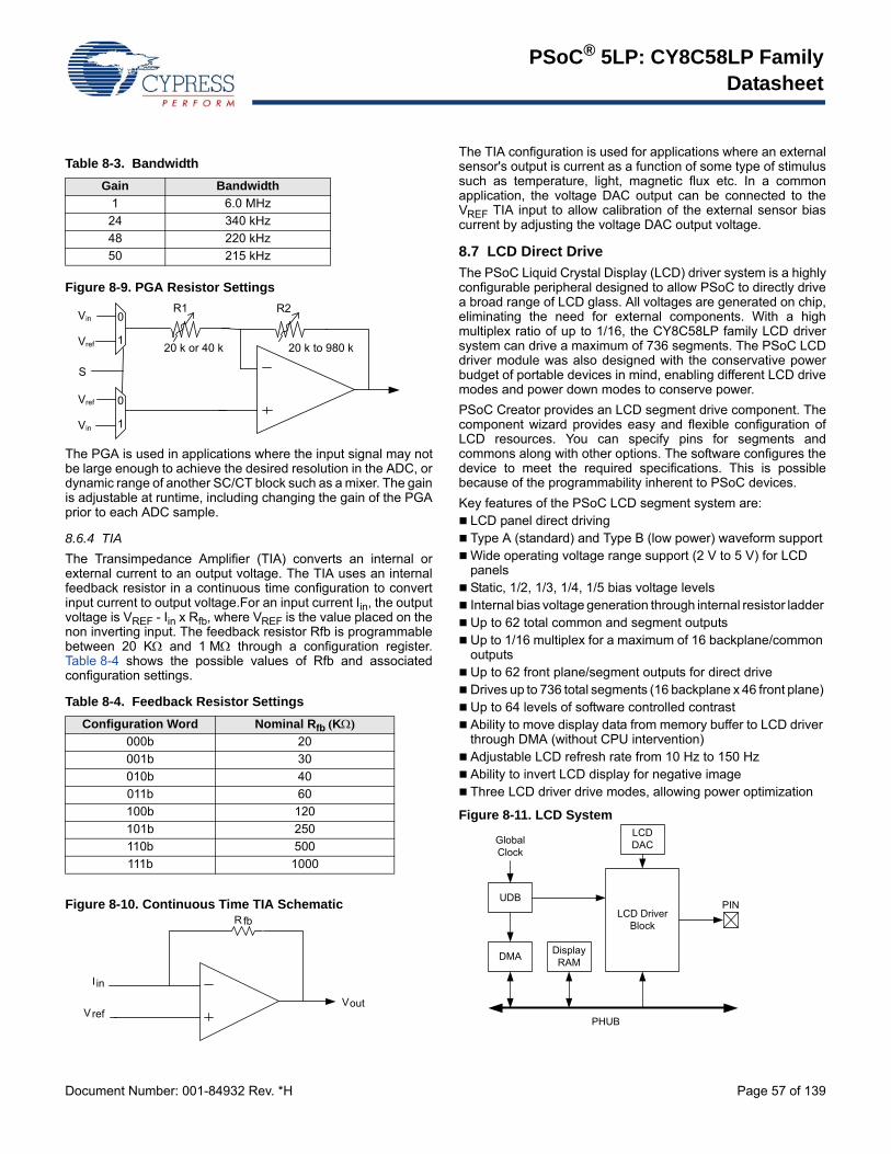
Analog peripherals Configurable 8- to 20-bit delta-sigma ADC Up to two 12-bit SAR ADCs Four 8-bit DACs Four comparators Four opamps Four programmable analog blocks, to create:
• Programmable gain amplifier (PGA)• Transimpedance amplifier (TIA)• Mixer• Sample and hold circuit
CapSense® support, up to 62 sensors 1.024 V ±0.1% internal voltage reference
Versatile I/O system 46 to 72 I/O pins – up to 62 general-purpose I/Os (GPIOs) Up to eight performance I/O (SIO) pins
• 25 mA current sink• Programmable input threshold and output high voltages• Can act as a general-purpose comparator• Hot swap capability and overvoltage tolerance
Two USBIO pins that can be used as GPIOs Route any digital or analog peripheral to any GPIO LCD direct drive from any GPIO, up to 46 × 16 segments CapSense support from any GPIO 1.2-V to 5.5-V interface voltages, up to four power domains
Programming, debug, and trace JTAG (4-wire), serial wire debug (SWD) (2-wire), single wire
viewer (SWV), and Traceport (5-wire) interfaces ARM debug and trace modules embedded in the CPU core Bootloader programming through I2C, SPI, UART, USB, and
other interfaces
Package options: 68-pin QFN and 100-pin TQFP
Development support with free PSoC Creator™ tool Schematic and firmware design support Over 100 PSoC Components™ integrate multiple ICs and
system interfaces into one PSoC. Components are free embedded ICs represented by icons. Drag and drop component icons to design systems in PSoC Creator.
Includes free GCC compiler, supports Keil/ARM MDK compiler
Supports device programming and debugging
Notes1. The maximum storage temperature is 150 °C in compliance with JEDEC Standard JESD22-A103, High Temperature Storage Life.2. This feature on select devices only. See Ordering Information on page 126 for details.
PSoC® 5LP: CY8C58LP FamilyDatasheet
Document Number: 001-84932 Rev. *H Page 2 of 139
More InformationCypress provides a wealth of data at www.cypress.com to help you to select the right PSoC device for your design, and to help youto quickly and effectively integrate the device into your design. For a comprehensive list of resources, see the knowledge base articleKBA86521, How to Design with PSoC 3, PSoC 4, and PSoC 5LP. Following is an abbreviated list for PSoC 5LP:
Overview: PSoC Portfolio, PSoC Roadmap
Product Selectors: PSoC 1, PSoC 3, PSoC 4, PSoC 5LPIn addition, PSoC Creator includes a device selection tool.
Application notes: Cypress offers a large number of PSoC application notes covering a broad range of topics, from basic to advanced level. Recommended application notes for getting started with PSoC 5LP are: AN77759: Getting Started With PSoC 5LP AN77835: PSoC 3 to PSoC 5LP Migration Guide AN61290: Hardware Design Considerations AN57821: Mixed Signal Circuit Board Layout AN58304: Pin Selection for Analog Designs AN81623: Digital Design Best Practices AN73854: Introduction To Bootloaders
Development Kits: CY8CKIT-001 provides a common development platform for
any one of the PSoC 1, PSoC 3, PSoC 4, or PSoC 5LP families of devices.
CY8CKIT-050 is designed for analog performance. It enables you to evaluate, develop and prototype high precision analog, low-power and low-voltage applications powered by PSoC 5LP.
Both kits support the PSoC Expansion Board Kit ecosystem. Expansion kits are available for a number of applications including CapSense, precision temperature measurement, and power supervision.
The MiniProg3 device provides an interface for flash programming and debug.
PSoC Creator
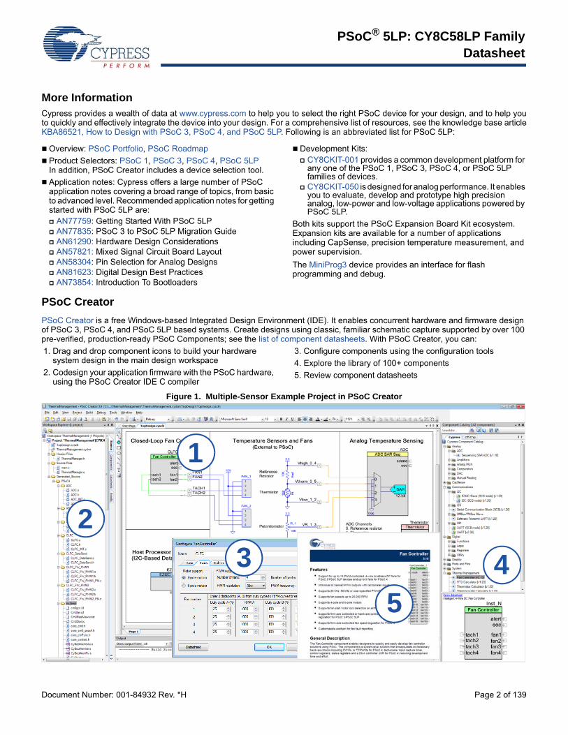
PSoC Creator is a free Windows-based Integrated Design Environment (IDE). It enables concurrent hardware and firmware design of PSoC 3, PSoC 4, and PSoC 5LP based systems. Create designs using classic, familiar schematic capture supported by over 100 pre-verified, production-ready PSoC Components; see the list of component datasheets. With PSoC Creator, you can:
1. Drag and drop component icons to build your hardware system design in the main design workspace
2. Codesign your application firmware with the PSoC hardware, using the PSoC Creator IDE C compiler
3. Configure components using the configuration tools
4. Explore the library of 100+ components
5. Review component datasheets
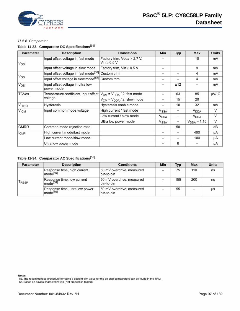
Figure 1. Multiple-Sensor Example Project in PSoC Creator
4. CPU ............................................................................... 124.1 ARM Cortex-M3 CPU ...........................................124.2 Cache Controller ..................................................134.3 DMA and PHUB ...................................................134.4 Interrupt Controller ...............................................16
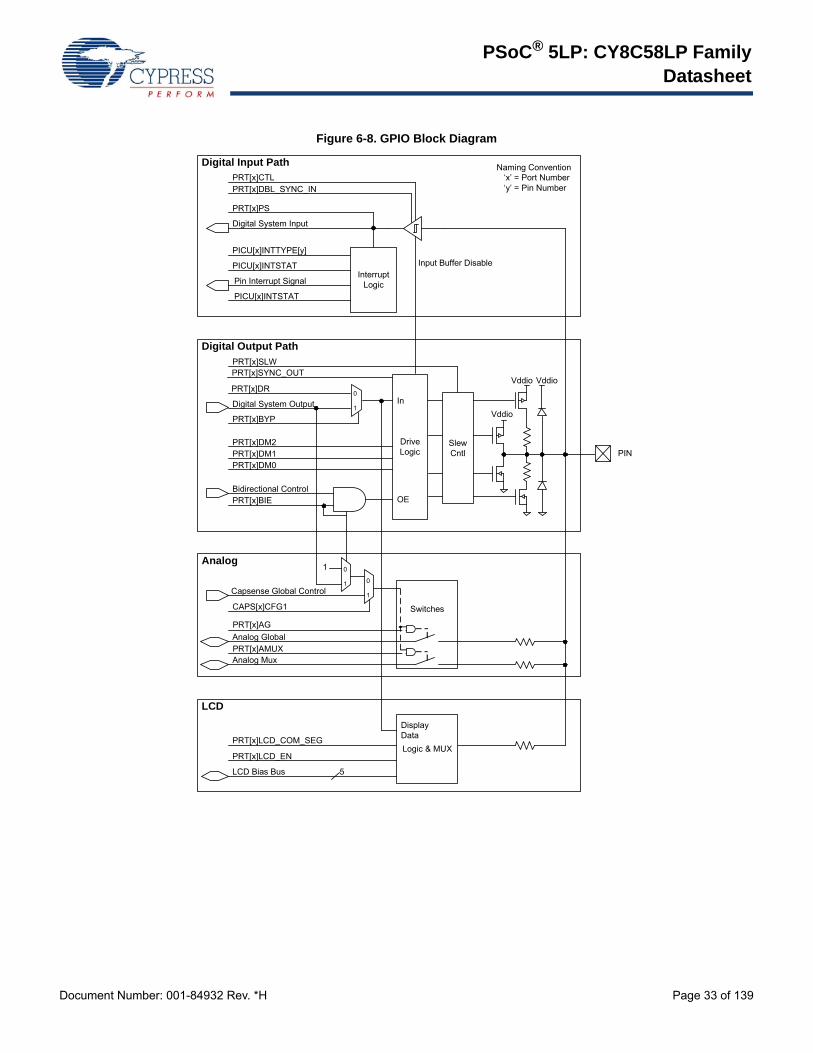
6. System Integration ...................................................... 226.1 Clocking System ...................................................226.2 Power System ......................................................256.3 Reset ....................................................................306.4 I/O System and Routing .......................................32
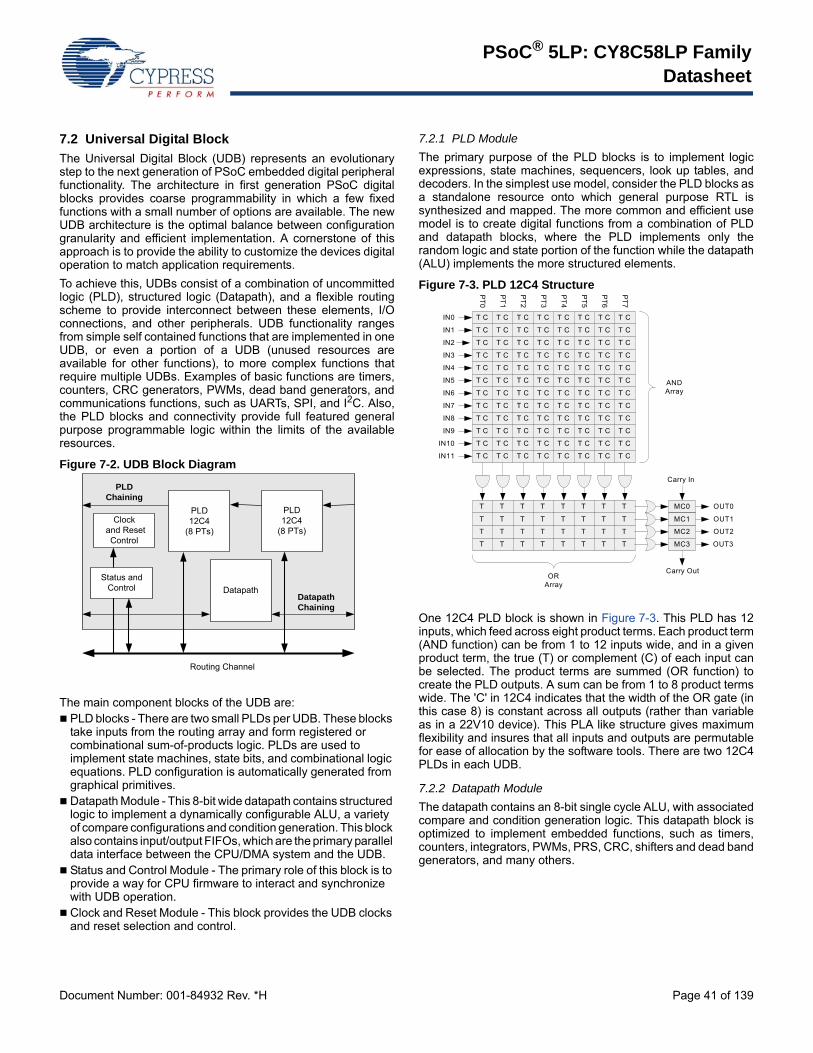
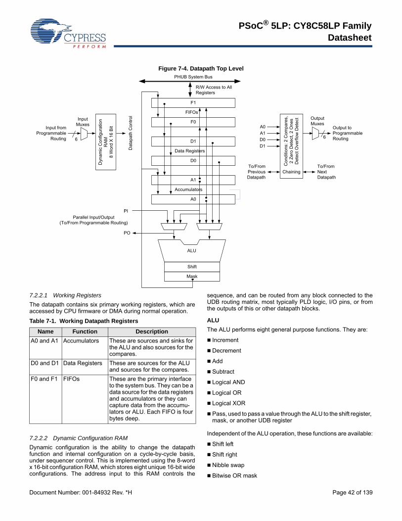
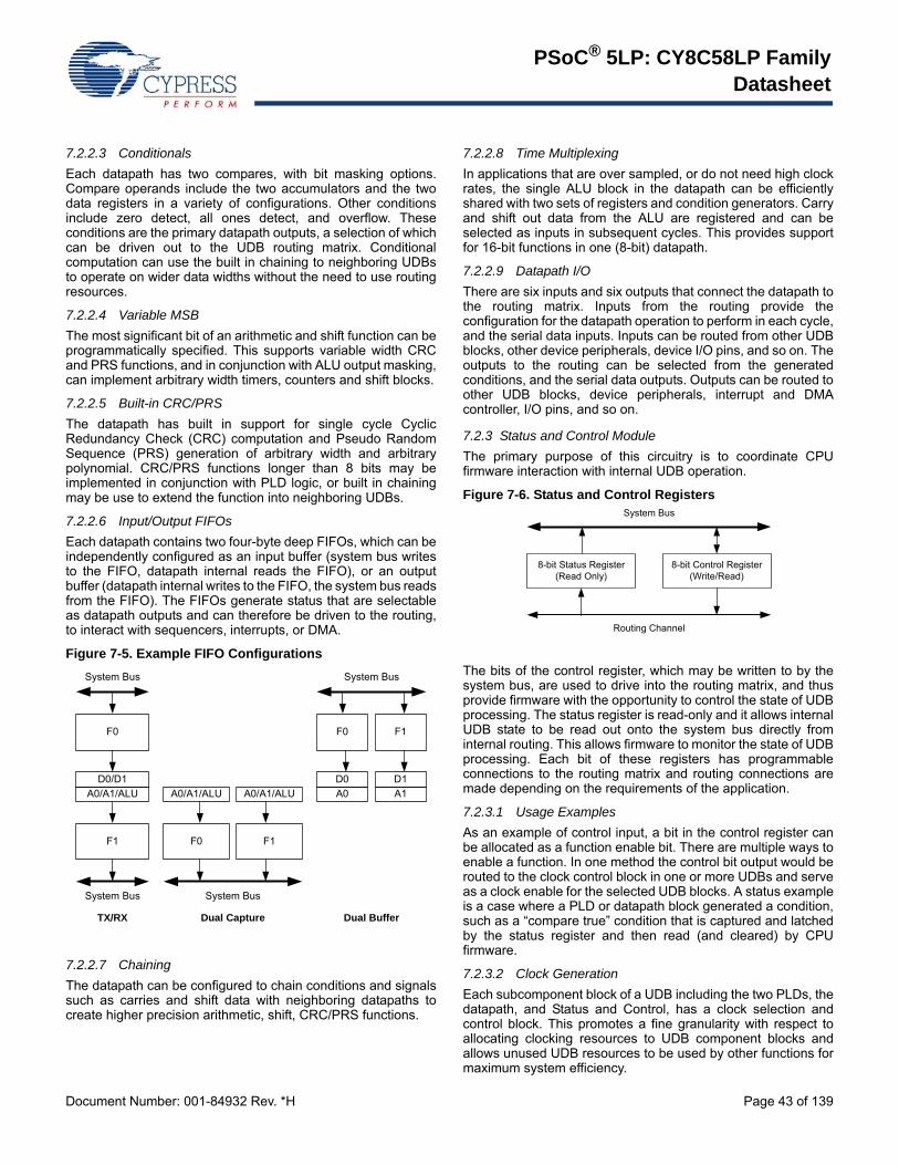
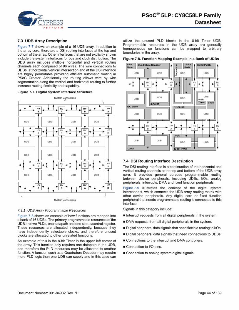
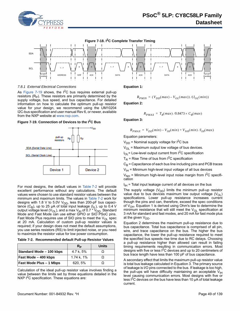
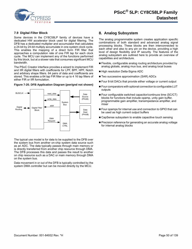
7. Digital Subsystem ....................................................... 397.1 Example Peripherals ............................................397.2 Universal Digital Block ..........................................417.3 UDB Array Description .........................................447.4 DSI Routing Interface Description ........................447.5 CAN ......................................................................467.6 USB ......................................................................477.7 Timers, Counters, and PWMs ..............................487.8 I2C ........................................................................487.9 Digital Filter Block .................................................50
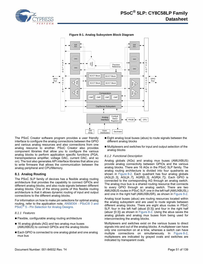
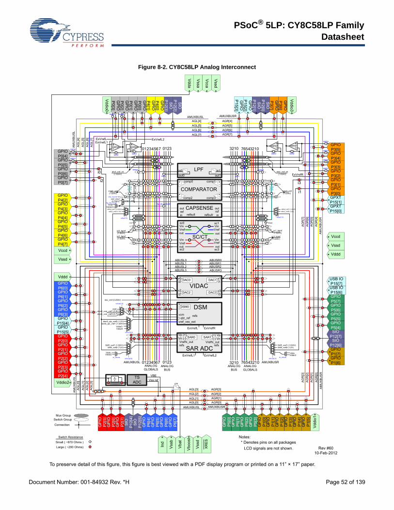
8. Analog Subsystem ...................................................... 508.1 Analog Routing .....................................................518.2 Delta-sigma ADC ..................................................538.3 Successive Approximation ADC ...........................548.4 Comparators .........................................................548.5 Opamps ................................................................568.6 Programmable SC/CT Blocks ..............................568.7 LCD Direct Drive ..................................................578.8 CapSense .............................................................588.9 Temp Sensor ........................................................588.10 DAC ....................................................................588.11 Up/Down Mixer ...................................................598.12 Sample and Hold ................................................59
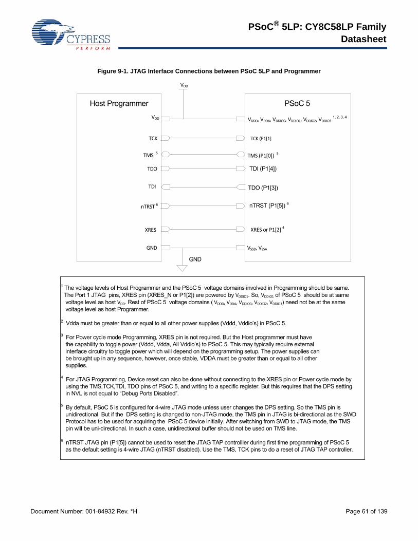
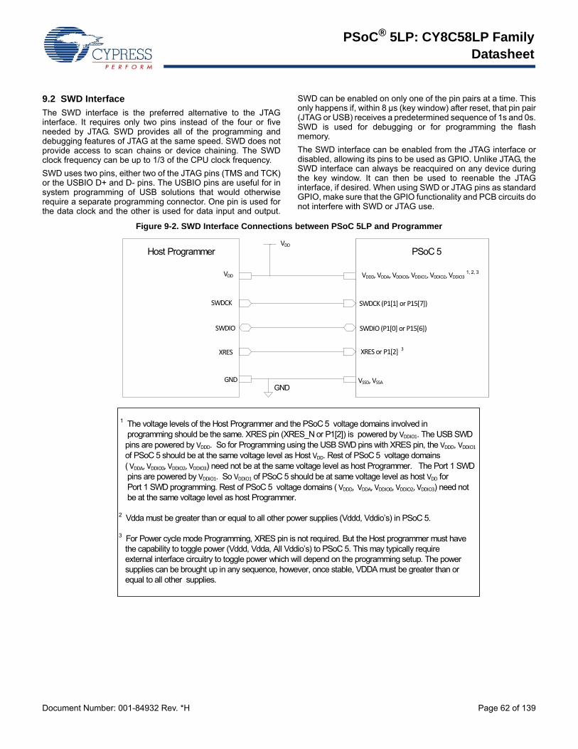
9. Programming, Debug Interfaces, Resources ............ 609.1 JTAG Interface .....................................................609.2 SWD Interface ......................................................629.3 Debug Features ....................................................639.4 Trace Features .....................................................639.5 SWV and TRACEPORT Interfaces ......................639.6 Programming Features .........................................639.7 Device Security ....................................................63
10. Development Support ............................................... 6410.1 Documentation ...................................................6410.2 Online .................................................................6410.3 Tools ...................................................................64
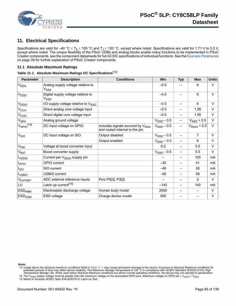
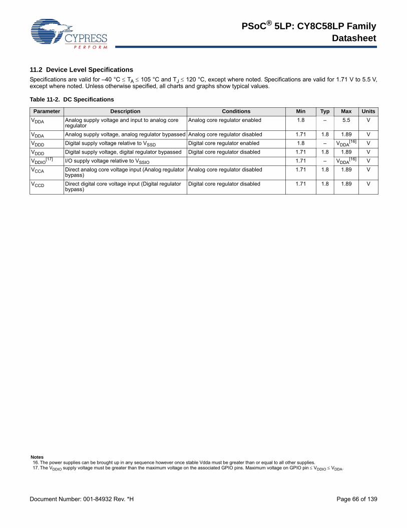
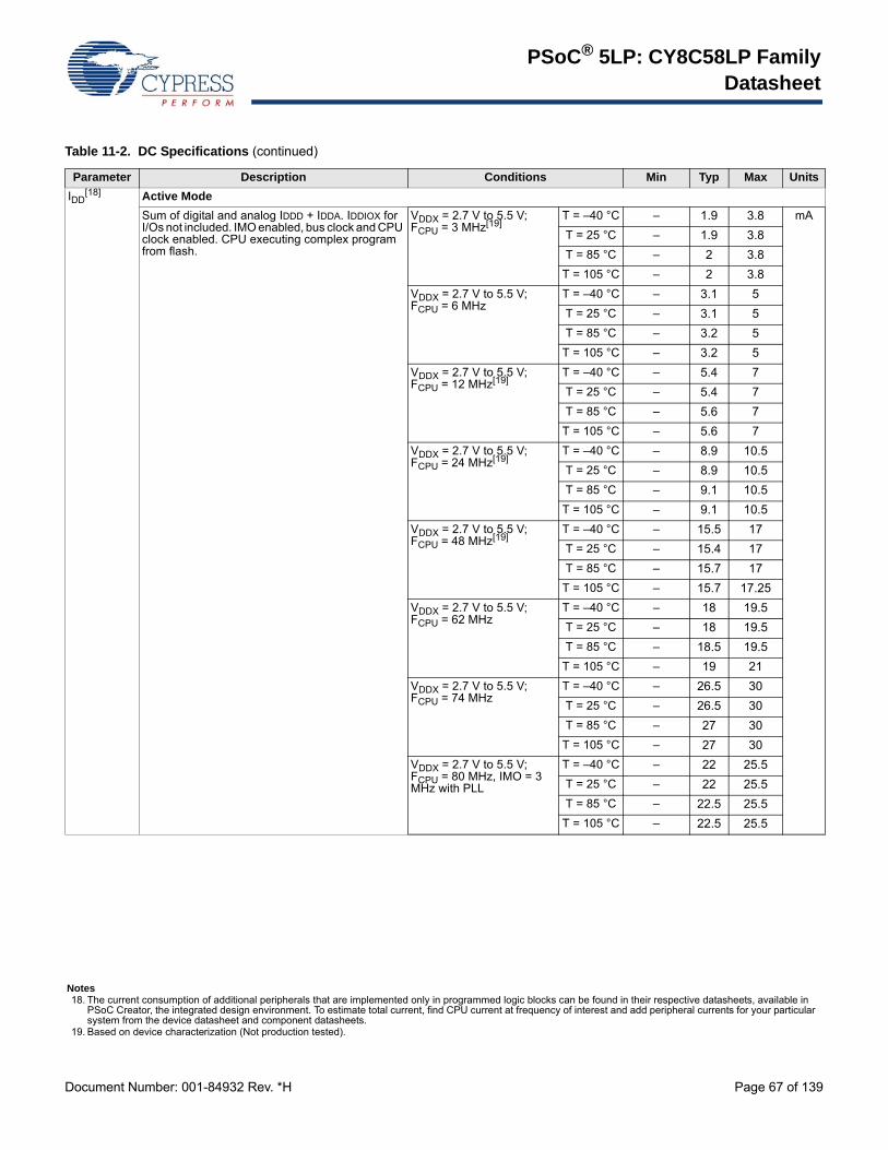
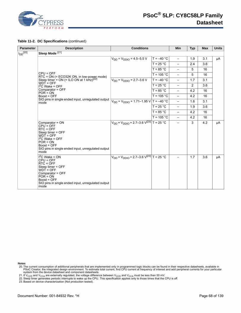
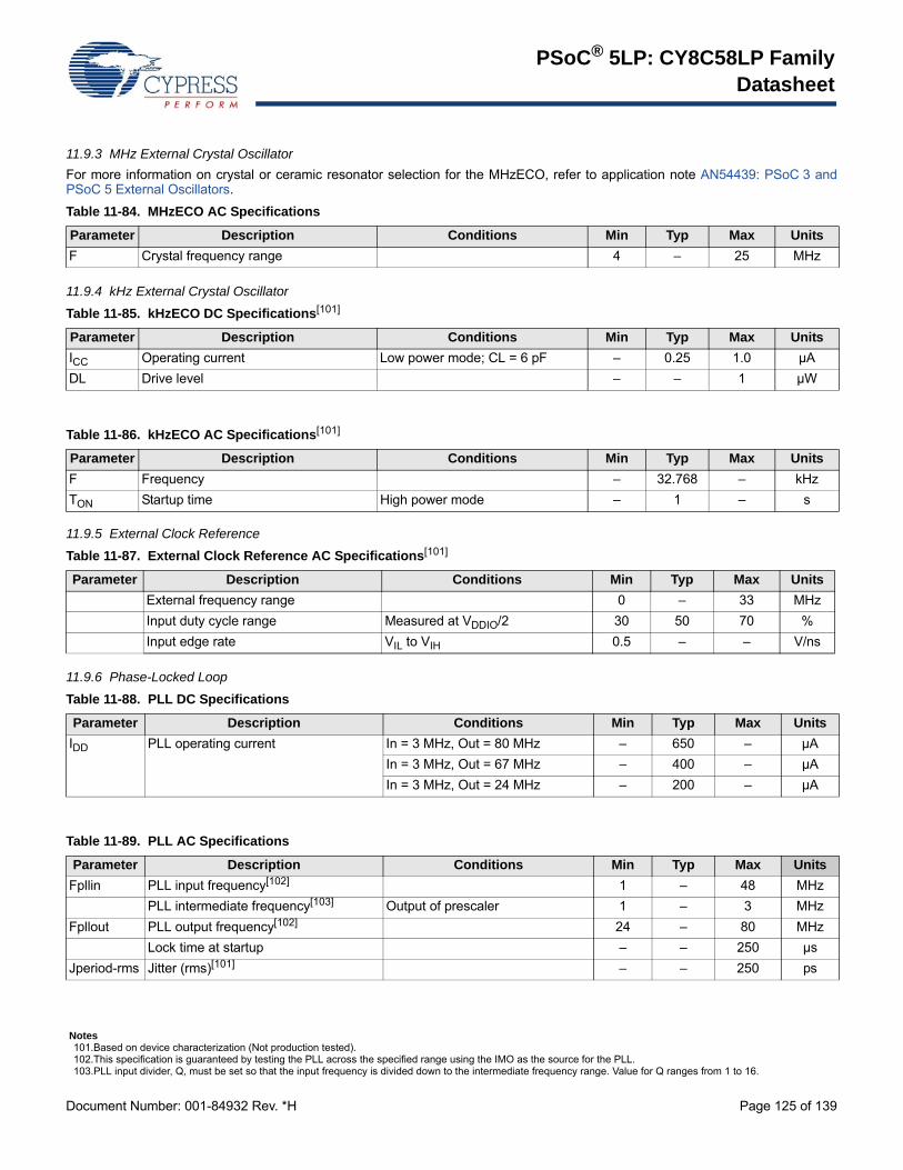
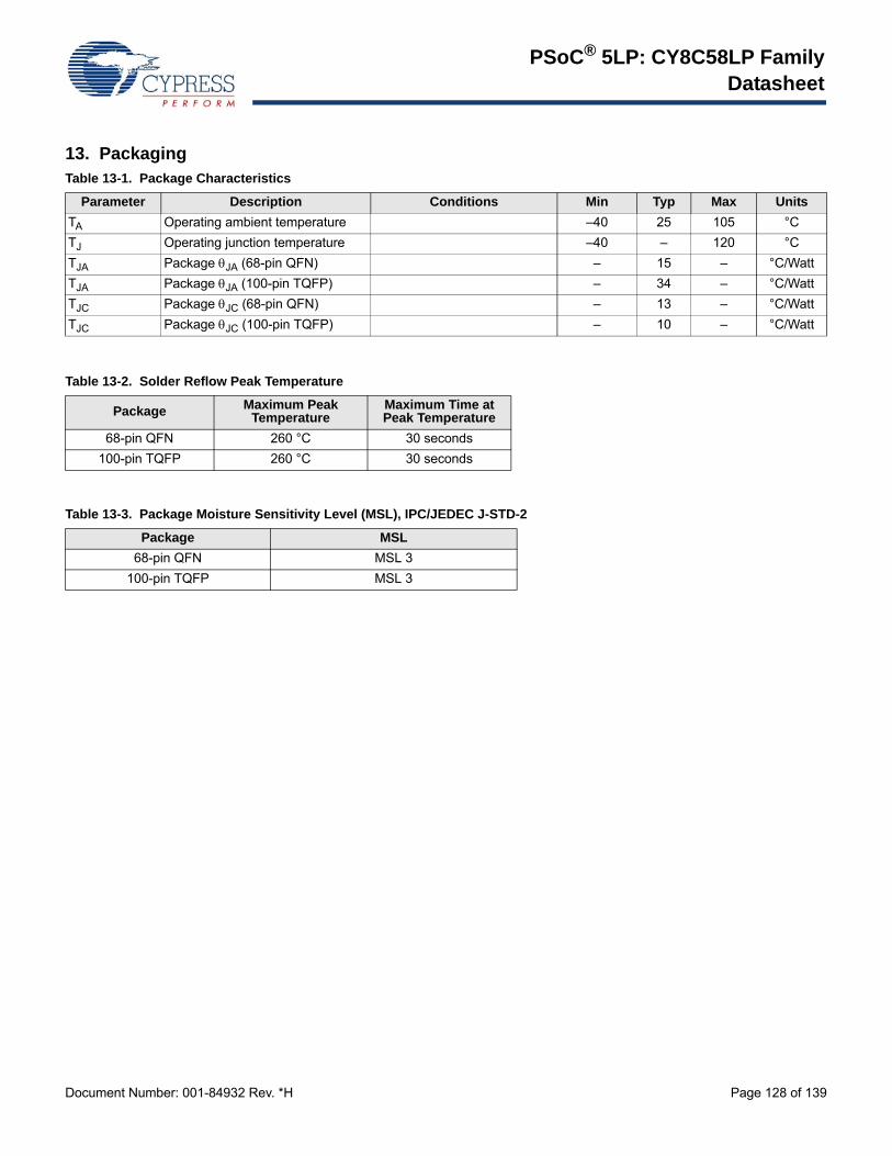
11. Electrical Specifications ........................................... 6511.1 Absolute Maximum Ratings ................................6511.2 Device Level Specifications ................................6611.3 Power Regulators ...............................................7111.4 Inputs and Outputs .............................................7511.5 Analog Peripherals .............................................8411.6 Digital Peripherals ............................................11011.7 Memory ............................................................11511.8 PSoC System Resources .................................11911.9 Clocking ............................................................122
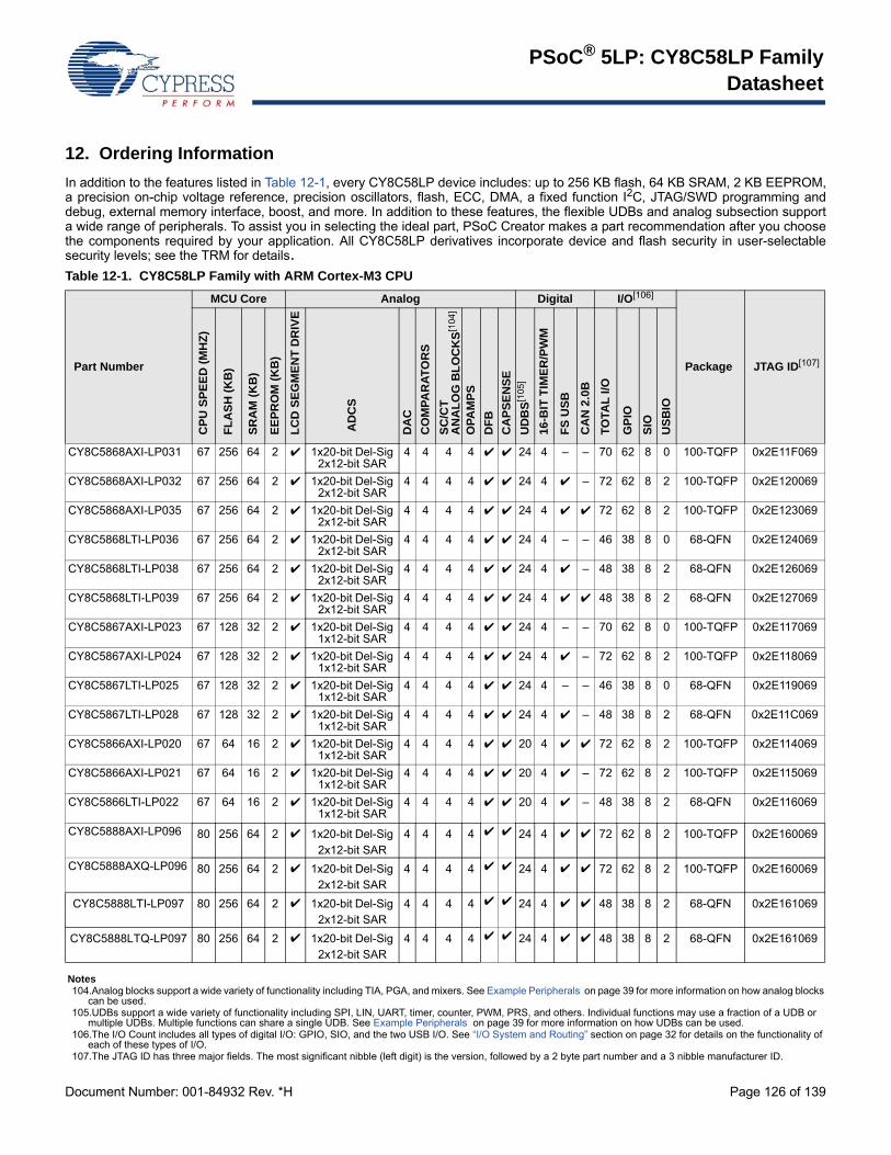
12. Ordering Information ............................................... 12612.1 Part Numbering Conventions ...........................127
Document History Page................................................. 136
Sales, Solutions, and Legal Information ...................... 139Worldwide Sales and Design Support....................... 139Products .................................................................... 139PSoC® Solutions ...................................................... 139Cypress Developer Community................................. 139Technical Support ..................................................... 139
PSoC® 5LP: CY8C58LP FamilyDatasheet
Document Number: 001-84932 Rev. *H Page 4 of 139
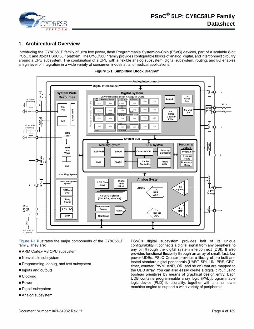
1. Architectural Overview
Introducing the CY8C58LP family of ultra low power, flash Programmable System-on-Chip (PSoC) devices, part of a scalable 8-bitPSoC 3 and 32-bit PSoC 5LP platform. The CY8C58LP family provides configurable blocks of analog, digital, and interconnect circuitryaround a CPU subsystem. The combination of a CPU with a flexible analog subsystem, digital subsystem, routing, and I/O enablesa high level of integration in a wide variety of consumer, industrial, and medical applications.
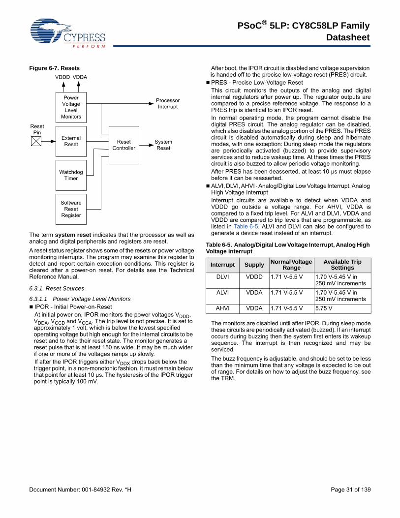
Figure 1-1. Simplified Block Diagram
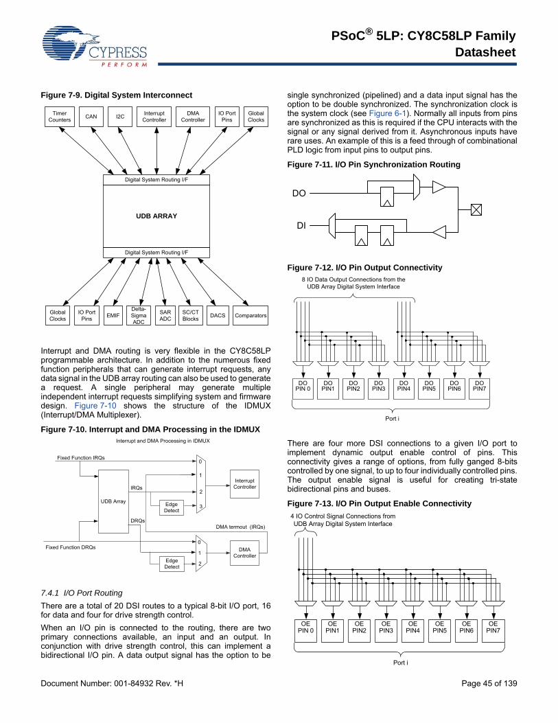
Figure 1-1 illustrates the major components of the CY8C58LPfamily. They are:
ARM Cortex-M3 CPU subsystem
Nonvolatile subsystem
Programming, debug, and test subsystem
Inputs and outputs
Clocking
Power
Digital subsystem
Analog subsystem
PSoC’s digital subsystem provides half of its uniqueconfigurability. It connects a digital signal from any peripheral toany pin through the digital system interconnect (DSI). It alsoprovides functional flexibility through an array of small, fast, lowpower UDBs. PSoC Creator provides a library of pre-built andtested standard digital peripherals (UART, SPI, LIN, PRS, CRC,timer, counter, PWM, AND, OR, and so on) that are mapped tothe UDB array. You can also easily create a digital circuit usingboolean primitives by means of graphical design entry. EachUDB contains programmable array logic (PAL)/programmablelogic device (PLD) functionality, together with a small statemachine engine to support a wide variety of peripherals.
DigitalFilterBlock
LCD Direct Drive
CapSense
Temperature Sensor
4 x Opamp
+
-
ADCs
4 x DAC 1 x Del Sig ADC
4 x SC/ CT Blocks (TIA, PGA, Mixer etc)
4 x CMP
+
-
Program
Debug & Trace
Boundary Scan
Program & Debug
Cortex M3 CPU Interrupt Controller
PHUBDMA
Cache Controller
SRAM
FLASH
EEPROM
EMIF
Digital Interconnect
Analog Interconnect
1.71
to5.
5V
0. 5 to 5.5 V( Optional)
4- 25 MHz( Optional)
XtalOsc
32.768 KHz( Optional)
RTC Timer
IMO Clo
ck T
ree
WDT and
Wake
ILO
Clocking System
1.8 V LDO
SMP
POR andLVD
SleepPower
Power Management System
USB PHY
3 per Opamp
GP
IOs
GP
IOs
GP
IOs
GP
IOs
GP
IOs
GP
IOs
SIO
GP
IOs
SIO
s
2 x SARADC
I2C Master/Slave
Universal Digital Block Array (24 x UDB)
4 xTimer
Counter PWM
FS USB 2.0
UDB
UDB
UDB
UDB
UDB
UDB
UDB UDB UDB
UDB
UDB
UDBUDBUDB UDB
UART
Logic
12- Bit PWM
I 2C Slave8- Bit SPI
12- Bit SPILogic
8- Bit Timer
16- Bit PRS
UDB
8- Bit Timer
Quadrature Decoder 16- Bit PWM
Seq
ue
nc
er
Usa
ge
Exa
mp
le fo
r U
DB UDBUDB
UDBUDB
UDBUDB
UDBUDB
22
Memory System CPU System
Analog System
System Bus
Digital SystemSystem Wide Resources
CAN 2.0
PSoC® 5LP: CY8C58LP FamilyDatasheet
Document Number: 001-84932 Rev. *H Page 5 of 139
In addition to the flexibility of the UDB array, PSoC also providesconfigurable digital blocks targeted at specific functions. For theCY8C58LP family, these blocks can include four 16-bit timers,counters, and PWM blocks; I2C slave, master, and multimaster;Full-Speed USB; and Full CAN 2.0.
For more details on the peripherals see the Example Peripheralson page 39 of this datasheet. For information on UDBs, DSI, andother digital blocks, see the Digital Subsystem on page 39 of thisdatasheet.
PSoC’s analog subsystem is the second half of its uniqueconfigurability. All analog performance is based on a highlyaccurate absolute voltage reference with less than 0.1% errorover temperature and voltage. The configurable analogsubsystem includes:
Analog muxes
Comparators
Analog mixers
Voltage references
ADCs
DACs
Digital filter block (DFB)
All GPIO pins can route analog signals into and out of the deviceusing the internal analog bus. This allows the device to interfaceup to 62 discrete analog signals. One of the ADCs in the analogsubsystem is a fast, accurate, configurable delta-sigma ADCwith these features:
Less than 100-µV offset
A gain error of 0.2%
Integral non linearity (INL) less than ±2 LSB
Differential non linearity (DNL) less than ±1 LSB
SINAD better than 84 dB in 16-bit mode
This converter addresses a wide variety of precision analogapplications including some of the most demanding sensors.
The CY8C58LP family also offers up to two SAR ADCs.Featuring 12-bit conversions at up to 1 M samples per second,they also offer low nonlinearity and offset errors and SNR betterthan 70 dB. They are well-suited for a variety of higher speedanalog applications.
The output of any of the ADCs can optionally feed theprogrammable DFB via DMA without CPU intervention. You canconfigure the DFB to perform IIR and FIR digital filters andseveral user defined custom functions. The DFB can implementfilters with up to 64 taps. It can perform a 48-bitmultiply-accumulate (MAC) operation in one clock cycle.
Four high-speed voltage or current DACs support 8-bit outputsignals at an update rate of up to 8 Msps. They can be routedout of any GPIO pin. You can create higher resolution voltagePWM DAC outputs using the UDB array. This can be used tocreate a pulse width modulated (PWM) DAC of up to 10 bits, atup to 48 kHz. The digital DACs in each UDB support PWM, PRS,or delta-sigma algorithms with programmable widths.
In addition to the ADCs, DACs, and DFB, the analog subsystemprovides multiple:
Comparators
Uncommitted opamps
Configurable switched capacitor/continuous time (SC/CT) blocks. These support: Transimpedance amplifiers Programmable gain amplifiers Mixers Other similar analog components
See the “Analog Subsystem” section on page 50 of thisdatasheet for more details.
PSoC’s CPU subsystem is built around a 32-bit three-stagepipelined ARM Cortex-M3 processor running at up to 80 MHz.The Cortex-M3 includes a tightly integrated nested vectoredinterrupt controller (NVIC) and various debug and trace modules.The overall CPU subsystem includes a DMA controller, flashcache, and RAM. The NVIC provides low latency, nestedinterrupts, and tail-chaining of interrupts and other features toincrease the efficiency of interrupt handling. The DMA controllerenables peripherals to exchange data without CPU involvement.This allows the CPU to run slower (saving power) or use thoseCPU cycles to improve the performance of firmware algorithms.The flash cache also reduces system power consumption byallowing less frequent flash access.
PSoC’s nonvolatile subsystem consists of flash, byte-writeableEEPROM, and nonvolatile configuration options. It provides upto 256 KB of on-chip flash. The CPU can reprogram individualblocks of flash, enabling boot loaders. You can enable an ECCfor high reliability applications. A powerful and flexible protectionmodel secures the user's sensitive information, allowingselective memory block locking for read and write protection.Two KB of byte-writable EEPROM is available on-chip to storeapplication data. Additionally, selected configuration optionssuch as boot speed and pin drive mode are stored in nonvolatilememory. This allows settings to activate immediately after POR.
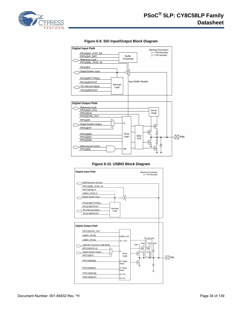
The three types of PSoC I/O are extremely flexible. All I/Os havemany drive modes that are set at POR. PSoC also provides upto four I/O voltage domains through the VDDIO pins. Every GPIOhas analog I/O, LCD drive, CapSense, flexible interruptgeneration, slew rate control, and digital I/O capability. The SIOson PSoC allow VOH to be set independently of VDDIO when usedas outputs. When SIOs are in input mode they are highimpedance. This is true even when the device is not powered orwhen the pin voltage goes above the supply voltage. This makesthe SIO ideally suited for use on an I2C bus where the PSoC maynot be powered when other devices on the bus are. The SIO pinsalso have high current sink capability for applications such asLED drives. The programmable input threshold feature of theSIO can be used to make the SIO function as a general purposeanalog comparator. For devices with FS USB, the USB physicalinterface is also provided (USBIO). When not using USB, thesepins may also be used for limited digital functionality and deviceprogramming. All the features of the PSoC I/Os are covered indetail in the I/O System and Routing on page 32 of thisdatasheet.
PSoC® 5LP: CY8C58LP FamilyDatasheet
Document Number: 001-84932 Rev. *H Page 6 of 139
The PSoC device incorporates flexible internal clock generators,designed for high stability and factory trimmed for high accuracy.The internal main oscillator (IMO) is the master clock base forthe system, and has one-percent accuracy at 3 MHz. The IMOcan be configured to run from 3 MHz up to 74 MHz. Multiple clockderivatives can be generated from the main clock frequency tomeet application needs. The device provides a PLL to generatesystem clock frequencies up to 80 MHz from the IMO, externalcrystal, or external reference clock. It also contains a separate,very low-power internal low-speed oscillator (ILO) for the sleepand watchdog timers. A 32.768-kHz external watch crystal isalso supported for use in RTC applications. The clocks, togetherwith programmable clock dividers, provide the flexibility tointegrate most timing requirements.
The CY8C58LP family supports a wide supply operating rangefrom 1.71 to 5.5 V. This allows operation from regulated suppliessuch as 1.8 ± 5%, 2.5 V ±10%, 3.3 V ± 10%, or 5.0 V ± 10%, ordirectly from a wide range of battery types. In addition, it providesan integrated high efficiency synchronous boost converter thatcan power the device from supply voltages as low as 0.5 V. Thisenables the device to be powered directly from a single battery.In addition, you can use the boost converter to generate othervoltages required by the device, such as a 3.3 V supply for LCDglass drive. The boost’s output is available on the VBOOST pin,allowing other devices in the application to be powered from thePSoC.
PSoC supports a wide range of low power modes. These includea 300-nA hibernate mode with RAM retention and a 2-µA sleepmode with RTC. In the second mode, the optional 32.768-kHzwatch crystal runs continuously and maintains an accurate RTC.
Power to all major functional blocks, including the programmabledigital and analog peripherals, can be controlled independentlyby firmware. This allows low power background processingwhen some peripherals are not in use. This, in turn, provides atotal device current of only 3.1 mA when the CPU is running at6 MHz.
The details of the PSoC power modes are covered in the PowerSystem on page 25 of this datasheet.
PSoC uses JTAG (4 wire) or SWD (2 wire) interfaces forprogramming, debug, and test. Using these standard interfacesyou can debug or program the PSoC with a variety of hardwaresolutions from Cypress or third party vendors. The Cortex-M3debug and trace modules include FPB, DWT, ETM, and ITM.These modules have many features to help solve difficult debugand trace problems. Details of the programming, test, anddebugging interfaces are discussed in the Programming, DebugInterfaces, Resources on page 60 of this datasheet.
2. Pinouts
Each VDDIO pin powers a specific set of I/O pins. (The USBIOsare powered from VDDD.) Using the VDDIO pins, a single PSoCcan support multiple voltage levels, reducing the need foroff-chip level shifters. The black lines drawn on the pinoutdiagrams in Figure 2-3 and Figure 2-4 show the pins that arepowered by each VDDIO.
Each VDDIO may source up to 100 mA total to its associated I/Opins, as shown in Figure 2-1.
Figure 2-1. VDDIO Current Limit
Conversely, for the 100-pin and 68-pin devices, the set of I/Opins associated with any VDDIO may sink up to 100 mA total, asshown in Figure 2-2.
Notes3. The center pad on the QFN package should be connected to digital ground (VSSD) for best mechanical, thermal, and electrical performance. If not connected to
ground, it should be electrically floated and not connected to any other signal. For more information, see AN72845, Design Guidelines for QFN Devices.4. Pins are Do Not Use (DNU) on devices without USB. The pin must be left floating.
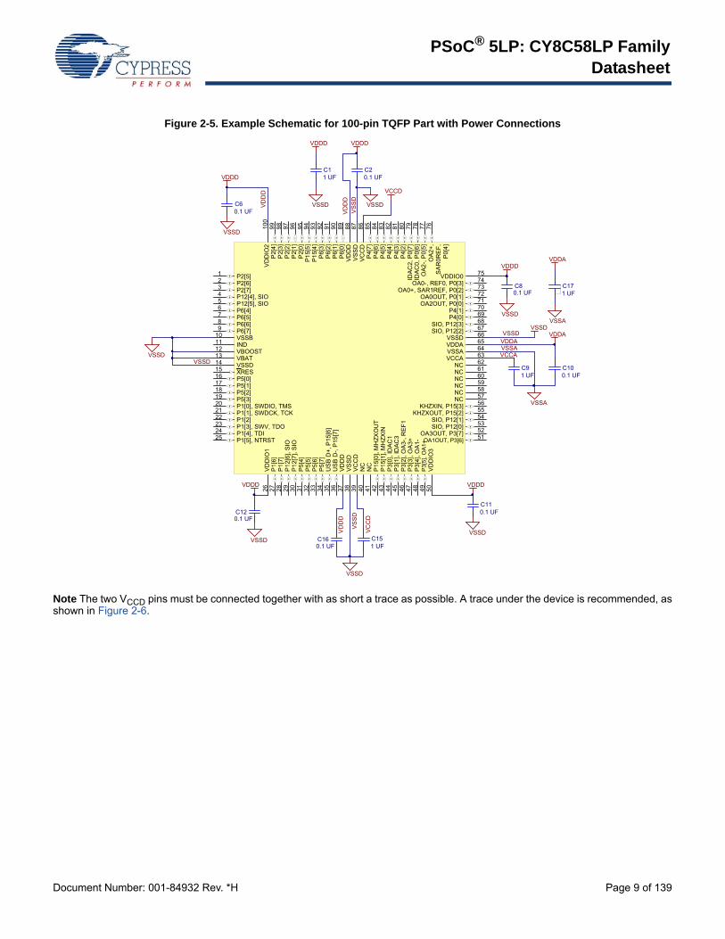
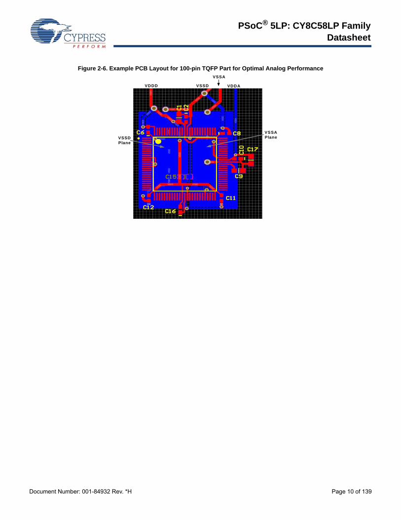
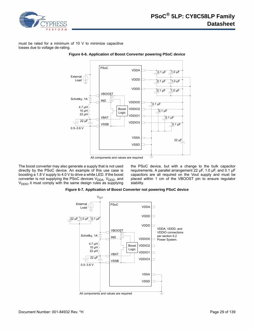
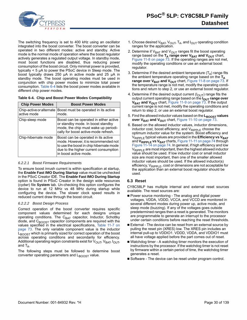
Figure 2-5 on page 9 and Figure 2-6 on page 10 show an example schematic and an example PCB layout, for the 100-pin TQFP part,for optimal analog performance on a two-layer board.
The two pins labeled VDDD must be connected together.
The two pins labeled VCCD must be connected together, with capacitance added, as shown in Figure 2-5 and Power System on page 25. The trace between the two VCCD pins should be as short as possible.
The two pins labeled VSSD must be connected together.
For information on circuit board layout issues for mixed signals, refer to the application note, AN57821 - Mixed Signal Circuit BoardLayout Considerations for PSoC® 3 and PSoC 5.
Opamp0+, Opamp1+, Opamp2+, Opamp3+. Noninvertinginput to uncommitted opamp.
GPIO. Provides interfaces to the CPU, digital peripherals,analog peripherals, interrupts, LCD segment drive, andCapSense.[6]
I2C0: SCL, I2C1: SCL. I2C SCL line providing wake from sleepon an address match. Any I/O pin can be used for I2C SCL ifwake from sleep is not required.
I2C0: SDA, I2C1: SDA. I2C SDA line providing wake from sleepon an address match. Any I/O pin can be used for I2C SDA ifwake from sleep is not required.
Ind. Inductor connection to boost pump.
kHz XTAL: Xo, kHz XTAL: Xi. 32.768-kHz crystal oscillator pin.
MHz XTAL: Xo, MHz XTAL: Xi. 4 to 25-MHz crystal oscillatorpin.
nTRST. Optional JTAG Test Reset programming and debug portconnection to reset the JTAG connection.
SIO. Provides interfaces to the CPU, digital peripherals andinterrupts with a programmable high threshold voltage, analogcomparator, high sink current, and high impedance state whenthe device is unpowered.
SWDCK. SWD Clock programming and debug port connection.
SWDIO. SWD Input and Output programming and debug portconnection.
TCK. JTAG Test Clock programming and debug port connection.
TDI. JTAG Test Data In programming and debug portconnection.
TDO. JTAG Test Data Out programming and debug portconnection.
TMS. JTAG Test Mode Select programming and debug portconnection.
USBIO, D+. Provides D+ connection directly to a USB 2.0 bus.May be used as a digital I/O pin; it is powered from VDDD insteadof from a VDDIO. Pins are Do Not Use (DNU) on devices withoutUSB.
USBIO, D-. Provides D- connection directly to a USB 2.0 bus.May be used as a digital I/O pin; it is powered from VDDD insteadof from a VDDIO. Pins are Do Not Use (DNU) on devices withoutUSB.
VBOOST. Power sense connection to boost pump.
VBAT. Battery supply to boost pump.
VCCA. Output of the analog core regulator or the input tothe analog core. Requires a 1uF capacitor to VSSA. Theregulator output is not designed to drive external circuits. Notethat if you use the device with an external core regulator(externally regulated mode), the voltage applied to this pinmust not exceed the allowable range of 1.71 V to 1.89 V.When using the internal core regulator, (internally regulatedmode, the default), do not tie any power to this pin. For detailssee Power System on page 25.
VCCD. Output of the digital core regulator or the input to thedigital core. The two VCCD pins must be shorted together, withthe trace between them as short as possible, and a 1uF capacitorto VSSD. The regulator output is not designed to drive externalcircuits. Note that if you use the device with an external coreregulator (externally regulated mode), the voltage applied tothis pin must not exceed the allowable range of 1.71 V to1.89 V. When using the internal core regulator (internallyregulated mode, the default), do not tie any power to this pin. Fordetails see Power System on page 25.
VDDA. Supply for all analog peripherals and analog coreregulator. VDDA must be the highest voltage present on thedevice. All other supply pins must be less than or equal toVDDA.
VDDD. Supply for all digital peripherals and digital coreregulator. VDDD must be less than or equal to VDDA.
VSSA. Ground for all analog peripherals.
VSSB. Ground connection for boost pump.
VSSD. Ground for all digital logic and I/O pins.
VDDIO0, VDDIO1, VDDIO2, VDDIO3. Supply for I/O pins. EachVDDIO must be tied to a valid operating voltage (1.71 V to 5.5 V),and must be less than or equal to VDDA.
XRES (and configurable XRES). External reset pin. Active lowwith internal pull-up. Pin P1[2] may be configured to be a XRESpin; see “Nonvolatile Latches (NVLs)” on page 19.
Note6. GPIOs with opamp outputs are not recommended for use with CapSense.
PSoC® 5LP: CY8C58LP FamilyDatasheet
Document Number: 001-84932 Rev. *H Page 12 of 139
4. CPU
4.1 ARM Cortex-M3 CPU
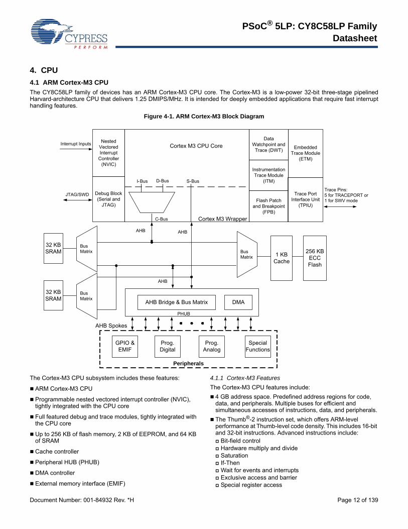
The CY8C58LP family of devices has an ARM Cortex-M3 CPU core. The Cortex-M3 is a low-power 32-bit three-stage pipelinedHarvard-architecture CPU that delivers 1.25 DMIPS/MHz. It is intended for deeply embedded applications that require fast interrupthandling features.
Figure 4-1. ARM Cortex-M3 Block Diagram
The Cortex-M3 CPU subsystem includes these features:
ARM Cortex-M3 CPU
Programmable nested vectored interrupt controller (NVIC), tightly integrated with the CPU core
Full featured debug and trace modules, tightly integrated with the CPU core
Up to 256 KB of flash memory, 2 KB of EEPROM, and 64 KB of SRAM
Cache controller
Peripheral HUB (PHUB)
DMA controller
External memory interface (EMIF)
4.1.1 Cortex-M3 Features
The Cortex-M3 CPU features include:
4 GB address space. Predefined address regions for code, data, and peripherals. Multiple buses for efficient and simultaneous accesses of instructions, data, and peripherals.
The Thumb®-2 instruction set, which offers ARM-level performance at Thumb-level code density. This includes 16-bit and 32-bit instructions. Advanced instructions include: Bit-field control Hardware multiply and divide Saturation If-Then Wait for events and interrupts Exclusive access and barrier Special register access
Nested Vectored Interrupt
Controller (NVIC)
Debug Block (Serial and
JTAG)
Embedded Trace Module
(ETM)
Trace Port Interface Unit
(TPIU)
Interrupt Inputs
JTAG/SWDTrace Pins:5 for TRACEPORT or1 for SWV mode
Cortex M3 CPU Core
I-Bus S-BusD-Bus
256 KB ECC Flash
1 KB Cache
32 KB SRAM
DMA AHB Bridge & Bus Matrix
PHUB
GPIO & EMIF
Prog. Digital
Prog. Analog
Special Functions
Peripherals
AHB Spokes
AHB AHB
AHB
Bus Matrix
Cortex M3 WrapperC-Bus
Data Watchpoint and
Trace (DWT)
Instrumentation Trace Module
(ITM)
Flash Patch and Breakpoint
(FPB)
Bus Matrix
32 KB SRAM
Bus Matrix
PSoC® 5LP: CY8C58LP FamilyDatasheet
Document Number: 001-84932 Rev. *H Page 13 of 139
The Cortex-M3 does not support ARM instructions for SRAMaddresses.
Bit-band support for the SRAM region. Atomic bit-level write and read operations for SRAM addresses.
Unaligned data storage and access. Contiguous storage of data of different byte lengths.
Operation at two privilege levels (privileged and user) and in two modes (thread and handler). Some instructions can only be executed at the privileged level. There are also two stack pointers: Main (MSP) and Process (PSP). These features support a multitasking operating system running one or more user-level processes.
Extensive interrupt and system exception support.
4.1.2 Cortex-M3 Operating Modes
The Cortex-M3 operates at either the privileged level or the userlevel, and in either the thread mode or the handler mode.Because the handler mode is only enabled at the privileged level,there are actually only three states, as shown in Table 4-1.
At the user level, access to certain instructions, special registers,configuration registers, and debugging components is blocked.Attempts to access them cause a fault exception. At theprivileged level, access to all instructions and registers isallowed.
The processor runs in the handler mode (always at the privilegedlevel) when handling an exception, and in the thread mode whennot.
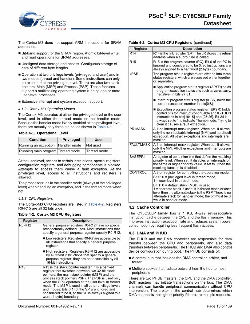
4.1.3 CPU Registers
The Cortex-M3 CPU registers are listed in Table 4-2. RegistersR0-R15 are all 32 bits wide. 4.2 Cache Controller
The CY8C58LP family has a 1 KB, 4-way set-associativeinstruction cache between the CPU and the flash memory. Thisimproves instruction execution rate and reduces system powerconsumption by requiring less frequent flash access.
4.3 DMA and PHUB
The PHUB and the DMA controller are responsible for datatransfer between the CPU and peripherals, and also datatransfers between peripherals. The PHUB and DMA also controldevice configuration during boot. The PHUB consists of:
A central hub that includes the DMA controller, arbiter, and router
Multiple spokes that radiate outward from the hub to most peripherals
There are two PHUB masters: the CPU and the DMA controller.Both masters may initiate transactions on the bus. The DMAchannels can handle peripheral communication without CPUintervention. The arbiter in the central hub determines whichDMA channel is the highest priority if there are multiple requests.
Table 4-1. Operational Level
Condition Privileged User
Running an exception Handler mode Not used
Running main program Thread mode Thread mode
Table 4-2. Cortex M3 CPU Registers
Register DescriptionR0-R12 General purpose registers R0-R12 have no special
architecturally defined uses. Most instructions that specify a general purpose register specify R0-R12.
Low registers: Registers R0-R7 are accessible by all instructions that specify a general purpose register.
High registers: Registers R8-R12 are accessible by all 32-bit instructions that specify a general purpose register; they are not accessible by all 16-bit instructions.
R13 R13 is the stack pointer register. It is a banked register that switches between two 32-bit stack pointers: the main stack pointer (MSP) and the process stack pointer (PSP). The PSP is used only when the CPU operates at the user level in thread mode. The MSP is used in all other privilege levels and modes. Bits[0:1] of the SP are ignored and considered to be 0, so the SP is always aligned to a word (4 byte) boundary.
R14 R14 is the link register (LR). The LR stores the return address when a subroutine is called.
R15 R15 is the program counter (PC). Bit 0 of the PC is ignored and considered to be 0, so instructions are always aligned to a half word (2 byte) boundary.
xPSR The program status registers are divided into three status registers, which are accessed either together or separately:
Application program status register (APSR) holds program execution status bits such as zero, carry, negative, in bits[27:31].
Interrupt program status register (IPSR) holds the current exception number in bits[0:8].
Execution program status register (EPSR) holds control bits for interrupt continuable and IF-THEN instructions in bits[10:15] and [25:26]. Bit 24 is always set to 1 to indicate Thumb mode. Trying to clear it causes a fault exception.
PRIMASK A 1-bit interrupt mask register. When set, it allows only the nonmaskable interrupt (NMI) and hard fault exception. All other exceptions and interrupts are masked.
FAULTMASK A 1-bit interrupt mask register. When set, it allows only the NMI. All other exceptions and interrupts are masked.
BASEPRI A register of up to nine bits that define the masking priority level. When set, it disables all interrupts of the same or higher priority value. If set to 0 then the masking function is disabled.
CONTROL A 2-bit register for controlling the operating mode.Bit 0: 0 = privileged level in thread mode, 1 = user level in thread mode.Bit 1: 0 = default stack (MSP) is used, 1 = alternate stack is used. If in thread mode or user level then the alternate stack is the PSP. There is no alternate stack for handler mode; the bit must be 0 while in handler mode.
Table 4-2. Cortex M3 CPU Registers (continued)
Register Description
PSoC® 5LP: CY8C58LP FamilyDatasheet
Document Number: 001-84932 Rev. *H Page 14 of 139
4.3.1 PHUB Features
CPU and DMA controller are both bus masters to the PHUB
Eight multi-layer AHB bus parallel access paths (spokes) for peripheral access
Simultaneous CPU and DMA access to peripherals located on different spokes
Simultaneous DMA source and destination burst transactions on different spokes
Supports 8-, 16-, 24-, and 32-bit addressing and data
4.3.2 DMA Features
24 DMA channels
Each channel has one or more transaction descriptors (TDs) to configure channel behavior. Up to 128 total TDs can be defined
TDs can be dynamically updated
Eight levels of priority per channel
Any digitally routable signal, the CPU, or another DMA channel, can trigger a transaction
Each channel can generate up to two interrupts per transfer
Transactions can be stalled or canceled
Supports transaction size of infinite or 1 to 64k bytes
Large transactions may be broken into smaller bursts of 1 to 127 bytes
TDs may be nested and/or chained for complex transactions
4.3.3 Priority Levels
The CPU always has higher priority than the DMA controllerwhen their accesses require the same bus resources. Due to thesystem architecture, the CPU can never starve the DMA. DMAchannels of higher priority (lower priority number) may interruptcurrent DMA transfers. In the case of an interrupt, the currenttransfer is allowed to complete its current transaction. To ensurelatency limits when multiple DMA accesses are requestedsimultaneously, a fairness algorithm guarantees an interleavedminimum percentage of bus bandwidth for priority levels 2through 7. Priority levels 0 and 1 do not take part in the fairnessalgorithm and may use 100% of the bus bandwidth. If a tie occurson two DMA requests of the same priority level, a simple roundrobin method is used to evenly share the allocated bandwidth.The round robin allocation can be disabled for each DMAchannel, allowing it to always be at the head of the line. Prioritylevels 2 to 7 are guaranteed the minimum bus bandwidth shownin Table 4-4 after the CPU and DMA priority levels 0 and 1 havesatisfied their requirements.
When the fairness algorithm is disabled, DMA access is grantedbased solely on the priority level; no bus bandwidth guaranteesare made.
4.3.4 Transaction Modes Supported
The flexible configuration of each DMA channel and the ability tochain multiple channels allow the creation of both simple andcomplex use cases. General use cases include, but are notlimited to:
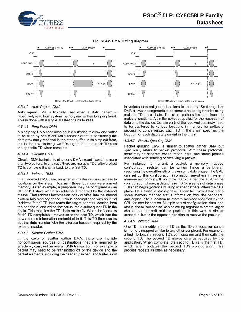
4.3.4.1 Simple DMA
In a simple DMA case, a single TD transfers data between asource and sink (peripherals or memory location). The basictiming diagrams of DMA read and write cycles are shown inFigure 4-2. For more description on other transfer modes, referto the Technical Reference Manual.
Table 4-3. PHUB Spokes and Peripherals
PHUB Spokes Peripherals
0 SRAM
1 IOs, PICU, EMIF
2 PHUB local configuration, Power manager, Clocks, IC, SWV, EEPROM, Flash programming interface
3 Analog interface and trim, Decimator
4 USB, CAN, I2C, Timers, Counters, and PWMs
5 DFB
6 UDBs group 1
7 UDBs group 2
Table 4-4. Priority Levels
Priority Level % Bus Bandwidth
0 100.0
1 100.0
2 50.0
3 25.0
4 12.5
5 6.2
6 3.1
7 1.5
PSoC® 5LP: CY8C58LP FamilyDatasheet
Document Number: 001-84932 Rev. *H Page 15 of 139
Figure 4-2. DMA Timing Diagram
4.3.4.2 Auto Repeat DMA
Auto repeat DMA is typically used when a static pattern isrepetitively read from system memory and written to a peripheral.This is done with a single TD that chains to itself.
4.3.4.3 Ping Pong DMA
A ping pong DMA case uses double buffering to allow one bufferto be filled by one client while another client is consuming thedata previously received in the other buffer. In its simplest form,this is done by chaining two TDs together so that each TD callsthe opposite TD when complete.
4.3.4.4 Circular DMA
Circular DMA is similar to ping pong DMA except it contains morethan two buffers. In this case there are multiple TDs; after the lastTD is complete it chains back to the first TD.
4.3.4.5 Indexed DMA
In an indexed DMA case, an external master requires access tolocations on the system bus as if those locations were sharedmemory. As an example, a peripheral may be configured as anSPI or I2C slave where an address is received by the externalmaster. That address becomes an index or offset into the internalsystem bus memory space. This is accomplished with an initial“address fetch” TD that reads the target address location fromthe peripheral and writes that value into a subsequent TD in thechain. This modifies the TD chain on the fly. When the “addressfetch” TD completes it moves on to the next TD, which has thenew address information embedded in it. This TD then carriesout the data transfer with the address location required by theexternal master.
4.3.4.6 Scatter Gather DMA
In the case of scatter gather DMA, there are multiplenoncontiguous sources or destinations that are required toeffectively carry out an overall DMA transaction. For example, apacket may need to be transmitted off of the device and thepacket elements, including the header, payload, and trailer, exist
in various noncontiguous locations in memory. Scatter gatherDMA allows the segments to be concatenated together by usingmultiple TDs in a chain. The chain gathers the data from themultiple locations. A similar concept applies for the reception ofdata onto the device. Certain parts of the received data may needto be scattered to various locations in memory for softwareprocessing convenience. Each TD in the chain specifies thelocation for each discrete element in the chain.
4.3.4.7 Packet Queuing DMA
Packet queuing DMA is similar to scatter gather DMA butspecifically refers to packet protocols. With these protocols,there may be separate configuration, data, and status phasesassociated with sending or receiving a packet.
For instance, to transmit a packet, a memory mappedconfiguration register can be written inside a peripheral,specifying the overall length of the ensuing data phase. The CPUcan set up this configuration information anywhere in systemmemory and copy it with a simple TD to the peripheral. After theconfiguration phase, a data phase TD (or a series of data phaseTDs) can begin (potentially using scatter gather). When the dataphase TD(s) finish, a status phase TD can be invoked that readssome memory mapped status information from the peripheraland copies it to a location in system memory specified by theCPU for later inspection. Multiple sets of configuration, data, andstatus phase “subchains” can be strung together to create largerchains that transmit multiple packets in this way. A similarconcept exists in the opposite direction to receive the packets.
4.3.4.8 Nested DMA
One TD may modify another TD, as the TD configuration spaceis memory mapped similar to any other peripheral. For example,a first TD loads a second TD’s configuration and then calls thesecond TD. The second TD moves data as required by theapplication. When complete, the second TD calls the first TD,which again updates the second TD’s configuration. Thisprocess repeats as often as necessary.
CLK
ADDR 16/32
WRITE
DATA
READY
Basic DMA Read Transfer without wait states
A B
DATA (A)
ADDRESS Phase DATA Phase
A B
ADDRESS Phase DATA Phase
CLK
WRITE
DATA
READY
DATA (A)
Basic DMA Write Transfer without wait states
ADDR 16/32
PSoC® 5LP: CY8C58LP FamilyDatasheet
Document Number: 001-84932 Rev. *H Page 16 of 139
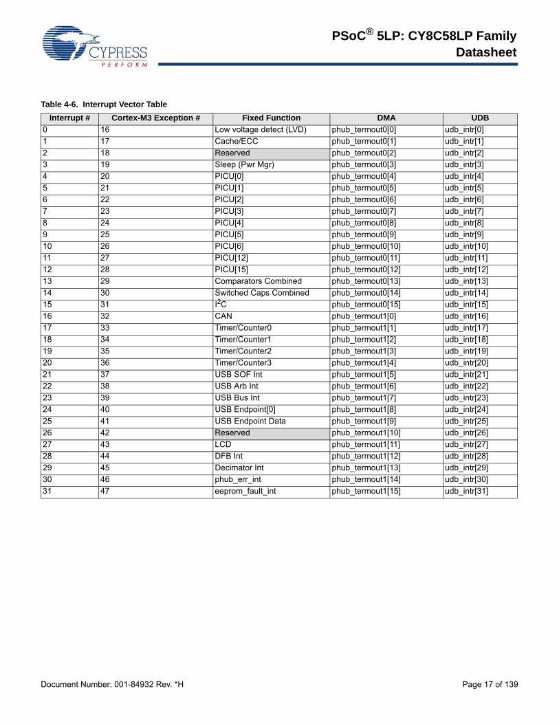
4.4 Interrupt Controller
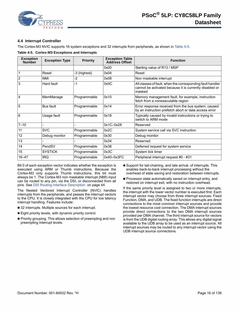
The Cortex-M3 NVIC supports 16 system exceptions and 32 interrupts from peripherals, as shown in Table 4-5.
Bit 0 of each exception vector indicates whether the exception isexecuted using ARM or Thumb instructions. Because theCortex-M3 only supports Thumb instructions, this bit mustalways be 1. The Cortex-M3 non maskable interrupt (NMI) inputcan be routed to any pin, via the DSI, or disconnected from allpins. See DSI Routing Interface Description on page 44.
The Nested Vectored Interrupt Controller (NVIC) handlesinterrupts from the peripherals, and passes the interrupt vectorsto the CPU. It is closely integrated with the CPU for low latencyinterrupt handling. Features include:
32 interrupts. Multiple sources for each interrupt.
Eight priority levels, with dynamic priority control.
Priority grouping. This allows selection of preempting and non preempting interrupt levels.
Support for tail-chaining, and late arrival, of interrupts. This enables back-to-back interrupt processing without the overhead of state saving and restoration between interrupts.
Processor state automatically saved on interrupt entry, and restored on interrupt exit, with no instruction overhead.
If the same priority level is assigned to two or more interrupts,the interrupt with the lower vector number is executed first. Eachinterrupt vector may choose from three interrupt sources: FixedFunction, DMA, and UDB. The fixed function interrupts are directconnections to the most common interrupt sources and providethe lowest resource cost connection. The DMA interrupt sourcesprovide direct connections to the two DMA interrupt sourcesprovided per DMA channel. The third interrupt source for vectorsis from the UDB digital routing array. This allows any digital signalavailable to the UDB array to be used as an interrupt source. Allinterrupt sources may be routed to any interrupt vector using theUDB interrupt source connections.
Table 4-5. Cortex-M3 Exceptions and Interrupts
Exception Number Exception Type Priority Exception Table
Address Offset Function
0x00 Starting value of R13 / MSP
1 Reset -3 (highest) 0x04 Reset
2 NMI -2 0x08 Non maskable interrupt
3 Hard fault -1 0x0C All classes of fault, when the corresponding fault handler cannot be activated because it is currently disabled or masked
4 MemManage Programmable 0x10 Memory management fault, for example, instruction fetch from a nonexecutable region
5 Bus fault Programmable 0x14 Error response received from the bus system; caused by an instruction prefetch abort or data access error
6 Usage fault Programmable 0x18 Typically caused by invalid instructions or trying to switch to ARM mode
7–10 - - 0x1C–0x28 Reserved
11 SVC Programmable 0x2C System service call via SVC instruction
12 Debug monitor Programmable 0x30 Debug monitor
13 - - 0x34 Reserved
14 PendSV Programmable 0x38 Deferred request for system service
CY8C58LP static RAM (SRAM) is used for temporary datastorage. Code can be executed at full speed from the portion ofSRAM that is located in the code space. This process is slowerfrom SRAM above 0x20000000. The device provides up to 64KB of SRAM. The CPU or the DMA controller can access all ofSRAM. The SRAM can be accessed simultaneously by theCortex-M3 CPU and the DMA controller if accessing different32-KB blocks.
5.2 Flash Program Memory
Flash memory in PSoC devices provides nonvolatile storage foruser firmware, user configuration data, bulk data storage, andoptional ECC data. The main flash memory area contains up to256 KB of user program space.
Up to an additional 32 KB of flash space is available for ErrorCorrecting Codes (ECC). If ECC is not used this space can storedevice configuration data and bulk user data. User code may notbe run out of the ECC flash memory section. ECC can correctone bit error and detect two bit errors per 8 bytes of firmwarememory; an interrupt can be generated when an error isdetected. The flash output is 9 bytes wide with 8 bytes of dataand 1 byte of ECC data.
The CPU or DMA controller read both user code and bulk datalocated in flash through the cache controller. This provideshigher CPU performance. If ECC is enabled, the cache controlleralso performs error checking and correction.
Flash programming is performed through a special interface andpreempts code execution out of flash. Code execution may bedone out of SRAM during flash programming.
The flash 24programming interface performs flash erasing,programming and setting code protection levels. Flash in-systemserial programming (ISSP), typically used for productionprogramming, is possible through both the SWD and JTAGinterfaces. In-system programming, typically used forbootloaders, is also possible using serial interfaces such as I2C,USB, UART, and SPI, or any communications protocol.
5.3 Flash Security
All PSoC devices include a flexible flash protection model thatprevents access and visibility to on-chip flash memory. Thisprevents duplication or reverse engineering of proprietary code.Flash memory is organized in blocks, where each block contains256 bytes of program or data and 32 bytes of ECC orconfiguration data.
The device offers the ability to assign one of four protectionlevels to each row of flash. Table 5-1 lists the protection modesavailable. Flash protection levels can only be changed byperforming a complete flash erase. The Full Protection and FieldUpgrade settings disable external access (through a debuggingtool such as PSoC Creator, for example). If your applicationrequires code update through a boot loader, then use the FieldUpgrade setting. Use the Unprotected setting only when nosecurity is needed in your application. The PSoC device alsooffers an advanced security feature called Device Security whichpermanently disables all test, programming, and debug ports,protecting your application from external access (see the
“Device Security” section on page 63). For more information onhow to take full advantage of the security features in PSoC, seethe PSoC 5 TRM.
Disclaimer
Note the following details of the flash code protection features onCypress devices.
Cypress products meet the specifications contained in theirparticular Cypress datasheets. Cypress believes that its family ofproducts is one of the most secure families of its kind on themarket today, regardless of how they are used. There may bemethods, unknown to Cypress, that can breach the codeprotection features. Any of these methods, to our knowledge,would be dishonest and possibly illegal. Neither Cypress nor anyother semiconductor manufacturer can guarantee the security oftheir code. Code protection does not mean that we areguaranteeing the product as “unbreakable.”
Cypress is willing to work with the customer who is concernedabout the integrity of their code. Code protection is constantlyevolving. We at Cypress are committed to continuouslyimproving the code protection features of our products.
5.4 EEPROM
PSoC EEPROM memory is a byte addressable nonvolatilememory. The CY8C58LP has 2 KB of EEPROM memory to storeuser data. Reads from EEPROM are random access at the bytelevel. Reads are done directly; writes are done by sending writecommands to an EEPROM programming interface. CPU codeexecution can continue from flash during EEPROM writes.EEPROM is erasable and writeable at the row level. TheEEPROM is divided into 128 rows of 16 bytes each. The factorydefault values of all EEPROM bytes are 0.
Because the EEPROM is mapped to the Cortex-M3 Peripheralregion, the CPU cannot execute out of EEPROM. There is noECC hardware associated with EEPROM. If ECC is required itmust be handled in firmware.
It can take as much as 20 milliseconds to write to EEPROM orflash. During this time the device should not be reset, orunexpected changes may be made to portions of EEPROM orflash. Reset sources (see Reset Sources on page 31) includeXRES pin, software reset, and watchdog; care should be takento make sure that these are not inadvertently activated. Inaddition, the low voltage detect circuits should be configured togenerate an interrupt instead of a reset.
Table 5-1. Flash Protection
ProtectionSetting Allowed Not Allowed
Unprotected External read and write + internal read and write
–
Factory Upgrade
External write + internal read and write
External read
Field Upgrade Internal read and write External read and write
Full Protection Internal read External read and write + internal write
PSoC® 5LP: CY8C58LP FamilyDatasheet
Document Number: 001-84932 Rev. *H Page 19 of 139
5.5 Nonvolatile Latches (NVLs)
PSoC has a 4-byte array of nonvolatile latches (NVLs) that are used to configure the device at reset. The NVL register map is shownin Table 5-3.
The details for individual fields and their factory default settings are shown in Table 5-3:.
Although PSoC Creator provides support for modifying the device configuration NVLs, the number of NVL erase/write cycles is limited– see “Nonvolatile Latches (NVL)” on page 116.
PRTxRDM[1:0] Controls reset drive mode of the corresponding IO port. See “Reset Configuration” on page 38. All pins of the port are set to the same mode.
00b (default) - high impedance analog01b - high impedance digital10b - resistive pull up11b - resistive pull down
XRESMEN Controls whether pin P1[2] is used as a GPIO or as an external reset. See “Pin Descriptions” on page 11, XRES description.
0 (default) - GPIO1 - external reset
DBGEN Debug Enable allows access to the debug system, for third-party programmers.
0 - access disabled1 (default) - access enabled
CFGSPEED Controls the speed of the IMO-based clock during the device boot process, for faster boot or low-power operation
0 (default) - 12 MHz IMO1 - 48 MHz IMO
DPS[1:0] Controls the usage of various P1 pins as a debug port. See “Programming, Debug Interfaces, Resources” on page 60.
ECCEN Controls whether ECC flash is used for ECC or for general configuration and data storage. See “Flash Program Memory” on page 18.
0 - ECC disabled1 (default) - ECC enabled
DIG_PHS_DLY[3:0] Selects the digital clock phase delay. See the TRM for details.
PSoC® 5LP: CY8C58LP FamilyDatasheet
Document Number: 001-84932 Rev. *H Page 20 of 139
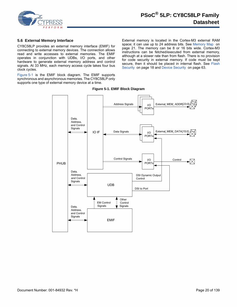
5.6 External Memory Interface
CY8C58LP provides an external memory interface (EMIF) forconnecting to external memory devices. The connection allowsread and write accesses to external memories. The EMIFoperates in conjunction with UDBs, I/O ports, and otherhardware to generate external memory address and controlsignals. At 33 MHz, each memory access cycle takes four busclock cycles.
Figure 5-1 is the EMIF block diagram. The EMIF supportssynchronous and asynchronous memories. The CY8C58LP onlysupports one type of external memory device at a time.
External memory is located in the Cortex-M3 external RAMspace; it can use up to 24 address bits. See Memory Map onpage 21. The memory can be 8 or 16 bits wide. Cortex-M3instructions can be fetched/executed from external memory,although at a slower rate than from flash. There is no provisionfor code security in external memory. If code must be keptsecure, then it should be placed in internal flash. See FlashSecurity on page 18 and Device Security on page 63.
Figure 5-1. EMIF Block Diagram
PHUB
IO IF
UDB
EMIF
I/O PORTs
I/O PORTs
I/O PORTs
Data, Address, and Control Signals
Data, Address, and Control Signals
Address Signals
Data Signals
Control Signals
Data, Address, and Control Signals
EM Control Signals
Other Control Signals
DSI Dynamic Output Control
DSI to Port
Control
External_MEM_ DATA[15:0]
External_MEM_ ADDR[23:0]
PSoC® 5LP: CY8C58LP FamilyDatasheet
Document Number: 001-84932 Rev. *H Page 21 of 139
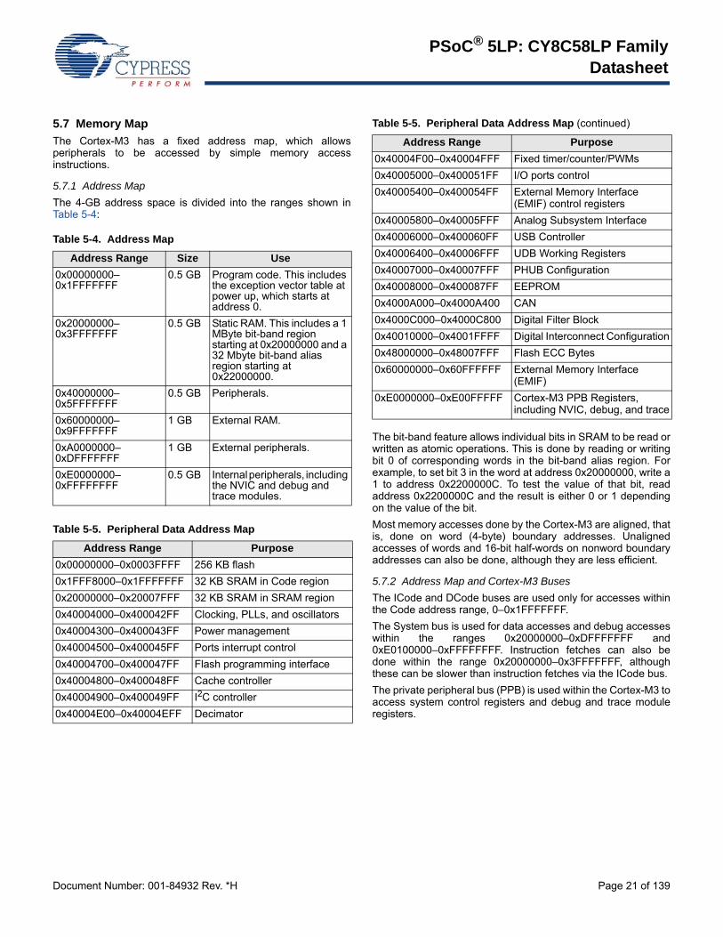
5.7 Memory Map
The Cortex-M3 has a fixed address map, which allowsperipherals to be accessed by simple memory accessinstructions.
5.7.1 Address Map
The 4-GB address space is divided into the ranges shown inTable 5-4:
The bit-band feature allows individual bits in SRAM to be read orwritten as atomic operations. This is done by reading or writingbit 0 of corresponding words in the bit-band alias region. Forexample, to set bit 3 in the word at address 0x20000000, write a1 to address 0x2200000C. To test the value of that bit, readaddress 0x2200000C and the result is either 0 or 1 dependingon the value of the bit.
Most memory accesses done by the Cortex-M3 are aligned, thatis, done on word (4-byte) boundary addresses. Unalignedaccesses of words and 16-bit half-words on nonword boundaryaddresses can also be done, although they are less efficient.
5.7.2 Address Map and Cortex-M3 Buses
The ICode and DCode buses are used only for accesses withinthe Code address range, 0–0x1FFFFFFF.
The System bus is used for data accesses and debug accesseswithin the ranges 0x20000000–0xDFFFFFFF and0xE0100000–0xFFFFFFFF. Instruction fetches can also bedone within the range 0x20000000–0x3FFFFFFF, althoughthese can be slower than instruction fetches via the ICode bus.
The private peripheral bus (PPB) is used within the Cortex-M3 toaccess system control registers and debug and trace moduleregisters.
Table 5-4. Address Map
Address Range Size Use
0x00000000–0x1FFFFFFF
0.5 GB Program code. This includes the exception vector table at power up, which starts at address 0.
0x20000000–0x3FFFFFFF
0.5 GB Static RAM. This includes a 1 MByte bit-band region starting at 0x20000000 and a 32 Mbyte bit-band alias region starting at 0x22000000.
0x40000000–0x5FFFFFFF
0.5 GB Peripherals.
0x60000000–0x9FFFFFFF
1 GB External RAM.
0xA0000000–0xDFFFFFFF
1 GB External peripherals.
0xE0000000–0xFFFFFFFF
0.5 GB Internal peripherals, including the NVIC and debug and trace modules.
Table 5-5. Peripheral Data Address Map
Address Range Purpose
0x00000000–0x0003FFFF 256 KB flash
0x1FFF8000–0x1FFFFFFF 32 KB SRAM in Code region
0x20000000–0x20007FFF 32 KB SRAM in SRAM region
0x40004000–0x400042FF Clocking, PLLs, and oscillators
0x40004300–0x400043FF Power management
0x40004500–0x400045FF Ports interrupt control
0x40004700–0x400047FF Flash programming interface
0x40004800–0x400048FF Cache controller
0x40004900–0x400049FF I2C controller
0x40004E00–0x40004EFF Decimator
0x40004F00–0x40004FFF Fixed timer/counter/PWMs
0x40005000–0x400051FF I/O ports control
0x40005400–0x400054FF External Memory Interface (EMIF) control registers
0x40005800–0x40005FFF Analog Subsystem Interface
0x40006000–0x400060FF USB Controller
0x40006400–0x40006FFF UDB Working Registers
0x40007000–0x40007FFF PHUB Configuration
0x40008000–0x400087FF EEPROM
0x4000A000–0x4000A400 CAN
0x4000C000–0x4000C800 Digital Filter Block
0x40010000–0x4001FFFF Digital Interconnect Configuration
0xE0000000–0xE00FFFFF Cortex-M3 PPB Registers, including NVIC, debug, and trace
Table 5-5. Peripheral Data Address Map (continued)
Address Range Purpose
PSoC® 5LP: CY8C58LP FamilyDatasheet
Document Number: 001-84932 Rev. *H Page 22 of 139
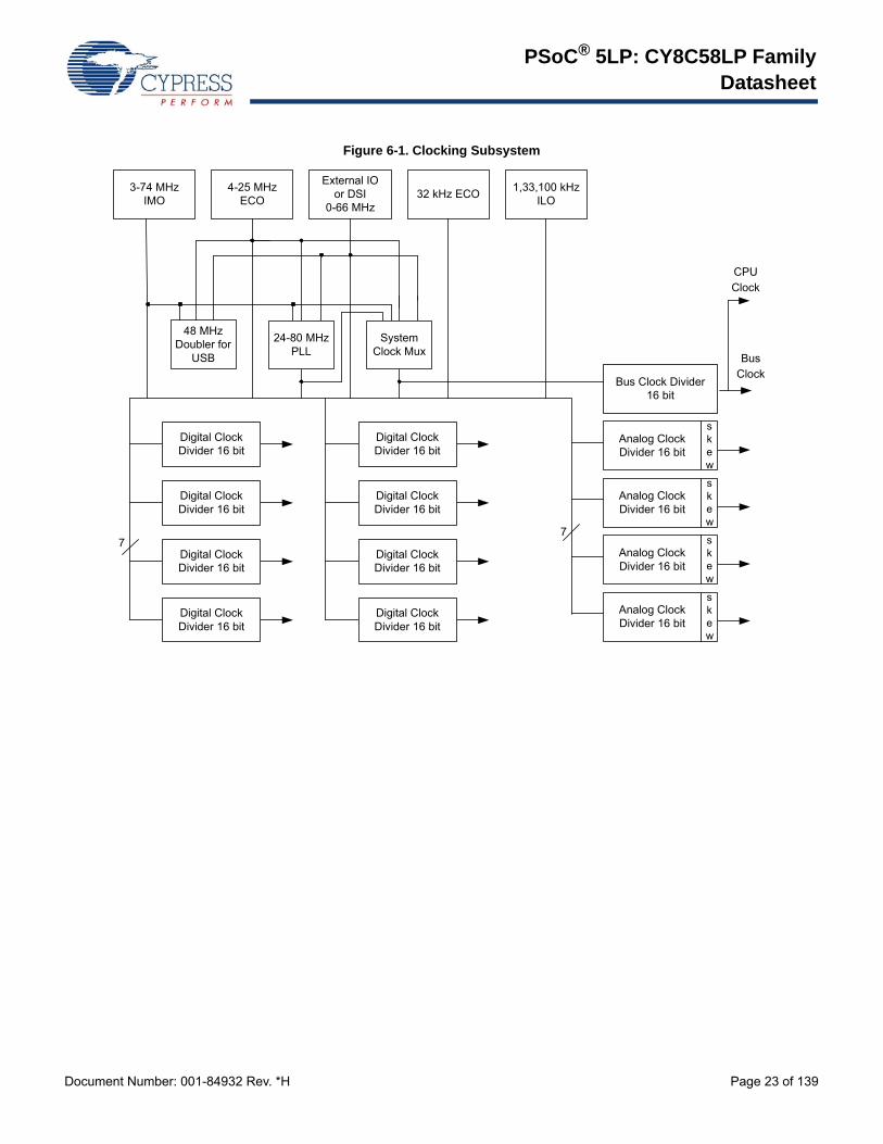
6. System Integration
6.1 Clocking System
The clocking system generates, divides, and distributes clocksthroughout the PSoC system. For the majority of systems, noexternal crystal is required. The IMO and PLL together cangenerate up to a 80 MHz clock, accurate to ±1% over voltage andtemperature. Additional internal and external clock sources alloweach design to optimize accuracy, power, and cost. All of thesystem clock sources can be used to generate other clockfrequencies in the 16-bit clock dividers and UDBs for anythingyou want, for example a UART baud rate generator.
Clock generation and distribution is automatically configuredthrough the PSoC Creator IDE graphical interface. This is basedon the complete system’s requirements. It greatly speeds thedesign process. PSoC Creator allows designers to build clockingsystems with minimal input. The designer can specify desiredclock frequencies and accuracies, and the software locates orbuilds a clock that meets the required specifications. This ispossible because of the programmability inherent in PSoC.
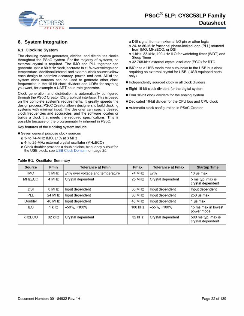
Key features of the clocking system include:
Seven general purpose clock sources 3- to 74-MHz IMO, ±1% at 3 MHz 4- to 25-MHz external crystal oscillator (MHzECO) Clock doubler provides a doubled clock frequency output for
the USB block, see USB Clock Domain on page 25.
DSI signal from an external I/O pin or other logic 24- to 80-MHz fractional phase-locked loop (PLL) sourced
from IMO, MHzECO, or DSI 1-kHz, 33-kHz, 100-kHz ILO for watchdog timer (WDT) and
Sleep Timer 32.768-kHz external crystal oscillator (ECO) for RTC
IMO has a USB mode that auto-locks to the USB bus clock requiring no external crystal for USB. (USB equipped parts only)
Independently sourced clock in all clock dividers
Eight 16-bit clock dividers for the digital system
Four 16-bit clock dividers for the analog system
Dedicated 16-bit divider for the CPU bus and CPU clock
Automatic clock configuration in PSoC Creator
Table 6-1. Oscillator Summary
Source Fmin Tolerance at Fmin Fmax Tolerance at Fmax Startup Time
IMO 3 MHz ±1% over voltage and temperature 74 MHz ±7% 13 µs max
MHzECO 4 MHz Crystal dependent 25 MHz Crystal dependent 5 ms typ, max is crystal dependent
ILO 1 kHz –50%, +100% 100 kHz –55%, +100% 15 ms max in lowest power mode
kHzECO 32 kHz Crystal dependent 32 kHz Crystal dependent 500 ms typ, max is crystal dependent
PSoC® 5LP: CY8C58LP FamilyDatasheet
Document Number: 001-84932 Rev. *H Page 23 of 139
Figure 6-1. Clocking Subsystem
4-25 MHz ECO
3-74 MHz IMO
32 kHz ECO1,33,100 kHz
ILO
skew
77
Digital Clock Divider 16 bit
Digital Clock Divider 16 bit
Digital Clock Divider 16 bit
Digital Clock Divider 16 bit
Digital Clock Divider 16 bit
Digital Clock Divider 16 bit
Digital Clock Divider 16 bit
Digital Clock Divider 16 bit
Analog Clock Divider 16 bit
Bus Clock Divider 16 bit
48 MHzDoubler for
USB
24-80 MHz PLL
System Clock Mux
External IOor DSI
0-66 MHz
skew
Analog Clock Divider 16 bit
skew
Analog Clock Divider 16 bit
skew
Analog Clock Divider 16 bit
Bus Clock
CPU Clock
PSoC® 5LP: CY8C58LP FamilyDatasheet
Document Number: 001-84932 Rev. *H Page 24 of 139
6.1.1 Internal Oscillators
Figure 6-1 shows that there are two internal oscillators. They canbe routed directly or divided. The direct routes may not have a50% duty cycle. Divided clocks have a 50% duty cycle.
6.1.1.1 Internal Main Oscillator
In most designs the IMO is the only clock source required, dueto its ±1% accuracy. The IMO operates with no externalcomponents and outputs a stable clock. A factory trim for eachfrequency range is stored in the device. With the factory trim,tolerance varies from ±1% at 3 MHz, up to ±7% at 74 MHz. TheIMO, in conjunction with the PLL, allows generation of CPU andsystem clocks up to the device's maximum frequency (see USBClock Domain on page 25). The IMO provides clock outputs at3, 6, 12, 24, 48, and 74 MHz.
6.1.1.2 Clock Doubler
The clock doubler outputs a clock at twice the frequency of theinput clock. The doubler works at input frequency of 24 MHz,providing 48 MHz for the USB. It can be configured to use a clockfrom the IMO, MHzECO, or the DSI (external pin).
6.1.1.3 Phase-Locked Loop
The PLL allows low frequency, high accuracy clocks to bemultiplied to higher frequencies. This is a tradeoff betweenhigher clock frequency and accuracy and, higher powerconsumption and increased startup time.
The PLL block provides a mechanism for generating clockfrequencies based upon a variety of input sources. The PLLoutputs clock frequencies in the range of 24 to 80 MHz. Its inputand feedback dividers supply 4032 discrete ratios to createalmost any desired system clock frequency. The accuracy of thePLL output depends on the accuracy of the PLL input source.The most common PLL use is to multiply the IMO clock at 3 MHz,where it is most accurate, to generate the CPU and systemclocks up to the device’s maximum frequency.
The PLL achieves phase lock within 250 µs (verified by bitsetting). It can be configured to use a clock from the IMO,MHzECO, or DSI (external pin). The PLL clock source can beused until lock is complete and signaled with a lock bit. The locksignal can be routed through the DSI to generate an interrupt.Disable the PLL before entering low power modes.
6.1.1.4 Internal Low-Speed Oscillator
The ILO provides clock frequencies for low power consumption,including the watchdog timer, and sleep timer. The ILOgenerates up to three different clocks: 1 kHz, 33 kHz, and100 kHz.
The 1-kHz clock (CLK1K) is typically used for a background‘heartbeat’ timer. This clock inherently lends itself to low powersupervisory operations such as the watchdog timer and longsleep intervals using the central timewheel (CTW).
The central timewheel is a 1 kHz, free running, 13-bit counterclocked by the ILO. The central timewheel is always enabledexcept in hibernate mode and when the CPU is stopped duringdebug on chip mode. It can be used to generate periodicinterrupts for timing purposes or to wake the system from a lowpower mode. Firmware can reset the central timewheel.
The central timewheel can be programmed to wake the systemperiodically and optionally issue an interrupt. This enablesflexible, periodic wakeups from low power modes or coarsetiming applications. Systems that require accurate timing shoulduse the RTC capability instead of the central timewheel.
The 100-kHz clock (CLK100K) can be used as a low powersystem clock to run the CPU. It can also generate time intervalsusing the fast timewheel.
The fast timewheel is a 5-bit counter, clocked by the 100-kHzclock. It features programmable settings and automaticallyresets when the terminal count is reached. An optional interruptcan be generated each time the terminal count is reached. Thisenables flexible, periodic interrupts of the CPU at a higher ratethan is allowed using the central timewheel.
The 33-kHz clock (CLK33K) comes from a divide-by-3 operationon CLK100K. This output can be used as a reduced accuracyversion of the 32.768-kHz ECO clock with no need for a crystal.
6.1.2 External Oscillators
Figure 6-1 shows that there are two external oscillators. Theycan be routed directly or divided. The direct routes may not havea 50% duty cycle. Divided clocks have a 50% duty cycle.
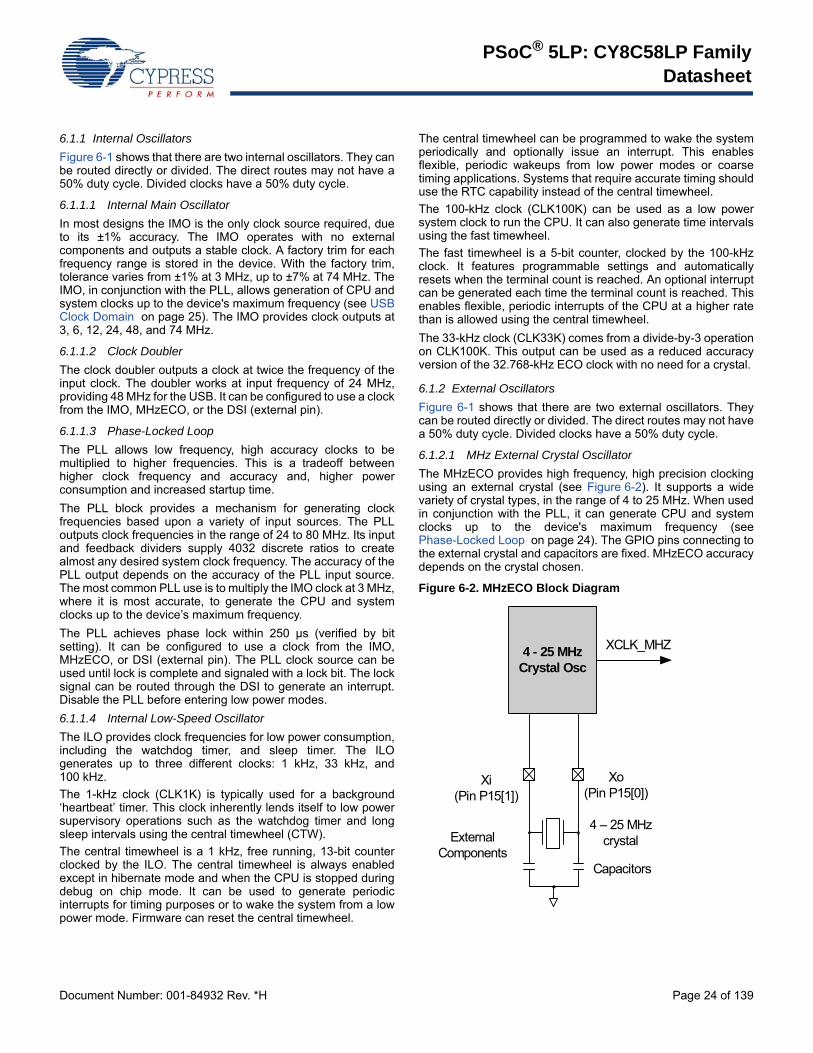
6.1.2.1 MHz External Crystal Oscillator
The MHzECO provides high frequency, high precision clockingusing an external crystal (see Figure 6-2). It supports a widevariety of crystal types, in the range of 4 to 25 MHz. When usedin conjunction with the PLL, it can generate CPU and systemclocks up to the device's maximum frequency (seePhase-Locked Loop on page 24). The GPIO pins connecting tothe external crystal and capacitors are fixed. MHzECO accuracydepends on the crystal chosen.
Figure 6-2. MHzECO Block Diagram
Xo(Pin P15[0])
4 - 25 MHz Crystal Osc
XCLK_MHZ
4 – 25 MHz crystal
Capacitors
External Components
Xi(Pin P15[1])
PSoC® 5LP: CY8C58LP FamilyDatasheet
Document Number: 001-84932 Rev. *H Page 25 of 139
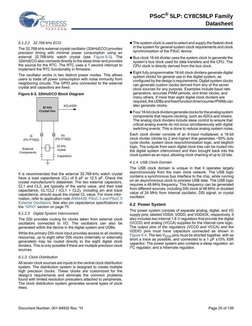
6.1.2.2 32.768 kHz ECO
The 32.768-kHz external crystal oscillator (32kHzECO) providesprecision timing with minimal power consumption using anexternal 32.768-kHz watch crystal (see Figure 6-3). The32kHzECO also connects directly to the sleep timer and providesthe source for the RTC. The RTC uses a 1 second interrupt toimplement the RTC functionality in firmware.
The oscillator works in two distinct power modes. This allowsusers to trade off power consumption with noise immunity fromneighboring circuits. The GPIO pins connected to the externalcrystal and capacitors are fixed.
Figure 6-3. 32kHzECO Block Diagram
It is recommended that the external 32.768-kHz watch crystalhave a load capacitance (CL) of 6 pF or 12.5 pF. Check thecrystal manufacturer's datasheet. The two external capacitors,CL1 and CL2, are typically of the same value, and their totalcapacitance, CL1CL2 / (CL1 + CL2), including pin and tracecapacitance, should equal the crystal CL value. For more infor-mation, refer to application note AN54439: PSoC 3 and PSoC 5External Oscillators. See also pin capacitance specifications inthe “GPIO” section on page 75.
6.1.2.3 Digital System Interconnect
The DSI provides routing for clocks taken from external clockoscillators connected to I/O. The oscillators can also begenerated within the device in the digital system and UDBs.
While the primary DSI clock input provides access to all clockingresources, up to eight other DSI clocks (internally or externallygenerated) may be routed directly to the eight digital clockdividers. This is only possible if there are multiple precision clocksources.
6.1.3 Clock Distribution
All seven clock sources are inputs to the central clock distributionsystem. The distribution system is designed to create multiplehigh precision clocks. These clocks are customized for thedesign’s requirements and eliminate the common problemsfound with limited resolution prescalers attached to peripherals.The clock distribution system generates several types of clocktrees.
The system clock is used to select and supply the fastest clock in the system for general system clock requirements and clock synchronization of the PSoC device.
Bus clock 16-bit divider uses the system clock to generate the system’s bus clock used for data transfers and the CPU. The CPU clock is directly derived from the bus clock.
Eight fully programmable 16-bit clock dividers generate digital system clocks for general use in the digital system, as configured by the design’s requirements. Digital system clocks can generate custom clocks derived from any of the seven clock sources for any purpose. Examples include baud rate generators, accurate PWM periods, and timer clocks, and many others. If more than eight digital clock dividers are required, the UDBs and fixed function timer/counter/PWMs can also generate clocks.
Four 16-bit clock dividers generate clocks for the analog system components that require clocking, such as ADCs and mixers. The analog clock dividers include skew control to ensure that critical analog events do not occur simultaneously with digital switching events. This is done to reduce analog system noise.
Each clock divider consists of an 8-input multiplexer, a 16-bitclock divider (divide by 2 and higher) that generates ~50% dutycycle clocks, system clock resynchronization logic, and deglitchlogic. The outputs from each digital clock tree can be routed intothe digital system interconnect and then brought back into theclock system as an input, allowing clock chaining of up to 32 bits.
6.1.4 USB Clock Domain
The USB clock domain is unique in that it operates largelyasynchronously from the main clock network. The USB logiccontains a synchronous bus interface to the chip, while runningon an asynchronous clock to process USB data. The USB logicrequires a 48-MHz frequency. This frequency can be generatedfrom different sources, including DSI clock at 48 MHz or doubledvalue of 24 MHz from internal oscillator, DSI signal, or crystaloscillator.
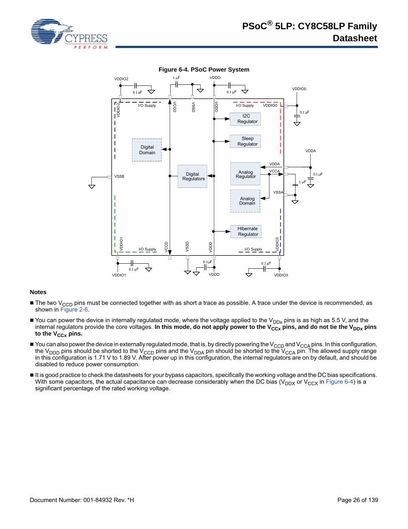
6.2 Power System
The power system consists of separate analog, digital, and I/Osupply pins, labeled VDDA, VDDD, and VDDIOX, respectively. Italso includes two internal 1.8 V regulators that provide the digital(VCCD) and analog (VCCA) supplies for the internal core logic.The output pins of the regulators (VCCD and VCCA) and theVDDIO pins must have capacitors connected as shown inFigure 6-4. The two VCCD pins must be shorted together, with asshort a trace as possible, and connected to a 1 µF ±10% X5Rcapacitor. The power system also contains a sleep regulator, anI2C regulator, and a hibernate regulator.
The two VCCD pins must be connected together with as short a trace as possible. A trace under the device is recommended, as shown in Figure 2-6.
You can power the device in internally regulated mode, where the voltage applied to the VDDx pins is as high as 5.5 V, and the internal regulators provide the core voltages. In this mode, do not apply power to the VCCx pins, and do not tie the VDDx pins to the VCCx pins.
You can also power the device in externally regulated mode, that is, by directly powering the VCCD and VCCA pins. In this configuration, the VDDD pins should be shorted to the VCCD pins and the VDDA pin should be shorted to the VCCA pin. The allowed supply range in this configuration is 1.71 V to 1.89 V. After power up in this configuration, the internal regulators are on by default, and should be disabled to reduce power consumption.
It is good practice to check the datasheets for your bypass capacitors, specifically the working voltage and the DC bias specifications. With some capacitors, the actual capacitance can decrease considerably when the DC bias (VDDX or VCCX in Figure 6-4) is a significant percentage of the rated working voltage.
VSSB
VS
SD
VD
DIO
1V
DD
IO2 VDDIO0
VD
DIO
3
VC
CD
VD
DD
VS
SD
VC
CD
VD
DD
VSSA
VCCA
VDDA
Digital Regulators
Analog Regulator
Analog Domain
Digital Domain
I2C Regulator
Sleep Regulator
Hibernate Regulator
I/O Supply I/O Supply
I/O SupplyI/O Supply
.
VDDIO2
VDDIO0
VDDIO3VDDIO1
0.1 µF
0.1 µF
0.1 µF
0.1 µF
VDDD
VDDD
1 µF
1 µF
VDDA
0.1 µF
0.1 µF
0.1µF
PSoC® 5LP: CY8C58LP FamilyDatasheet
Document Number: 001-84932 Rev. *H Page 27 of 139
6.2.1 Power Modes
PSoC 5LP devices have four different power modes, as shownin Table 6-2 and Table 6-3. The power modes allow a design toeasily provide required functionality and processing power whilesimultaneously minimizing power consumption and maximizingbattery life in low power and portable devices.
PSoC 5LP power modes, in order of decreasing powerconsumption are:
Active
Alternate active
Sleep
Hibernate
Active is the main processing mode. Its functionality isconfigurable. Each power controllable subsystem is enabled ordisabled by using separate power configuration templateregisters. In alternate active mode, fewer subsystems areenabled, reducing power. In sleep mode most resources aredisabled regardless of the template settings. Sleep mode isoptimized to provide timed sleep intervals and RTC functionality.The lowest power mode is hibernate, which retains register andSRAM state, but no clocks, and allows wakeup only from I/Opins. Figure 6-5 illustrates the allowable transitions betweenpower modes. Sleep and hibernate modes should not be entereduntil all VDDIO supplies are at valid voltage levels.
Table 6-2. Power Modes
Power Modes Description Entry Condition Wakeup Source Active Clocks Regulator
Active Primary mode of operation, all peripherals available (program-mable)
Wakeup, reset, manual register entry
Any interrupt Any (program-mable)
All regulators available. Digital and analog regulators can be disabled if external regulation used.
Alternate Active
Similar to Active mode, and is typically configured to have fewer peripherals active to reduce power. One possible configuration is to use the UDBs for processing, with the CPU turned off
Manual register entry
Any interrupt Any (program-mable)
All regulators available. Digital and analog regulators can be disabled if external regulation used.
Sleep All subsystems automatically disabled
Manual register entry
Comparator, PICU, I2C, RTC, CTW, LVD
ILO/kHzECO Both digital and analog regulators buzzed. Digital and analog regulators can be disabled if external regulation used.
Hibernate All subsystems automatically disabled Lowest power consuming mode with all peripherals and internal regulators disabled, except hibernate regulator is enabledConfiguration and memory contents retained
Manual register entry
PICU Only hibernate regulator active.
Table 6-3. Power Modes Wakeup Time and Power Consumption
Sleep Modes
Wakeup Time
Current (Typ)
Code Execution
Digital Resources
Analog Resources
Clock Sources Available Wakeup Sources Reset
Sources
Active – 3.1 mA[7] Yes All All All – All
Alternate Active
– – User defined
All All All – All
Sleep<25 µs 2 µA No I2C Comparator ILO/kHzECO Comparator, PICU,
I2C, RTC, CTW, LVD
XRES, LVD, WDR
Hibernate <200 µs 300 nA No None None None PICU XRES
Note7. Bus clock off. Execute from CPU instruction buffer at 6 MHz. See Table 11-2 on page 66.
PSoC® 5LP: CY8C58LP FamilyDatasheet
Document Number: 001-84932 Rev. *H Page 28 of 139
Figure 6-5. Power Mode Transitions
6.2.1.1 Active Mode
Active mode is the primary operating mode of the device. Whenin active mode, the active configuration template bits controlwhich available resources are enabled or disabled. When aresource is disabled, the digital clocks are gated, analog biascurrents are disabled, and leakage currents are reduced asappropriate. User firmware can dynamically control subsystempower by setting and clearing bits in the active configurationtemplate. The CPU can disable itself, in which case the CPU isautomatically reenabled at the next wakeup event.
When a wakeup event occurs, the global mode is alwaysreturned to active, and the CPU is automatically enabled,regardless of its template settings. Active mode is the defaultglobal power mode upon boot.
6.2.1.2 Alternate Active Mode
Alternate Active mode is very similar to Active mode. In alternateactive mode, fewer subsystems are enabled, to reduce powerconsumption. One possible configuration is to turn off the CPUand flash, and run peripherals at full speed.
6.2.1.3 Sleep Mode
Sleep mode reduces power consumption when a resume time of15 µs is acceptable. The wake time is used to ensure that theregulator outputs are stable enough to directly enter activemode.
6.2.1.4 Hibernate Mode
In hibernate mode nearly all of the internal functions aredisabled. Internal voltages are reduced to the minimal level tokeep vital systems alive. Configuration state is preserved inhibernate mode and SRAM memory is retained. GPIOsconfigured as digital outputs maintain their previous values andexternal GPIO pin interrupt settings are preserved. The devicecan only return from hibernate mode in response to an externalI/O interrupt. The resume time from hibernate mode is less than100 µs.
To achieve an extremely low current, the hibernate regulator haslimited capacity. This limits the frequency of any signal presenton the input pins; no GPIO should toggle at a rate greater than10 kHz while in hibernate mode. If pins must be toggled at a highrate while in a low power mode, use sleep mode instead.
6.2.1.5 Wakeup Events
Wakeup events are configurable and can come from an interruptor device reset. A wakeup event restores the system to activemode. Firmware enabled interrupt sources include internallygenerated interrupts, power supervisor, central timewheel, andI/O interrupts. Internal interrupt sources can come from a varietyof peripherals, such as analog comparators and UDBs. Thecentral timewheel provides periodic interrupts to allow thesystem to wake up, poll peripherals, or perform real-timefunctions. Reset event sources include the external reset I/O pin(XRES), WDT, and Precision Reset (PRES).
6.2.2 Boost Converter
Applications that use a supply voltage of less than 1.71 V, suchas solar panels or single cell battery supplies, may use theon-chip boost converter to generate a minimum of 1.8 V supplyvoltage. The boost converter may also be used in any systemthat requires a higher operating voltage than the supply providessuch as driving 5.0 V LCD glass in a 3.3 V system. With theaddition of an inductor, Schottky diode, and capacitors, itproduces a selectable output voltage sourcing enough current tooperate the PSoC and other on-board components.
The boost converter accepts an input voltage VBAT from 0.5 V to3.6 V, and can start up with VBAT as low as 0.5 V. The converterprovides a user configurable output voltage of 1.8 to 5.0 V (VOUT)in 100 mV increments. VBAT is typically less than VOUT; if VBAT isgreater than or equal to VOUT, then VOUT will be slightly less thanVBAT due to resistive losses in the boost converter. The block candeliver up to 50 mA (IBOOST) depending on configuration to boththe PSoC device and external components. The sum of allcurrent sinks in the design including the PSoC device, PSoC I/Opin loads, and external component loads must be less than theIBOOST specified maximum current.
Four pins are associated with the boost converter: VBAT, VSSB,VBOOST, and IND. The boosted output voltage is sensed at theVBOOST pin and must be connected directly to the chip’s supplyinputs; VDDA, VDDD, and VDDIO if used to power the PSoCdevice.
The boost converter requires four components in addition tothose required in a non-boost design, as shown in Figure 6-6 onpage 29. A 22 µF capacitor (CBAT) is required close to the VBATpin to provide local bulk storage of the battery voltage andprovide regulator stability. A diode between the battery and VBATpin should not be used for reverse polarity protection becausethe diodes forward voltage drop reduces the VBAT voltage.Between the VBAT and IND pins, an inductor of 4.7 µH, 10 µH,or 22 µH is required. The inductor value can be optimized toincrease the boost converter efficiency based on input voltage,output voltage, temperature, and current. Inductor size isdetermined by following the design guidance in this chapter andelectrical specifications. The Inductor must be placed within 1 cmof the VBAT and IND pins and have a minimum saturationcurrent of 750 mA. Between the IND and VBOOST pins aSchottky diode must be placed within 1 cm of the pins. TheSchottky diode shall have a forward current rating of at least 1.0A and a reverse voltage of at least 20 V. A 22 µF bulk capacitor(CBOOST) must be connected close to VBOOST to provideregulator output stability. It is important to sum the totalcapacitance connected to the VBOOST pin and ensure themaximum CBOOST specification is not exceeded. All capacitors
Active
Manual
Hibernate
Alternate Active
Sleep
PSoC® 5LP: CY8C58LP FamilyDatasheet
Document Number: 001-84932 Rev. *H Page 29 of 139
must be rated for a minimum of 10 V to minimize capacitivelosses due to voltage de-rating.
Figure 6-6. Application of Boost Converter powering PSoC device
The boost converter may also generate a supply that is not useddirectly by the PSoC device. An example of this use case isboosting a 1.8 V supply to 4.0 V to drive a white LED. If the boostconverter is not supplying the PSoC devices VDDA, VDDD, andVDDIO it must comply with the same design rules as supplying
the PSoC device, but with a change to the bulk capacitorrequirements. A parallel arrangement 22 µF, 1.0 µF, and 0.1 µFcapacitors are all required on the Vout supply and must beplaced within 1 cm of the VBOOST pin to ensure regulatorstability.
Figure 6-7. Application of Boost Converter not powering PSoC device
VBOOST
VBAT
VSSB
IND
VDDD
VDDA
VDDIO0
VSSA
VSSD
Boost Logic
VDDIO1
VDDIO2
VDDIO3
0.1 µF
0.1 µF
0.1 µF
0.1 µF
22 µF
0.1 µF
0.1 µF
1.0 µF
1.0 µF
22 µF
4.7 µH10 µH22 µH
Schottky, 1A
VDDD 0.1 µF 1.0 µF
All components and values are required
0.5–3.6 V
PSoC
External Load
VBOOST
VBAT
VSSB
IND
VDDD
VDDA
VDDIO0
VSSA
VSSD
Boost Logic
VDDIO1
VDDIO2
VDDIO322 µF
4.7 µH10 µH22 µH
Schottky, 1A
VDDD
All components and values are required
0.5–3.6 V
22 µF 0.1 µF1.0 µF
VDDA, VDDD, and VDDIO connections per section 6.2 Power System.
VOUT
PSoCExternal Load
PSoC® 5LP: CY8C58LP FamilyDatasheet
Document Number: 001-84932 Rev. *H Page 30 of 139
The switching frequency is set to 400 kHz using an oscillatorintegrated into the boost converter. The boost converter can beoperated in two different modes: active and standby. Activemode is the normal mode of operation where the boost regulatoractively generates a regulated output voltage. In standby mode,most boost functions are disabled, thus reducing powerconsumption of the boost circuit. Only minimal power is provided,typically < 5 µA to power the PSoC device in Sleep mode. Theboost typically draws 250 µA in active mode and 25 µA instandby mode. The boost operating modes must be used inconjunction with chip power modes to minimize total powerconsumption. Table 6-4 lists the boost power modes available indifferent chip power modes.
6.2.2.1 Boost Firmware Requirements
To ensure boost inrush current is within specification at startup,the Enable Fast IMO During Startup value must be uncheckedin the PSoC Creator IDE. The Enable Fast IMO During Startupoption is found in PSoC Creator in the design wide resources(cydwr) file System tab. Un-checking this option configures thedevice to run at 12 MHz vs 48 MHz during startup whileconfiguring the device. The slower clock speed results inreduced current draw through the boost circuit.
6.2.2.2 Boost Design Process
Correct operation of the boost converter requires specificcomponent values determined for each designs uniqueoperating conditions. The CBAT capacitor, Inductor, Schottkydiode, and CBOOST capacitor components are required with thevalues specified in the electrical specifications, Table 11-7 onpage 73. The only variable component value is the inductorLBOOST which is primarily sized for correct operation of the boostacross operating conditions and secondarily for efficiency.Additional operating region constraints exist for VOUT, VBAT, IOUT,and TA.
The following steps must be followed to determine boostconverter operating parameters and LBOOST value.
1. Choose desired VBAT, VOUT, TA, and IOUT operating condition ranges for the application.
2. Determine if VBAT and VOUT ranges fit the boost operating range based on the TA range over VBAT and VOUT chart, Figure 11-8 on page 73. If the operating ranges are not met, modify the operating conditions or use an external boost regulator.
3. Determine if the desired ambient temperature (TA) range fits the ambient temperature operating range based on the TA range over VBAT and VOUT chart, Figure 11-8 on page 73. If the temperature range is not met, modify the operating condi-tions and return to step 2, or use an external boost regulator.
4. Determine if the desired output current (IOUT) range fits the output current operating range based on the IOUT range over VBAT and VOUT chart, Figure 11-9 on page 73. If the output current range is not met, modify the operating conditions and return to step 2, or use an external boost regulator.
5. Find the allowed inductor values based on the LBOOST values over VBAT and VOUT chart, Figure 11-10 on page 73.
6. Based on the allowed inductor values, inductor dimensions, inductor cost, boost efficiency, and VRIPPLE choose the optimum inductor value for the system. Boost efficiency and VRIPPLE typical values are provided in the Efficiency vs VBAT and VRIPPLE vs VBAT charts, Figure 11-11 on page 74 through Figure 11-14 on page 74. In general, if high efficiency and low VRIPPLE are most important, then the highest allowed inductor value should be used. If low inductor cost or small inductor size are most important, then one of the smaller allowed inductor values should be used. If the allowed inductor(s) efficiency, VRIPPLE, cost or dimensions are not acceptable for the application than an external boost regulator should be used.
6.3 Reset
CY8C58LP has multiple internal and external reset sourcesavailable. The reset sources are: Power source monitoring - The analog and digital power
voltages, VDDA, VDDD, VCCA, and VCCD are monitored in several different modes during power up, active mode, and sleep mode (buzzing). If any of the voltages goes outside predetermined ranges then a reset is generated. The monitors are programmable to generate an interrupt to the processor under certain conditions before reaching the reset thresholds.
External - The device can be reset from an external source by pulling the reset pin (XRES) low. The XRES pin includes an internal pull-up to VDDIO1. VDDD, VDDA, and VDDIO1 must all have voltage applied before the part comes out of reset.
Watchdog timer - A watchdog timer monitors the execution of instructions by the processor. If the watchdog timer is not reset by firmware within a certain period of time, the watchdog timer generates a reset.
Software - The device can be reset under program control.
Table 6-4. Chip and Boost Power Modes Compatibility
Chip Power Modes Boost Power Modes
Chip-active or alternate active mode
Boost must be operated in its active mode.
Chip-sleep mode Boost can be operated in either active or standby mode. In boost standby mode, the chip must wake up periodi-cally for boost active-mode refresh.
Chip-hibernate mode Boost can be operated in its active mode. However, it is recommended not to use the boost in chip hibernate mode due to the higher current consumption in boost active mode.
PSoC® 5LP: CY8C58LP FamilyDatasheet
Document Number: 001-84932 Rev. *H Page 31 of 139
Figure 6-7. Resets
The term system reset indicates that the processor as well asanalog and digital peripherals and registers are reset.
A reset status register shows some of the resets or power voltagemonitoring interrupts. The program may examine this register todetect and report certain exception conditions. This register iscleared after a power-on reset. For details see the TechnicalReference Manual.
6.3.1 Reset Sources
6.3.1.1 Power Voltage Level Monitors IPOR - Initial Power-on-Reset
At initial power on, IPOR monitors the power voltages VDDD, VDDA, VCCD and VCCA. The trip level is not precise. It is set to approximately 1 volt, which is below the lowest specified operating voltage but high enough for the internal circuits to be reset and to hold their reset state. The monitor generates a reset pulse that is at least 150 ns wide. It may be much wider if one or more of the voltages ramps up slowly.If after the IPOR triggers either VDDX drops back below the trigger point, in a non-monotonic fashion, it must remain below that point for at least 10 µs. The hysteresis of the IPOR trigger point is typically 100 mV.
After boot, the IPOR circuit is disabled and voltage supervision is handed off to the precise low-voltage reset (PRES) circuit. PRES - Precise Low-Voltage Reset
This circuit monitors the outputs of the analog and digitalinternal regulators after power up. The regulator outputs arecompared to a precise reference voltage. The response to aPRES trip is identical to an IPOR reset.In normal operating mode, the program cannot disable thedigital PRES circuit. The analog regulator can be disabled,which also disables the analog portion of the PRES. The PREScircuit is disabled automatically during sleep and hibernatemodes, with one exception: During sleep mode the regulatorsare periodically activated (buzzed) to provide supervisoryservices and to reduce wakeup time. At these times the PREScircuit is also buzzed to allow periodic voltage monitoring.After PRES has been deasserted, at least 10 µs must elapsebefore it can be reasserted.
ALVI, DLVI, AHVI - Analog/Digital Low Voltage Interrupt, Analog High Voltage Interrupt Interrupt circuits are available to detect when VDDA andVDDD go outside a voltage range. For AHVI, VDDA iscompared to a fixed trip level. For ALVI and DLVI, VDDA andVDDD are compared to trip levels that are programmable, aslisted in Table 6-5. ALVI and DLVI can also be configured togenerate a device reset instead of an interrupt.
The monitors are disabled until after IPOR. During sleep modethese circuits are periodically activated (buzzed). If an interruptoccurs during buzzing then the system first enters its wakeupsequence. The interrupt is then recognized and may beserviced.
The buzz frequency is adjustable, and should be set to be lessthan the minimum time that any voltage is expected to be outof range. For details on how to adjust the buzz frequency, seethe TRM.
Reset Controller
Watchdog Timer
External Reset
Power Voltage Level
Monitors
Software Reset
Register
VDDD VDDA
Reset Pin
SystemReset
ProcessorInterrupt
Table 6-5. Analog/Digital Low Voltage Interrupt, Analog High Voltage Interrupt
Interrupt Supply Normal Voltage Range
Available TripSettings
DLVI VDDD 1.71 V-5.5 V 1.70 V-5.45 V in 250 mV increments
ALVI VDDA 1.71 V-5.5 V 1.70 V-5.45 V in 250 mV increments
AHVI VDDA 1.71 V-5.5 V 5.75 V
PSoC® 5LP: CY8C58LP FamilyDatasheet
Document Number: 001-84932 Rev. *H Page 32 of 139
6.3.1.2 Other Reset Sources
XRES - External Reset
PSoC 5LP has either a single GPIO pin that is configured asan external reset or a dedicated XRES pin. Either thededicated XRES pin or the GPIO pin, if configured, holds thepart in reset while held active (low). The response to an XRESis the same as to an IPOR reset. The external reset is activelow. It includes an internal pull-up resistor. XRES is activeduring sleep and hibernate modes.
After XRES has been deasserted, at least 10 µs must elapsebefore it can be reasserted.
SRES - Software Reset
A reset can be commanded under program control by settinga bit in the software reset register. This is done either directlyby the program or indirectly by DMA access. The response toa SRES is the same as after an IPOR reset.
Another register bit exists to disable this function.
WRES - Watchdog Timer Reset
The watchdog reset detects when the software program is nolonger being executed correctly. To indicate to the watchdogtimer that it is running correctly, the program must periodicallyreset the timer. If the timer is not reset before a user-specifiedamount of time, then a reset is generated.
Note IPOR disables the watchdog function. The program mustenable the watchdog function at an appropriate point in thecode by setting a register bit. When this bit is set, it cannot becleared again except by an IPOR power on reset event.
6.4 I/O System and Routing
PSoC I/Os are extremely flexible. Every GPIO has analog anddigital I/O capability. All I/Os have a large number of drive modes,which are set at POR. PSoC also provides up to four individualI/O voltage domains through the VDDIO pins.
There are two types of I/O pins on every device; those with USBprovide a third type. Both general purpose I/O (GPIO) andspecial I/O (SIO) provide similar digital functionality. The primarydifferences are their analog capability and drive strength.Devices that include USB also provide two USBIO pins thatsupport specific USB functionality as well as limited GPIOcapability.
All I/O pins are available for use as digital inputs and outputs forboth the CPU and digital peripherals. In addition, all I/O pins cangenerate an interrupt. The flexible and advanced capabilities ofthe PSoC I/O, combined with any signal to any pin routability,
greatly simplify circuit design and board layout. All GPIO pins canbe used for analog input, CapSense[8], and LCD segment drive,while SIO pins are used for voltages in excess of VDDA and forprogrammable output voltages.
Features supported by both GPIO and SIO: User programmable port reset state Separate I/O supplies and voltages for up to four groups of I/O Digital peripherals use DSI to connect the pins Input or output or both for CPU and DMA Eight drive modes Every pin can be an interrupt source configured as rising
edge, falling edge or both edges. If required, level sensitive interrupts are supported through the DSI
Dedicated port interrupt vector for each port Slew rate controlled digital output drive mode Access port control and configuration registers on either port
basis or pin basis Separate port read (PS) and write (DR) data registers to avoid
read modify write errors Special functionality on a pin by pin basis
Additional features only provided on the GPIO pins: LCD segment drive on LCD equipped devices CapSense[8]
Analog input and output capability Continuous 100 µA clamp current capability Standard drive strength down to 1.71 V
Additional features only provided on SIO pins: Higher drive strength than GPIO Hot swap capability (5 V tolerance at any operating VDD) Programmable and regulated high input and output drive
levels down to 1.2 V No analog input, CapSense, or LCD capability Over voltage tolerance up to 5.5 V SIO can act as a general purpose analog comparator
USBIO features: Full speed USB 2.0 compliant I/O Highest drive strength for general purpose use Input, output, or both for CPU and DMA Input, output, or both for digital peripherals Digital output (CMOS) drive mode Each pin can be an interrupt source configured as rising
edge, falling edge, or both edges
Note8. GPIOs with opamp outputs are not recommended for use with CapSense.
PSoC® 5LP: CY8C58LP FamilyDatasheet
Document Number: 001-84932 Rev. *H Page 33 of 139
Figure 6-8. GPIO Block Diagram
DriveLogic
PRT[x]DM0
PRT[x]DR
PIN
Digital Output Path
Digital Input Path
PRT[x]SLW
LCD
Logic & MUX
PRT[x]DM1PRT[x]DM2
PRT[x]LCD_EN
PRT[x]LCD_COM_SEG
Analog
Analog Mux
Analog Global
Digital System Output0
1
PRT[x]BYP
PRT[x]BIEBidirectional Control
Capsense Global Control
Switches
Pin Interrupt Signal
Digital System Input
PRT[x]PS
PRT[x]CTL
Input Buffer Disable
Display Data
Interrupt Logic
PICU[x]INTTYPE[y]
PICU[x]INTSTAT
Vddio
Vddio Vddio
Slew Cntl
LCD Bias Bus 5
PRT[x]AMUX
PRT[x]AG
1
CAPS[x]CFG1
OE
In
PRT[x]SYNC_OUT
PRT[x]DBL_SYNC_IN
PICU[x]INTSTAT
Naming Convention ‘x’ = Port Number ‘y’ = Pin Number
0
1 0
1
PSoC® 5LP: CY8C58LP FamilyDatasheet
Document Number: 001-84932 Rev. *H Page 34 of 139
Figure 6-9. SIO Input/Output Block Diagram
Figure 6-10. USBIO Block Diagram
DriveLogic
PRT[x]DM0
PRT[x]DR
PIN
Digital Output Path
Digital Input Path
PRT[x]SLW
PRT[x]DM1PRT[x]DM2
Digital System Output0
1
PRT[x]BYP
PRT[x]BIEBidirectional Control
Pin Interrupt Signal
Digital System Input
PRT[x]PS
Input Buffer DisableInterrupt
Logic
PICU[x]INTTYPE[y]
PICU[x]INTSTAT
Slew Cntl
OE
In
PRT[x]SYNC_OUT
PRT[x]DBL_SYNC_IN
PICU[x]INTSTAT
PRT[x]SIO_DIFF Buffer Thresholds
DriverVhigh
PRT[x]SIO_CFG
PRT[x]SIO_HYST_EN
Naming Convention ‘x’ = Port Number ‘y’ = Pin Number
Reference Level
Reference Level
DriveLogic
PRT[15]DR1[7,6]
PIN
Digital Output Path
Digital Input Path
Digital System Output0
1
PRT[15]BYP
Pin Interrupt Signal
Digital System Input
USBIO_CR1[0,1]
Interrupt Logic
PICU[15]INTTYPE[y]
PICU[15]INTSTAT
In
PRT[15]DBL_SYNC_IN
PICU[15]INTSTAT
Naming Convention ‘y’ = Pin Number
VdddVdddVddd
5 k 1.5 k
D+ pin only
PRT[15]DM1[6]
USBIO_CR1[5] USB or I/O
D+ 1.5 k
D+ 5 k
D+ Open Drain
PRT[15]SYNC_OUT
USB SIE Control for USB Mode
USB Receiver Circuitry
Vddd
PRT[15]PS[6,7]
USBIO_CR1[2]
D- 5 kPRT[15]DM1[7]
D- Open Drain
PRT[15]DM0[6]
PRT[15]DM0[7]
PSoC® 5LP: CY8C58LP FamilyDatasheet
Document Number: 001-84932 Rev. *H Page 35 of 139
6.4.1 Drive Modes
Each GPIO and SIO pin is individually configurable into one ofthe eight drive modes listed in Table 6-6. Three configuration bitsare used for each pin (DM[2:0]) and set in the PRTxDM[2:0]registers. Figure 6-11 depicts a simplified pin view based oneach of the eight drive modes. Table 6-6 shows the I/O pin’s drivestate based on the port data register value or digital array signal
if bypass mode is selected. Note that the actual I/O pin voltageis determined by a combination of the selected drive mode andthe load at the pin. For example, if a GPIO pin is configured forresistive pull-up mode and driven high while the pin is floating,the voltage measured at the pin is a high logic state. If the sameGPIO pin is externally tied to ground then the voltageunmeasured at the pin is a low logic state.
2 Resistive pull-up[9] 0 1 0 Res High (5K) Strong Low
3 Resistive pull-down[9] 0 1 1 Strong High Res Low (5K)
4 Open drain, drives low 1 0 0 High-Z Strong Low
5 Open drain, drive high 1 0 1 Strong High High-Z
6 Strong drive 1 1 0 Strong High Strong Low
7 Resistive pull-up and pull-down[9] 1 1 1 Res High (5K) Res Low (5K)
OutIn
PinOutIn
PinOutIn
Pin OutIn
Pin
OutIn
PinOutIn
PinOutIn
Pin OutIn
Pin
0. High Impedance Analog
1. High Impedance Digital
2. Resistive Pull-Up 3. Resistive Pull-Down
4. Open Drain, Drives Low
5. Open Drain, Drives High
6. Strong Drive 7. Resistive Pull-Up and Pull-Down
VDD VDD
VDD VDD VDD
An An An An
AnAnAnAn
The ‘Out’ connection is driven from either the Digital System (when the Digital Output terminal is connected) or the Data Register (when HW connection is disabled). The ‘In’ connection drives the Pin State register, and the Digital System if the Digital Input terminal is enabled and connected. The ‘An’ connection connects to the Analog System.
Note9. Resistive pull-up and pull-down are not available with SIO in regulated output mode.
PSoC® 5LP: CY8C58LP FamilyDatasheet
Document Number: 001-84932 Rev. *H Page 36 of 139
The USBIO pins (P15[7] and P15[6]), when enabled for I/O mode, have limited drive mode control. The drive mode is set using thePRT15.DM0[7, 6] register. A resistive pull option is also available at the USBIO pins, which can be enabled using the PRT15.DM1[7,6] register. When enabled for USB mode, the drive mode control has no impact on the configuration of the USB pins. Unlike the GPIOand SIO configurations, the port wide configuration registers do not configure the USB drive mode bits. Table 6-7 shows the drivemode configuration for the USBIO pins.
High impedance analog
The default reset state with both the output driver and digitalinput buffer turned off. This prevents any current from flowingin the I/O’s digital input buffer due to a floating voltage. Thisstate is recommended for pins that are floating or that supportan analog voltage. High impedance analog pins do not providedigital input functionality.
To achieve the lowest chip current in sleep modes, all I/Osmust either be configured to the high impedance analog mode,or have their pins driven to a power supply rail by the PSoCdevice or by external circuitry.
High impedance digital
The input buffer is enabled for digital signal input. This is thestandard high impedance (HiZ) state recommended for digitalinputs.
Resistive pull-up or resistive pull-downResistive pull-up or pull-down, respectively, provides a seriesresistance in one of the data states and strong drive in theother. Pins can be used for digital input and output in thesemodes. Interfacing to mechanical switches is a commonapplication for these modes. Resistive pull-up and pull-downare not available with SIO in regulated output mode.
Open drain, drives high and open drain, drives low Open drain modes provide high impedance in one of the datastates and strong drive in the other. Pins can be used for digitalinput and output in these modes. A common application forthese modes is driving the I2C bus signal lines.
Strong driveProvides a strong CMOS output drive in either high or lowstate. This is the standard output mode for pins. Strong Drivemode pins must not be used as inputs under normalcircumstances. This mode is often used to drive digital outputsignals or external FETs.
Resistive pull-up and pull-downSimilar to the resistive pull-up and resistive pull-down modesexcept the pin is always in series with a resistor. The high data
state is pull-up while the low data state is pull-down. This modeis most often used when other signals that may cause shortscan drive the bus. Resistive pull-up and pull-down are notavailable with SIO in regulated output mode.
6.4.2 Pin RegistersRegisters to configure and interact with pins come in two formsthat may be used interchangeably. All I/O registers are available in the standard port form, whereeach bit of the register corresponds to one of the port pins. Thisregister form is efficient for quickly reconfiguring multiple portpins at the same time.
I/O registers are also available in pin form, which combines theeight most commonly used port register bits into a single registerfor each pin. This enables very fast configuration changes toindividual pins with a single register write.
6.4.3 Bidirectional Mode
High speed bidirectional capability allows pins to provide boththe high impedance digital drive mode for input signals and asecond user selected drive mode such as strong drive (set usingPRTxDM[2:0] registers) for output signals on the same pin,based on the state of an auxiliary control bus signal. Thebidirectional capability is useful for processor busses andcommunications interfaces such as the SPI Slave MISO pin thatrequires dynamic hardware control of the output buffer.
The auxiliary control bus routes up to 16 UDB or digital peripheralgenerated output enable signals to one or more pins.
6.4.4 Slew Rate Limited Mode
GPIO and SIO pins have fast and slow output slew rate optionsfor strong and open drain drive modes, not resistive drive modes.Because it results in reduced EMI, the slow edge rate option isrecommended for signals that are not speed critical, generallyless than 1 MHz. The fast slew rate is for signals between 1 MHzand 33 MHz. The slew rate is individually configurable for eachpin, and is set by the PRTxSLW registers.
1 0 Res High (5k) Strong Low Resistive Pull Up, Strong Low
1 1 Strong High Strong Low Strong Outputs
PSoC® 5LP: CY8C58LP FamilyDatasheet
Document Number: 001-84932 Rev. *H Page 37 of 139
6.4.5 Pin InterruptsAll GPIO and SIO pins are able to generate interrupts to thesystem. All eight pins in each port interface to their own PortInterrupt Control Unit (PICU) and associated interrupt vector.Each pin of the port is independently configurable to detect risingedge, falling edge, both edge interrupts, or to not generate aninterrupt.
Depending on the configured mode for each pin, each time aninterrupt event occurs on a pin, its corresponding status bit of theinterrupt status register is set to “1” and an interrupt request issent to the interrupt controller. Each PICU has its own interruptvector in the interrupt controller and the pin status registerproviding easy determination of the interrupt source down to thepin level.
Port pin interrupts remain active in all sleep modes allowing thePSoC device to wake from an externally generated interrupt.While level sensitive interrupts are not directly supported;Universal Digital Blocks (UDB) provide this functionality to thesystem when needed.
6.4.6 Input Buffer ModeGPIO and SIO input buffers can be configured at the port levelfor the default CMOS input thresholds or the optional LVTTLinput thresholds. All input buffers incorporate Schmitt triggers forinput hysteresis. Additionally, individual pin input buffers can bedisabled in any drive mode.
6.4.7 I/O Power SuppliesUp to four I/O pin power supplies are provided depending on thedevice and package. Each I/O supply must be less than or equalto the voltage on the chip’s analog (VDDA) pin. This featureallows users to provide different I/O voltage levels for differentpins on the device. Refer to the specific device package pinoutto determine VDDIO capability for a given port and pin. The SIOport pins support an additional regulated high output capability,as described in Adjustable Output Level.
6.4.8 Analog ConnectionsThese connections apply only to GPIO pins. All GPIO pins maybe used as analog inputs or outputs. The analog voltage presenton the pin must not exceed the VDDIO supply voltage to whichthe GPIO belongs. Each GPIO may connect to one of the analogglobal busses or to one of the analog mux buses to connect anypin to any internal analog resource such as ADC or comparators.In addition, select pins provide direct connections to specificanalog features such as the high current DACs or uncommittedopamps.
6.4.9 CapSenseThis section applies only to GPIO pins. All GPIO pins may beused to create CapSense buttons and sliders[10]. See the“CapSense” section on page 58 for more information.
6.4.10 LCD Segment DriveThis section applies only to GPIO pins. All GPIO pins may beused to generate Segment and Common drive signals for directglass drive of LCD glass. See the “LCD Direct Drive” section onpage 57 for details.
6.4.11 Adjustable Output Level
This section applies only to SIO pins. SIO port pins support theability to provide a regulated high output level for interface toexternal signals that are lower in voltage than the SIO’srespective VDDIO. SIO pins are individually configurable tooutput either the standard VDDIO level or the regulated output,which is based on an internally generated reference. Typically avoltage DAC (VDAC) is used to generate the reference (seeFigure 6-12). The “DAC” section on page 58 has more details onVDAC use and reference routing to the SIO pins. Resistivepull-up and pull-down drive modes are not available with SIO inregulated output mode.
6.4.12 Adjustable Input Level
This section applies only to SIO pins. SIO pins by default supportthe standard CMOS and LVTTL input levels but also support adifferential mode with programmable levels. SIO pins aregrouped into pairs. Each pair shares a reference generator blockwhich, is used to set the digital input buffer reference level forinterface to external signals that differ in voltage from VDDIO.The reference sets the pins voltage threshold for a high logiclevel (see Figure 6-12). Available input thresholds are: 0.5 VDDIO 0.4 VDDIO 0.5 VREF VREF
Typically a voltage DAC (VDAC) generates the VREF reference.DAC on page 58 has more details on VDAC use and referencerouting to the SIO pins.
Figure 6-12. SIO Reference for Input and Output
PIN
DriveLogic
DriverVhigh
Reference Generator
SIO_Ref
Digital Input
Digital Output
Input Path
Output Path
Vinref
Voutref
Note10. GPIOs with opamp outputs are not recommended for use with CapSense.
PSoC® 5LP: CY8C58LP FamilyDatasheet
Document Number: 001-84932 Rev. *H Page 38 of 139
6.4.13 SIO as Comparator
This section applies only to SIO pins. The adjustable input levelfeature of the SIOs as explained in the Adjustable Input Level onpage 37 can be used to construct a comparator. The thresholdfor the comparator is provided by the SIO's reference generator.The reference generator has the option to set the analog signalrouted through the analog global line as threshold for thecomparator. Note that a pair of SIO pins share the samethreshold.
The digital input path in Figure 6-9 on page 34 illustrates thisfunctionality. In the figure, ‘Reference level’ is the analog signalrouted through the analog global. The hysteresis feature canalso be enabled for the input buffer of the SIO, which increasesnoise immunity for the comparator.
6.4.14 Hot Swap
This section applies only to SIO pins. SIO pins support ‘hot swap’capability to plug into an application without loading the signalsthat are connected to the SIO pins even when no power isapplied to the PSoC device. This allows the unpowered PSoC tomaintain a high impedance load to the external device while alsopreventing the PSoC from being powered through a SIO pin’sprotection diode.
Powering the device up or down while connected to anoperational I2C bus may cause transient states on the SIO pins.The overall I2C bus design should take this into account.
6.4.15 Overvoltage Tolerance
All I/O pins provide an overvoltage tolerance feature at anyoperating VDD.
There are no current limitations for the SIO pins as they present a high impedance load to the external circuit.
The GPIO pins must be limited to 100 µA using a current limiting resistor. GPIO pins clamp the pin voltage to approximately one diode above the VDDIO supply.
In case of a GPIO pin configured for analog input/output, the analog voltage on the pin must not exceed the VDDIO supply voltage to which the GPIO belongs.
A common application for this feature is connection to a bus suchas I2C where different devices are running from different supplyvoltages. In the I2C case, the PSoC chip is configured into theOpen Drain, Drives Low mode for the SIO pin. This allows anexternal pull-up to pull the I2C bus voltage above the PSoC pinsupply. For example, the PSoC chip could operate at 1.8 V, andan external device could run from 5 V. Note that the SIO pin’sVIH and VIL levels are determined by the associated VDDIOsupply pin.
The SIO pin must be in one of the following modes: 0 (highimpedance analog), 1 (high impedance digital), or 4 (open draindrives low). See Figure 6-11 for details. Absolute maximumratings for the device must be observed for all I/O pins.
6.4.16 Reset Configuration
While reset is active all I/Os are reset to and held in the HighImpedance Analog state. After reset is released, the state can bereprogrammed on a port-by-port basis to pull-down or pull-up. Toensure correct reset operation, the port reset configuration datais stored in special nonvolatile registers. The stored reset data isautomatically transferred to the port reset configuration registersat reset release.
6.4.17 Low Power Functionality
In all low power modes the I/O pins retain their state until the partis awakened and changed or reset. To awaken the part, use apin interrupt, because the port interrupt logic continues tofunction in all low power modes.
6.4.18 Special Pin Functionality
Some pins on the device include additional special functionalityin addition to their GPIO or SIO functionality. The specific specialfunction pins are listed in “Pinouts” on page 6. The specialfeatures are:
Digital 4- to 25-MHz crystal oscillator 32.768-kHz crystal oscillator Wake from sleep on I2C address match. Any pin can be used
for I2C if wake from sleep is not required. JTAG interface pins SWD interface pins SWV interface pins TRACEPORT interface pins External reset
Analog Opamp inputs and outputs High current IDAC outputs External reference inputs
6.4.19 JTAG Boundary Scan
The device supports standard JTAG boundary scan chains on allpins for board level test.
PSoC® 5LP: CY8C58LP FamilyDatasheet
Document Number: 001-84932 Rev. *H Page 39 of 139
7. Digital Subsystem
The digital programmable system creates application specificcombinations of both standard and advanced digital peripheralsand custom logic functions. These peripherals and logic are theninterconnected to each other and to any pin on the device,providing a high level of design flexibility and IP security.
The features of the digital programmable system are outlinedhere to provide an overview of capabilities and architecture. Youdo not need to interact directly with the programmable digitalsystem at the hardware and register level. PSoC Creatorprovides a high level schematic capture graphical interface toautomatically place and route resources similar to PLDs.
The main components of the digital programmable system are:
Universal Digital Blocks (UDB) - These form the core functionality of the digital programmable system. UDBs are a collection of uncommitted logic (PLD) and structural logic (Datapath) optimized to create all common embedded peripherals and customized functionality that are application or design specific.
Universal Digital Block array - UDB blocks are arrayed within a matrix of programmable interconnect. The UDB array structure is homogeneous and allows for flexible mapping of digital functions onto the array. The array supports extensive and flexible routing interconnects between UDBs and the Digital System Interconnect.
Digital System Interconnect (DSI) - Digital signals from Universal Digital Blocks (UDBs), fixed function peripherals, I/O pins, interrupts, DMA, and other system core signals are attached to the Digital System Interconnect to implement full featured device connectivity. The DSI allows any digital function to any pin or other feature routability when used with the Universal Digital Block array.
Figure 7-1. CY8C58LP Digital Programmable Architecture
7.1 Example Peripherals
The flexibility of the CY8C58LP family’s UDBs and analog blocksallow the user to create a wide range of components(peripherals). The most common peripherals were built andcharacterized by Cypress and are shown in the PSoC Creatorcomponent catalog, however, users may also create their owncustom components using PSoC Creator. Using PSoC Creator,users may also create their own components for reuse withintheir organization, for example sensor interfaces, proprietaryalgorithms, and display interfaces.
The number of components available through PSoC Creator istoo numerous to list in the datasheet, and the list is alwaysgrowing. An example of a component available for use inCY8C58LP family, but, not explicitly called out in this datasheetis the UART component.
7.1.1 Example Digital Components
The following is a sample of the digital components available inPSoC Creator for the CY8C58LP family. The exact amount ofhardware resources (UDBs, routing, RAM, flash) used by acomponent varies with the features selected in PSoC Creator forthe component.
Communications I2C UART SPI
Functions EMIF PWMs Timers Counters
Logic NOT OR XOR AND
7.1.2 Example Analog Components
The following is a sample of the analog components available inPSoC Creator for the CY8C58LP family. The exact amount ofhardware resources (SC/CT blocks, routing, RAM, flash) usedby a component varies with the features selected in PSoCCreator for the component.
Amplifiers TIA PGA opamp
ADCs Delta-Sigma Successive Approximation (SAR)
DACs Current Voltage PWM
Comparators
Mixers
IO P
ort
Digital Core System and Fixed Function Peripherals
UD
B A
rray
UD
B A
rray
IO P
ort
IO P
ort
IO P
ort DSI Routing Interface
DSI Routing Interface
Digital Core System and Fixed Function Peripherals
UDB UDB UDB UDB
UDB UDB UDB UDB
UDB UDB UDB UDB
UDB UDB UDB UDB
UDB UDB UDB UDB
UDB UDB UDB UDB
PSoC® 5LP: CY8C58LP FamilyDatasheet
Document Number: 001-84932 Rev. *H Page 40 of 139
7.1.3 Example System Function Components
The following is a sample of the system function componentsavailable in PSoC Creator for the CY8C58LP family. The exactamount of hardware resources (UDBs, DFB taps, SC/CT blocks,routing, RAM, flash) used by a component varies with thefeatures selected in PSoC Creator for the component.
CapSense
LCD Drive
LCD Control
Filters
7.1.4 Designing with PSoC Creator
7.1.4.1 More Than a Typical IDE
A successful design tool allows for the rapid development anddeployment of both simple and complex designs. It reduces oreliminates any learning curve. It makes the integration of a newdesign into the production stream straightforward.
PSoC Creator is that design tool.
PSoC Creator is a full featured Integrated DevelopmentEnvironment (IDE) for hardware and software design. It isoptimized specifically for PSoC devices and combines a modern,powerful software development platform with a sophisticatedgraphical design tool. This unique combination of tools makesPSoC Creator the most flexible embedded design platformavailable.
Graphical design entry simplifies the task of configuring aparticular part. You can select the required functionality from anextensive catalog of components and place it in your design. Allcomponents are parameterized and have an editor dialog thatallows you to tailor functionality to your needs.
PSoC Creator automatically configures clocks and routes the I/Oto the selected pins and then generates APIs to give theapplication complete control over the hardware. Changing thePSoC device configuration is as simple as adding a newcomponent, setting its parameters, and rebuilding the project.
At any stage of development you are free to change thehardware configuration and even the target processor. Toretarget your application (hardware and software) to newdevices, even from 8- to 32-bit families, just select the newdevice and rebuild.
You also have the ability to change the C compiler and evaluatean alternative. Components are designed for portability and arevalidated against all devices, from all families, and against allsupported tool chains. Switching compilers is as easy as editingthe from the project options and rebuilding the application withno errors from the generated APIs or boot code.
7.1.4.2 Component Catalog
The component catalog is a repository of reusable designelements that select device functionality and customize yourPSoC device. It is populated with an impressive selection ofcontent; from simple primitives such as logic gates and deviceregisters, through the digital timers, counters and PWMs, plusanalog components such as ADCs, DACs, and filters, andcommunication protocols, such as I2C, USB, and CAN. SeeExample Peripherals on page 39 for more details aboutavailable peripherals. All content is fully characterized andcarefully documented in datasheets with code examples, AC/DCspecifications, and user code ready APIs.
7.1.4.3 Design Reuse
The symbol editor gives you the ability to develop reusablecomponents that can significantly reduce future design time. Justdraw a symbol and associate that symbol with your provendesign. PSoC Creator allows for the placement of the newsymbol anywhere in the component catalog along with thecontent provided by Cypress. You can then reuse your contentas many times as you want, and in any number of projects,without ever having to revisit the details of the implementation.
7.1.4.4 Software Development
Anchoring the tool is a modern, highly customizable userinterface. It includes project management and integrated editorsfor C and assembler source code, as well the design entry tools.Project build control leverages compiler technology from topcommercial vendors such as ARM® Limited, Keil™, andCodeSourcery (GNU). Free versions of Keil C51 and GNU CCompiler (GCC) for ARM, with no restrictions on code size or endproduct distribution, are included with the tool distribution.Upgrading to more optimizing compilers is a snap with supportfor the professional Keil C51 product and ARM RealView™compiler.
7.1.4.5 Nonintrusive Debugging
With JTAG (4-wire) and SWD (2-wire) debug connectivityavailable on all devices, the PSoC Creator debugger offers fullcontrol over the target device with minimum intrusion.Breakpoints and code execution commands are all readilyavailable from toolbar buttons and an impressive lineup ofwindows—register, locals, watch, call stack, memory andperipherals—make for an unparalleled level of visibility into thesystem. PSoC Creator contains all the tools necessary tocomplete a design, and then to maintain and extend that designfor years to come. All steps of the design flow are carefullyintegrated and optimized for ease-of-use and to maximizeproductivity.
PSoC® 5LP: CY8C58LP FamilyDatasheet
Document Number: 001-84932 Rev. *H Page 41 of 139
7.2 Universal Digital Block
The Universal Digital Block (UDB) represents an evolutionarystep to the next generation of PSoC embedded digital peripheralfunctionality. The architecture in first generation PSoC digitalblocks provides coarse programmability in which a few fixedfunctions with a small number of options are available. The newUDB architecture is the optimal balance between configurationgranularity and efficient implementation. A cornerstone of thisapproach is to provide the ability to customize the devices digitaloperation to match application requirements.
To achieve this, UDBs consist of a combination of uncommittedlogic (PLD), structured logic (Datapath), and a flexible routingscheme to provide interconnect between these elements, I/Oconnections, and other peripherals. UDB functionality rangesfrom simple self contained functions that are implemented in oneUDB, or even a portion of a UDB (unused resources areavailable for other functions), to more complex functions thatrequire multiple UDBs. Examples of basic functions are timers,counters, CRC generators, PWMs, dead band generators, andcommunications functions, such as UARTs, SPI, and I2C. Also,the PLD blocks and connectivity provide full featured generalpurpose programmable logic within the limits of the availableresources.
Figure 7-2. UDB Block Diagram
The main component blocks of the UDB are: PLD blocks - There are two small PLDs per UDB. These blocks
take inputs from the routing array and form registered or combinational sum-of-products logic. PLDs are used to implement state machines, state bits, and combinational logic equations. PLD configuration is automatically generated from graphical primitives.
Datapath Module - This 8-bit wide datapath contains structured logic to implement a dynamically configurable ALU, a variety of compare configurations and condition generation. This block also contains input/output FIFOs, which are the primary parallel data interface between the CPU/DMA system and the UDB.
Status and Control Module - The primary role of this block is to provide a way for CPU firmware to interact and synchronize with UDB operation.
Clock and Reset Module - This block provides the UDB clocks and reset selection and control.
7.2.1 PLD Module
The primary purpose of the PLD blocks is to implement logicexpressions, state machines, sequencers, look up tables, anddecoders. In the simplest use model, consider the PLD blocks asa standalone resource onto which general purpose RTL issynthesized and mapped. The more common and efficient usemodel is to create digital functions from a combination of PLDand datapath blocks, where the PLD implements only therandom logic and state portion of the function while the datapath(ALU) implements the more structured elements.
Figure 7-3. PLD 12C4 Structure
One 12C4 PLD block is shown in Figure 7-3. This PLD has 12inputs, which feed across eight product terms. Each product term(AND function) can be from 1 to 12 inputs wide, and in a givenproduct term, the true (T) or complement (C) of each input canbe selected. The product terms are summed (OR function) tocreate the PLD outputs. A sum can be from 1 to 8 product termswide. The 'C' in 12C4 indicates that the width of the OR gate (inthis case 8) is constant across all outputs (rather than variableas in a 22V10 device). This PLA like structure gives maximumflexibility and insures that all inputs and outputs are permutablefor ease of allocation by the software tools. There are two 12C4PLDs in each UDB.
7.2.2 Datapath Module
The datapath contains an 8-bit single cycle ALU, with associatedcompare and condition generation logic. This datapath block isoptimized to implement embedded functions, such as timers,counters, integrators, PWMs, PRS, CRC, shifters and dead bandgenerators, and many others.
PLD 12C4
(8 PTs)
PLD 12C4
(8 PTs)
Datapath
Clock and Reset
Control
Routing Channel
Datapath Chaining
PLD Chaining
Status and Control
PT
0
IN0
IN1
IN2
IN3
IN4
IN5
IN6
IN7
IN8
IN9
IN10
IN11
T C T C T C T C T C T C T C T C
T C T C T C T C T C T C T C T C
T C T C T C T C T C T C T C T C
T C T C T C T C T C T C T C T C
T C T C T C T C T C T C T C T C
T C T C T C T C T C T C T C T C
T C T C T C T C T C T C T C T C
T C T C T C T C T C T C T C T C
T C T C T C T C T C T C T C T C
T C T C T C T C T C T C T C T C
T C T C T C T C T C T C T C T C
T C T C T C T C T C T C T C T C
PT
1
PT
2
PT
3
PT
4
PT
5
PT
6
PT
7
T T T T T T T T
T T T T T T T T
T T T T T T T T
T T T T T T T T
AND Array
OR Array
MC0
MC1
MC2
OUT0
OUT1
OUT2
OUT3MC3
Carry In
Carry Out
PSoC® 5LP: CY8C58LP FamilyDatasheet
Document Number: 001-84932 Rev. *H Page 42 of 139
Figure 7-4. Datapath Top Level
7.2.2.1 Working Registers
The datapath contains six primary working registers, which areaccessed by CPU firmware or DMA during normal operation.
7.2.2.2 Dynamic Configuration RAM
Dynamic configuration is the ability to change the datapathfunction and internal configuration on a cycle-by-cycle basis,under sequencer control. This is implemented using the 8-wordx 16-bit configuration RAM, which stores eight unique 16-bit wideconfigurations. The address input to this RAM controls the
sequence, and can be routed from any block connected to theUDB routing matrix, most typically PLD logic, I/O pins, or fromthe outputs of this or other datapath blocks.
ALU
The ALU performs eight general purpose functions. They are:
Increment
Decrement
Add
Subtract
Logical AND
Logical OR
Logical XOR
Pass, used to pass a value through the ALU to the shift register, mask, or another UDB register
Independent of the ALU operation, these functions are available:
A0 and A1 Accumulators These are sources and sinks for the ALU and also sources for the compares.
D0 and D1 Data Registers These are sources for the ALU and sources for the compares.
F0 and F1 FIFOs These are the primary interface to the system bus. They can be a data source for the data registers and accumulators or they can capture data from the accumu-lators or ALU. Each FIFO is four bytes deep.
PSoC® 5LP: CY8C58LP FamilyDatasheet
Document Number: 001-84932 Rev. *H Page 43 of 139
7.2.2.3 Conditionals
Each datapath has two compares, with bit masking options.Compare operands include the two accumulators and the twodata registers in a variety of configurations. Other conditionsinclude zero detect, all ones detect, and overflow. Theseconditions are the primary datapath outputs, a selection of whichcan be driven out to the UDB routing matrix. Conditionalcomputation can use the built in chaining to neighboring UDBsto operate on wider data widths without the need to use routingresources.
7.2.2.4 Variable MSB
The most significant bit of an arithmetic and shift function can beprogrammatically specified. This supports variable width CRCand PRS functions, and in conjunction with ALU output masking,can implement arbitrary width timers, counters and shift blocks.
7.2.2.5 Built-in CRC/PRS
The datapath has built in support for single cycle CyclicRedundancy Check (CRC) computation and Pseudo RandomSequence (PRS) generation of arbitrary width and arbitrarypolynomial. CRC/PRS functions longer than 8 bits may beimplemented in conjunction with PLD logic, or built in chainingmay be use to extend the function into neighboring UDBs.
7.2.2.6 Input/Output FIFOs
Each datapath contains two four-byte deep FIFOs, which can beindependently configured as an input buffer (system bus writesto the FIFO, datapath internal reads the FIFO), or an outputbuffer (datapath internal writes to the FIFO, the system bus readsfrom the FIFO). The FIFOs generate status that are selectableas datapath outputs and can therefore be driven to the routing,to interact with sequencers, interrupts, or DMA.
Figure 7-5. Example FIFO Configurations
7.2.2.7 Chaining
The datapath can be configured to chain conditions and signalssuch as carries and shift data with neighboring datapaths tocreate higher precision arithmetic, shift, CRC/PRS functions.
7.2.2.8 Time Multiplexing
In applications that are over sampled, or do not need high clockrates, the single ALU block in the datapath can be efficientlyshared with two sets of registers and condition generators. Carryand shift out data from the ALU are registered and can beselected as inputs in subsequent cycles. This provides supportfor 16-bit functions in one (8-bit) datapath.
7.2.2.9 Datapath I/O
There are six inputs and six outputs that connect the datapath tothe routing matrix. Inputs from the routing provide theconfiguration for the datapath operation to perform in each cycle,and the serial data inputs. Inputs can be routed from other UDBblocks, other device peripherals, device I/O pins, and so on. Theoutputs to the routing can be selected from the generatedconditions, and the serial data outputs. Outputs can be routed toother UDB blocks, device peripherals, interrupt and DMAcontroller, I/O pins, and so on.
7.2.3 Status and Control Module
The primary purpose of this circuitry is to coordinate CPUfirmware interaction with internal UDB operation.
Figure 7-6. Status and Control Registers
The bits of the control register, which may be written to by thesystem bus, are used to drive into the routing matrix, and thusprovide firmware with the opportunity to control the state of UDBprocessing. The status register is read-only and it allows internalUDB state to be read out onto the system bus directly frominternal routing. This allows firmware to monitor the state of UDBprocessing. Each bit of these registers has programmableconnections to the routing matrix and routing connections aremade depending on the requirements of the application.
7.2.3.1 Usage Examples
As an example of control input, a bit in the control register canbe allocated as a function enable bit. There are multiple ways toenable a function. In one method the control bit output would berouted to the clock control block in one or more UDBs and serveas a clock enable for the selected UDB blocks. A status exampleis a case where a PLD or datapath block generated a condition,such as a “compare true” condition that is captured and latchedby the status register and then read (and cleared) by CPUfirmware.
7.2.3.2 Clock Generation
Each subcomponent block of a UDB including the two PLDs, thedatapath, and Status and Control, has a clock selection andcontrol block. This promotes a fine granularity with respect toallocating clocking resources to UDB component blocks andallows unused UDB resources to be used by other functions formaximum system efficiency.
System Bus
F0
F1
System Bus
A0/A1/ALU
D0/D1
A0/A1/ALU
System Bus
F1
A0/A1/ALU
F0
D0
System Bus
F1
A0
D1
A1
F0
TX/RX Dual Capture Dual Buffer
Routing Channel
8-bit Status Register(Read Only)
8-bit Control Register(Write/Read)
System Bus
PSoC® 5LP: CY8C58LP FamilyDatasheet
Document Number: 001-84932 Rev. *H Page 44 of 139
7.3 UDB Array Description
Figure 7-7 shows an example of a 16 UDB array. In addition tothe array core, there are a DSI routing interfaces at the top andbottom of the array. Other interfaces that are not explicitly showninclude the system interfaces for bus and clock distribution. TheUDB array includes multiple horizontal and vertical routingchannels each comprised of 96 wires. The wire connections toUDBs, at horizontal/vertical intersection and at the DSI interfaceare highly permutable providing efficient automatic routing inPSoC Creator. Additionally the routing allows wire by wiresegmentation along the vertical and horizontal routing to furtherincrease routing flexibility and capability.
Figure 7-7. Digital System Interface Structure
7.3.1 UDB Array Programmable Resources
Figure 7-8 shows an example of how functions are mapped intoa bank of 16 UDBs. The primary programmable resources of theUDB are two PLDs, one datapath and one status/control register.These resources are allocated independently, because theyhave independently selectable clocks, and therefore unusedblocks are allocated to other unrelated functions.
An example of this is the 8-bit Timer in the upper left corner ofthe array. This function only requires one datapath in the UDB,and therefore the PLD resources may be allocated to anotherfunction. A function such as a Quadrature Decoder may requiremore PLD logic than one UDB can supply and in this case can
utilize the unused PLD blocks in the 8-bit Timer UDB.Programmable resources in the UDB array are generallyhomogeneous so functions can be mapped to arbitraryboundaries in the array.
Figure 7-8. Function Mapping Example in a Bank of UDBs
7.4 DSI Routing Interface Description
The DSI routing interface is a continuation of the horizontal andvertical routing channels at the top and bottom of the UDB arraycore. It provides general purpose programmable routingbetween device peripherals, including UDBs, I/Os, analogperipherals, interrupts, DMA and fixed function peripherals.
Figure 7-9 illustrates the concept of the digital systeminterconnect, which connects the UDB array routing matrix withother device peripherals. Any digital core or fixed functionperipheral that needs programmable routing is connected to thisinterface.
Signals in this category include:
Interrupt requests from all digital peripherals in the system.
DMA requests from all digital peripherals in the system.
Digital peripheral data signals that need flexible routing to I/Os.
Digital peripheral data signals that need connections to UDBs.
Connections to the interrupt and DMA controllers.
Connection to I/O pins.
Connection to analog system digital signals.
UDB
UDB
HVB
UDB
UDB
HVA
UDB
UDB
HVB
HVA
UDB
UDB
HVA
UDB
UDB
HVB
UDB
UDB
HVA
HVB
HVB
HVA
HVB
HVA
HVA
HVB
HVA
HVB
UDB
UDB
UDB
UDB
System Connections
System Connections
UDB
UDB
HVB
UDB
UDB
HVA
UDB
UDB
HVB
HVA
UDB
HVA
UDB
HVB
UDB
HVA
HVB
UDB
UDB
UDBUDBUDB UDB
UART
Logic
12-Bit PWM
I2C Slave8-Bit SPI
12-Bit SPI
Logic8-Bit Timer
16-Bit PYRS
UDB
8-Bit Timer
Quadrature Decoder 16-Bit PWM
Se
qu
ence
r
PSoC® 5LP: CY8C58LP FamilyDatasheet
Document Number: 001-84932 Rev. *H Page 45 of 139
Figure 7-9. Digital System Interconnect
Interrupt and DMA routing is very flexible in the CY8C58LPprogrammable architecture. In addition to the numerous fixedfunction peripherals that can generate interrupt requests, anydata signal in the UDB array routing can also be used to generatea request. A single peripheral may generate multipleindependent interrupt requests simplifying system and firmwaredesign. Figure 7-10 shows the structure of the IDMUX(Interrupt/DMA Multiplexer).
Figure 7-10. Interrupt and DMA Processing in the IDMUX
7.4.1 I/O Port Routing
There are a total of 20 DSI routes to a typical 8-bit I/O port, 16for data and four for drive strength control.
When an I/O pin is connected to the routing, there are twoprimary connections available, an input and an output. Inconjunction with drive strength control, this can implement abidirectional I/O pin. A data output signal has the option to be
single synchronized (pipelined) and a data input signal has theoption to be double synchronized. The synchronization clock isthe system clock (see Figure 6-1). Normally all inputs from pinsare synchronized as this is required if the CPU interacts with thesignal or any signal derived from it. Asynchronous inputs haverare uses. An example of this is a feed through of combinationalPLD logic from input pins to output pins.
Figure 7-11. I/O Pin Synchronization Routing
Figure 7-12. I/O Pin Output Connectivity
There are four more DSI connections to a given I/O port toimplement dynamic output enable control of pins. Thisconnectivity gives a range of options, from fully ganged 8-bitscontrolled by one signal, to up to four individually controlled pins.The output enable signal is useful for creating tri-statebidirectional pins and buses.
Figure 7-13. I/O Pin Output Enable Connectivity
UDB ARRAY
Digital System Routing I/F
Digital System Routing I/F
CANInterrupt
ControllerI2C
IO Port Pins
DMAController
IO Port Pins
Delta-Sigma ADC
ComparatorsDACSSC/CT Blocks
Global Clocks
EMIFGlobalClocks
TimerCounters
SAR ADC
DMA termout (IRQs)
DMA Controller
Interrupt Controller
Fixed Function IRQs
Edge Detect
Edge Detect
IRQs
UDB Array
Fixed Function DRQs
DRQs
Interrupt and DMA Processing in IDMUX
0
1
2
3
0
1
2
DO
DI
Port i
PIN 0DO
PIN1DO
PIN2DO
PIN3DO
PIN4DO
PIN5DO
PIN6DO
PIN7DO
8 IO Data Output Connections from the UDB Array Digital System Interface
Port i
PIN 0OE
PIN1OE
PIN2OE
PIN3OE
PIN4OE
PIN5OE
PIN6OE
PIN7OE
4 IO Control Signal Connections from UDB Array Digital System Interface
PSoC® 5LP: CY8C58LP FamilyDatasheet
Document Number: 001-84932 Rev. *H Page 46 of 139
7.5 CAN
The CAN peripheral is a fully functional Controller Area Network(CAN) supporting communication baud rates up to 1 Mbps. TheCAN controller implements the CAN2.0A and CAN2.0Bspecifications as defined in the Bosch specification andconforms to the ISO-11898-1 standard. The CAN protocol wasoriginally designed for automotive applications with a focus on ahigh level of fault detection. This ensures high communication
reliability at a low cost. Because of its success in automotiveapplications, CAN is used as a standard communication protocolfor motion oriented machine control networks (CANOpen) andfactory automation applications (DeviceNet). The CAN controllerfeatures allow the efficient implementation of higher levelprotocols without affecting the performance of themicrocontroller CPU. Full configuration support is provided inPSoC Creator.
Figure 7-14. CAN Bus System Implementation
7.5.1 CAN Features
CAN2.0A/B protocol implementation - ISO 11898 compliant Standard and extended frames with up to 8 bytes of data per
frame Message filter capabilities Remote Transmission Request (RTR) support Programmable bit rate up to 1 Mbps
Listen Only mode
SW readable error counter and indicator
Sleep mode: Wake the device from sleep with activity on the Rx pin
Supports two or three wire interface to external transceiver (Tx, Rx, and Enable). The three-wire interface is compatible with the Philips PHY; the PHY is not included on-chip. The three wires can be routed to any I/O
Enhanced interrupt controller CAN receive and transmit buffers status CAN controller error status including BusOff
Receive path 16 receive buffers each with its own message filter Enhanced hardware message filter implementation that
covers the ID, IDE and RTR DeviceNet addressing support Multiple receive buffers linkable to build a larger receive
message array Automatic transmission request (RTR) response handler Lost received message notification
CAN Controller configuration integrated into PSoC Creator:
CAN Configuration walkthrough with bit timing analyzer
Receive filter setup
CAN Node 1
PSoC
CAN Controller
CAN Transceiver
Tx RxEn
CAN Node 2 CAN Node n
CAN_H CAN_L CAN_H CAN_L CAN_H CAN_L
CAN Drivers
CAN Bus
PSoC® 5LP: CY8C58LP FamilyDatasheet
Document Number: 001-84932 Rev. *H Page 47 of 139
Figure 7-15. CAN Controller Block Diagram
7.6 USB
PSoC includes a dedicated Full-Speed (12 Mbps) USB 2.0transceiver supporting all four USB transfer types: control,interrupt, bulk, and isochronous. PSoC Creator provides fullconfiguration support. USB interfaces to hosts through twodedicated USBIO pins, which are detailed in the I/O System andRouting on page 32.
USB includes the following features:
Eight unidirectional data endpoints
One bidirectional control endpoint 0 (EP0)
Shared 512-byte buffer for the eight data endpoints
Dedicated 8-byte buffer for EP0
Three memory modes Manual Memory Management with No DMA Access Manual Memory Management with Manual DMA Access Automatic Memory Management with Automatic DMA
Access
Internal 3.3 V regulator for transceiver
Internal 48 MHz oscillator that auto locks to USB bus clock, requiring no external crystal for USB (USB equipped parts only)
Interrupts on bus and each endpoint event, with device wakeup
Error Status Error Active Error Passive Bus OffTx Error CounterRx Error Counter
ErrInterrupt Request
(if enabled)
WakeUp Request
Rx Buffer Status
RxMessage Available
Tx Buffer StatusTxReq
Pending
Rx
Tx
S I E (Serial Interface
Engine)
48 MHz IMO
Arbiter512 X 8 SRAM
USB I/O
D+
D–Interrupts
Sys
tem
Bus
External 22 Resistors
PSoC® 5LP: CY8C58LP FamilyDatasheet
Document Number: 001-84932 Rev. *H Page 48 of 139
7.7 Timers, Counters, and PWMs
The Timer/Counter/PWM peripheral is a 16-bit dedicatedperipheral providing three of the most common embeddedperipheral features. As almost all embedded systems use somecombination of timers, counters, and PWMs. Four of them havebeen included on this PSoC device family. Additional and moreadvanced functionality timers, counters, and PWMs can also beinstantiated in Universal Digital Blocks (UDBs) as required.PSoC Creator allows you to choose the timer, counter, and PWMfeatures that you need. The tool set utilizes the most optimalresources available.
The Timer/Counter/PWM peripheral can select from multipleclock sources, with input and output signals connected throughthe DSI routing. DSI routing allows input and output connectionsto any device pin and any internal digital signal accessiblethrough the DSI. Each of the four instances has a compareoutput, terminal count output (optional complementary compareoutput), and programmable interrupt request line. TheTimer/Counter/PWMs are configurable as free running, one shot,or Enable input controlled. The peripheral has timer reset andcapture inputs, and a kill input for control of the comparatoroutputs. The peripheral supports full 16-bit capture.
Timer/Counter/PWM features include:
16-bit timer/counter/PWM (down count only)
Selectable clock source
PWM comparator (configurable for LT, LTE, EQ, GTE, GT)
Period reload on start, reset, and terminal count
Interrupt on terminal count, compare true, or capture
Dynamic counter reads
Timer capture mode
Count while enable signal is asserted mode
Free run mode
One-shot mode (stop at end of period)
Complementary PWM outputs with deadband
PWM output kill
Figure 7-17. Timer/Counter/PWM
7.8 I2C
PSoC includes a single fixed-function I2C peripheral. AdditionalI2C interfaces can be instantiated using Universal Digital Blocks(UDBs) in PSoC Creator, as required.
The I2C peripheral provides a synchronous two-wire interfacedesigned to interface the PSoC device with a two-wire I2C serialcommunication bus. It is compatible[12] with I2C Standard-mode,Fast-mode, and Fast-mode Plus devices as defined in the NXPI2C-bus specification and user manual (UM10204). The I2C busI/O may be implemented with GPIO or SIO in open-drain modes.
To eliminate the need for excessive CPU intervention andoverhead, I2C specific support is provided for status detectionand generation of framing bits. I2C operates as a slave, a master,or multimaster (Slave and Master)[12]. In slave mode, the unitalways listens for a start condition to begin sending or receivingdata. Master mode supplies the ability to generate the Start andStop conditions and initiate transactions. Multimaster modeprovides clock synchronization and arbitration to allow multiplemasters on the same bus. If Master mode is enabled and Slavemode is not enabled, the block does not generate interrupts onexternally generated Start conditions. I2C interfaces through theDSI routing and allows direct connections to any GPIO or SIOpins.
I2C provides hardware address detect of a 7-bit address withoutCPU intervention. Additionally the device can wake from lowpower modes on a 7-bit hardware address match. If wakeupfunctionality is required, I2C pin connections are limited to one oftwo specific pairs of SIO pins. See descriptions of SCL and SDApins in Pin Descriptions on page 11.
I2C features include:
Slave and master, transmitter, and receiver operation
Byte processing for low CPU overhead
Interrupt or polling CPU interface
Support for bus speeds up to 1 Mbps
7 or 10-bit addressing (10-bit addressing requires firmware support)
SMBus operation (through firmware support - SMBus supported in hardware in UDBs)
7-bit hardware address compare
Wake from low power modes on address match
Glitch filtering (active and alternate-active modes only)
Data transfers follow the format shown in Figure 7-18. After theSTART condition (S), a slave address is sent. This address is 7bits long followed by an eighth bit which is a data direction bit(R/W) - a 'zero' indicates a transmission (WRITE), a 'one'indicates a request for data (READ). A data transfer is alwaysterminated by a STOP condition (P) generated by the master.
Timer / Counter / PWM 16-bit
ClockResetEnableCaptureKill
IRQ
Compare
TC / Compare!
Notes11. The I2C peripheral is non-compliant with the NXP I2C specification in the following areas: analog glitch filter, I/O VOL/IOL, I/O hysteresis. The I2C Block has a digital
glitch filter (not available in sleep mode). The Fast-mode minimum fall-time specification can be met by setting the I/Os to slow speed mode. See the I/O Electrical Specifications in Inputs and Outputs on page 75 for details.
12. Fixed-block I2C does not support undefined bus conditions, nor does it support Repeated Start in Slave mode. These conditions should be avoided, or the UDB-based I2C component should be used instead.
PSoC® 5LP: CY8C58LP FamilyDatasheet
Document Number: 001-84932 Rev. *H Page 49 of 139
Figure 7-18. I2C Complete Transfer Timing
7.8.1 External Electrical Connections
As Figure 7-19 shows, the I2C bus requires external pull-upresistors (RP). These resistors are primarily determined by thesupply voltage, bus speed, and bus capacitance. For detailedinformation on how to calculate the optimum pull-up resistorvalue for your design, we recommend using the UM10204I2C-bus specification and user manual Rev 6, or newer, availablefrom the NXP website at www.nxp.com.
Figure 7-19. Connection of Devices to the I2C Bus
For most designs, the default values in Table 7-2 will provideexcellent performance without any calculations. The defaultvalues were chosen to use standard resistor values between theminimum and maximum limits. The values in Table 7-2 work fordesigns with 1.8 V to 5.0V VDD, less than 200-pF bus capaci-tance (CB), up to 25 µA of total input leakage (IIL), up to 0.4 Voutput voltage level (VOL), and a max VIH of 0.7 * VDD. StandardMode and Fast Mode can use either GPIO or SIO PSoC pins.Fast Mode Plus requires use of SIO pins to meet the VOL specat 20 mA. Calculation of custom pull-up resistor values isrequired; if your design does not meet the default assumptions,you use series resistors (RS) to limit injected noise, or you needto maximize the resistor value for low power consumption.
Calculation of the ideal pull-up resistor value involves finding avalue between the limits set by three equations detailed in theNXP I2C specification. These equations are:
Equation 1:
Equation 2:
Equation 3:
Equation parameters:
VDD = Nominal supply voltage for I2C bus
VOL = Maximum output low voltage of bus devices.
IOL= Low-level output current from I2C specification
TR = Rise Time of bus from I2C specification
CB = Capacitance of each bus line including pins and PCB traces
VIH = Minimum high-level input voltage of all bus devices
VNH = Minimum high-level input noise margin from I2C specifi-cation
IIH = Total input leakage current of all devices on the bus
The supply voltage (VDD) limits the minimum pull-up resistorvalue due to bus devices maximum low output voltage (VOL)specifications. Lower pull-up resistance increases currentthough the pins and can, therefore, exceed the spec conditionsof VOH. Equation 1 is derived using Ohm's law to determine theminimum resistance that will still meet the VOL specification at3 mA for standard and fast modes, and 20 mA for fast mode plusat the given VDD.
Equation 2 determines the maximum pull-up resistance due tobus capacitance. Total bus capacitance is comprised of all pin,wire, and trace capacitance on the bus. The higher the buscapacitance, the lower the pull-up resistance required to meetthe specified bus speeds rise time due to RC delays. Choosinga pull-up resistance higher than allowed can result in failingtiming requirements resulting in communication errors. Mostdesigns with five or less I2C devices and up to 20 centimeters ofbus trace length have less than 100 pF of bus capacitance.
A secondary effect that limits the maximum pull-up resistor valueis total bus leakage calculated in Equation 3. The primary sourceof leakage is I/O pins connected to the bus. If leakage is too high,the pull-ups will have difficulty maintaining an acceptable VIHlevel causing communication errors. Most designs with five orless I2C devices on the bus have less than 10 µA of total leakagecurrent.
Some devices in the CY8C58LP family of devices have adedicated HW accelerator block used for digital filtering. TheDFB has a dedicated multiplier and accumulator that calculatesa 24-bit by 24-bit multiply accumulate in one system clock cycle.This enables the mapping of a direct form FIR filter thatapproaches a computation rate of one FIR tap for each clockcycle. The MCU can implement any of the functions performedby this block, but at a slower rate that consumes significant MCUbandwidth.
The PSoC Creator interface provides a wizard to implement FIRand IIR digital filters with coefficients for LPF, BPF, HPF, Notchand arbitrary shape filters. 64 pairs of data and coefficients arestored. This enables a 64 tap FIR filter or up to 4 16 tap filters ofeither FIR or IIR formulation.
Figure 7-20. DFB Application Diagram (pwr/gnd not shown)
The typical use model is for data to be supplied to the DFB overthe system bus from another on-chip system data source suchas an ADC. The data typically passes through main memory oris directly transferred from another chip resource through DMA.The DFB processes this data and passes the result to anotheron chip resource such as a DAC or main memory through DMAon the system bus.
Data movement in or out of the DFB is typically controlled by thesystem DMA controller but can be moved directly by the MCU.
8. Analog Subsystem
The analog programmable system creates application specificcombinations of both standard and advanced analog signalprocessing blocks. These blocks are then interconnected toeach other and also to any pin on the device, providing a highlevel of design flexibility and IP security. The features of theanalog subsystem are outlined here to provide an overview ofcapabilities and architecture.
Flexible, configurable analog routing architecture provided by analog globals, analog mux bus, and analog local buses
High resolution Delta-Sigma ADC
Two successive approximation (SAR) ADCs
Four 8-bit DACs that provide either voltage or current output
Four comparators with optional connection to configurable LUT outputs
Four configurable switched capacitor/continuos time (SC/CT) blocks for functions that include opamp, unity gain buffer, programmable gain amplifier, transimpedance amplifier, and mixer
Four opamps for internal use and connection to GPIO that can be used as high current output buffers
CapSense subsystem to enable capacitive touch sensing
Precision reference for generating an accurate analog voltage for internal analog blocks
Digital Filter Block
write_data
read_data
SystemBus
DMACTRL
DataSource (PHUB)
DataDest
(PHUB)
addrDigital
Routing
BUSCLK
DMA Request
PSoC® 5LP: CY8C58LP FamilyDatasheet
Document Number: 001-84932 Rev. *H Page 51 of 139
Figure 8-1. Analog Subsystem Block Diagram
The PSoC Creator software program provides a user friendlyinterface to configure the analog connections between the GPIOand various analog resources and also connections from oneanalog resource to another. PSoC Creator also providescomponent libraries that allow you to configure the variousanalog blocks to perform application specific functions (PGA,transimpedance amplifier, voltage DAC, current DAC, and soon). The tool also generates API interface libraries that allow youto write firmware that allows the communication between theanalog peripheral and CPU/Memory.
8.1 Analog Routing
The PSoC 5LP family of devices has a flexible analog routingarchitecture that provides the capability to connect GPIOs anddifferent analog blocks, and also route signals between differentanalog blocks. One of the strong points of this flexible routingarchitecture is that it allows dynamic routing of input and outputconnections to the different analog blocks.
For information on how to make pin selections for optimal analogrouting, refer to the application note, AN58304 - PSoC® 3 andPSoC® 5 - Pin Selection for Analog Designs.
8.1.1 Features
Flexible, configurable analog routing architecture
16 analog globals (AG) and two analog mux buses (AMUXBUS) to connect GPIOs and the analog blocks
Each GPIO is connected to one analog global and one analog mux bus
Eight analog local buses (abus) to route signals between the different analog blocks
Multiplexers and switches for input and output selection of the analog blocks
8.1.2 Functional Description
Analog globals (AGs) and analog mux buses (AMUXBUS)provide analog connectivity between GPIOs and the variousanalog blocks. There are 16 AGs in the PSoC 5LP family. Theanalog routing architecture is divided into four quadrants asshown in Figure 8-2. Each quadrant has four analog globals(AGL[0..3], AGL[4..7], AGR[0..3], AGR[4..7]). Each GPIO isconnected to the corresponding AG through an analog switch.The analog mux bus is a shared routing resource that connectsto every GPIO through an analog switch. There are twoAMUXBUS routes in PSoC 5LP, one in the left half (AMUXBUSL)and one in the right half (AMUXBUSR), as shown in Figure 8-2.
Analog local buses (abus) are routing resources located withinthe analog subsystem and are used to route signals betweendifferent analog blocks. There are eight abus routes in PSoC5LP, four in the left half (abusl [0:3]) and four in the right half(abusr [0:3]) as shown in Figure 8-2. Using the abus saves theanalog globals and analog mux buses from being used forinterconnecting the analog blocks.
Multiplexers and switches exist on the various buses to directsignals into and out of the analog blocks. A multiplexer can haveonly one connection on at a time, whereas a switch can havemultiple connections on simultaneously. In Figure 8-2,multiplexers are indicated by grayed ovals and switches areindicated by transparent ovals.
To preserve detail of this figure, this figure is best viewed with a PDF display program or printed on a 11” × 17” paper.
PSoC® 5LP: CY8C58LP FamilyDatasheet
Document Number: 001-84932 Rev. *H Page 53 of 139
8.2 Delta-sigma ADC
The CY8C58LP device contains one delta-sigma ADC. ThisADC offers differential input, high resolution and excellentlinearity, making it a good ADC choice for both audio signalprocessing and measurement applications. The converter'snominal operation is 16 bits at 48 ksps. The ADC can beconfigured to output 20-bit resolution at data rates of up to 187sps. At a fixed clock rate, resolution can be traded for faster datarates as shown in Table 8-1 and Figure 8-3.
Figure 8-3. Delta-sigma ADC Sample Rates, Range = ±1.024 V
8.2.1 Functional Description
The ADC connects and configures three basic components,input buffer, delta-sigma modulator, and decimator. The basicblock diagram is shown in Figure 8-4. The signal from the inputmuxes is delivered to the delta-sigma modulator either directly orthrough the input buffer. The delta-sigma modulator performs theactual analog to digital conversion. The modulator over-samplesthe input and generates a serial data stream output. This highspeed data stream is not useful for most applications withoutsome type of post processing, and so is passed to the decimatorthrough the Analog Interface block. The decimator converts thehigh speed serial data stream into parallel ADC results. Themodulator/decimator frequency response is [(sin x)/x]4.
Figure 8-4. Delta-sigma ADC Block Diagram
Resolution and sample rate are controlled by the Decimator.Data is pipelined in the decimator; the output is a function of thelast four samples. When the input multiplexer is switched, theoutput data is not valid until after the fourth sample after theswitch.
8.2.2 Operational Modes
The ADC can be configured by the user to operate in one of fourmodes: Single Sample, Multi Sample, Continuous, or MultiSample (Turbo). All four modes are started by either a write tothe start bit in a control register or an assertion of the Start ofConversion (SoC) signal. When the conversion is complete, astatus bit is set and the output signal End of Conversion (EoC)asserts high and remains high until the value is read by either theDMA controller or the CPU.
8.2.2.1 Single Sample
In Single Sample mode, the ADC performs one sampleconversion on a trigger. In this mode, the ADC stays in standbystate waiting for the SoC signal to be asserted. When SoC issignaled the ADC performs four successive conversions. Thefirst three conversions prime the decimator. The ADC result isvalid and available after the fourth conversion, at which time theEoC signal is generated. To detect the end of conversion, thesystem may poll a control register for status or configure theexternal EoC signal to generate an interrupt or invoke a DMArequest. When the transfer is done the ADC reenters the standbystate where it stays until another SoC event.
8.2.2.2 Continuous
Continuous sample mode is used to take multiple successivesamples of a single input signal. Multiplexing multiple inputsshould not be done with this mode. There is a latency of threeconversion times before the first conversion result is available.This is the time required to prime the decimator. After the firstresult, successive conversions are available at the selectedsample rate.
8.2.2.3 Multi Sample
Multi sample mode is similar to continuous mode except that theADC is reset between samples. This mode is useful when theinput is switched between multiple signals. The decimator isre-primed between each sample so that previous samples do notaffect the current conversion. Upon completion of a sample, thenext sample is automatically initiated. The results can betransferred using either firmware polling, interrupt, or DMA.
Table 8-1. Delta-sigma ADC Performance
Bits Maximum Sample Rate (sps) SINAD (dB)
20 187 –
16 48 k 84
12 192 k 66
8 384 k 43
1000
10000
100000
1000000
e R
ate,
sp
s
1
10
100
6 8 10 12 14 16 18 20 22
Sam
ple
Resolution, bits
Continuous Multi-Sample Multi-SampleTurbo
Delta Sigma
ModulatorDecimator 12 to 20 Bit
Result
EOC
SOC
PositiveInput Mux
NegativeInput Mux
(Analog Routing)InputBuffer
PSoC® 5LP: CY8C58LP FamilyDatasheet
Document Number: 001-84932 Rev. *H Page 54 of 139
8.2.2.4 Multi Sample (Turbo)
The multi sample (turbo) mode operates identical to theMulti-sample mode for resolutions of 8 to 16 bits. For resolutionsof 17 to 20 bits, the performance is about four times faster thanthe multi sample mode, because the ADC is only reset once atthe end of conversion.
More information on output formats is provided in the TechnicalReference Manual.
8.2.3 Start of Conversion Input
The SoC signal is used to start an ADC conversion. A digitalclock or UDB output can be used to drive this input. It can beused when the sampling period must be longer than the ADCconversion time or when the ADC must be synchronized to otherhardware. This signal is optional and does not need to beconnected if ADC is running in a continuous mode.
8.2.4 End of Conversion Output
The EoC signal goes high at the end of each ADC conversion.This signal may be used to trigger either an interrupt or DMArequest.
8.3 Successive Approximation ADC
The CY8C58LP family of devices has two SuccessiveApproximation (SAR) ADCs. These ADCs are 12-bit at up to 1Msps, with single-ended or differential inputs, making themuseful for a wide variety of sampling and control applications.
8.3.1 Functional Description
In a SAR ADC an analog input signal is sampled and comparedwith the output of a DAC. A binary search algorithm is applied tothe DAC and used to determine the output bits in successionfrom MSB to LSB. A block diagram of one SAR ADC is shown inFigure 8-5.
Figure 8-5. SAR ADC Block Diagram
The input is connected to the analog globals and muxes. Thefrequency of the clock is 18 times the sample rate; the clock rateranges from 1 to 18 MHz.
8.3.2 Conversion Signals
Writing a start bit or assertion of a start of frame (SOF) signal isused to start a conversion. SOF can be used in applicationswhere the sampling period is longer than the conversion time, orwhen the ADC needs to be synchronized to other hardware. Thissignal is optional and does not need to be connected if the SARADC is running in a continuous mode. A digital clock or UDBoutput can be used to drive this input. When the SAR is firstpowered up or awakened from any of the sleeping modes, thereis a power up wait time of 10 µs before it is ready to start the firstconversion.
When the conversion is complete, a status bit is set and theoutput signal end of frame (EOF) asserts and remains asserteduntil the value is read by either the DMA controller or the CPU.The EOF signal may be used to trigger an interrupt or a DMArequest.
8.3.3 Operational Modes
A ONE_SHOT control bit is used to set the SAR ADC conversionmode to either continuous or one conversion per SOF signal.DMA transfer of continuous samples, without CPU intervention,is supported.
8.4 Comparators
The CY8C58LP family of devices contains four comparators.Comparators have these features:
Input offset factory trimmed to less than 5 mV
Rail-to-rail common mode input range (VSSA to VDDA)
Speed and power can be traded off by using one of three modes: fast, slow, or ultra low power
Comparator outputs can be routed to look up tables to perform simple logic functions and then can also be routed to digital blocks
The positive input of the comparators may be optionally passed through a low pass filter. Two filters are provided
Comparator inputs can be connections to GPIO, DAC outputs and SC block outputs
8.4.1 Input and Output Interface
The positive and negative inputs to the comparators come fromthe analog global buses, the analog mux line, the analog localbus and precision reference through multiplexers. The outputfrom each comparator could be routed to any of the two inputLUTs. The output of that LUT is routed to the UDB DSI.
S/HDACarray
vin
vrefp vrefn
comparatorSARdigital D0:D11
clock
autozeroresetclock
D0:
D11
powerfiltering
POWERGROUND
vrefp vrefn
PSoC® 5LP: CY8C58LP FamilyDatasheet
Document Number: 001-84932 Rev. *H Page 55 of 139
Figure 8-6. Analog Comparator
8.4.2 LUT
The CY8C58LP family of devices contains four LUTs. The LUTis a two input, one output lookup table that is driven by any oneor two of the comparators in the chip. The output of any LUT isrouted to the digital system interface of the UDB array. From thedigital system interface of the UDB array, these signals can beconnected to UDBs, DMA controller, I/O, or the interruptcontroller.
The LUT control word written to a register sets the logic functionon the output. The available LUT functions and the associatedcontrol word is shown in Table 8-2.
ANAIF
+
_
+
+_
comp2_
comp0comp1
+
_comp3
4
LUT0 LUT1 LUT2 LUT3
4 4 4 4 4 4 4
From Analog
Routing
From Analog
Routing
From Analog
Routing
From Analog
Routing
UDBs
Table 8-2. LUT Function vs. Program Word and Inputs
Control Word Output (A and B are LUT inputs)
0000b FALSE (‘0’)
0001b A AND B
0010b A AND (NOT B)
0011b A
0100b (NOT A) AND B
0101b B
0110b A XOR B
0111b A OR B
1000b A NOR B
1001b A XNOR B
1010b NOT B
1011b A OR (NOT B)
1100b NOT A
1101b (NOT A) OR B
1110b A NAND B
1111b TRUE (‘1’)
PSoC® 5LP: CY8C58LP FamilyDatasheet
Document Number: 001-84932 Rev. *H Page 56 of 139
8.5 Opamps
The CY8C58LP family of devices contain four general purposeopamps.
Figure 8-7. Opamp
The opamp is uncommitted and can be configured as a gainstage or voltage follower on external or internal signals.
See Figure 8-8. In any configuration, the input and output signalscan all be connected to the internal global signals and monitoredwith an ADC, or comparator. The configurations areimplemented with switches between the signals and GPIO pins.
Figure 8-8. Opamp Configurations
The opamp has three speed modes, slow, medium, and fast. Theslow mode consumes the least amount of quiescent power andthe fast mode consumes the most power. The inputs are able toswing rail-to-rail. The output swing is capable of rail-to-railoperation at low current output, within 50 mV of the rails. Whendriving high current loads (about 25 mA) the output voltage mayonly get within 500 mV of the rails.
8.6 Programmable SC/CT Blocks
The CY8C58LP family of devices contains four switchedcapacitor/continuous time (SC/CT) blocks. Each switchedcapacitor/continuous time block is built around a single rail-to-railhigh bandwidth opamp.
Switched capacitor is a circuit design technique that usescapacitors plus switches instead of resistors to create analogfunctions. These circuits work by moving charge betweencapacitors by opening and closing different switches.Nonoverlapping in phase clock signals control the switches, sothat not all switches are ON simultaneously.
The PSoC Creator tool offers a user friendly interface, whichallows you to easily program the SC/CT blocks. Switch controland clock phase control configuration is done by PSoC Creatorso users only need to determine the application use parameterssuch as gain, amplifier polarity, VREF connection, and so on.
The same opamps and block interfaces are also connectable toan array of resistors which allows the construction of a variety ofcontinuous time functions.
The opamp and resistor array is programmable to performvarious analog functions including
Naked Operational Amplifier - Continuous Mode
Unity-Gain Buffer - Continuous Mode
Programmable Gain Amplifier (PGA) - Continuous Mode
Transimpedance Amplifier (TIA) - Continuous Mode
Up/Down Mixer - Continuous Mode
Sample and Hold Mixer (NRZ S/H) - Switched Cap Mode
First Order Analog to Digital Modulator - Switched Cap Mode
8.6.1 Naked Opamp
The Naked Opamp presents both inputs and the output forconnection to internal or external signals. The opamp has a unitygain bandwidth greater than 6.0 MHz and output drive current upto 650 µA. This is sufficient for buffering internal signals (such asDAC outputs) and driving external loads greater than 7.5 kohms.
8.6.2 Unity Gain
The Unity Gain buffer is a Naked Opamp with the output directlyconnected to the inverting input for a gain of 1.00. It has a -3 dBbandwidth greater than 6.0 MHz.
8.6.3 PGA
The PGA amplifies an external or internal signal. The PGA canbe configured to operate in inverting mode or noninverting mode.The PGA function may be configured for both positive andnegative gains as high as 50 and 49 respectively. The gain isadjusted by changing the values of R1 and R2 as illustrated inFigure 8-9. The schematic in Figure 8-9 shows the configurationand possible resistor settings for the PGA. The gain is switchedfrom inverting and non inverting by changing the shared selectvalue of the both the input muxes. The bandwidth for each gaincase is listed in Table 8-3.
Opamp
VREF
GPIO
GPIO= Analog Switch
GPIO
Analog Global Bus
Analog Internal Bus
Analog Global Bus
Opamp Vout to Pin
Vin
Vout to GPIO
Vp to GPIO
b) External Uncommitted Opamp
a) Voltage Follower
Vout to Pin
Vp
Vn
To Internal Signals
c) Internal Uncommitted Opamp
Vn to GPIO
GPIO Pin
Opamp
Opamp
PSoC® 5LP: CY8C58LP FamilyDatasheet
Document Number: 001-84932 Rev. *H Page 57 of 139
Figure 8-9. PGA Resistor Settings
The PGA is used in applications where the input signal may notbe large enough to achieve the desired resolution in the ADC, ordynamic range of another SC/CT block such as a mixer. The gainis adjustable at runtime, including changing the gain of the PGAprior to each ADC sample.
8.6.4 TIA
The Transimpedance Amplifier (TIA) converts an internal orexternal current to an output voltage. The TIA uses an internalfeedback resistor in a continuous time configuration to convertinput current to output voltage.For an input current Iin, the outputvoltage is VREF - Iin x Rfb, where VREF is the value placed on thenon inverting input. The feedback resistor Rfb is programmablebetween 20 K and 1 M through a configuration register.Table 8-4 shows the possible values of Rfb and associatedconfiguration settings.
Figure 8-10. Continuous Time TIA Schematic
The TIA configuration is used for applications where an externalsensor's output is current as a function of some type of stimulussuch as temperature, light, magnetic flux etc. In a commonapplication, the voltage DAC output can be connected to theVREF TIA input to allow calibration of the external sensor biascurrent by adjusting the voltage DAC output voltage.
8.7 LCD Direct Drive
The PSoC Liquid Crystal Display (LCD) driver system is a highlyconfigurable peripheral designed to allow PSoC to directly drivea broad range of LCD glass. All voltages are generated on chip,eliminating the need for external components. With a highmultiplex ratio of up to 1/16, the CY8C58LP family LCD driversystem can drive a maximum of 736 segments. The PSoC LCDdriver module was also designed with the conservative powerbudget of portable devices in mind, enabling different LCD drivemodes and power down modes to conserve power.
PSoC Creator provides an LCD segment drive component. Thecomponent wizard provides easy and flexible configuration ofLCD resources. You can specify pins for segments andcommons along with other options. The software configures thedevice to meet the required specifications. This is possiblebecause of the programmability inherent to PSoC devices.
Key features of the PSoC LCD segment system are: LCD panel direct driving Type A (standard) and Type B (low power) waveform support Wide operating voltage range support (2 V to 5 V) for LCD
panels Static, 1/2, 1/3, 1/4, 1/5 bias voltage levels Internal bias voltage generation through internal resistor ladder Up to 62 total common and segment outputs Up to 1/16 multiplex for a maximum of 16 backplane/common
outputs Up to 62 front plane/segment outputs for direct drive Drives up to 736 total segments (16 backplane x 46 front plane) Up to 64 levels of software controlled contrast Ability to move display data from memory buffer to LCD driver
through DMA (without CPU intervention) Adjustable LCD refresh rate from 10 Hz to 150 Hz Ability to invert LCD display for negative image Three LCD driver drive modes, allowing power optimization
Figure 8-11. LCD System
Table 8-3. Bandwidth
Gain Bandwidth
1 6.0 MHz
24 340 kHz
48 220 kHz
50 215 kHz
Table 8-4. Feedback Resistor Settings
Configuration Word Nominal Rfb (K)
000b 20
001b 30
010b 40
011b 60
100b 120
101b 250
110b 500
111b 1000
R1 R2
20 k to 980 k
S
20 k or 40 k1
0
1
0
Vin
Vref
Vref
Vin
VrefVout
I in
R fbLCD Driver
Block
UDB
DMADisplay RAM
LCD DAC
PIN
Global Clock
PHUB
PSoC® 5LP: CY8C58LP FamilyDatasheet
Document Number: 001-84932 Rev. *H Page 58 of 139
8.7.1 LCD Segment Pin Driver
Each GPIO pin contains an LCD driver circuit. The LCD driverbuffers the appropriate output of the LCD DAC to directly drivethe glass of the LCD. A register setting determines whether thepin is a common or segment. The pin’s LCD driver then selectsone of the six bias voltages to drive the I/O pin, as appropriatefor the display data.
8.7.2 Display Data Flow
The LCD segment driver system reads display data andgenerates the proper output voltages to the LCD glass toproduce the desired image. Display data resides in a memorybuffer in the system SRAM. Each time you need to change thecommon and segment driver voltages, the next set of pixel datamoves from the memory buffer into the Port Data Registers viaDMA.
8.7.3 UDB and LCD Segment Control
A UDB is configured to generate the global LCD control signalsand clocking. This set of signals is routed to each LCD pin driverthrough a set of dedicated LCD global routing channels. Inaddition to generating the global LCD control signals, the UDBalso produces a DMA request to initiate the transfer of the nextframe of LCD data.
8.7.4 LCD DAC
The LCD DAC generates the contrast control and bias voltagefor the LCD system. The LCD DAC produces up to five LCD drivevoltages plus ground, based on the selected bias ratio. The biasvoltages are driven out to GPIO pins on a dedicated LCD biasbus, as required.
8.8 CapSense
The CapSense system provides a versatile and efficient meansfor measuring capacitance in applications such as touch sensebuttons, sliders, proximity detection, etc. The CapSense system
uses a configuration of system resources, including a fewhardware functions primarily targeted for CapSense. Specificresource usage is detailed in the CapSense component in PSoCCreator.
A capacitive sensing method using a Delta-Sigma Modulator(CSD) is used. It provides capacitance sensing using a switchedcapacitor technique with a delta-sigma modulator to convert thesensing current to a digital code.
8.9 Temp Sensor
Die temperature is used to establish programming parametersfor writing flash. Die temperature is measured using a dedicatedsensor based on a forward biased transistor. The temperaturesensor has its own auxiliary ADC.
8.10 DAC
The CY8C58LP parts contain four Digital to Analog Convertors(DACs). Each DAC is 8-bit and can be configured for eithervoltage or current output. The DACs support CapSense, powersupply regulation, and waveform generation. Each DAC has thefollowing features.
Adjustable voltage or current output in 255 steps
Programmable step size (range selection)
Eight bits of calibration to correct ± 25% of gain error
Source and sink option for current output
8 Msps conversion rate for current output
1 Msps conversion rate for voltage output
Monotonic in nature
Data and strobe inputs can be provided by the CPU or DMA, or routed directly from the DSI
Dedicated low-resistance output pin for high-current mode
Figure 8-12. DAC Block Diagram
8.10.1 Current DAC
The current DAC (IDAC) can be configured for the ranges 0 to31.875 µA, 0 to 255 µA, and 0 to 2.04 mA. The IDAC can beconfigured to source or sink current.
8.10.2 Voltage DAC
For the voltage DAC (VDAC), the current DAC output is routedthrough resistors. The two ranges available for the VDAC are 0to 1.02 V and 0 to 4.08 V. In voltage mode any load connectedto the output of a DAC should be purely capacitive (the output ofthe VDAC is not buffered).
Reference
Source
Scaler
I source Range
1x , 8x , 64x
I sink Range
1x , 8x , 64x
R
3R
VoutIout
PSoC® 5LP: CY8C58LP FamilyDatasheet
Document Number: 001-84932 Rev. *H Page 59 of 139
8.11 Up/Down Mixer
In continuous time mode, the SC/CT block components are usedto build an up or down mixer. Any mixing application contains aninput signal frequency and a local oscillator frequency. Thepolarity of the clock, Fclk, switches the amplifier betweeninverting or noninverting gain. The output is the product of theinput and the switching function from the local oscillator, withfrequency components at the local oscillator plus and minus thesignal frequency (Fclk + Fin and Fclk - Fin) and reduced-levelfrequency components at odd integer multiples of the localoscillator frequency. The local oscillator frequency is provided bythe selected clock source for the mixer.
Continuous time up and down mixing works for applications withinput signals and local oscillator frequencies up to 1 MHz.
Figure 8-13. Mixer Configuration
8.12 Sample and Hold
The main application for a sample and hold, is to hold a valuestable while an ADC is performing a conversion. Someapplications require multiple signals to be sampledsimultaneously, such as for power calculations (V and I). PSoCCreator offers a sample and hold component to support thisfunction.
Figure 8-14. Sample and Hold Topology (1 and 2 are opposite phases of a clock)
8.12.1 Down Mixer
The S+H can be used as a mixer to down convert an input signal.This circuit is a high bandwidth passive sample network that cansample input signals up to 14 MHz. This sampled value is thenheld using the opamp with a maximum clock rate of 4 MHz. Theoutput frequency is at the difference between the input frequencyand the highest integer multiple of the Local Oscillator that is lessthan the input.
8.12.2 First Order Modulator - SC Mode
A first order modulator is constructed by placing the switchedcapacitor block in an integrator mode and using a comparator toprovide a 1-bit feedback to the input. Depending on this bit, areference voltage is either subtracted or added to the inputsignal. The block output is the output of the comparator and notthe integrator in the modulator case. The signal is downshiftedand buffered and then processed by a decimator to make adelta-sigma converter or a counter to make an incrementalconverter. The accuracy of the sampled data from the first-ordermodulator is determined from several factors. The mainapplication for this modulator is for a low frequency ADC withhigh accuracy. Applications include strain gauges,thermocouples, precision voltage, and current measurement.
Vref
Vout0
1
Rmix 0 20 k or 40 k
Rmix 0 20 k or 40 k
sc_clk
sc_clk
Vin
C2 = 1.7 pF
C1 = 850 fF
V in
V ref
V out
1
2
C1 C2
2
1
1
2
1
2
1
1
2
2C3 C4Vref
V ref
PSoC® 5LP: CY8C58LP FamilyDatasheet
Document Number: 001-84932 Rev. *H Page 60 of 139
9. Programming, Debug Interfaces, Resources
The Cortex-M3 has internal debugging components, tightlyintegrated with the CPU, providing the following features: JTAG or SWD access Flash Patch and Breakpoint (FPB) block for implementing
breakpoints and code patches Data Watchpoint and Trigger (DWT) block for implementing
watchpoints, trigger resources, and system profiling Embedded Trace Macrocell (ETM) for instruction trace Instrumentation Trace Macrocell (ITM) for support of printf-style
debuggingPSoC devices include extensive support for programming,testing, debugging, and tracing both hardware and firmware.Four interfaces are available: JTAG, SWD, SWV, andTRACEPORT. JTAG and SWD support all programming anddebug features of the device. JTAG also supports standard JTAGscan chains for board level test and chaining multiple JTAGdevices to a single JTAG connection. The SWV andTRACEPORT provide trace output from the DWT, ETM, andITM. TRACEPORT is faster but uses more pins. SWV is slowerbut uses only one pin.For more information on PSoC 5 programming, refer to theapplication note PSoC 5 Device Programming Specifications.Cortex-M3 debug and trace functionality enables full devicedebugging in the final system using the standard productiondevice. It does not require special interfaces, debugging pods,simulators, or emulators. Only the standard programmingconnections are required to fully support debug.The PSoC Creator IDE software provides fully integratedprogramming and debug support for PSoC devices. The low cost
MiniProg3 programmer and debugger is designed to provide fullprogramming and debug support of PSoC devices in conjunctionwith the PSoC Creator IDE. PSoC JTAG, SWD, and SWVinterfaces are fully compatible with industry standard third partytools.All Cortex-M3 debug and trace modules are disabled by defaultand can only be enabled in firmware. If not enabled, the only wayto reenable them is to erase the entire device, clear flashprotection, and reprogram the device with new firmware thatenables them. Disabling debug and trace features, robust flashprotection, and hiding custom analog and digital functionalityinside the PSoC device provide a level of security not possiblewith multichip application solutions. Additionally, all deviceinterfaces can be permanently disabled (Device Security) forapplications concerned about phishing attacks due to amaliciously reprogrammed device. Permanently disablinginterfaces is not recommended in most applications because thedesigner then cannot access the device later. Because allprogramming, debug, and test interfaces are disabled whenDevice Security is enabled, PSoCs with Device Security enabledmay not be returned for failure analysis.
9.1 JTAG InterfaceThe IEEE 1149.1 compliant JTAG interface exists on four or fivepins (the nTRST pin is optional). The JTAG clock frequency canbe up to 12 MHz, or 1/3 of the CPU clock frequency for 8 and16-bit transfers, or 1/5 of the CPU clock frequency for 32-bittransfers, whichever is least. By default, the JTAG pins areenabled on new devices but the JTAG interface can be disabled,allowing these pins to be used as General Purpose I/O (GPIO)instead. The JTAG interface is used for programming the flashmemory, debugging, I/O scan chains, and JTAG device chaining.
Figure 9-1. JTAG Interface Connections between PSoC 5LP and Programmer
TCK (P1[1]
TMS (P1[0]) 5
GND
GND
TCK
TMS 5
XRES
Host Programmer PSoC 5
TDO TDI (P1[4])
TDI TDO (P1[3])
nTRST 6 nTRST (P1[5]) 6
1 The voltage levels of Host Programmer and the PSoC 5 voltage domains involved in Programming should be same. The Port 1 JTAG pins, XRES pin (XRES_N or P1[2]) are powered by VDDIO1. So, VDDIO1 of PSoC 5 should be at same voltage level as host VDD. Rest of PSoC 5 voltage domains ( VDDD, VDDA, VDDIO0, VDDIO2, VDDIO3) need not be at the same voltage level as host Programmer.
2 Vdda must be greater than or equal to all other power supplies (Vddd, Vddio’s) in PSoC 5.
3 For Power cycle mode Programming, XRES pin is not required. But the Host programmer must have the capability to toggle power (Vddd, Vdda, All Vddio’s) to PSoC 5. This may typically require external interface circuitry to toggle power which will depend on the programming setup. The power supplies can be brought up in any sequence, however, once stable, VDDA must be greater than or equal to all other supplies.
4 For JTAG Programming, Device reset can also be done without connecting to the XRES pin or Power cycle mode by using the TMS,TCK,TDI, TDO pins of PSoC 5, and writing to a specific register. But this requires that the DPS setting in NVL is not equal to “Debug Ports Disabled”.
5 By default, PSoC 5 is configured for 4-wire JTAG mode unless user changes the DPS setting. So the TMS pin is unidirectional. But if the DPS setting is changed to non-JTAG mode, the TMS pin in JTAG is bi-directional as the SWD Protocol has to be used for acquiring the PSoC 5 device initially. After switching from SWD to JTAG mode, the TMS pin will be uni-directional. In such a case, unidirectional buffer should not be used on TMS line.
6 nTRST JTAG pin (P1[5]) cannot be used to reset the JTAG TAP controlller during first time programming of PSoC 5 as the default setting is 4-wire JTAG (nTRST disabled). Use the TMS, TCK pins to do a reset of JTAG TAP controller.
The SWD interface is the preferred alternative to the JTAGinterface. It requires only two pins instead of the four or fiveneeded by JTAG. SWD provides all of the programming anddebugging features of JTAG at the same speed. SWD does notprovide access to scan chains or device chaining. The SWDclock frequency can be up to 1/3 of the CPU clock frequency.
SWD uses two pins, either two of the JTAG pins (TMS and TCK)or the USBIO D+ and D- pins. The USBIO pins are useful for insystem programming of USB solutions that would otherwiserequire a separate programming connector. One pin is used forthe data clock and the other is used for data input and output.
SWD can be enabled on only one of the pin pairs at a time. Thisonly happens if, within 8 µs (key window) after reset, that pin pair(JTAG or USB) receives a predetermined sequence of 1s and 0s.SWD is used for debugging or for programming the flashmemory.
The SWD interface can be enabled from the JTAG interface ordisabled, allowing its pins to be used as GPIO. Unlike JTAG, theSWD interface can always be reacquired on any device duringthe key window. It can then be used to reenable the JTAGinterface, if desired. When using SWD or JTAG pins as standardGPIO, make sure that the GPIO functionality and PCB circuits donot interfere with SWD or JTAG use.
Figure 9-2. SWD Interface Connections between PSoC 5LP and Programmer
1 The voltage levels of the Host Programmer and the PSoC 5 voltage domains involved in programming should be the same. XRES pin (XRES_N or P1[2]) is powered by VDDIO1. The USB SWD pins are powered by VDDD. So for Programming using the USB SWD pins with XRES pin, the VDDD, VDDIO1 of PSoC 5 should be at the same voltage level as Host VDD. Rest of PSoC 5 voltage domains (VDDA, VDDIO0, VDDIO2, VDDIO3) need not be at the same voltage level as host Programmer. The Port 1 SWD pins are powered by VDDIO1. So VDDIO1 of PSoC 5 should be at same voltage level as host VDD for Port 1 SWD programming. Rest of PSoC 5 voltage domains ( VDDD, VDDA, VDDIO0, VDDIO2, VDDIO3) need not be at the same voltage level as host Programmer.
2 Vdda must be greater than or equal to all other power supplies (Vddd, Vddio’s) in PSoC 5.
3 For Power cycle mode Programming, XRES pin is not required. But the Host programmer must have the capability to toggle power (Vddd, Vdda, All Vddio’s) to PSoC 5. This may typically require external interface circuitry to toggle power which will depend on the programming setup. The power supplies can be brought up in any sequence, however, once stable, VDDA must be greater than or equal to all other supplies.
VDD
PSoC® 5LP: CY8C58LP FamilyDatasheet
Document Number: 001-84932 Rev. *H Page 63 of 139
9.3 Debug FeaturesThe CY8C58LP supports the following debug features: Halt and single-step the CPU View and change CPU and peripheral registers, and RAM
addresses Six program address breakpoints and two literal access
breakpoints Data watchpoint events to CPU Patch and remap instruction from flash to SRAM Debugging at the full speed of the CPU Compatible with PSoC Creator and MiniProg3 programmer and
debugger Standard JTAG programming and debugging interfaces make
CY8C58LP compatible with other popular third-party tools (for example, ARM / Keil)
9.4 Trace FeaturesThe following trace features are supported: Instruction trace Data watchpoint on access to data address, address range, or
data value Trace trigger on data watchpoint Debug exception trigger Code profiling Counters for measuring clock cycles, folded instructions,
load/store operations, sleep cycles, cycles per instruction, interrupt overhead
The SWV and TRACEPORT interfaces provide trace data to adebug host via the Cypress MiniProg3 or an external trace portanalyzer. The 5 pin TRACEPORT is used for rapid transmissionof large trace streams. The single pin SWV mode is used tominimize the number of trace pins. SWV is shared with a JTAGpin. If debugging and tracing are done at the same time thenSWD may be used with either SWV or TRACEPORT, or JTAGmay be used with TRACEPORT, as shown in Table 9-1.
9.6 Programming FeaturesThe JTAG and SWD interfaces provide full programmingsupport. The entire device can be erased, programmed, andverified. Designers can increase flash protection levels to protectfirmware IP. Flash protection can only be reset after a full deviceerase. Individual flash blocks can be erased, programmed, andverified, if block security settings permit.
9.7 Device Security
PSoC 5LP offers an advanced security feature called devicesecurity, which permanently disables all test, programming, anddebug ports, protecting your application from external access.The device security is activated by programming a 32-bit key(0x50536F43) to a Write Once Latch (WOL).The WOL is a type of nonvolatile latch (NVL). The cell itself is anNVL with additional logic wrapped around it. Each WOL devicecontains four bytes (32 bits) of data. The wrapper outputs a ‘1’ ifa super-majority (28 of 32) of its bits match a pre-determinedpattern (0x50536F43); it outputs a ‘0’ if this majority is notreached. When the output is 1, the Write Once NV latch locks thepart out of Debug and Test modes; it also permanently gates offthe ability to erase or alter the contents of the latch. Matching allbits is intentionally not required, so that single (or few) bit failuresdo not deassert the WOL output. The state of the NVL bits afterwafer processing is truly random with no tendency toward 1 or 0.The WOL only locks the part after the correct 32-bit key(0x50536F43) is loaded into the NVL's volatile memory,programmed into the NVL's nonvolatile cells, and the part isreset. The output of the WOL is only sampled on reset and usedto disable the access. This precaution prevents anyone fromreading, erasing, or altering the contents of the internal memory.The user can write the key into the WOL to lock out externalaccess only if no flash protection is set (see “Flash Security”section on page 18). However, after setting the values in theWOL, a user still has access to the part until it is reset. Therefore,a user can write the key into the WOL, program the flashprotection data, and then reset the part to lock it.If the device is protected with a WOL setting, Cypress cannotperform failure analysis and, therefore, cannot accept RMAsfrom customers. The WOL can be read out via SWD port toelectrically identify protected parts. The user can write the key inWOL to lock out external access only if no flash protection is set.For more information on how to take full advantage of thesecurity features in PSoC see the PSoC 5 TRM.
DisclaimerNote the following details of the flash code protection features onCypress devices. Cypress products meet the specifications contained in theirparticular Cypress datasheets. Cypress believes that its family ofproducts is one of the most secure families of its kind on themarket today, regardless of how they are used. There may bemethods, unknown to Cypress, that can breach the codeprotection features. Any of these methods, to our knowledge,would be dishonest and possibly illegal. Neither Cypress nor anyother semiconductor manufacturer can guarantee the security oftheir code. Code protection does not mean that we areguaranteeing the product as “unbreakable.” Cypress is willing to work with the customer who is concernedabout the integrity of their code. Code protection is constantlyevolving. We at Cypress are committed to continuouslyimproving the code protection features of our products.
Table 9-1. Debug Configurations
Debug and Trace Configuration GPIO Pins Used
All debug and trace disabled 0
JTAG 4 or 5
SWD 2
SWV 1
TRACEPORT 5
JTAG + TRACEPORT 9 or 10
SWD + SWV 3
SWD + TRACEPORT 7
PSoC® 5LP: CY8C58LP FamilyDatasheet
Document Number: 001-84932 Rev. *H Page 64 of 139
10. Development Support
The CY8C58LP family has a rich set of documentation,development tools, and online resources to assist you duringyour development process. Visitpsoc.cypress.com/getting-started to find out more.
10.1 DocumentationA suite of documentation, to ensure that you can find answers toyour questions quickly, supports the CY8C58LP family. Thissection contains a list of some of the key documents.
Software User Guide: A step-by-step guide for using PSoCCreator. The software user guide shows you how the PSoCCreator build process works in detail, how to use source controlwith PSoC Creator, and much more.
Component Datasheets: The flexibility of PSoC allows thecreation of new peripherals (components) long after the devicehas gone into production. Component datasheets provide all ofthe information needed to select and use a particular component,including a functional description, API documentation, examplecode, and AC/DC specifications.
Application Notes: PSoC application notes discuss a particularapplication of PSoC in depth; examples include brushless DCmotor control and on-chip filtering. Application notes ofteninclude example projects in addition to the application notedocument.
Technical Reference Manual: PSoC Creator makes designingwith PSoC as easy as dragging a peripheral onto a schematic,but, when low level details of the PSoC device are required, usethe technical reference manual (TRM) as your guide.Note Visit www.arm.com for detailed documentation about theCortex-M3 CPU.
10.2 Online
In addition to print documentation, the Cypress PSoC forumsconnect you with fellow PSoC users and experts in PSoC fromaround the world, 24 hours a day, 7 days a week.
10.3 Tools
With industry standard cores, programming, and debugginginterfaces, the CY8C58LP family is part of a development toolecosystem. Visit us at www.cypress.com/go/psoccreator for thelatest information on the revolutionary, easy to use PSoC CreatorIDE, supported third party compilers, programmers, debuggers,and development kits.
Specifications are valid for –40 °C TA 105 °C and TJ 120 °C, except where noted. Specifications are valid for 1.71 V to 5.5 V,except where noted. The unique flexibility of the PSoC UDBs and analog blocks enable many functions to be implemented in PSoCCreator components, see the component datasheets for full AC/DC specifications of individual functions. See the Example Peripheralson page 39 for further explanation of PSoC Creator components.
11.1 Absolute Maximum Ratings
Table 11-1. Absolute Maximum Ratings DC Specifications[13]
Parameter Description Conditions Min Typ Max Units
VDDA Analog supply voltage relative to VSSA
–0.5 – 6 V
VDDD Digital supply voltage relative to VSSD
–0.5 – 6 V
VDDIO I/O supply voltage relative to VSSD –0.5 – 6 V
VCCA Direct analog core voltage input –0.5 – 1.95 V
VCCD Direct digital core voltage input –0.5 – 1.95 V
VSSA Analog ground voltage VSSD – 0.5 – VSSD + 0.5 V
VGPIO[14] DC input voltage on GPIO Includes signals sourced by VDDA
and routed internal to the pin.VSSD – 0.5 – VDDIO + 0.5 V
VSIO DC input voltage on SIO Output disabled VSSD – 0.5 – 7 V
ESDHBM Electrostatic discharge voltage Human body model 2000 – – V
ESDCDM ESD voltage Charge device model 500 – – V
Notes13. Usage above the absolute maximum conditions listed in Table 11-1 may cause permanent damage to the device. Exposure to Absolute Maximum conditions for
extended periods of time may affect device reliability. The Maximum Storage Temperature is 150 °C in compliance with JEDEC Standard JESD22-A103, High Temperature Storage Life. When used below Absolute Maximum conditions but above normal operating conditions, the device may not operate to specification.
14. The VDDIO supply voltage must be greater than the maximum voltage on the associated GPIO pins. Maximum voltage on GPIO pin VDDIO VDDA.15. Meets or exceeds JEDEC Spec EIA/JESD78 IC Latch-up Test.
PSoC® 5LP: CY8C58LP FamilyDatasheet
Document Number: 001-84932 Rev. *H Page 66 of 139
11.2 Device Level Specifications
Specifications are valid for –40 °C TA 105 °C and TJ 120 °C, except where noted. Specifications are valid for 1.71 V to 5.5 V,except where noted. Unless otherwise specified, all charts and graphs show typical values.
Table 11-2. DC Specifications
Parameter Description Conditions Min Typ Max Units
VDDA Analog supply voltage and input to analog core regulator
Analog core regulator enabled 1.8 – 5.5 V
VDDA Analog supply voltage, analog regulator bypassed Analog core regulator disabled 1.71 1.8 1.89 V
VDDD Digital supply voltage relative to VSSD Digital core regulator enabled 1.8 – VDDA[16] V
VDDD Digital supply voltage, digital regulator bypassed Digital core regulator disabled 1.71 1.8 1.89 V
VDDIO[17] I/O supply voltage relative to VSSIO 1.71 – VDDA
[16] V
VCCA Direct analog core voltage input (Analog regulator bypass)
Analog core regulator disabled 1.71 1.8 1.89 V
VCCD Direct digital core voltage input (Digital regulator bypass)
Digital core regulator disabled 1.71 1.8 1.89 V
Notes16. The power supplies can be brought up in any sequence however once stable Vdda must be greater than or equal to all other supplies.17. The VDDIO supply voltage must be greater than the maximum voltage on the associated GPIO pins. Maximum voltage on GPIO pin VDDIO VDDA.
PSoC® 5LP: CY8C58LP FamilyDatasheet
Document Number: 001-84932 Rev. *H Page 67 of 139
IDD[18] Active Mode
Sum of digital and analog IDDD + IDDA. IDDIOX for I/Os not included. IMO enabled, bus clock and CPU clock enabled. CPU executing complex program from flash.
VDDX = 2.7 V to 5.5 V; FCPU = 3 MHz[19]
T = –40 °C – 1.9 3.8 mA
T = 25 °C – 1.9 3.8
T = 85 °C – 2 3.8
T = 105 °C – 2 3.8
VDDX = 2.7 V to 5.5 V; FCPU = 6 MHz
T = –40 °C – 3.1 5
T = 25 °C – 3.1 5
T = 85 °C – 3.2 5
T = 105 °C – 3.2 5
VDDX = 2.7 V to 5.5 V; FCPU = 12 MHz[19]
T = –40 °C – 5.4 7
T = 25 °C – 5.4 7
T = 85 °C – 5.6 7
T = 105 °C – 5.6 7
VDDX = 2.7 V to 5.5 V; FCPU = 24 MHz[19]
T = –40 °C – 8.9 10.5
T = 25 °C – 8.9 10.5
T = 85 °C – 9.1 10.5
T = 105 °C – 9.1 10.5
VDDX = 2.7 V to 5.5 V; FCPU = 48 MHz[19]
T = –40 °C – 15.5 17
T = 25 °C – 15.4 17
T = 85 °C – 15.7 17
T = 105 °C – 15.7 17.25
VDDX = 2.7 V to 5.5 V; FCPU = 62 MHz
T = –40 °C – 18 19.5
T = 25 °C – 18 19.5
T = 85 °C – 18.5 19.5
T = 105 °C – 19 21
VDDX = 2.7 V to 5.5 V; FCPU = 74 MHz
T = –40 °C – 26.5 30
T = 25 °C – 26.5 30
T = 85 °C – 27 30
T = 105 °C – 27 30
VDDX = 2.7 V to 5.5 V; FCPU = 80 MHz, IMO = 3 MHz with PLL
T = –40 °C – 22 25.5
T = 25 °C – 22 25.5
T = 85 °C – 22.5 25.5
T = 105 °C – 22.5 25.5
Table 11-2. DC Specifications (continued)
Parameter Description Conditions Min Typ Max Units
Notes18. The current consumption of additional peripherals that are implemented only in programmed logic blocks can be found in their respective datasheets, available in
PSoC Creator, the integrated design environment. To estimate total current, find CPU current at frequency of interest and add peripheral currents for your particular system from the device datasheet and component datasheets.
19. Based on device characterization (Not production tested).
PSoC® 5LP: CY8C58LP FamilyDatasheet
Document Number: 001-84932 Rev. *H Page 68 of 139
IDD[20] Sleep Mode [21]
CPU = OFFRTC = ON (= ECO32K ON, in low-power mode)Sleep timer = ON (= ILO ON at 1 kHz)[22]
WDT = OFFI2C Wake = OFFComparator = OFFPOR = ONBoost = OFFSIO pins in single ended input, unregulated output mode
VDD = VDDIO = 4.5–5.5 V T = –40 °C – 1.9 3.1 µA
T = 25 °C – 2.4 3.6
T = 85 °C – 5 16
T = 105 °C – 5 16
VDD = VDDIO = 2.7–3.6 V T = –40 °C – 1.7 3.1
T = 25 °C – 2 3.6
T = 85 °C – 4.2 16
T = 105 °C – 4.2 16
VDD = VDDIO = 1.71–1.95 V T = –40 °C – 1.6 3.1
T = 25 °C – 1.9 3.6
T = 85 °C – 4.2 16
T = 105 °C – 4.2 16
Comparator = ONCPU = OFFRTC = OFFSleep timer = OFFWDT = OFFI2C Wake = OFFPOR = ONBoost = OFFSIO pins in single ended input, unregulated output mode
VDD = VDDIO = 2.7–3.6 V[23] T = 25 °C – 3 4.2 µA
I2C Wake = ONCPU = OFFRTC = OFFSleep timer = OFFWDT = OFFComparator = OFFPOR = ONBoost = OFFSIO pins in single ended input, unregulated output mode
VDD = VDDIO = 2.7–3.6 V[23] T = 25 °C – 1.7 3.6 µA
Table 11-2. DC Specifications (continued)
Parameter Description Conditions Min Typ Max Units
Notes20. The current consumption of additional peripherals that are implemented only in programmed logic blocks can be found in their respective datasheets, available in
PSoC Creator, the integrated design environment. To estimate total current, find CPU current at frequency of interest and add peripheral currents for your particular system from the device datasheet and component datasheets.
21. If VCCD and VCCA are externally regulated, the voltage difference between VCCD and VCCA must be less than 50 mV.22. Sleep timer generates periodic interrupts to wake up the CPU. This specification applies only to those times that the CPU is off.23. Based on device characterization (Not production tested).
PSoC® 5LP: CY8C58LP FamilyDatasheet
Document Number: 001-84932 Rev. *H Page 69 of 139
IDD[24] Hibernate Mode
Hibernate mode currentAll regulators and oscillators off.SRAM retentionGPIO interrupts are activeBoost = OFFSIO pins in single ended input, unregulated output mode
VDD = VDDIO = 4.5–5.5 V T = –40 °C – 0.2 2 µA
T = 25 °C – 0.24 2
T = 85 °C – 2.6 15
T = 105 °C – 2.6 15
VDD = VDDIO = 2.7–3.6 V T = –40 °C – 0.11 2
T = 25 °C – 0.3 2
T = 85 °C – 2 15
T = 105 °C – 2 15
VDD = VDDIO = 1.71–1.95 V T = –40 °C – 0.9 2
T = 25 °C – 0.11 2
T = 85 °C – 1.8 15
T = 105 °C – 1.8 15
IDDAR[25] Analog current consumption while device is reset VDDA 3.6 V – 0.3 0.6 mA
VDDA 3.6 V – 1.4 3.3 mA
IDDDR[25] Digital current consumption while device is reset VDDD 3.6 V – 1.1 3.1 mA
VDDD 3.6 V – 0.7 3.1 mA
IDD_PROG[25] Current consumption while device programming.
Sum of digital, analog, and I/Os: IDDD + IDDA + IDDIOX.
– 15 21 mA
Table 11-2. DC Specifications (continued)
Parameter Description Conditions Min Typ Max Units
Notes24. The current consumption of additional peripherals that are implemented only in programmed logic blocks can be found in their respective datasheets, available in
PSoC Creator, the integrated design environment. To estimate total current, find CPU current at frequency of interest and add peripheral currents for your particular system from the device datasheet and component datasheets.
25. Based on device characterization (Not production tested).
PSoC® 5LP: CY8C58LP FamilyDatasheet
Document Number: 001-84932 Rev. *H Page 70 of 139
Figure 11-1. Active Mode Current vs FCPU, VDD = 3.3 V, Temperature = 25 °C
Figure 11-2. IDD vs Frequency at 25 °C
Figure 11-3. Active Mode Current vs Temperature and FCPU, VDD = 3.3 V
Figure 11-4. Active Mode Current vs VDD and Temperature, FCPU = 24 MHz
15
20
25
nt,
mA
0
5
10
0 20 40 60 80
Curr
en
CPU Frequency, MHz
0.4
0.5
0.6
0.7
A/M
Hz
0
0.1
0.2
0.3
0 20 40 60 80
I DD, m
A
Bus Clock, MHz
15
20
25
t, m
A
80 MHz
24 MHz
6 MH
0
5
10
-40 -20 0 20 40 60 80 100
Cur
ren
Temperature, °C
6 MHz
6
8
10
t, m
A105 °C
25 °C
0
2
4
1.5 2 2.5 3 3.5 4 4.5 5 5.5
Cur
ren
VDD, V
-40 °C
Table 11-3. AC Specifications
Parameter Description Conditions Min Typ Max Units
FCPU CPU frequency 1.71 V VDDD 5.5 V DC – 80.01 MHz
FBUSCLK Bus frequency 1.71 V VDDD 5.5 V DC – 80.01 MHz
SVDD[26] VDD ramp rate – – 0.066 V/µs
TIO_INIT[26] Time from VDDD/VDDA/VCCD/VCCA IPOR to
I/O ports set to their reset states– – 10 µs
TSTARTUP[26] Time from VDDD/VDDA/VCCD/VCCA PRES
to CPU executing code at reset vectorVCCA/VDDA = regulated from VDDA/VDDD, no PLL used, fast IMO boot mode (48 MHz typ.)
– – 33 µs
VCCA/VCCD = regulated from VDDA/VDDD, no PLL used, slow IMO boot mode (12 MHz typ.)
– – 66 µs
TSLEEP[26] Wakeup from sleep mode –
Application of non-LVD interrupt to beginning of execution of next CPU instruction
– – 25 µs
THIBERNATE[26] Wakeup from hibernate mode – Application
of external interrupt to beginning of execution of next CPU instruction
– – 150 µs
Note26. Based on device characterization (Not production tested).
PSoC® 5LP: CY8C58LP FamilyDatasheet
Document Number: 001-84932 Rev. *H Page 71 of 139
11.3 Power Regulators
Specifications are valid for –40 °C TA 105 °C and TJ 120 °C, except where noted. Specifications are valid for 1.71 V to 5.5 V,except where noted.
11.3.1 Digital Core Regulator
Table 11-4. Digital Core Regulator DC Specifications
Figure 11-5. Analog and Digital Regulators, VCC vs VDD, 10 mA Load
Figure 11-6. Digital Regulator PSRR vs Frequency and VDD
11.3.2 Analog Core Regulator
Table 11-5. Analog Core Regulator DC Specifications
Figure 11-7. Analog Regulator PSRR vs Frequency and VDD
Parameter Description Conditions Min Typ Max UnitsVDDD Input voltage 1.8 – 5.5 VVCCD Output voltage – 1.80 – V
Regulator output capacitor ±10%, X5R ceramic or better. The two VCCD pins must be shorted together, with as short a trace as possible, see “Power System” section on page 25
0.9 1 1.1 µF
60
80
100
R, d
B
0
20
40
0.1 1 10 100 1000
PS
RR
Frequency, kHz
Vdd=4.5V
Vdd=3.6V
Vdd=2.7V
Parameter Description Conditions Min Typ Max UnitsVDDA Input voltage 1.8 – 5.5 VVCCA Output voltage – 1.80 – V
Table 11-6. Inductive Boost Regulator DC Specifications
Parameter Description Conditions Min Typ Max Units
VOUT Boost output voltage[27] vsel = 1.8 V in register BOOST_CR0 1.71 1.8 1.89 V
vsel = 1.9 V in register BOOST_CR0 1.81 1.90 2.00 V
vsel = 2.0 V in register BOOST_CR0 1.90 2.00 2.10 V
vsel = 2.4 V in register BOOST_CR0 2.16 2.40 2.64 V
vsel = 2.7 V in register BOOST_CR0 2.43 2.70 2.97 V
vsel = 3.0 V in register BOOST_CR0 2.70 3.00 3.30 V
vsel = 3.3 V in register BOOST_CR0 2.97 3.30 3.63 V
vsel = 3.6 V in register BOOST_CR0 3.24 3.60 3.96 V
vsel = 5.0 V in register BOOST_CR0 4.50 5.00 5.50 V
VBAT Input voltage to boost[28] IOUT = 0 mA–5 mA vsel = 1.8 V–2.0 V, TA = 0 °C–70 °C
0.5 – 0.8 V
IOUT = 0 mA–15 mA vsel = 1.8 V–5.0 V[29], TA = –10 °C–85 °C
1.6 – 3.6 V
IOUT = 0 mA–25 mA vsel = 1.8 V–2.7 V, TA = –10 °C–85 °C
0.8 – 1.6 V
IOUT = 0 mA–50 mA vsel = 1.8 V–3.3 V[29], TA = –40 °C–85 °C
1.8 – 2.5 V
vsel = 1.8 V–3.3 V[29], TA = –10 °C–85 °C
1.3 – 2.5 V
vsel = 2.5 V–5.0 V[29], TA = –10 °C–85 °C
2.5 – 3.6 V
IOUT Output current TA = 0 °C–70 °C VBAT = 0.5 V–0.8 V 0 – 5 mA
TA = –10 °C–85 °C VBAT = 1.6 V–3.6 V 0 – 15 mA
VBAT = 0.8 V–1.6 V 0 – 25 mA
VBAT = 1.3 V–2.5 V 0 – 50 mA
VBAT = 2.5 V–3.6 V 0 – 50 mA
TA = –40 °C–85 °C VBAT = 1.8 V–2.5 V 0 – 50 mA
ILPK Inductor peak current – – 700 mA
IQ Quiescent current Boost active mode – 250 – µA
Boost sleep mode, IOUT < 1 µA – 25 – µA
RegLOAD Load regulation – – 10 %
RegLINE Line regulation – – 10 %
Notes27. Listed vsel options are characterized. Additional vsel options are valid and guaranteed by design.28. The boost will start at all valid VBAT conditions including down to VBAT = 0.5 V. 29. If VBAT is greater than or equal to VOUT boost setting, then VOUT will be less than VBAT due to resistive losses in the boost circuit.
PSoC® 5LP: CY8C58LP FamilyDatasheet
Document Number: 001-84932 Rev. *H Page 73 of 139
Figure 11-8. TA range over VBAT and VOUT Figure 11-9. IOUT range over VBAT and VOUT
Figure 11-10. LBOOST values over VBAT and VOUT
Table 11-7. Recommended External Components for Boost Circuit
Parameter Description Conditions Min Typ Max Units
Note30. Based on device characterization (Not production tested).
PSoC® 5LP: CY8C58LP FamilyDatasheet
Document Number: 001-84932 Rev. *H Page 74 of 139
Figure 11-11. Efficiency vs VBAT, LBOOST = 4.7 µH [31] Figure 11-12. Efficiency vs VBAT, LBOOST = 10 µH [31]
Figure 11-13. Efficiency vs VBAT, LBOOST = 22 µH [31] Figure 11-14. VRIPPLE vs VBAT [31]
65%
70%
75%
80%
85%
90%
95%
100%
% E
ffici
ency
Vout = 1.8 V
Vout = 2.4 V
Vout = 3.3 V
Vout = 5.0 V
50%
55%
60%
65%
0 0.5 1 1.5 2 2.5 3 3.5 4
VBAT, V
65%
70%
75%
80%
85%
90%
95%
100%
% E
ffici
ency
Vout = 1.8 V
Vout = 2.4 V
Vout = 3 3 V
50%
55%
60%
65%
0 0.5 1 1.5 2 2.5 3 3.5 4
VBAT, V
Vout = 3.3 V
Vout = 5.0 V
65%
70%
75%
80%
85%
90%
95%
100%
% E
ffici
ency
Vout = 1.8 V
Vout = 2.4 V
Vout = 3.3 V
50%
55%
60%
65%
0 0.5 1 1.5 2 2.5 3 3.5 4
VBAT, V
100
150
200
250
300
VR
IPP
LE, m
V
Lboost = 4.7 uH
Lboost = 10 uH
0
50
0 0.5 1 1.5 2 2.5 3 3.5 4
VBAT, V
Lboost = 22 uH
Note31. Typical example. Actual values may vary depending on external component selection, PCB layout, and other design parameters.
PSoC® 5LP: CY8C58LP FamilyDatasheet
Document Number: 001-84932 Rev. *H Page 75 of 139
11.4 Inputs and Outputs
Specifications are valid for –40 °C TA 105 °C and TJ 120 °C, except where noted. Specifications are valid for 1.71 V to 5.5 V,except where noted. Unless otherwise specified, all charts and graphs show typical values.
When the power supplies ramp up, there are low-impedance connections between each GPIO pin and its VDDIO supply. This causesthe pin voltages to track VDDIO until both VDDIO and VDDA reach the IPOR voltage, which can be as high as 1.45 V. At that point, thelow-impedance connections no longer exist and the pins change to their normal NVL settings.
Also, if VDDA is less than VDDIO, a low-impedance path may exist between a GPIO and VDDA, causing the GPIO to track VDDA untilVDDA becomes greater than or equal to VDDIO.
11.4.1 GPIO
Table 11-8. GPIO DC Specifications
Parameter Description Conditions Min Typ Max Units
VIH Input voltage high threshold CMOS Input, PRT[x]CTL = 0 0.7 VDDIO – – V
VIL Input voltage low threshold CMOS Input, PRT[x]CTL = 0 – – 0.3 VDDIO
V
VIH Input voltage high threshold LVTTL Input, PRT[x]CTL = 1, VDDIO < 2.7 V 0.7 x VDDIO – – V
VIH Input voltage high threshold LVTTL Input, PRT[x]CTL = 1, VDDIO 2.7 V 2.0 – – V
VIL Input voltage low threshold LVTTL Input, PRT[x]CTL = 1, VDDIO < 2.7 V – – 0.3 x VDDIO
V
VIL Input voltage low threshold LVTTL Input, PRT[x]CTL = 1, VDDIO 2.7 V – – 0.8 V
VOH Output voltage high IOH = 4 mA at 3.3 VDDIO VDDIO – 0.6 – – V
IOH = 1 mA at 1.8 VDDIO VDDIO – 0.5 – – V
VOL Output voltage low IOL = 8 mA at 3.3 VDDIO – – 0.6 V
Idiode Current through protection diode to VDDIO and VSSIO
– – 100 µA
Rglobal Resistance pin to analog global bus
25 °C, VDDIO = 3.0 V – 320 –
Rmux Resistance pin to analog mux bus 25 °C, VDDIO = 3.0 V – 220 –
Notes32. Based on device characterization (Not production tested).33. For information on designing with PSoC oscillators, refer to the application note, AN54439 - PSoC® 3 and PSoC 5 External Oscillator.
Unregulated mode IOH = 4 mA, VDDIO = 3.3 V VDDIO – 0.4 – – V
Regulated mode[35] IOH = 1 mA SIO_ref – 0.65 – SIO_ref + 0.2 V
IOH = 0.1 mA SIO_ref – 0.3 – SIO_ref + 0.2 V
no load, IOH = 0 SIO_ref – 0.1 – SIO_ref + 0.1 V
VOL Output voltage low VDDIO = 3.30 V, IOL = 25 mA – – 0.8 V
VDDIO = 3.30 V, IOL = 20 mA – – 0.4 V
VDDIO = 1.80 V, IOL = 4 mA – – 0.4 V
Rpullup Pull-up resistor 3.5 5.6 8.5 k
Rpulldown Pull-down resistor 3.5 5.6 8.5 k
IIL Input leakage current (absolute value)[36]
VIH < Vddsio 25 °C, Vddsio = 3.0 V, VIH = 3.0 V – – 14 nA
VIH > Vddsio 25 °C, Vddsio = 0 V, VIH = 3.0 V – – 10 µA
CIN Input Capacitance[36] – – 9 pF
VHInput voltage hysteresis (Schmitt-Trigger)[36]
Single ended mode (GPIO mode) – 115 – mV
Differential mode – 50 – mV
Idiode Current through protection diode to VSSIO
– – 100 µA
Notes35. See Figure 6-9 on page 34 and Figure 6-12 on page 37 for more information on SIO reference.36. Based on device characterization (Not production tested).
PSoC® 5LP: CY8C58LP FamilyDatasheet
Document Number: 001-84932 Rev. *H Page 78 of 139
Figure 11-10. SIO Output High Voltage and Current, Unregulated Mode
Figure 11-11. SIO Output Low Voltage and Current, Unregulated Mode
Figure 11-12. SIO Output High Voltage and Current, Regulated Mode
PSoC® 5LP: CY8C58LP FamilyDatasheet
Document Number: 001-84932 Rev. *H Page 79 of 139
Table 11-12 SIO AC Specifications[37]
Parameter Description Conditions Min Typ Max Units
TriseF Rise time in fast strong mode (90/10%)
Cload = 25 pF, VDDIO = 3.3 V – – 12 ns
TfallF Fall time in fast strong mode (90/10%)
Cload = 25 pF, VDDIO = 3.3 V – – 12 ns
TriseS Rise time in slow strong mode (90/10%)
Cload = 25 pF, VDDIO = 3.0 V – – 75 ns
TfallS Fall time in slow strong mode (90/10%)
Cload = 25 pF, VDDIO = 3.0 V – – 60 ns
Fsioout
SIO output operating frequency
2.7 V < VDDIO < 5.5 V, Unregu-lated output (GPIO) mode, fast strong drive mode
90/10% VDDIO into 25 pF – – 33 MHz
1.71 V < VDDIO < 2.7 V, Unregu-lated output (GPIO) mode, fast strong drive mode
Tf_gpio Fall time, GPIO mode, 90%/10% VDDD VDDD > 3 V, 25 pF load – – 12 ns
VDDD = 1.71 V, 25 pF load – – 40 ns
Note39. Based on device characterization (Not production tested).
PSoC® 5LP: CY8C58LP FamilyDatasheet
Document Number: 001-84932 Rev. *H Page 83 of 139
Figure 11-17. USBIO Output Low Voltage and Current, GPIO Mode
11.4.4 XRES
Table 11-16. USB Driver AC Specifications[40]
Parameter Description Conditions Min Typ Max Units
Tr Transition rise time – – 20 ns
Tf Transition fall time – – 20 ns
TR Rise/fall time matching VUSB_5, VUSB_3.3, see USB DC Specifications on page 113
90% – 111%
Vcrs Output signal crossover voltage 1.3 – 2 V
Table 11-17. XRES DC Specifications
Parameter Description Conditions Min Typ Max Units
VIH Input voltage high threshold 0.7 VDDIO – – V
VIL Input voltage low threshold – – 0.3 VDDIO V
Rpullup Pull-up resistor 3.5 5.6 8.5 k
CIN Input capacitance[40] – 3 pF
VH Input voltage hysteresis (Schmitt-Trigger)[40]
– 100 – mV
Idiode Current through protection diode to VDDIO and VSSIO
– – 100 µA
Table 11-18. XRES AC Specifications[40]
Parameter Description Conditions Min Typ Max Units
TRESET Reset pulse width 1 – – µs
Note40. Based on device characterization (Not production tested).
PSoC® 5LP: CY8C58LP FamilyDatasheet
Document Number: 001-84932 Rev. *H Page 84 of 139
11.5 Analog Peripherals
Specifications are valid for –40 °C TA 105 °C and TJ 120 °C, except where noted. Specifications are valid for 1.71 V to 5.5 V,except where noted.
11.5.1 Opamp
Table 11-19. Opamp DC Specifications
Parameter Description Conditions Min Typ Max Units
VI Input voltage range VSSA – VDDA V
Vos Input offset voltage – – 2.5 mV
Operating temperature –40 °C to 70 °C
– – 2 mV
TCVos Input offset voltage drift with temperature Power mode = high – – ±30 µV / °C
Ge1 Gain error, unity gain buffer mode Rload = 1 k – – ±0.1 %
Cin Input capacitance Routing from pin – – 18 pF
Vo Output voltage range 1 mA, source or sink, power mode = high
VSSA + 0.05 – VDDA – 0.05
V
Iout Output current capability, source or sink VSSA + 500 mV VOUT VDDA –500 mV, VDDA > 2.7 V
25 – – mA
VSSA + 500 mV VOUT VDDA –500 mV, 1.7 V = VDDA 2.7 V
16 – – mA
Idd Quiescent current[41] Power mode = min – 250 400 uA
Power mode = low – 250 400 uA
Power mode = med – 330 950 uA
Power mode = high – 1000 2500 uA
CMRR Common mode rejection ratio[41] 80 – – dB
PSRR Power supply rejection ratio[41] VDDA 2.7 V 85 – – dB
VDDA < 2.7 V 70 – – dB
IIB Input bias current[41] 25 °C – 10 – pA
Note41. Based on device characterization (Not production tested).
PSoC® 5LP: CY8C58LP FamilyDatasheet
Document Number: 001-84932 Rev. *H Page 85 of 139
Figure 11-18. Opamp Vos Histogram, 7020 samples/1755 parts, 30 °C, VDDA = 3.3 V
Figure 11-19. Opamp Vos vs Temperature, VDDA = 5 V
Figure 11-20. Opamp Vos vs Vcommon and VDDA, 25 °C Figure 11-21. Opamp Output Voltage vs Load Current and Temperature, High Power Mode, 25 °C, Vdda = 2.7 V
Figure 11-22. Opamp Operating Current vs Vdda and Power Mode
10
12
14
16
18
20
%
0
2
4
6
8
10
-0.5
-0.4
-0.3
-0.2
-0.1 0
0.1
0.2
0.3
0.4
0.5
%
Vos, mV
0
0.1
0.2
mV
-0.3
-0.2
-0.1
-40 -20 0 20 40 60 80 100
Vos
,
Temperature, °C
0 15
0.2
0.25
0.3
mV
Vdda = 5 5 V
0
0.05
0.1
0.15
0 1 2 3 4 5 6
Vos
,
Vcommon, V
Vdda = 5.5 V
Vdda = 2.7 V
Vdda = 1.7 V
1.5
2
2.5
3ou
t, V
Vin = 2.7 V
0
0.5
1
0 5 10 15 20 25
Vo
Iload, Source / Sink, mA
Vin = 0 V
0.6
0.8
1
rent
, mA
0
0.2
0.4
1 2 3 4 5
Cur
VDDA, V
High Power Mode Medium Low, Minimum
PSoC® 5LP: CY8C58LP FamilyDatasheet
Document Number: 001-84932 Rev. *H Page 86 of 139
Figure 11-23. Opamp Noise vs Frequency, Power Mode = High, Vdda = 5V
Figure 11-24. Opamp Step Response, Rising
Figure 11-25. Opamp Step Response, Falling
Table 11-20. Opamp AC Specifications[42]
Parameter Description Conditions Min Typ Max Units
BW16 Input bandwidth at max sample rate[45] Range = ±1.024 V, unbuffered – 11 – kHz
SINAD16int Signal to noise ratio, 16-bit, internal reference[45]
Range = ±1.024V, unbuffered 81 – – dB
TA ≤ 105 °C 77 – –
SINAD16ext Signal to noise ratio, 16-bit, external reference[45]
Range = ±1.024 V, unbuffered 84 – – dB
12-Bit Resolution Mode
SR12 Sample rate, continuous, high power[45] Range = ±1.024 V, unbuffered 4 – 192 ksps
BW12 Input bandwidth at max sample rate[45] Range = ±1.024 V, unbuffered – 44 – kHz
SINAD12int Signal to noise ratio, 12-bit, internal reference[45]
Range = ±1.024 V, unbuffered 66 – – dB
8-Bit Resolution Mode
SR8 Sample rate, continuous, high power[45] Range = ±1.024 V, unbuffered 8 – 384 ksps
BW8 Input bandwidth at max sample rate[45] Range = ±1.024 V, unbuffered – 88 – kHz
SINAD8int Signal to noise ratio, 8-bit, internal reference[45]
Range = ±1.024 V, unbuffered 43 – – dB
Notes44. By using switched capacitors at the ADC input an effective input resistance is created. Holding the gain and number of bits constant, the resistance is proportional
to the inverse of the clock frequency. This value is calculated, not measured. For more information see the Technical Reference Manual.45. Based on device characterization (not production tested).
PSoC® 5LP: CY8C58LP FamilyDatasheet
Document Number: 001-84932 Rev. *H Page 89 of 139
Figure 11-26. Delta-sigma ADC IDD vs sps, Range = ±1.024 V, Continuous Sample Mode, Input Buffer Bypassed
Figure 11-27. Delta-sigma ADC Noise Histogram, 1000 Sam-ples, 20-Bit, 187 sps, Ext Ref, VIN = VREF/2, Range = ±1.024 V
Figure 11-28. Delta-sigma ADC Noise Histogram, 1000 Samples, 16-bit, 48 ksps, Ext Ref, VIN = VREF/2, Range = ±1.024 V
Figure 11-29. Delta-sigma ADC Noise Histogram, 1000 Samples, 16-bit, 48 ksps, Int Ref, VIN = VREF/2, Range = ±1.024 V
Table 11-23. Delta-sigma ADC Sample Rates, Range = ±1.024 V
Figure 11-30. Delta-sigma ADC DNL vs Output Code, 16-bit, 48 ksps, 25 °C VDDA = 3.3 V
Figure 11-31. Delta-sigma ADC INL vs Output Code, 16-bit, 48 ksps, 25 °C VDDA = 3.3 V
Table 11-27. Delta-sigma ADC RMS Noise in Counts vs. Input Range and Sample Rate, 20-bit, External Reference, Differential[46]
Sample Rate, SPSInput Voltage Range
± VREF ± VREF/2 ± VREF/4 ± VREF/8 ± VREF/16
8 1.01 1.03 1.31 1.78 3.57
12 0.99 1.21 1.45 1.80 3.61
23 0.94 1.26 1.69 2.91 3.92
45 1.06 1.35 1.70 2.07 3.83
61 1.08 1.35 0.95 2.20 3.96
170 1.02 1.36
187 0.96
0
0.25
0.5
LS
B
-0.5
-0.25
0
-327
68 0
3276
8
DN
L,
Code, 16 bit
0
0.5
1
LSB
-1
-0.5
0-3
2768 0
3276
8
INL,
Code, 16 bit
Note46. The RMS noise (in volts) is the range (in volts) times noise in counts divided by 2^number of bits. RMS Noise = (Range × Counts) / 2^bits
PSoC® 5LP: CY8C58LP FamilyDatasheet
Document Number: 001-84932 Rev. *H Page 92 of 139
11.5.3 Voltage Reference
Figure 11-32. Vref vs Temperature Figure 11-33. Vref Long-term Drift
Table 11-28. Voltage Reference Specifications
See ADC external reference specifications in Delta-Sigma ADC on page 87.
Parameter Description Conditions Min Typ Max Units
VREF[47] Precision reference voltage Initial trimming, 25 °C 1.023
(–0.1%)1.024 1.025
(+0.1%)V
After typical PCB assembly, post reflow
Typical (non-optimized) board layout and 250 °C solder reflow. Device may be calibrated after assembly to improve performance.
–40 °C – ±0.5 – %
25 °C – ±0.2 – %
85 °C – ±0.2 – %
105 °C – ±0.3 – %
Temperature drift[48] – – 30 ppm/°C
Long term drift[48] – 100 – ppm/Khr
Thermal cycling drift (stability)[48]
– 100 – ppm
1024
1024.5
1025
mV
1023
1023.5
1024
-40 -20 0 20 40 60 80 100
Vre
f, m
Temperature, °C
1.95V
1.8V
1.71V
Notes47. VREF is measured after packaging, and thus accounts for substrate and die attach stresses.48. Based on device characterization (Not production tested).
PSoC® 5LP: CY8C58LP FamilyDatasheet
Document Number: 001-84932 Rev. *H Page 93 of 139
11.5.4 SAR ADC
Table 11-29. SAR ADC DC Specifications
Parameter Description Conditions Min Typ Max Units
Resolution – – 12 bits
Number of channels – single-ended – – No of GPIO
Number of channels – differential Differential pair is formed using a pair of neighboring GPIO.
– – No of GPIO/2
Monotonicity[49] Yes – –
Ge Gain error[50] External reference – – ±0.1 %
VOS Input offset voltage – – ±2 mV
IDD Current consumption[49] – – 1 mA
Input voltage range – single-ended[49] VSSA – VDDA V
Input voltage range – differential[49] VSSA – VDDA V
PSRR Power supply rejection ratio[49] 70 – – dB
CMRR Common mode rejection ratio 70 – – dB
INL Integral non linearity[49] VDDA 1.71 to 5.5 V, 1 Msps, VREF 1 to 5.5 V, bypassed at ExtRef pin
– – +2/–1.5 LSB
VDDA 2.0 to 3.6 V, 1 Msps, VREF 2 to VDDA, bypassed at ExtRef pin
– – ±1.2 LSB
VDDA 1.71 to 5.5 V, 500 ksps, VREF 1 to 5.5 V, bypassed at ExtRef pin
– – ±1.3 LSB
DNL Differential non linearity[49] VDDA 1.71 to 5.5 V, 1 Msps, VREF 1 to 5.5 V, bypassed at ExtRef pin
– – +2/–1 LSB
VDDA 2.0 to 3.6 V, 1 Msps, VREF 2 to VDDA, bypassed at ExtRef pinNo missing codes
– – 1.7/–0.99 LSB
VDDA 1.71 to 5.5 V, 500 ksps, VREF 1 to 5.5 V, bypassed at ExtRef pinNo missing codes
– – +2/–0.99 LSB
RIN Input resistance[49] – 180 – kΩ
Notes49. Based on device characterization (Not production tested).50. For total analog system Idd < 5 mA, depending on package used. With higher total analog system currents it is recommended that the SAR ADC be used in differential
mode.
PSoC® 5LP: CY8C58LP FamilyDatasheet
Document Number: 001-84932 Rev. *H Page 94 of 139
Figure 11-34. SAR ADC DNL vs Output Code, Bypassed Internal Reference Mode
Figure 11-35. SAR ADC INL vs Output Code, Bypassed Internal Reference Mode
Figure 11-36. SAR ADC IDD vs sps, VDDA = 5 V, Continuous Sample Mode, External Reference Mode
0
0.5
1
, LS
B
-1
-0.5
0
-2048 0 2048
DN
L
Code (12 bit)
0
0.5
1
LSB
-1
-0.5
0
-2048 0 2048
INL,
L
Code (12 bit)
0.3
0.4
0.5
t, m
A
0
0.1
0.2
0 250 500 750 1000
Cur
ren
Sample Rate, ksps
PSoC® 5LP: CY8C58LP FamilyDatasheet
Document Number: 001-84932 Rev. *H Page 95 of 139
Figure 11-37. SAR ADC Noise Histogram, 100 ksps, Internal Reference No Bypass
Figure 11-39. SAR ADC Noise Histogram, 1 msps, External Reference
Table 11-30. SAR ADC AC Specifications[51]
Parameter Description Conditions Min Typ Max Units
A_SAMP_1 Sample rate with external reference bypass cap
– – 1 Msps
A_SAMP_2 Sample rate with no bypass cap. Reference = VDD
– – 500 Ksps
A_SAMP_3 Sample rate with no bypass cap. Internal reference
– – 100 Ksps
Startup time – – 10 µs
SINAD Signal-to-noise ratio 68 – – dB
THD Total harmonic distortion – – 0.02 %
60
80
100
%
0
20
40
1021
1022
1023
1024
1025
%
Counts, 12 bit
60
80
100
%
0
20
4010
22
1023
1024
1025
1026
%
Counts, 12 bit
60
80
100
%
0
20
40
1020
1021
1022
1023
1024
%
Counts, 12 bit
Note51. Based on device characterization (Not production tested).
PSoC® 5LP: CY8C58LP FamilyDatasheet
Document Number: 001-84932 Rev. *H Page 96 of 139
11.5.5 Analog Globals
Table 11-31. Analog Globals DC Specifications
Parameter Description Conditions Min Typ Max Units
Rppag
Resistance pin-to-pin through P2[4], AGL0, DSM INP, AGL1, P2[5][52, 54]
VDDA = 3.0 V – 1500 2200
VDDA = 1.71 V – 1200 1700
Rppmuxbus
Resistance pin-to-pin through P2[3], amuxbusL, P2[4][52, 54]
VDDA = 3.0 V – 700 1100
VDDA = 1.71 V – 600 900
Table 11-32. Analog Globals AC Specifications
Parameter Description Conditions Min Typ Max Units
Inter-pair crosstalk for analog routes[53]
106 – – dB
BWag Analog globals 3 db bandwidth[53] VDDA = 3.0 V, 25 °C – 26 – MHz
Notes52. Based on device characterization (Not production tested).53. Pin P6[4] to del-sig ADC input; calculated, not measured.54. The resistance of the analog global and analog mux bus is high if VDDA 2.7 V, and the chip is in either sleep or hibernate mode. Use of analog global and analog
mux bus under these conditions is not recommended.
PSoC® 5LP: CY8C58LP FamilyDatasheet
Document Number: 001-84932 Rev. *H Page 97 of 139
11.5.6 Comparator
Table 11-33. Comparator DC Specifications[55]
Parameter Description Conditions Min Typ Max Units
VOS
Input offset voltage in fast mode Factory trim, Vdda > 2.7 V, Vin 0.5 V
– 10 mV
Input offset voltage in slow mode Factory trim, Vin 0.5 V – 9 mV
VOSInput offset voltage in fast mode[56] Custom trim – – 4 mV
Input offset voltage in slow mode[56] Custom trim – – 4 mV
VOS Input offset voltage in ultra low power mode
– ±12 – mV
TCVos Temperature coefficient, input offset voltage
VICM Input common mode voltage High current / fast mode VSSA – VDDA V
Low current / slow mode VSSA – VDDA V
Ultra low power mode VSSA – VDDA – 1.15 V
CMRR Common mode rejection ratio – 50 – dB
ICMP High current mode/fast mode – – 400 µA
Low current mode/slow mode – – 100 µA
Ultra low power mode – 6 – µA
Table 11-34. Comparator AC Specifications[55]
Parameter Description Conditions Min Typ Max Units
TRESP
Response time, high current mode[56]
50 mV overdrive, measured pin-to-pin
– 75 110 ns
Response time, low current mode[56]
50 mV overdrive, measured pin-to-pin
– 155 200 ns
Response time, ultra low power mode[56]
50 mV overdrive, measured pin-to-pin
– 55 – µs
Notes55. The recommended procedure for using a custom trim value for the on-chip comparators can be found in the TRM.56. Based on device characterization (Not production tested).
PSoC® 5LP: CY8C58LP FamilyDatasheet
Document Number: 001-84932 Rev. *H Page 98 of 139
11.5.7 Current Digital-to-analog Converter (IDAC)
All specifications are based on use of the low-resistance IDAC output pins (see Pin Descriptions on page 11 for details). See theIDAC component data sheet in PSoC Creator for full electrical specifications and APIs.
Unless otherwise specified, all charts and graphs show typical values.
Table 11-35. IDAC DC Specifications
Parameter Description Conditions Min Typ Max Units
Resolution – – 8 bits
IOUT Output current at code = 255 Range = 2.04 mA, code = 255, VDDA 2.7 V, Rload = 600
– 2.04 – mA
Range = 2.04 mA, High mode, code = 255, VDDA 2.7 V, Rload = 300
– 2.04 – mA
Range = 255 µA, code = 255, Rload = 600
– 255 – µA
Range = 31.875 µA, code = 255, Rload = 600
– 31.875 – µA
Monotonicity – – Yes
Ezs Zero scale error – 0 ±1 LSB
Eg Gain error Range = 2.04 mA – – ±2.5 %
Range = 255 µA – – ±2.5 %
Range = 31.875 µA – – ±3.5 %
TC_Eg Temperature coefficient of gain error
Range = 2.04 mA – – 0.045 % / °C
Range = 255 µA – – 0.045 % / °C
Range = 31.875 µA – – 0.05 % / °C
INL Integral nonlinearity Sink mode, range = 255 µA, Codes 8–255, Rload = 2.4 k, Cload = 15 pF
Notes62. Based on device characterization (Not production tested).63. Conversion resistance values are not calibrated. Calibrated values and details about calibration are provided in PSoC Creator component datasheets. External precision
resistors can also be used.
PSoC® 5LP: CY8C58LP FamilyDatasheet
Document Number: 001-84932 Rev. *H Page 107 of 139
11.5.11 Programmable Gain Amplifier
The PGA is created using a SC/CT analog block; see the PGA component datasheet in PSoC Creator for full electrical specificationsand APIs.
Unless otherwise specified, all charts and graphs show typical values.
Figure 11-68. PGA Voffset Histogram, 4096 samples/ 1024 parts
Table 11-43. PGA DC Specifications
Parameter Description Conditions Min Typ Max Units
Vin Input voltage range Power mode = minimum Vssa – Vdda V
Vos Input offset voltage Power mode = high, gain = 1
– – 10 mV
TCVos Input offset voltage drift with temperature
Power mode = high, gain = 1
– – ±30 µV/°C
Ge1 Gain error, gain = 1 – – ±0.15 %
Ge16 Gain error, gain = 16 – – ±2.5 %
Ge50 Gain error, gain = 50 – – ±5 %
Vonl DC output nonlinearity Gain = 1 – – ±0.01 % of FSR
Cin Input capacitance – – 7 pF
Voh Output voltage swing Power mode = high, gain = 1, Rload = 100 k to VDDA / 2
VDDA – 0.15 – – V
Vol Output voltage swing Power mode = high, gain = 1, Rload = 100 k to VDDA / 2
– – VSSA + 0.15 V
Vsrc Output voltage under load Iload = 250 µA, Vdda 2.7V, power mode = high
– – 300 mV
Idd Operating current[64] Power mode = high – 1.5 1.65 mA
PSRR Power supply rejection ratio 48 – – dB
Note64. Based on device characterization (Not production tested).
PSoC® 5LP: CY8C58LP FamilyDatasheet
Document Number: 001-84932 Rev. *H Page 108 of 139
Figure 11-69. Bandwidth vs. Temperature, at Different Gain Settings, Power Mode = High
Figure 11-70. Noise vs. Frequency, Vdda = 5 V, Power Mode = High
Table 11-44. PGA AC Specifications[65]
Parameter Description Conditions Min Typ Max Units
BW1 –3 dB bandwidth Power mode = high, gain = 1, input = 100 mV peak-to-peak
6.7 8 – MHz
TA ≤ 105 °C 6 8 –
SR1 Slew rate Power mode = high, gain = 1, 20% to 80%
3 – – V/µs
en Input noise density Power mode = high, Vdda = 5 V, at 100 kHz
– 43 – nV/sqrtHz
1
10
, MH
z
0.1
-40 -20 0 20 40 60 80 100
BW
,
Temperature, °C
Gain = 1 Gain = 24 Gain = 48
100
1000
qrtH
z
10
0.01 0.1 1 10 100 1000
nV/s
q
Frequency, kHz
Note65. Based on device characterization (Not production tested).
PSoC® 5LP: CY8C58LP FamilyDatasheet
Document Number: 001-84932 Rev. *H Page 109 of 139
11.5.12 Temperature Sensor
11.5.13 LCD Direct Drive
Table 11-45. Temperature Sensor Specifications
Parameter Description Conditions Min Typ Max Units
Temp sensor accuracy Range: –40 °C to +105 °C – ±5 – °C
Table 11-46. LCD Direct Drive DC Specifications[66]
Parameter Description Conditions Min Typ Max Units
ICC LCD Block (no glass) Device sleep mode with wakeup at 400Hz rate to refresh LCD, bus, clock = 3MHz, Vddio = Vdda = 3V, 8 commons, 16 segments, 1/5 duty cycle, 40 Hz frame rate, no glass connected
– 81 – A
ICC_SEG Current per segment driver Strong drive mode – 260 – µA
VBIAS LCD bias range (VBIAS refers to the main output voltage(V0) of LCD DAC)
VDDA 3 V and VDDA VBIAS 2 – 5 V
LCD bias step size VDDA 3 V and VDDA VBIAS – 9.1 × VDDA – mV
LCD capacitance per segment/common driver
Drivers may be combined – 500 5000 pF
Maximum segment DC offset VDDA 3 V and VDDA VBIAS – – 20 mV
IOUT Output drive current per segment driver)
VDDIO = 5.5 V, strong drive mode 355 – 710 µA
Table 11-47. LCD Direct Drive AC Specifications[66]
Parameter Description Conditions Min Typ Max Units
fLCD LCD frame rate 10 50 150 Hz
Note66. Based on device characterization (Not production tested).
PSoC® 5LP: CY8C58LP FamilyDatasheet
Document Number: 001-84932 Rev. *H Page 110 of 139
11.6 Digital Peripherals
Specifications are valid for –40 °C TA 105 °C and TJ 120 °C, except where noted. Specifications are valid for 1.71 V to 5.5 V,except where noted.
11.6.1 Timer
The following specifications apply to the Timer/Counter/PWM peripheral in timer mode. Timers can also be implemented in UDBs; formore information, see the Timer component datasheet in PSoC Creator.
Table 11-48. Timer DC Specifications[67]
Parameter Description Conditions Min Typ Max Units
Block current consumption 16-bit timer, at listed input clock frequency
– – – µA
3 MHz – 15 – µA
12 MHz – 60 – µA
48 MHz – 260 – µA
80 MHz – 360 – µA
Table 11-49. Timer AC Specifications[67]
Parameter Description Conditions Min Typ Max Units
Operating frequency DC – 80.01 MHz
Capture pulse width (Internal)[68] 15 – – ns
Capture pulse width (external) 30 – – ns
Timer resolution[68] 15 – – ns
Enable pulse width[68] 15 – – ns
Enable pulse width (external) 30 – – ns
Reset pulse width[68] 15 – – ns
Reset pulse width (external) 30 – – ns
Notes67. Based on device characterization (Not production tested).68. For correct operation, the minimum Timer/Counter/PWM input pulse width is the period of bus clock.
PSoC® 5LP: CY8C58LP FamilyDatasheet
Document Number: 001-84932 Rev. *H Page 111 of 139
11.6.2 Counter
The following specifications apply to the Timer/Counter/PWM peripheral, in counter mode. Counters can also be implemented inUDBs; for more information, see the Counter component datasheet in PSoC Creator.
Table 11-50. Counter DC Specifications[69]
Parameter Description Conditions Min Typ Max Units
Block current consumption 16-bit counter, at listed input clock frequency
– – – µA
3 MHz – 15 – µA
12 MHz – 60 – µA
48 MHz – 260 – µA
80 MHz – 360 – µA
Table 11-51. Counter AC Specifications[69]
Parameter Description Conditions Min Typ Max Units
Operating frequency DC – 80.01 MHz
Capture pulse[70] 15 – – ns
Resolution[70] 15 – – ns
Pulse width[70] 15 – – ns
Pulse width (external) 30 ns
Enable pulse width[70] 15 – – ns
Enable pulse width (external) 30 – – ns
Reset pulse width[70] 15 – – ns
Reset pulse width (external) 30 – – ns
Notes69. Based on device characterization (Not production tested).70. For correct operation, the minimum Timer/Counter/PWM input pulse width is the period of bus clock.
PSoC® 5LP: CY8C58LP FamilyDatasheet
Document Number: 001-84932 Rev. *H Page 112 of 139
11.6.3 Pulse Width Modulation
The following specifications apply to the Timer/Counter/PWM peripheral, in PWM mode. PWM components can also be implementedin UDBs; for more information, see the PWM component datasheet in PSoC Creator.
11.6.4 I2C
11.6.5 Controller Area Network
Table 11-52. PWM DC Specifications[71]
Parameter Description Conditions Min Typ Max Units
Block current consumption 16-bit PWM, at listed input clock frequency – – – µA
3 MHz – 15 – µA
12 MHz – 60 – µA
48 MHz – 260 – µA
80 MHz – 360 – µA
Table 11-53. PWM AC Specifications[71]
Parameter Description Conditions Min Typ Max Units
Operating frequency DC – 80.01 MHz
Pulse width[72] 15 – – ns
Pulse width (external) 30 – – ns
Kill pulse width[72] 15 – – ns
Kill pulse width (external) 30 – – ns
Enable pulse width[72] 15 – – ns
Enable pulse width (external) 30 – – ns
Reset pulse width[72] 15 – – ns
Reset pulse width (external) 30 – – ns
Table 11-54. Fixed I2C DC Specifications[71]
Parameter Description Conditions Min Typ Max Units
Block current consumption Enabled, configured for 100 kbps – – 250 µA
Enabled, configured for 400 kbps – – 260 µA
Table 11-55. Fixed I2C AC Specifications[73]
Parameter Description Conditions Min Typ Max Units
Bit rate – – 1 Mbps
Table 11-56. CAN DC Specifications[71, 74]
Parameter Description Conditions Min Typ Max Units
IDD Block current consumption – – 200 µA
Table 11-57. CAN AC Specifications[71, 74]
Parameter Description Conditions Min Typ Max Units
Bit rate Minimum 8 MHz clock – – 1 Mbit
Notes71. Based on device characterization (Not production tested).72. For correct operation, the minimum Timer/Counter/PWM input pulse width is the period of bus clock.73. Rise/fall time matching (TR) not guaranteed, see Table 11-16 on page 83.74. Refer to ISO 11898 specification for details.
PSoC® 5LP: CY8C58LP FamilyDatasheet
Document Number: 001-84932 Rev. *H Page 113 of 139
11.6.6 Digital Filter Block
11.6.7 USB
Table 11-58. DFB DC Specifications[75]
Parameter Description Conditions Min Typ Max Units
DFB operating current 64-tap FIR at FDFB
500 kHz (6.7 ksps) – 0.16 0.27 mA
1 MHz (13.4 ksps) – 0.33 0.53 mA
10 MHz (134 ksps) – 3.3 5.3 mA
48 MHz (644 ksps) – 15.7 25.5 mA
80 MHz (1.07 Msps) – 26.0 42.5 mA
Table 11-59. DFB AC Specifications[75]
Parameter Description Conditions Min Typ Max Units
FDFB DFB operating frequency DC – 80.01 MHz
Table 11-60. USB DC Specifications
Parameter Description Conditions Min Typ Max Units
VUSB_5 Device supply for USB operation USB configured, USB regulator enabled
4.35 – 5.25 V
VUSB_3.3 USB configured, USB regulator bypassed
3.15 – 3.6 V
VUSB_3 USB configured, USB regulator bypassed[76]
2.85 – 3.6 V
IUSB_Configured Device supply current in device active mode, bus clock and IMO = 24 MHz
VDDD = 5 V, FCPU = 1.5 MHz – 10 – mA
VDDD = 3.3 V, FCPU = 1.5 MHz – 8 – mA
IUSB_Suspended Device supply current in device sleep mode
VDDD = 5 V, connected to USB host, PICU configured to wake on USB resume signal
– 0.5 – mA
VDDD = 5 V, disconnected from USB host
– 0.3 – mA
VDDD = 3.3 V, connected to USB host, PICU configured to wake on USB resume signal
– 0.5 – mA
VDDD = 3.3 V, disconnected from USB host
– 0.3 – mA
Note75. Rise/fall time matching (TR) not guaranteed, see Table 11-16 on page 83.
PSoC® 5LP: CY8C58LP FamilyDatasheet
Document Number: 001-84932 Rev. *H Page 114 of 139
11.6.8 Universal Digital Blocks (UDBs)
PSoC Creator provides a library of pre-built and tested standard digital peripherals (UART, SPI, LIN, PRS, CRC, timer, counter, PWM,AND, OR, and so on) that are mapped to the UDB array. See the component datasheets in PSoC Creator for full AC/DC specifications,APIs, and example code.
Figure 11-71. Clock to Output Performance
Table 11-61. UDB AC Specifications[76]
Parameter Description Conditions Min Typ Max Units
Datapath Performance
FMAX_TIMER Maximum frequency of 16-bit timer in a UDB pair
– – 67.01 MHz
FMAX_ADDER Maximum frequency of 16-bit adder in a UDB pair
– – 67.01 MHz
FMAX_CRC Maximum frequency of 16-bit CRC/PRS in a UDB pair
– – 67.01 MHz
PLD Performance
FMAX_PLD Maximum frequency of a two-pass PLD function in a UDB pair
– – 67.01 MHz
Clock to Output Performance
tCLK_OUT Propagation delay for clock in to data out, see Figure 11-71.
25 °C, VDDD 2.7 V – 20 25 ns
tCLK_OUT Propagation delay for clock in to data out, see Figure 11-71.
Worst-case placement, routing, and pin selection
– – 55 ns
Note76. Based on device characterization (Not production tested).
PSoC® 5LP: CY8C58LP FamilyDatasheet
Document Number: 001-84932 Rev. *H Page 115 of 139
11.7 Memory
Specifications are valid for –40 °C TA 105 °C and TJ 120 °C, except where noted. Specifications are valid for 1.71 V to 5.5 V,except where noted.
11.7.1 Flash
11.7.2 EEPROM
Table 11-62. Flash DC Specifications
Parameter Description Conditions Min Typ Max Units
Erase and program voltage VDDD pin 1.71 – 5.5 V
Table 11-63. Flash AC Specifications
Parameter Description Conditions Min Typ Max Units
TWRITE Row write time (erase + program) – 15 20 ms
TERASE Row erase time – 10 13 ms
Row program time – 5 7 ms
TBULK Bulk erase time (256 KB) – – 140 ms
Sector erase time (16 KB) – – 15 ms
TPROG Total device programming time No overhead[77] – 5 7.5 seconds
Flash data retention time, retention period measured from last erase cycle
Ambient temp. TA 55 °C, 100 K erase/program cycles
20 – – years
Ambient temp. TA 85 °C, 10 K erase/program cycles
10 – –
Ambient temp. TA ≤ 105 °C, 10 K erase/program cycles, ≤ one year at TA ≥ 75 °C [78]
10 – –
Table 11-64. EEPROM DC Specifications
Parameter Description Conditions Min Typ Max Units
Erase and program voltage 1.71 – 5.5 V
Table 11-65. EEPROM AC Specifications
Parameter Description Conditions Min Typ Max Units
TWRITE Single row erase/write cycle time – 10 20 ms
EEPROM data retention time, retention period measured from last erase cycle
Ambient temp, TA 25 °C, 1M erase/program cycles
20 – – years
Ambient temp, TA 55 °C, 100K erase/program cycles
20 – –
Ambient temp. TA 85 °C, 10K erase/program cycles
10 – –
Ambient temp. TA ≤ 105 °C, 10K erase/program cycles, ≤ one year at TA ≥75 °C [78]
10 – –
Notes77. See PSoC 5 Device Programming Specifications for a description of a low-overhead method of programming PSoC 5 flash.78. Cypress provides a retention calculator to calculate the retention lifetime based on customers' individual temperature profiles for operation over the –40 °C to +105 °C
Document Number: 001-84932 Rev. *H Page 116 of 139
11.7.3 Nonvolatile Latches (NVL)
11.7.4 SRAM
Table 11-66. NVL DC Specifications
Parameter Description Conditions Min Typ Max Units
Erase and program voltage VDDD pin 1.71 – 5.5 V
Table 11-67. NVL AC Specifications
Parameter Description Conditions Min Typ Max Units
NVL endurance Programmed at 25 °C 1K – – program/erase cycles
Programmed at 0 °C to 70 °C 100 – – program/erase cycles
NVL data retention time Ambient temp. TA ≤ 55 °C 20 – – years
Ambient temp. TA ≤ 85 °C 10 – –
Ambient temp. TA ≤ 105 °C, ≤ one year at TA ≥ 75 °C [79]
10 – –
Table 11-68. SRAM DC Specifications
Parameter Description Conditions Min Typ Max Units
VSRAM SRAM retention voltage[80] 1.2 – – V
Table 11-69. SRAM AC Specifications
Parameter Description Conditions Min Typ Max Units
FSRAM SRAM operating frequency DC – 80.01 MHz
Notes79. Cypress provides a retention calculator to calculate the retention lifetime based on customers' individual temperature profiles for operation over the –40 °C to +105 °C
ambient temperature range. Contact [email protected]. Based on device characterization (Not production tested).
PSoC® 5LP: CY8C58LP FamilyDatasheet
Document Number: 001-84932 Rev. *H Page 117 of 139
11.7.5 External Memory Interface
Figure 11-72. Asynchronous Write and Read Cycle Timing, No Wait States
Tbus_clock
Bus Clock
EM_Addr
EM_CE
EM_WE
EM_OE
EM_Data
Write Cycle Read Cycle
Minimum of 4 bus clock cycles between successive EMIF accesses
Trd_setup Trd_hold
Twr_setup
Table 11-70. Asynchronous Write and Read Timing Specifications[81]
Parameter Description Conditions Min Typ Max Units
Fbus_clock Bus clock frequency[82] – – 33 MHz
Tbus_clock Bus clock period[83] 30.3 – – ns
Twr_Setup Time from EM_data valid to rising edge of EM_WE and EM_CE
Tbus_clock – 10 – – ns
Trd_setup Time that EM_data must be valid before rising edge of EM_OE
5 – – ns
Trd_hold Time that EM_data must be valid after rising edge of EM_OE
5 – – ns
Notes81. Based on device characterization (Not production tested).82. EMIF signal timings are limited by GPIO frequency limitations. See “GPIO” section on page 75.83. EMIF output signals are generally synchronized to bus clock, so EMIF signal timings are dependent on bus clock frequency.
PSoC® 5LP: CY8C58LP FamilyDatasheet
Document Number: 001-84932 Rev. *H Page 118 of 139
Figure 11-73. Synchronous Write and Read Cycle Timing, No Wait States
Tbus_clock
Bus Clock
EM_Addr
EM_CE
EM_ADSC
EM_Clock
EM_WE
EM_OE
EM_Data
Trd_setup Trd_hold
Write Cycle Read Cycle
Minimum of 4 bus clock cycles between successive EMIF accesses
Twr_setup
Table 11-71. Synchronous Write and Read Timing Specifications[84]
Parameter Description Conditions Min Typ Max Units
Fbus_clock Bus clock frequency[85] – – 33 MHz
Tbus_clock Bus clock period[86] 30.3 – – ns
Twr_Setup Time from EM_data valid to rising edge of EM_Clock
Tbus_clock – 10 – – ns
Trd_setup Time that EM_data must be valid before rising edge of EM_OE
5 – – ns
Trd_hold Time that EM_data must be valid after rising edge of EM_OE
5 – – ns
Notes84. Based on device characterization (Not production tested).85. EMIF signal timings are limited by GPIO frequency limitations. See “GPIO” section on page 75.86. EMIF output signals are generally synchronized to bus clock, so EMIF signal timings are dependent on bus clock frequency.
PSoC® 5LP: CY8C58LP FamilyDatasheet
Document Number: 001-84932 Rev. *H Page 119 of 139
11.8 PSoC System Resources
Specifications are valid for –40 °C TA 105 °C and TJ 120 °C, except where noted. Specifications are valid for 1.71 V to 5.5 V,except where noted.
11.8.1 POR with Brown Out
For brown out detect in regulated mode, VDDD and VDDA must be 2.0 V. Brown out detect is not available in externally regulatedmode.
11.8.2 Voltage Monitors
Table 11-72. Precise Low-Voltage Reset (PRES) with Brown Out DC Specifications
Parameter Description Conditions Min Typ Max Units
PRESR Rising trip voltage Factory trim 1.64 – 1.68 V
PRESF Falling trip voltage 1.62 – 1.66 V
Table 11-73. Power-On-Reset (POR) with Brown Out AC Specifications[87]
Parameter Description Conditions Min Typ Max Units
PRES_TR[88] Response time – – 0.5 µs
VDDD/VDDA droop rate Sleep mode – 5 – V/sec
Table 11-74. Voltage Monitors DC Specifications
Parameter Description Conditions Min Typ Max Units
LVI Trip voltage
LVI_A/D_SEL[3:0] = 0000b 1.68 1.73 1.77 V
LVI_A/D_SEL[3:0] = 0001b 1.89 1.95 2.01 V
LVI_A/D_SEL[3:0] = 0010b 2.14 2.20 2.27 V
LVI_A/D_SEL[3:0] = 0011b 2.38 2.45 2.53 V
LVI_A/D_SEL[3:0] = 0100b 2.62 2.71 2.79 V
LVI_A/D_SEL[3:0] = 0101b 2.87 2.95 3.04 V
LVI_A/D_SEL[3:0] = 0110b 3.11 3.21 3.31 V
LVI_A/D_SEL[3:0] = 0111b 3.35 3.46 3.56 V
LVI_A/D_SEL[3:0] = 1000b 3.59 3.70 3.81 V
LVI_A/D_SEL[3:0] = 1001b 3.84 3.95 4.07 V
LVI_A/D_SEL[3:0] = 1010b 4.08 4.20 4.33 V
LVI_A/D_SEL[3:0] = 1011b 4.32 4.45 4.59 V
LVI_A/D_SEL[3:0] = 1100b 4.56 4.70 4.84 V
LVI_A/D_SEL[3:0] = 1101b 4.83 4.98 5.13 V
LVI_A/D_SEL[3:0] = 1110b 5.05 5.21 5.37 V
LVI_A/D_SEL[3:0] = 1111b 5.30 5.47 5.63 V
HVI Trip voltage 5.57 5.75 5.92 V
Table 11-75. Voltage Monitors AC Specifications
Parameter Description Conditions Min Typ Max Units
LVI_tr[88] Response time – – 1 µs
Notes87. Based on device characterization (Not production tested).88. This value is calculated, not measured.
PSoC® 5LP: CY8C58LP FamilyDatasheet
Document Number: 001-84932 Rev. *H Page 120 of 139
11.8.3 Interrupt Controller
11.8.4 JTAG Interface
Figure 11-74. JTAG Interface Timing
Table 11-76. Interrupt Controller AC Specifications
Parameter Description Conditions Min Typ Max Units
Delay from interrupt signal input to ISR code execution from main line code[89]
– – 12 Tcy CPU
Delay from interrupt signal input to ISR code execution from ISR code (tail-chaining)[89]
– – 6 Tcy CPU
TDI
TCK
T_TDI_setup
TDO
(1/f_TCK)
T_TDI_hold
T_TDO_valid T_TDO_hold
TMS
T_TMS_setup T_TMS_hold
Table 11-77. JTAG Interface AC Specifications[90]
Parameter Description Conditions Min Typ Max Units
f_TCK TCK frequency 3.3 V VDDD 5 V – – 12[91] MHz
1.71 V VDDD < 3.3 V – – 7[91] MHz
T_TDI_setup TDI setup before TCK high (T/10) – 5 – – ns
T_TMS_setup TMS setup before TCK high T/4 – –
T_TDI_hold TDI, TMS hold after TCK high T = 1/f_TCK max T/4 – –
T_TDO_valid TCK low to TDO valid T = 1/f_TCK max – – 2T/5
T_TDO_hold TDO hold after TCK high T = 1/f_TCK max T/4 – –
Notes89. ARM Cortex-M3 NVIC spec. Visit www.arm.com for detailed documentation about the Cortex-M3 CPU.90. Based on device characterization (Not production tested).91. f_TCK must also be no more than 1/3 CPU clock frequency.
Document Number: 001-84932 Rev. *H Page 121 of 139
11.8.5 SWD Interface
Figure 11-75. SWD Interface Timing
11.8.6 TPIU Interface
SW DIO(PSoC input)
SW DCK
T_SW DI_setup
SW DIO(PSoC output)
(1/f_SW DCK)
T_SWDI_hold
T_SWDO_valid T_SW DO _hold
Table 11-78. SWD Interface AC Specifications[92]
Parameter Description Conditions Min Typ Max Units
f_SWDCK SWDCLK frequency 3.3 V VDDD 5 V – – 12[93] MHz
1.71 V VDDD < 3.3 V – – 7[93] MHz
1.71 V VDDD < 3.3 V, SWD over USBIO pins
– – 5.5[93] MHz
T_SWDI_setup SWDIO input setup before SWDCK high T = 1/f_SWDCK max T/4 – –
T_SWDI_hold SWDIO input hold after SWDCK high T = 1/f_SWDCK max T/4 – –
T_SWDO_valid SWDCK high to SWDIO output T = 1/f_SWDCK max – – T/2
T_SWDO_hold SWDIO output hold after SWDCK high T = 1/f_SWDCK max 1 – – ns
Table 11-79. TPIU Interface AC Specifications[92]
Parameter Description Conditions Min Typ Max Units
TRACEPORT (TRACECLK) frequency – – 33[94] MHz
SWV bit rate – – 33[94] Mbit
Notes92. Based on device characterization (Not production tested).93. f_SWDCK must also be no more than 1/3 CPU clock frequency. 94. TRACEPORT signal frequency and bit rate are limited by GPIO output frequency, see Table 11-10 on page 76.
PSoC® 5LP: CY8C58LP FamilyDatasheet
Document Number: 001-84932 Rev. *H Page 122 of 139
11.9 Clocking
Specifications are valid for –40 °C TA 105 °C and TJ 120 °C, except where noted. Specifications are valid for 1.71 V to 5.5 V,except where noted. Unless otherwise specified, all charts and graphs show typical values
11.9.1 Internal Main Oscillator
Figure 11-76. IMO Current vs. Frequency
Table 11-80. IMO DC Specifications[95]
Parameter Description Conditions Min Typ Max Units
Icc_imo
Supply current
74.7 MHz – – 730 µA
62.6 MHz – – 600 µA
48 MHz – – 500 µA
24 MHz – USB mode With oscillator locking to USB bus – – 500 µA
24 MHz – non-USB mode – – 300 µA
12 MHz – – 200 µA
6 MHz – – 180 µA
3 MHz – – 150 µA
400
500
600
700
nt, μ
A
0
100
200
300
0 10 20 30 40 50 60 70 80
Cur
ren
Frequency, MHz
Note95. Based on device characterization (Not production tested).
PSoC® 5LP: CY8C58LP FamilyDatasheet
Document Number: 001-84932 Rev. *H Page 123 of 139
Figure 11-77. IMO Frequency Variation vs. Temperature Figure 11-78. IMO Frequency Variation vs. VCC
Table 11-81. IMO AC Specifications
Parameter Description Conditions Min Typ Max Units
FIMO[96]
IMO frequency stability (with factory trim)
74.7 MHz –7 – 7 %
62.6 MHz –7 – 7 %
48 MHz –5 – 5 %
24 MHz – non-USB mode –4 – 4 %
24 MHz – USB mode With oscillator locking to USB bus –0.25 – 0.25 %
12 MHz –3 – 3 %
6 MHz –2 – 2 %
3 MHz 0 °C to 70 °C –1 – 1 %
–40 °C to 105 °C –1.5 – 1.5 %
3-MHz frequency stability after typical PCB assembly post-reflow
Typical (non-optimized) board layout and 250 °C solder reflow. Device may be calibrated after assembly to improve performance.
– ±2% – %
Tstart_imo Startup time[97] From enable (during normal system operation) – – 13 µs
Jp-p
Jitter (peak to peak)[97]
F = 24 MHz – 0.9 – ns
F = 3 MHz – 1.6 – ns
Jperiod
Jitter (long term)[98]
F = 24 MHz – 0.9 – ns
F = 3 MHz – 12 – ns
0
0.25
0.562.6 MHz24 MHz3 MHz
-0.5
-0.25
0
-40 -20 0 20 40 60 80 100
% V
aria
tion
Temperature, °C
Notes96. FIMO is measured after packaging, and thus accounts for substrate and die attach stresses.97. Based on device characterization (Not production tested).98. Based on device characterization (Not production tested). USBIO pins tied to ground (VSSD).
PSoC® 5LP: CY8C58LP FamilyDatasheet
Document Number: 001-84932 Rev. *H Page 124 of 139
11.9.2 Internal Low-Speed Oscillator
Figure 11-79. ILO Frequency Variation vs. Temperature Figure 11-80. ILO Frequency Variation vs. VDD
Table 11-82. ILO DC Specifications
Parameter Description Conditions Min Typ Max Units
ICC
Operating current[99] FOUT = 1 kHz – – 1.7 µA
FOUT = 33 kHz – – 2.6 µA
FOUT = 100 kHz – – 2.6 µA
Leakage current[99] Power down mode – – 15 nA
Table 11-83. ILO AC Specifications[100]
Parameter Description Conditions Min Typ Max Units
Tstart_ilo Startup time, all frequencies Turbo mode – – 2 ms
FILO
ILO frequencies
100 kHz 45 100 200 kHz
1 kHz 0.5 1 2 kHz
0
25
50
% V
aria
tion
100 kHz
-50
-25
-40 -20 0 20 40 60 80 100
Temperature, °C
1 kHz
0
10
20
iatio
n
-20
-10
0
1.5 2.5 3.5 4.5 5.5
% V
ari
VDDD, V
100 kHz
1 kHz
Notes99. This value is calculated, not measured.100.Based on device characterization (Not production tested).
PSoC® 5LP: CY8C58LP FamilyDatasheet
Document Number: 001-84932 Rev. *H Page 125 of 139
11.9.3 MHz External Crystal Oscillator
For more information on crystal or ceramic resonator selection for the MHzECO, refer to application note AN54439: PSoC 3 andPSoC 5 External Oscillators.
11.9.4 kHz External Crystal Oscillator
11.9.5 External Clock Reference
11.9.6 Phase-Locked Loop
Table 11-84. MHzECO AC Specifications
Parameter Description Conditions Min Typ Max Units
F Crystal frequency range 4 – 25 MHz
Table 11-85. kHzECO DC Specifications[101]
Parameter Description Conditions Min Typ Max Units
ICC Operating current Low power mode; CL = 6 pF – 0.25 1.0 µA
DL Drive level – – 1 µW
Table 11-86. kHzECO AC Specifications[101]
Parameter Description Conditions Min Typ Max Units
F Frequency – 32.768 – kHz
TON Startup time High power mode – 1 – s
Table 11-87. External Clock Reference AC Specifications[101]
Parameter Description Conditions Min Typ Max Units
External frequency range 0 – 33 MHz
Input duty cycle range Measured at VDDIO/2 30 50 70 %
Input edge rate VIL to VIH 0.5 – – V/ns
Table 11-88. PLL DC Specifications
Parameter Description Conditions Min Typ Max Units
IDD PLL operating current In = 3 MHz, Out = 80 MHz – 650 – µA
In = 3 MHz, Out = 67 MHz – 400 – µA
In = 3 MHz, Out = 24 MHz – 200 – µA
Table 11-89. PLL AC Specifications
Parameter Description Conditions Min Typ Max Units
Fpllin PLL input frequency[102] 1 – 48 MHz
PLL intermediate frequency[103] Output of prescaler 1 – 3 MHz
Fpllout PLL output frequency[102] 24 – 80 MHz
Lock time at startup – – 250 µs
Jperiod-rms Jitter (rms)[101] – – 250 ps
Notes101.Based on device characterization (Not production tested).102.This specification is guaranteed by testing the PLL across the specified range using the IMO as the source for the PLL.103.PLL input divider, Q, must be set so that the input frequency is divided down to the intermediate frequency range. Value for Q ranges from 1 to 16.
Document Number: 001-84932 Rev. *H Page 126 of 139
12. Ordering Information
In addition to the features listed in Table 12-1, every CY8C58LP device includes: up to 256 KB flash, 64 KB SRAM, 2 KB EEPROM,a precision on-chip voltage reference, precision oscillators, flash, ECC, DMA, a fixed function I2C, JTAG/SWD programming anddebug, external memory interface, boost, and more. In addition to these features, the flexible UDBs and analog subsection supporta wide range of peripherals. To assist you in selecting the ideal part, PSoC Creator makes a part recommendation after you choosethe components required by your application. All CY8C58LP derivatives incorporate device and flash security in user-selectablesecurity levels; see the TRM for details.
Table 12-1. CY8C58LP Family with ARM Cortex-M3 CPU
Part Number
MCU Core Analog Digital I/O[106]
Package JTAG ID[107]
CP
U S
PE
ED
(M
HZ
)
FL
AS
H (
KB
)
SR
AM
(K
B)
EE
PR
OM
(K
B)
LC
D S
EG
ME
NT
DR
IVE
AD
CS
DA
C
CO
MP
AR
AT
OR
S
SC
/CT
AN
AL
OG
BL
OC
KS
[104
]
OP
AM
PS
DF
B
CA
PS
EN
SE
UD
BS
[105
]
16-B
IT T
IME
R/P
WM
FS
US
B
CA
N 2
.0B
TO
TAL
I/O
GP
IO
SIO
US
BIO
CY8C5868AXI-LP031 67 256 64 2 1x20-bit Del-Sig 2x12-bit SAR
4 4 4 4 24 4 – – 70 62 8 0 100-TQFP 0x2E11F069
CY8C5868AXI-LP032 67 256 64 2 1x20-bit Del-Sig 2x12-bit SAR
4 4 4 4 24 4 – 72 62 8 2 100-TQFP 0x2E120069
CY8C5868AXI-LP035 67 256 64 2 1x20-bit Del-Sig 2x12-bit SAR
4 4 4 4 24 4 72 62 8 2 100-TQFP 0x2E123069
CY8C5868LTI-LP036 67 256 64 2 1x20-bit Del-Sig 2x12-bit SAR
4 4 4 4 24 4 – – 46 38 8 0 68-QFN 0x2E124069
CY8C5868LTI-LP038 67 256 64 2 1x20-bit Del-Sig 2x12-bit SAR
4 4 4 4 24 4 – 48 38 8 2 68-QFN 0x2E126069
CY8C5868LTI-LP039 67 256 64 2 1x20-bit Del-Sig 2x12-bit SAR
4 4 4 4 24 4 48 38 8 2 68-QFN 0x2E127069
CY8C5867AXI-LP023 67 128 32 2 1x20-bit Del-Sig 1x12-bit SAR
4 4 4 4 24 4 – – 70 62 8 0 100-TQFP 0x2E117069
CY8C5867AXI-LP024 67 128 32 2 1x20-bit Del-Sig 1x12-bit SAR
4 4 4 4 24 4 – 72 62 8 2 100-TQFP 0x2E118069
CY8C5867LTI-LP025 67 128 32 2 1x20-bit Del-Sig 1x12-bit SAR
4 4 4 4 24 4 – – 46 38 8 0 68-QFN 0x2E119069
CY8C5867LTI-LP028 67 128 32 2 1x20-bit Del-Sig 1x12-bit SAR
4 4 4 4 24 4 – 48 38 8 2 68-QFN 0x2E11C069
CY8C5866AXI-LP020 67 64 16 2 1x20-bit Del-Sig 1x12-bit SAR
4 4 4 4 20 4 72 62 8 2 100-TQFP 0x2E114069
CY8C5866AXI-LP021 67 64 16 2 1x20-bit Del-Sig 1x12-bit SAR
4 4 4 4 20 4 – 72 62 8 2 100-TQFP 0x2E115069
CY8C5866LTI-LP022 67 64 16 2 1x20-bit Del-Sig 1x12-bit SAR
4 4 4 4 20 4 – 48 38 8 2 68-QFN 0x2E116069
CY8C5888AXI-LP096 80 256 64 2 1x20-bit Del-Sig 2x12-bit SAR
4 4 4 4 24 4 72 62 8 2 100-TQFP 0x2E160069
CY8C5888AXQ-LP096 80 256 64 2 1x20-bit Del-Sig 2x12-bit SAR
4 4 4 4 24 4 72 62 8 2 100-TQFP 0x2E160069
CY8C5888LTI-LP097 80 256 64 2 1x20-bit Del-Sig 2x12-bit SAR
4 4 4 4 24 4 48 38 8 2 68-QFN 0x2E161069
CY8C5888LTQ-LP097 80 256 64 2 1x20-bit Del-Sig 2x12-bit SAR
4 4 4 4 24 4 48 38 8 2 68-QFN 0x2E161069
Notes104.Analog blocks support a wide variety of functionality including TIA, PGA, and mixers. See Example Peripherals on page 39 for more information on how analog blocks
can be used.105.UDBs support a wide variety of functionality including SPI, LIN, UART, timer, counter, PWM, PRS, and others. Individual functions may use a fraction of a UDB or
multiple UDBs. Multiple functions can share a single UDB. See Example Peripherals on page 39 for more information on how UDBs can be used.106.The I/O Count includes all types of digital I/O: GPIO, SIO, and the two USB I/O. See “I/O System and Routing” section on page 32 for details on the functionality of
each of these types of I/O.107.The JTAG ID has three major fields. The most significant nibble (left digit) is the version, followed by a 2 byte part number and a 3 nibble manufacturer ID.
PSoC® 5LP: CY8C58LP FamilyDatasheet
Document Number: 001-84932 Rev. *H Page 127 of 139
12.1 Part Numbering Conventions
PSoC 5LP devices follow the part numbering convention described here. All fields are single character alphanumeric (0, 1, 2, …, 9,A, B, …, Z) unless stated otherwise.
CY8Cabcdefg-LPxxx
a: Architecture 3: PSoC 3 5: PSoC 5
b: Family group within architecture 2: CY8C52LP family 4: CY8C54LP family 6: CY8C56LP family 8: CY8C58LP family
ef: Package code Two character alphanumeric AX: TQFP LT: QFN PV: SSOP FN: CSP
g: Temperature Range C: Commercial I: Industrial Q: Extended A: Automotive
xxx: Peripheral set Three character numeric No meaning is associated with these three characters
Tape and reel versions of these devices are available and are marked with a “T” at the end of the part number.
All devices in the PSoC 5LP CY8C58LP family comply to RoHS-6 specifications, demonstrating the commitment by Cypress tolead-free products. Lead (Pb) is an alloying element in solders that has resulted in environmental concerns due to potential toxicity.Cypress uses nickel-palladium-gold (NiPdAu) technology for the majority of leadframe-based packages.
A high level review of the Cypress Pb-free position is available on our website. Specific package information is also available. PackageMaterial Declaration Datasheets (PMDDs) identify all substances contained within Cypress packages. PMDDs also confirm theabsence of many banned substances. The information in the PMDDs will help Cypress customers plan for recycling or other “end oflife” requirements.
Architecture
Cypress Prefix
Family Group within Architecture
Speed Grade
Flash Capacity
Package Code
Temperature Range
Peripheral Set
5: PSoC 5
8: 80 MHz
8: 256 KB
AX: TQFP, PV: SSOP
I: Industrial
Examples CY8C 5 8 XA88 I xLPx- x
8: CY8C58LP Family
/PV
PSoC® 5LP: CY8C58LP FamilyDatasheet
Document Number: 001-84932 Rev. *H Page 128 of 139
13. PackagingTable 13-1. Package Characteristics
Parameter Description Conditions Min Typ Max Units
Document Number: 001-84932 Rev. *H Page 132 of 139
16. Document Conventions
16.1 Units of Measure
Table 16-1. Units of Measure
Symbol Unit of Measure
°C degrees Celsius
dB decibels
fF femtofarads
Hz hertz
KB 1024 bytes
kbps kilobits per second
Khr kilohours
kHz kilohertz
k kilohms
ksps kilosamples per second
LSB least significant bit
Mbps megabits per second
MHz megahertz
M megaohms
Msps megasamples per second
µA microamperes
µF microfarads
µH microhenrys
µs microseconds
µV microvolts
µW microwatts
mA milliamperes
ms milliseconds
mV millivolts
nA nanoamperes
ns nanoseconds
nV nanovolts
ohms
pF picofarads
ppm parts per million
ps picoseconds
s seconds
sps samples per second
sqrtHz square root of hertz
V volts
PSoC® 5LP: CY8C58LP FamilyDatasheet
Document Number: 001-84932 Rev. *H Page 133 of 139
Appendix: CSP Package Summary
General Description
This section contains preliminary data on the CY8C58 device in a 99-pin CSP package.
Electrical Specifications
The following specifications show differences in electrical specifications for CSP package devices.
Pinout
Table 2 shows the pinout for the 99-pin CSP package. Since there are four VDDIO pins, the set of I/O pins associated with any VDDIO may sink up to 100 mA total, same as for the 100-pin and 68-pin devices.
Table 1. Electrical Specifications
Parameter Description Conditions Min Typ Max Units
TBD
Table 2. CSP Pinout
Ball Name Ball Name Ball Name Ball Name
E5 P2[5] L2 VIO1 B2 P3[6] C8 VIO0
G6 P2[6] K2 P1[6] B3 P3[7] D7 P0[4]
G5 P2[7] C9 P4[2] C3 P12[0] E7 P0[5]
H6 P12[4] E8 P4[3] C4 P12[1] B9 P0[6]
K7 P12[5] K1 P1[7] E3 P15[2] D8 P0[7]
L8 P6[4] H2 P12[6] E4 P15[3] D9 P4[4]
J6 P6[5] F4 P12[7] A1 NC F8 P4[5]
H5 P6[6] J1 P5[4] A9 NC F7 P4[6]
J5 P6[7] H1 P5[5] L1 NC E6 P4[7]
L7 VSSB F3 P5[6] L9 NC E9 VCCD
K6 Ind G1 P5[7] A3 VCCA F9 VSSD
L6 VBOOST G2 P15[6] A4 VSSA G9 VDDD
K5 VBAT F2 P15[7] B7 VSSA H9 P6[0]
L5 VSSD E2 VDDD B8 VSSA G8 P6[1]
L4 XRES_N F1 VSSD C7 VSSA H8 P6[2]
J4 P5[0] E1 VCCD A5 VDDA J9 P6[3]
K4 P5[1] D1 P15[0] A6 VSSD G7 P15[4]
K3 P5[2] D2 P15[1] B5 P12[2] F6 P15[5]
L3 P5[3] C1 P3[0] A7 P12[3] F5 P2[0]
H4 P1[0] C2 P3[1] C5 P4[0] J7 P2[1]
J3 P1[1] D3 P3[2] D5 P4[1] J8 P2[2]
H3 P1[2] D4 P3[3] B6 P0[0] K9 P2[3]
J2 P1[3] B4 P3[4] C6 P0[1] H7 P2[4]
G4 P1[4] A2 P3[5] A8 P0[2] K8 VIO2
G3 P1[5] B1 VIO3 D6 P0[3]
PSoC® 5LP: CY8C58LP FamilyDatasheet
Document Number: 001-84932 Rev. *H Page 134 of 139
CSP Ordering Information
Packaging
Table 3. CSP
Pa
rt N
um
be
r MC
U C
ore
An
alo
g
Dig
ita
l
I/O
CP
U S
pee
d (
MH
z)
Fla
sh
(K
B)
SR
AM
(K
B)
EE
PR
OM
(K
B)
LC
D S
eg
me
nt
Dri
ve
AD
C
DA
C
Co
mp
ara
tors
SC
/CT
An
alo
g B
lock
s
Op
am
ps
DF
B
Cap
Se
ns
e
UD
Bs
(96)
16-b
it T
imer
/PW
M
FS
US
B
CA
N 2
.0b
Tota
l I/
O
GP
IO
SIO
US
B I
/O
Pa
ck
ag
e
JTA
G I
D[1
01
]
CY8C5888FNI-LP210 80 256 64 2 4 1x20-bit Del-Sig 2x12-bit SAR
** 3825653 MKEA 12/07/2012 Datasheet for new CY8C58LP family
*A 3897878 MKEA 02/07/2013 Updated characterization footnotes in Electrical Specifications.Updated conditions for SAR ADC INL and DNL specifications in Table 11-29Changed number of opamps in Ordering InformationRemoved Preliminary statusRemoved references to CAN.Updated INL VIDAC spec.
*B 3902085 MKEA 02/12/2013 Changed Hibernate wakeup time from 125 µs to 200 µs in Table 6-3 and Table 11-3.
*C 3917994 MKEA 01/03/2013 Added Controller Area Network (CAN) content.
*D 4114902 MKEA 09/30/2013 Added information about 1 KB cache in Features.Added warning on reset devices in the EEPROM section.Added DBGEN field in Table 5-3.Deleted statement about repeat start from the I2C section.Removed TSTG spec from Table 11-1 and added a note clarifying the maximum storage temperature range.Updated chip Idd, regulator, opamp, delta-sigma ADC, SAR ADC, IDAC, and VDAC graphs.Added min and max values for the Regulator Output Capacitor parameter.Updated CIN specs in GPIO DC Specifications and SIO DC Specifications.Updated rise and fall time specs in Fast Strong mode in Table 11-10, and deleted related graphs.Added IIB parameter in Opamp DC SpecificationsUpdated Vos spec conditions and changed TCVos max value from 0.55 to 1 in Table 11-21.Updated Voltage Reference Specifications and IMO AC Specifications.Updated FIMO spec (3 MHz).Updated 100-TQFP package diagram.Added Appendix for CSP package (preliminary).
*E 4225729 MKEA 12/20/2013 Added SIO Comparator Specifications.Changed THIBERNATE wakeup spec from 200 to 150 µs.Updated CSP package details and ordering information.Added 80 MHz parts in Table 12-1.
*F 4386988 MKEA 05/22/2014 Updated General Description and Features.Added More Information and PSoC Creator sections.Updated JTAG IDs in Ordering Information.Updated 100-TQFP package diagram.
*G 4587100 MKEA 12/08/2014 Added link to AN72845 in Note 3.Updated interrupt priority numbers in Section 4.4.Updated Section 5.4 to clarify the factory default values of EEPROM.Corrected ECCEN settings in Table 5-3.Updated Section 6.1.1 and Section 6.1.2.Added a note below Figure 6-4.Updated Figure 6-11.Changed ‘Control Store RAM’ to ‘Dynamic Configuration RAM’ in Figure 7-4 and changed Section 7.2.2.2 heading to ‘Dynamic Configuration RAM’.Updated Section 7.8.
PSoC® 5LP: CY8C58LP FamilyDatasheet
Document Number: 001-84932 Rev. *H Page 137 of 139
*H 4698847 AVER / MKEA / GJV
03/24/2015 Updated Features:Added “Extended temperature parts: –40 to 105 °C” as indented under “Temperature range (ambient)” under “Operating characteristics”.
Updated System Integration:Updated Power System:Updated Boost Converter:Updated entire section.
Updated Electrical Specifications:Replaced “Specifications are valid for –40 °C ≤ TA ≤ 85 °C and TJ ≤ 100 °C, except where noted.” with “Specifications are valid for –40 °C ≤ TA ≤ 105 °C and TJ ≤ 120 °C, except where noted.” in all instances.Updated Device Level Specifications:Updated Table 11-2:Added details of IDD parameter corresponding to “T = 105 °C”.Updated Figure 11-3 and Figure 11-4.Updated Power Regulators:Updated Inductive Boost Regulator:Updated Table 11-6:Updated details of VBAT, IOUT, VOUT, RegLOAD, RegLINE parameters.Removed VOUT: VBAT parameter and its details.Removed Table “Inductive Boost Regulator AC Specifications”.Updated Table 11-7:Updated details of LBOOST, CBOOST parameters.Added CBAT parameter and its details.Added Figure 11-8, Figure 11-9, Figure 11-10, Figure 11-11, Figure 11-12, Figure 11-13, Figure 11-14.Removed Figure “Efficiency vs IOUT VBOOST = 3.3 V, LBOOST = 10 μH”.Removed Figure “Efficiency vs IOUT VBOOST = 3.3 V, LBOOST = 22 μH”.Updated Analog Peripherals:Updated Opamp:Updated Figure 11-19.Updated Delta-Sigma ADC:Updated Table 11-21:Added details of CMRRb parameter corresponding to condition “TA ≤ 105 °C”.Updated Table 11-22:Added details of SINAD16int parameter corresponding to condition “TA ≤ 105 °C”.Updated Voltage Reference:Updated Table 11-28:Added details of VREF parameter corresponding to condition “105 °C”.Updated Figure 11-32.Updated Current Digital-to-analog Converter (IDAC):Updated Figure 11-46, Figure 11-47, Figure 11-48, Figure 11-49, Figure 11-50, Figure 11-51.Updated Voltage Digital to Analog Converter (VDAC):Updated Figure 11-58, Figure 11-59, Figure 11-60, Figure 11-61, Figure 11-62, Figure 11-63.Updated Programmable Gain Amplifier:Updated Table 11-44:Added details of BW1 parameter corresponding to condition “TA ≤ 105 °C”.Updated Figure 11-69.Updated Temperature Sensor:Updated Table 11-45:Replaced 85 °C with 105 °C.
Document Number: 001-84932 Rev. *H Page 138 of 139
*H (cont.) 4698847 AVER / MKEA / GJV
03/24/2015 Updated Electrical Specifications:Updated Memory:Updated Flash:Updated Table 11-63:Updated details in “Conditions” column corresponding to “Flash data retention time” parameter.Added Note 78 and referred the same note in last condition corresponding to “Flash data retention time” parameter.Updated EEPROM:Updated Table 11-65:Updated details in “Conditions” column corresponding to “EEPROM data retention time” parameter.Added Note 78 and referred the same note in last condition corresponding to “EEPROM data retention time” parameter.Updated Nonvolatile Latches (NVL):Updated Table 11-67:Updated details in “Conditions” column corresponding to “NVL data retention time” parameter.Added Note 79 and referred the same note in last condition corresponding to “NVL data retention time” parameter.Updated Clocking:Updated Internal Main Oscillator:Updated Table 11-81:Replaced 85 °C with 105 °C.Updated Figure 11-78.
Updated Ordering Information:Updated Table 12-1:Updated part numbers.Updated Part Numbering Conventions:Added “Q: Extended” as sub bullet under “g: Temperature Range”.
Updated Packaging:Updated Table 13-1:Changed maximum value of TA parameter from 85 °C to 105 °C.Changed maximum value of TJ parameter from 100 °C to 120 °C.
Updated Appendix: CSP Package Summary:Updated Packaging:spec 001-88034 – Changed revision from ** to *A.
Document Number: 001-84932 Rev. *H Revised March 24, 2015 Page 139 of 139
Purchase of I2C components from Cypress or one of its sublicensed Associated Companies conveys a license under the Philips I2C Patent Rights to use these components in an I2C system, providedthat the system conforms to the I2C Standard Specification as defined by Philips.CapSense®, PSoC®3, PSoC®5, and PSoC® Creator™ are trademarks and PSoC® is a registered trademark of Cypress Semiconductor Corp. ARM is a registered trademark, and Keil, and RealVieware trademarks, of ARM Limited. All products and company names mentioned in this document may be the trademarks of their respective holders.
Any Source Code (software and/or firmware) is owned by Cypress Semiconductor Corporation (Cypress) and is protected by and subject to worldwide patent protection (United States and foreign),United States copyright laws and international treaty provisions. Cypress hereby grants to licensee a personal, non-exclusive, non-transferable license to copy, use, modify, create derivative works of,and compile the Cypress Source Code and derivative works for the sole purpose of creating custom software and or firmware in support of licensee product to be used only in conjunction with a Cypressintegrated circuit as specified in the applicable agreement. Any reproduction, modification, translation, compilation, or representation of this Source Code except as specified above is prohibited withoutthe express written permission of Cypress.
Disclaimer: CYPRESS MAKES NO WARRANTY OF ANY KIND, EXPRESS OR IMPLIED, WITH REGARD TO THIS MATERIAL, INCLUDING, BUT NOT LIMITED TO, THE IMPLIED WARRANTIESOF MERCHANTABILITY AND FITNESS FOR A PARTICULAR PURPOSE. Cypress reserves the right to make changes without further notice to the materials described herein. Cypress does notassume any liability arising out of the application or use of any product or circuit described herein. Cypress does not authorize its products for use as critical components in life-support systems wherea malfunction or failure may reasonably be expected to result in significant injury to the user. The inclusion of Cypress’ product in a life-support systems application implies that the manufacturerassumes all risk of such use and in doing so indemnifies Cypress against all charges.
Use may be limited by and subject to the applicable Cypress software license agreement.
Sales, Solutions, and Legal Information
Worldwide Sales and Design Support
Cypress maintains a worldwide network of offices, solution centers, manufacturer’s representatives, and distributors. To find the office closest to you, visit us at Cypress Locations.