Application Report SWPA038 – October 2004 OMAP, TMS320C55x, C55x, and Code Composer Studio are trademarks of Texas Instruments Incorporated. OMAP1510, OMAP1610, OMAP1710, OMAP5910, and OMAP5912 are members of Texas Instruments OMAP™ family of products. All other trademarks are the property of their respective owners. 1 Programming the DSP MMU in the OMAP5910 Device Matthias Kassner ABSTRACT The OMAP5910 device from Texas Instruments (TI) has a new dual-core architecture that is optimized for multimedia applications in a low-power environment. It couples two processors—a TI-enhanced TI925T general-purpose processor and an ultralow-power TMS320C55x™ (C55x™) digital signal processor (DSP)—with a rich set of peripherals and powerful interfaces to achieve optimal performance. Within the OMAP5910 device, the C55x DSP can use its memory management unit (MMU) to access the DSP external memory space. This application note discusses the basic DSP MMU architecture and the benefits of using an MMU. It also explains how the DSP MMU is programmed and provides programming examples. Contents 1 OMAP5910 Hardware Architecture ............................................................................................. 3 1.1 High-Level Overview .............................................................................................................. 3 1.2 DSP Megacell Architecture ..................................................................................................... 4 1.2.1 DSP Memory Interface ................................................................................................ 5 2 MMU Functional Description ....................................................................................................... 6 2.1 MMU Benefits ......................................................................................................................... 6 2.2 MMU Architecture ................................................................................................................... 7 2.3 MMU Address Translation Process......................................................................................... 8 2.4 Translation Table Structure..................................................................................................... 8 2.4.1 Translation Table Hierarchy ........................................................................................ 9 2.4.2 First-level Translation Table ...................................................................................... 10 2.4.3 First-level Descriptor Format ..................................................................................... 11 2.4.4 Two-level Translation ................................................................................................ 12 2.5 Translation Look-aside Buffer ............................................................................................... 15 2.5.1 TLB Entry Format ...................................................................................................... 16 3 Programming the DSP MMU ...................................................................................................... 16 3.1 Writing, Reading, and Deleting TLB Entries .......................................................................... 17 3.1.1 Writing TLB Entries ................................................................................................... 17 3.1.2 Protecting TLB Entries .............................................................................................. 17 3.1.3 Reading TLB Entries ................................................................................................. 18 3.1.4 Deleting TLB Entries ................................................................................................. 18 3.1.5 Enabling the MMU .................................................................................................... 18 3.2 MMU Error Handling ............................................................................................................. 18 4 MMU Register Manual ................................................................................................................ 20
Transcript
Application Report SWPA038 – October 2004
OMAP, TMS320C55x, C55x, and Code Composer Studio are trademarks of Texas Instruments Incorporated. OMAP1510, OMAP1610, OMAP1710, OMAP5910, and OMAP5912 are members of Texas Instruments OMAP™ family of products. All other trademarks are the property of their respective owners.
1
Programming the DSP MMU in the OMAP5910 Device
Matthias Kassner
ABSTRACT
The OMAP5910 device from Texas Instruments (TI) has a new dual-core architecture that is optimized for multimedia applications in a low-power environment. It couples two processors—a TI-enhanced TI925T general-purpose processor and an ultralow-power TMS320C55x™ (C55x™) digital signal processor (DSP)—with a rich set of peripherals and powerful interfaces to achieve optimal performance.
Within the OMAP5910 device, the C55x DSP can use its memory management unit (MMU) to access the DSP external memory space. This application note discusses the basic DSP MMU architecture and the benefits of using an MMU. It also explains how the DSP MMU is programmed and provides programming examples.
A.1 Example Projects ................................................................................................................. 29 A.2 Configuring the DSP MMU by Programming the TLB ........................................................... 29
A.2.1 Verification Procedure............................................................................................... 30 A.3 Configuring the DSP MMU by Building a Tanslation Table ................................................... 31
The OMAP5910 architecture consists of several building blocks. The TI-enhanced TI925T microprocessor unit (MPU) is the master of the system and provides control and initialization for all components within OMAP5910. The C55x DSP acts as a programmable accelerator to the MPU for efficient acceleration of real-time algorithms.
A dedicated direct memory access (DMA) engine transfers data between various sources and destinations. The memory and traffic controller handles all accesses to shared internal and external memories. A rich set of peripherals is provided to communicate with external devices.
Figure 1 gives a high-level view of the OMAP5910 architecture. For the sake of simplicity, this figure contains only the most important functional units. Note that the MPU, the system DMA, and the DSP can access the external memory and the internal static random access memory (SRAM) using the traffic controller.
SWPA038
4 Programming the DSP MMU in the OMAP5910 Device
Figure 1. OMAP5910 System Building Blocks
For more details about the OMAP5910 architecture, refer to the OMAP5910 Dual-Core Processor Data Manual (SPRS197).
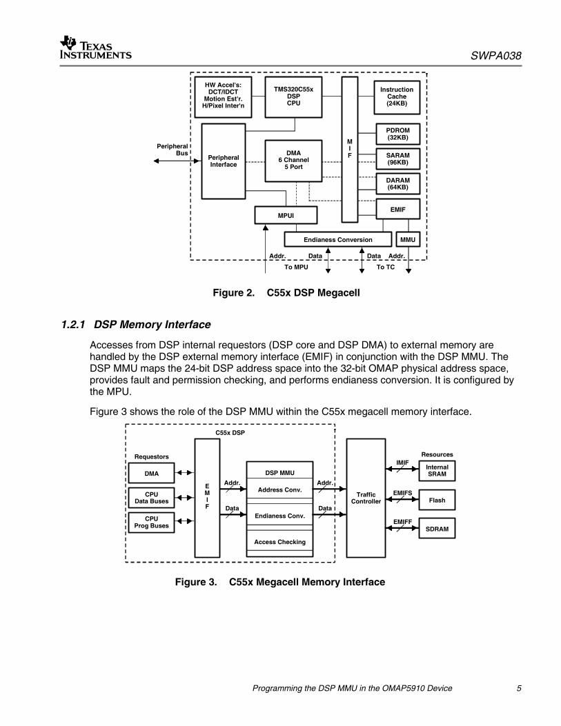
1.2 DSP Megacell Architecture
The DSP megacell consists of the C55x DSP core, the DSP internal memory, the DSP DMA, multimedia hardware accelerators, the instruction cache, and several interfaces to other OMAP™ units (see Figure 2).
Accesses from DSP internal requestors (DSP core and DSP DMA) to external memory are handled by the DSP external memory interface (EMIF) in conjunction with the DSP MMU. The DSP MMU maps the 24-bit DSP address space into the 32-bit OMAP physical address space, provides fault and permission checking, and performs endianess conversion. It is configured by the MPU.
Figure 3 shows the role of the DSP MMU within the C55x megacell memory interface.
Resources
DMA
CPUData Buses
CPUProg Buses
EMIF
DSP MMU
Address Conv.
Endianess Conv.
Access Checking
Addr.
Data
Addr.
Data
C55x DSP
IMIFInternalSRAM
Flash
SDRAM
EMIFS
EMIFF
Requestors
TrafficController
Figure 3. C55x Megacell Memory Interface
SWPA038
6 Programming the DSP MMU in the OMAP5910 Device
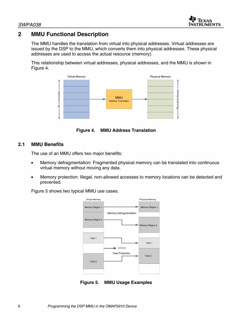
2 MMU Functional Description
The MMU handles the translation from virtual into physical addresses. Virtual addresses are issued by the DSP to the MMU, which converts them into physical addresses. These physical addresses are used to access the actual resource (memory).
This relationship between virtual addresses, physical addresses, and the MMU is shown in Figure 4.
MMUAddress Translation
Virtual Memory Physical Memory
Figure 4. MMU Address Translation
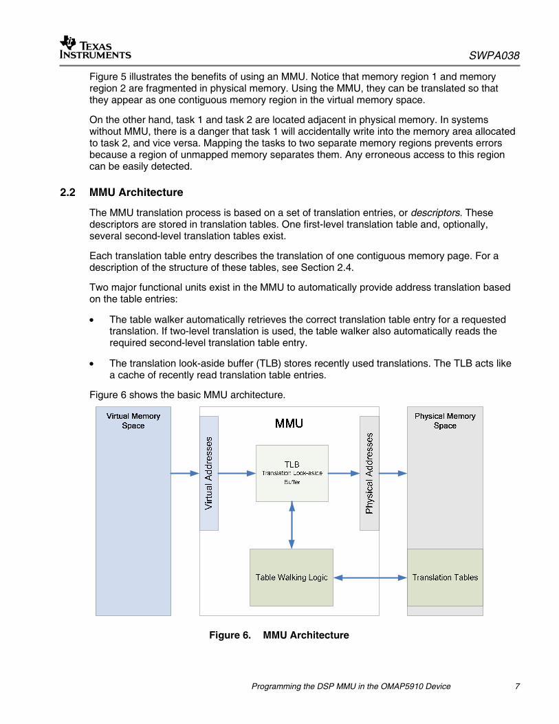
2.1 MMU Benefits
The use of an MMU offers two major benefits:
• Memory defragmentation: Fragmented physical memory can be translated into continuous virtual memory without moving any data.
• Memory protection: Illegal, non-allowed accesses to memory locations can be detected and prevented.
Figure 5 shows two typical MMU use cases.
Physical MemoryVirtual Memory
Memory Region 1
Memory Region 2
Task 1
Task 2
Memory Region 1
Memory Region 2
Task 1
Task 2
ERROR
Memory Defragmentation
Task Protection
Figure 5. MMU Usage Examples
SWPA038
Programming the DSP MMU in the OMAP5910 Device 7
Figure 5 illustrates the benefits of using an MMU. Notice that memory region 1 and memory region 2 are fragmented in physical memory. Using the MMU, they can be translated so that they appear as one contiguous memory region in the virtual memory space.
On the other hand, task 1 and task 2 are located adjacent in physical memory. In systems without MMU, there is a danger that task 1 will accidentally write into the memory area allocated to task 2, and vice versa. Mapping the tasks to two separate memory regions prevents errors because a region of unmapped memory separates them. Any erroneous access to this region can be easily detected.
2.2 MMU Architecture
The MMU translation process is based on a set of translation entries, or descriptors. These descriptors are stored in translation tables. One first-level translation table and, optionally, several second-level translation tables exist.
Each translation table entry describes the translation of one contiguous memory page. For a description of the structure of these tables, see Section 2.4.
Two major functional units exist in the MMU to automatically provide address translation based on the table entries:
• The table walker automatically retrieves the correct translation table entry for a requested translation. If two-level translation is used, the table walker also automatically reads the required second-level translation table entry.
• The translation look-aside buffer (TLB) stores recently used translations. The TLB acts like a cache of recently read translation table entries.
Figure 6 shows the basic MMU architecture.
Figure 6. MMU Architecture
SWPA038
8 Programming the DSP MMU in the OMAP5910 Device
2.3 MMU Address Translation Process
Whenever an address translation is requested (that is, for every memory access with the MMU enabled), the MMU checks first to see whether the TLB contains the requested translation.
As mentioned previously, the TLB acts like a cache, storing recent translations. It can also be manually programmed to ensure that time-critical data can be translated without delay.
If the requested translation is not in the TLB, the table walking logic retrieves the translation by reading the corresponding translation table entry/entries. After the logic has retrieved the correct translation, it updates the TLB and the address translation is performed. This process is summarized in Figure 7.
Figure 7. Translation Process
2.4 Translation Table Structure
The translation of virtual to physical addresses is based on entries in translation tables. These entries define the following properties:
• Address translation: Correspondence between virtual and physical addresses
• Access rights: Read and write, read-only, or no-access rights
• Size of the memory region this entry translates
The translation tables are indexed by the virtual address. Each virtual address corresponds to exactly one entry in a translation table. Conversely, each translation table entry describes the translation properties of a range of virtual addresses.
SWPA038
Programming the DSP MMU in the OMAP5910 Device 9
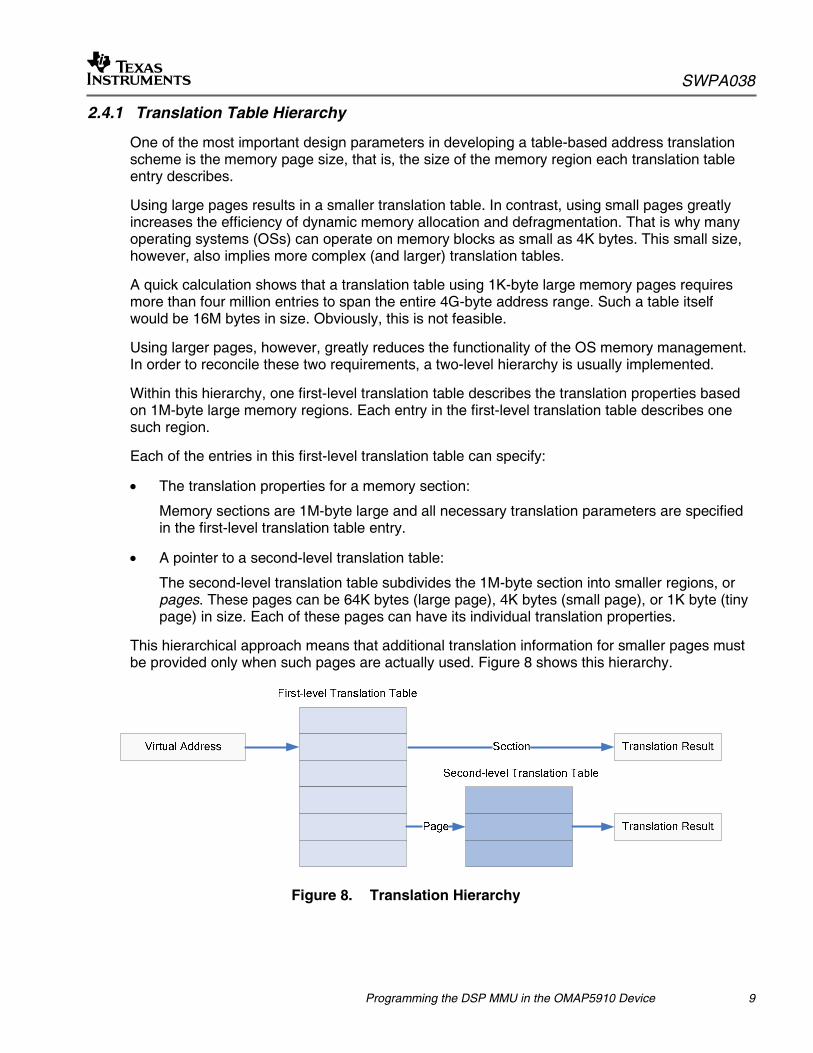
2.4.1 Translation Table Hierarchy
One of the most important design parameters in developing a table-based address translation scheme is the memory page size, that is, the size of the memory region each translation table entry describes.
Using large pages results in a smaller translation table. In contrast, using small pages greatly increases the efficiency of dynamic memory allocation and defragmentation. That is why many operating systems (OSs) can operate on memory blocks as small as 4K bytes. This small size, however, also implies more complex (and larger) translation tables.
A quick calculation shows that a translation table using 1K-byte large memory pages requires more than four million entries to span the entire 4G-byte address range. Such a table itself would be 16M bytes in size. Obviously, this is not feasible.
Using larger pages, however, greatly reduces the functionality of the OS memory management. In order to reconcile these two requirements, a two-level hierarchy is usually implemented.
Within this hierarchy, one first-level translation table describes the translation properties based on 1M-byte large memory regions. Each entry in the first-level translation table describes one such region.
Each of the entries in this first-level translation table can specify:
• The translation properties for a memory section:
Memory sections are 1M-byte large and all necessary translation parameters are specified in the first-level translation table entry.
• A pointer to a second-level translation table:
The second-level translation table subdivides the 1M-byte section into smaller regions, or pages. These pages can be 64K bytes (large page), 4K bytes (small page), or 1K byte (tiny page) in size. Each of these pages can have its individual translation properties.
This hierarchical approach means that additional translation information for smaller pages must be provided only when such pages are actually used. Figure 8 shows this hierarchy.
Figure 8. Translation Hierarchy
SWPA038
10 Programming the DSP MMU in the OMAP5910 Device
The structure of the first- and second-level translation tables and their entries is described in more detail in subsection 2.4.2 through subsection 2.4.4.3.
2.4.2 First-level Translation Table
The first-level translation table describes the translation properties based on sections of 1M byte. Sixteen 32-bit entries, or first-level descriptors, are required to describe the entire 16M-byte DSP virtual-address space.
The start address of the first-level translation table must be aligned on a 128-byte boundary; that is, at least the last seven address bits of the start address must be zero. This start address is called the translation table base and is a configurable parameter.
The table is indexed by the upper 4 bits of the virtual address. This mechanism is shown in Figure 9.
In summary, the translation table base and the translation table index together define the first-level descriptor address. Figure 10 outlines the mechanism used to calculate this address.
Each first-level descriptor provides either the complete address translation for a 1M-byte section or a pointer to a second-level translation table. Table 1 shows the first-level descriptor format.
Table 1. First-level Descriptor Format
First-level Descriptor Format
31:20 19:12 11:10 9:2 1 0
X 0 0 Fault
Coarse-page table base address X 0 1 Coarse page table
Section base address X AP X 1 0 Section
Fine-page table base address X 1 1 Fine page table
AP = Access permissions 0x = No access, 10 = Read-only access, 11 = Full access (read and write)
X = Don’t care
2.4.3.1 First-level Page Descriptor Format
If a translation granularity smaller than 1M byte is required, a two-level translation process is used. In this case, the first-level descriptor specifies only the start address of a second-level translation table used to allocate subsections, or pages, within the 1M-byte region the first-level descriptor describes.
The entries of the specified second-level translation table then define the translation properties of these pages. There are two types of second-level tables: coarse tables and fine tables. See subsection 2.4.4 for information on their differences.
2.4.3.2 First-level Section Descriptor Format
Each section descriptor in the first-level translation table specifies the complete translation properties for a 1M-byte memory section. Two parameters are defined by a section descriptor:
• Address translation: The physical start address of the section
• Access rights: No access, read-only, or read and write access
2.4.3.3 Section Translation Summary
Sections are translated based solely on the information provided by the first-level descriptor. Figure 11 summarizes the address translation process for a section.
SWPA038
12 Programming the DSP MMU in the OMAP5910 Device
Figure 11. Section Translation Summary
2.4.4 Two-level Translation
Two-level translation is used when a translation granularity smaller than 1M byte is required. In that case, the first-level descriptor provides a pointer to the base address of a second-level translation table.
Two types of second-level tables can be used:
• Coarse page tables with 256 entries:
Each entry in a coarse page table describes the translation properties of 4K bytes of memory.
• Fine page tables with 1024 entries:
Each entry in a fine page table describes the translation properties of 1K byte of memory.
The two least significant bits of the first-level descriptor indicate whether the second-level table is a coarse table or a fine table. The second-level table is indexed by bits 19:12 (coarse page table) or bits 19:10 (fine page table) of the virtual address. This indexing mechanism is shown in Figure 12.
SWPA038
Programming the DSP MMU in the OMAP5910 Device 13
First-level Translation Table
Firs
t-lev
el T
able
Inde
x
First-level Descriptor
Virtual Address23 19 020 12 (10) 11 (9)
Second-level Translation Table
Sec
ond-
leve
l Tab
le In
dex
Second-level Descriptor
Figure 12. Two-level Translation
Coarse table entries describe the translation of 1M bytes of address space in pages of 4K bytes (small page). They can also define the translation of a 64K-byte large page. In this case, the same descriptor must be repeated 16 times in the coarse page table.
Having large pages provides the advantage that they can be cached using only one entry in the translation look-aside buffer (TLB), even though they require 16 entries in the coarse page table.
Note that the start addresses of both coarse and fine tables must be aligned according to their respective size. This means that a coarse table with 256 entries of 4 bytes each must be aligned on a 1024-byte boundary; that is, the last 10 bits of its start address must be zero.
Similarly, a fine table with 1024 entries of 4 bytes each must be aligned on a 4096-byte boundary, that is, the last 12 bits of its start address must be zero.
2.4.4.1 Second-level Descriptor Format
Second-level descriptors provide all the necessary information for the translation of a large, small, or tiny page. In this, they are similar to first-level section descriptors. Table 2 shows the format of such a second-level descriptor.
Table 2. Second-level Descriptor Format
Second-level Descriptor Format
31:16 15:12 11 10 9 8:6 5:4 3:2 1 0
0 0 Fault
Large-page base address
X AP X 0 1 Large page
Small-page base address X AP 1 0 Small page
Tiny-page base address X AP 1 1 Tiny page
AP = Access permissions 0x = No access, 10= Read-only access, 11 = Full access (read and write)
X = Don’t care
SWPA038
14 Programming the DSP MMU in the OMAP5910 Device
2.4.4.2 Large- and Small-Page Translation Summary
The translation process for large and small pages using a second-level coarse page table is summarized in Figure 13. The numbers in parentheses refer to small pages.
Note that large descriptors must be repeated 16 times and that large pages must be aligned according to their size, which means that a large page always starts at a coarse table entry that is a multiple of 16.
First-level Translation Table
Firs
t-lev
el T
able
Inde
x
First-level Descriptor
Virtual Address23 19 020 16 (12) 15 (11)
Second-level (coarse)page table
Sec
ond-
leve
l Tab
le In
dex
Sec
ond-
leve
l D
escr
ipto
r
Physical Address31 15 (11) 016 (12)
Figure 13. Large- and Small-Page Translation Summary
2.4.4.3 Tiny-Page Translation Summary
The translation of tiny pages is defined by a fine page table. It contains 1024 entries, each describing the translation properties of 1K byte of memory.
NOTE: Most operating systems do not support such small allocation sizes; therefore, the support of 1K-byte memory pages will be discontinued in future OMAP generations.
Fine page tables are indexed using bits 19:10 of the virtual address. This is shown in Figure 14 .
SWPA038
Programming the DSP MMU in the OMAP5910 Device 15
First-level Translation Table
First-level Descriptor
Virtual Address23 19 020 10 9
Second-level (Fine)Translation Table
Physical Address31 9 010
Figure 14. Fine-Page Translation Summary
2.5 Translation Look-aside Buffer
Translating virtual to physical addresses is required for each memory access in systems using an MMU. In order to speed up this translation process, a cache mechanism (the TLB) has been introduced to store the results of recent translations.
For every translation request, the MMU internal logic checks first whether this translation already exists in the TLB. If it does, then this translation is used. Otherwise, the translation is retrieved from the translation tables, and the TLB is updated. If the TLB is full, one of the older entries must be replaced. The entry is selected randomly.
The first n TLB entries (with n < total number of TLB entries) can be protected, or locked, against being overwritten. This is done by setting the TLB base pointer to n (see Figure 15). The remaining entries are overwritten, if necessary, on a random basis. The victim pointer indicates the next TLB entry to be written.
Figure 15. TLB Entry Lock Mechanism
SWPA038
16 Programming the DSP MMU in the OMAP5910 Device
When table walking is enabled, TLB entries are automatically written by the table walking logic. Alternatively, entries can also be manually written by the user. This is done to ensure that the time-critical data accesses execute as fast as possible. Such user-defined entries are typically locked to prevent them from being overwritten subsequently.
2.5.1 TLB Entry Format
TLB entries consist of two parts:
• CAM part: Contains the virtual address tag used to locate the translation in the TLB. The TLB acts as a fully associative cache addressed by the virtual address tag. The CAM part also contains the entry type (section, pointer to coarse table, or pointer to fine table) and the preserved and valid flags.
• RAM part: Contains the address translation that belongs to the virtual address tag. It also contains the access permissions (no access, read-only access, and read and write access).
The valid parameter specifies whether an entry is valid or not. The preserved parameter determines the behavior of an entry in the event of a TLB flush. If an entry is set as preserved, it is not deleted upon a TLB flush. Such preserved entries must be deleted manually.
The TLB entry structure is shown in Figure 16.
Figure 16. TLB Entry Structure
3 Programming the DSP MMU
The DSP MMU can be programmed in two ways: by building translation tables or by writing all required entries directly into the TLB. A mix of these two ways is also possible. In that case, translation tables are used but some of the most time-critical translations are preloaded into the TLB.
SWPA038
Programming the DSP MMU in the OMAP5910 Device 17
3.1 Writing, Reading, and Deleting TLB Entries
For time-critical program routines, it is often desirable to ensure that the required MMU translations are always present in the TLB. This avoids the performance impact of retrieving these translations via a table walk.
It is therefore possible for the user to write some or all of the required translations manually into the TLB and to protect them against being overwritten. A maximum of 31 of the 32 TLB entries can be user-written and protected. One entry must always remain unprotected for use by the table walking logic.
The TLB entries can be read by the user to determine the currently buffered translations. Unused translations can be deleted.
3.1.1 Writing TLB Entries
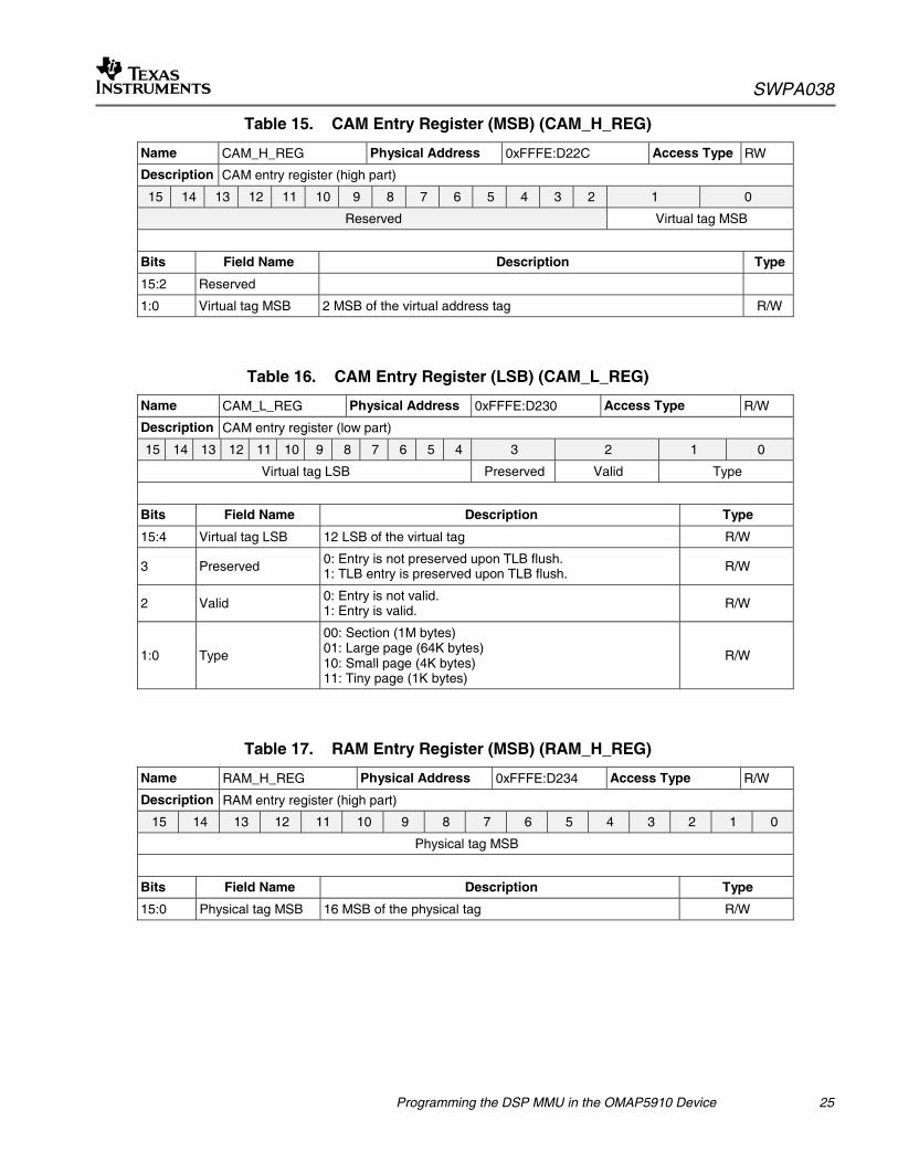
TLB entries are written using a set of configuration registers. Four registers (CAM_H_REG, CAM_L_REG, RAM_H_REG, and RAM_L_REG) are used to store the CAM and RAM parts of a TLB entry that will be written. The CAM and RAM parts are allocated in two registers (high and low) because they are bigger than 16 bits.
The CAM registers hold the virtual tag, that is, the 14 most significant bits of the virtual address. Additionally, they contain some status bits that define whether the entry is to be preserved upon a TLB flush operation, is valid or contains only random uninitialized content, and the type of memory block (section, large, small, or tiny page) this entry describes.
The RAM registers hold the physical address tag, that is, the 22 most significant bits of the physical address. Additionally, they define the access permissions of the memory region. Both the virtual and physical start addresses of sections and pages must be aligned according to their respective size.
This means, for instance, that for a 1M-byte section only address bits 23:20 (virtual) and 31:20 (physical) are significant.
In order to write a TLB entry, the user must first calculate the correct CAM and RAM parameters and place them into the corresponding CAM and RAM registers. Next, the lock register (LOCK_REG) is used to select (and, optionally, protect) the entry that will be written. Finally, the TLB entry is written to the specified location by setting the write TLB-entry bit in the LD_TLB_REG register.
A summary of all relevant TLB control registers is given in Section 4.
3.1.2 Protecting TLB Entries
The first n TLB entries (with n < total number of TLB entries) can be protected from being overwritten with new translations retrieved by the table walking logic. This is useful to ensure that certain (commonly used or time-critical) translations are always in the TLB and do not have to be retrieved via the table walking process.
The entry protection mechanism is shown in Figure 15 . To protect the first n TLB entries, set the base pointer field in the MMU lock register (LOCK_REG) to n, and set the current victim pointer (also in the MMU lock register) to a value greater than or equal to n.
SWPA038
18 Programming the DSP MMU in the OMAP5910 Device
3.1.3 Reading TLB Entries
Entries in the TLB can be read by using the victim pointer to specify the entry number. The parameters of this entry are then accessible in the CAM/RAM read registers (READ_CAM_H_REG, READ_CAM_L_REG, READ_RAM_H_REG, and READ_RAM_L_REG).
3.1.4 Deleting TLB Entries
Two mechanisms exist to delete TLB entries. All unpreserved TLB entries, that is, TLB entries that were written with the preserved bit set to zero, can be deleted by invoking a TLB flush. Such a flush is invoked by setting the flush bit in the TLB global flush register (GFLUSH_REG).
An individual TLB entry can be flushed, regardless of its preserved bit setting, by specifying its virtual address in the MMU CAM registers, and by setting the flush entry bit in the MMU flush entry register (FLUSH_ENTRY_REG).
The preserved bit should only be set for protected TLB entries, as it does not prevent replacement of the entry by the table walking logic.
3.1.5 Enabling the MMU
The MMU is enabled by setting the enable bit in the MMU control register (CNTL_REG). Clearing this bit disables the MMU. When the MMU is disabled, no translation is performed, meaning that virtual addresses are treated as physical addresses.
3.2 MMU Error Handling
The following types of faults can occur in the address translation process:
• TLB miss (table walker disabled):
No translation is found in the TLB for the virtual address issued. The hardware table walker is disabled, and hence the translation cannot be retrieved from the translation table(s).
• Translation fault (table walker enabled):
No translation is found for the virtual address required (TLB miss). The table walker is enabled, but no valid page table entry exists for the given virtual address.
• Permission fault:
The section/page access permissions do not match the access type.
When a fault occurs and its corresponding interrupt is enabled, an interrupt is signaled to the ARM. The interrupt service routine (ISR) is then responsible for fault recovery. For example, for a TLB miss, the ISR might load the missing entry from a page table. The DSP memory interface is stalled by the DSP MMU while the fault is handled.
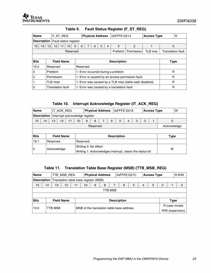
The ISR can determine the cause of the abort interrupt by reading the fault status register (F_ST_REG). The virtual address that caused the fault can be determined by reading the fault address registers (FAULT_AD_H_REG and FAULT_AD_L_REG).
SWPA038
Programming the DSP MMU in the OMAP5910 Device 19
In the case of a TLB miss, the MMU continues servicing the request as soon as a valid TLB entry has been written and the interrupt has been acknowledged via the acknowledge interrupt bit in the interrupt acknowledge register (IT_ACK_REG).
In the case of a permission fault, the corresponding TLB/translation table entry must be modified to allow for the requested access type before acknowledging the interrupt.
Figure 17 summarizes the MMU translation process and highlights the different error scenarios.
Figure 17. MMU Translation Process and Fault Types
SWPA038
20 Programming the DSP MMU in the OMAP5910 Device
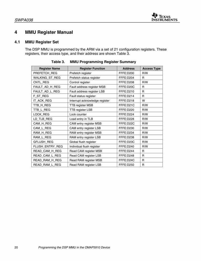
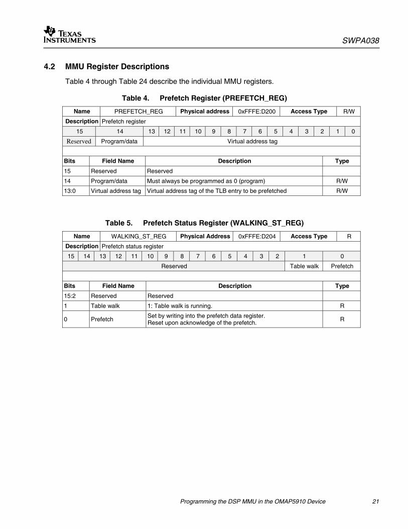
4 MMU Register Manual
4.1 MMU Register Set
The DSP MMU is programmed by the ARM via a set of 21 configuration registers. These registers, their access type, and their address are shown Table 3.
Table 3. MMU Programming Register Summary
Register Name Register Function Address Access Type
PREFETCH_REG Prefetch register FFFE:D200 R/W
WALKING_ST_REG Prefetch status register FFFE:D204 R
CNTL_REG Control register FFFE:D208 R/W
FAULT_AD_H_REG Fault address register MSB FFFE:D20C R
FAULT_AD_L_REG Fault address register LSB FFFE:D210 R
F_ST_REG Fault status register FFFE:D214 R
IT_ACK_REG Interrupt acknowledge register FFFE:D218 W
Name RAM_L_READ_REG Physical Address 0xFFFE:D250 Access Type R
Description Lock/protect entry register
15 14 13 12 11 10 9 8 7 6 5 4 3 2 1 0
Physical tag LSB Access permissions Reserved
Bits Field Name Description Type
15:10 Physical tag LSB 6 LSB of the physical tag R
9:8 Access permissions 00, 01: No access 10: Read-only access 11: Read and write access
R
7:0 Reserved
5 Conclusion
The OMAP5910 architecture provides a flexible way for the DSP to access external memory. The DSP memory management unit enables DSP access to the entire 32-bit OMAP physical address space. The address mapping between DSP and OMAP addresses is flexible and can be configured at run time to enable dynamic memory allocation. The DSP MMU implements memory protection, adding additional security against unauthorized memory accesses by the DSP.
6 References 1. OMAP5910 Dual-Core Processor Data Manual (SPRS197)
SWPA038
Programming the DSP MMU in the OMAP5910 Device 29
Appendix A. Demonstration Software
A.1 Example Projects
Two example projects are provided to demonstrate the DSP MMU setup. The first example shows how to configure the DSP MMU by writing the TLB entries directly. This is the most common use case.
The second example shows how to program the DSP MMU using a first-level translation table. For the sake of simplicity, no two-level translation process is demonstrated. Also, the focus of these projects is rather on demonstrating the steps required to program the DSP MMU than on providing the most efficient implementation.
The projects are written for the Code Composer Studio™ Integrated Development Environment (IDE) for OMAP, and the explanations assume that you are familiar with the Code Composer Studio™ IDE. The source code, on the other hand, is generic and can be ported easily to any other build/debug environment.
To use and debug these projects, extract the source code provided with this application note into a directory of your choice using a zip extraction utility.
A.2 Configuring the DSP MMU by Programming the TLB
The most common way to configure the DSP MMU is by writing the TLB entries directly without building translation tables. This is usually possible because the DSP has a comparatively small address space (16M bytes), and dynamic memory allocation via the MMU is not as common on the DSP as it is on the ARM.
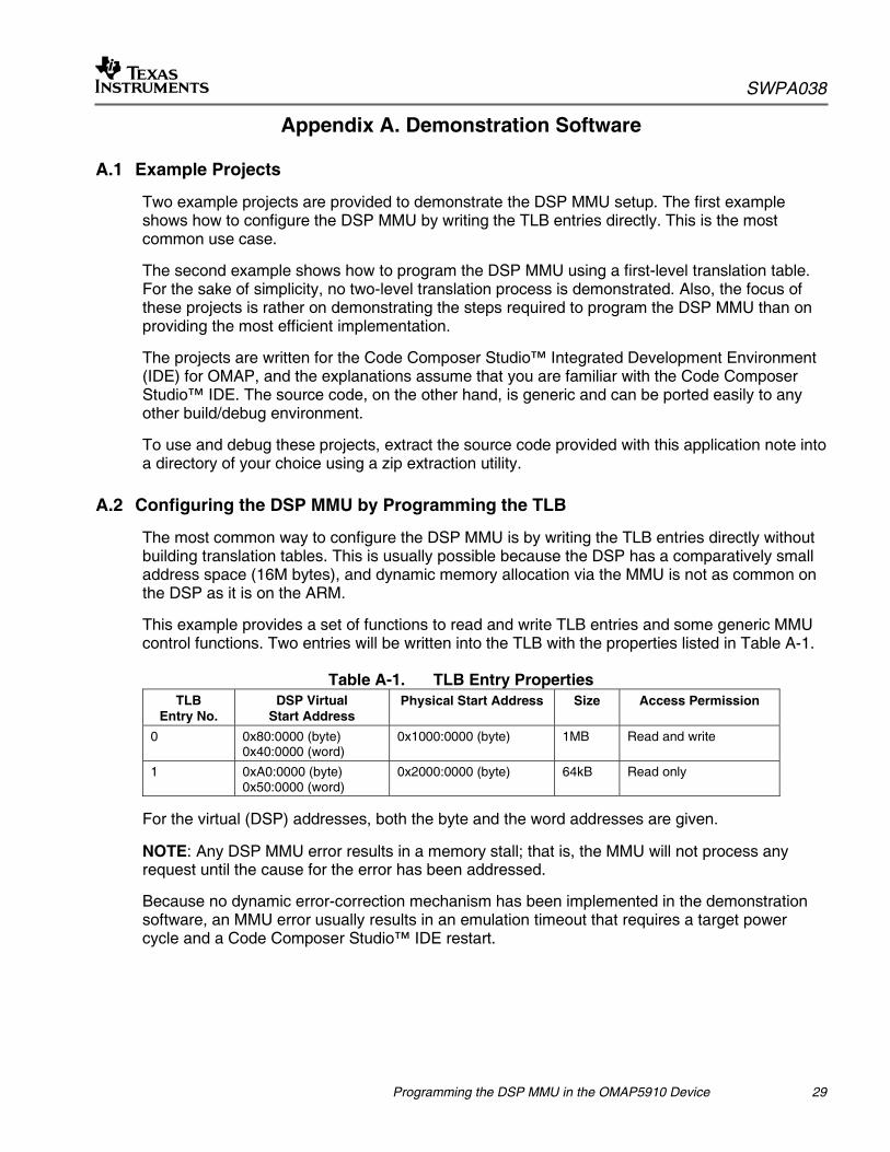
This example provides a set of functions to read and write TLB entries and some generic MMU control functions. Two entries will be written into the TLB with the properties listed in Table A-1.
For the virtual (DSP) addresses, both the byte and the word addresses are given.
NOTE: Any DSP MMU error results in a memory stall; that is, the MMU will not process any request until the cause for the error has been addressed.
Because no dynamic error-correction mechanism has been implemented in the demonstration software, an MMU error usually results in an emulation timeout that requires a target power cycle and a Code Composer Studio™ IDE restart.
SWPA038
30 Programming the DSP MMU in the OMAP5910 Device
A.2.1 Verification Procedure
To verify the program functionality:
1. Configure Code Composer Studio™ IDE for your target platform (OMAP1510, OMAP1610, OMAP1710, OMAP5910, or OMAP5912).
2. Start Code Composer Studio™ IDE, and open the ARM debugger window.
3. Open the project DSPMMU_TLB.pjt.
4. Load the program file DSPMMU_TLB.out from the \debug subdirectory.
5. Run the program. It configures the DSP MMU and then polls for possible error conditions.
6. Open a memory window in the ARM debugger at start address 0x10000000.
7. Open the DSP debugger.
8. Open a memory window to view data at address 0x400000. Make sure you set the page to DATA.
9. Compare the data values in both memory displays (ARM and DSP). They should be the same.
10. Change one data value in the DSP debugger (you can do this by double-clicking on it and writing the new value into the dialog box) and then refresh the memory window in the ARM debugger. The value changes there as well.
11. Verify the access permission functionality. Entry 1 in the TLB is configured as having only read permissions. Trying to write to its address space, therefore, results in a permission fault.
12. Change the start address of the DSP memory display to 0x500000. Try to write to a value there. This attempt results in an error message.
13. Check the ARM debugger. An access-permission error message displays in the stdout window.
14. Because the MMU does not process any request until the error cause has been addressed, you must now power cycle the processor and restart Code Composer Studio™ IDE. In typical user software, an error handling mechanism is included.
SWPA038
Programming the DSP MMU in the OMAP5910 Device 31
A.3 Configuring the DSP MMU by Building a Tanslation Table
Although configuring the DSP MMU by writing the TLB entries directly is more common, it is also possible to configure the DSP MMU by building translation tables, as the second example shows.
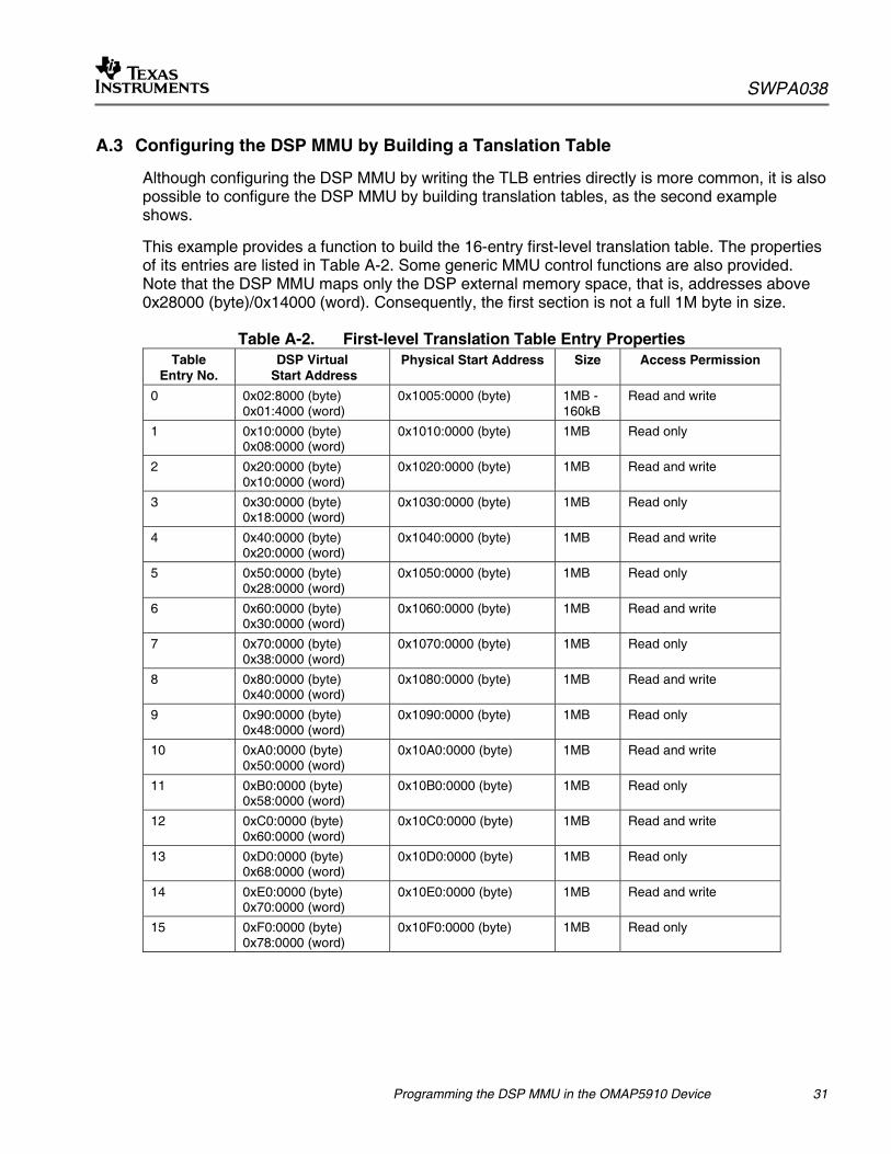
This example provides a function to build the 16-entry first-level translation table. The properties of its entries are listed in Table A-2. Some generic MMU control functions are also provided. Note that the DSP MMU maps only the DSP external memory space, that is, addresses above 0x28000 (byte)/0x14000 (word). Consequently, the first section is not a full 1M byte in size.
1. Configure Code Composer Studio™ IDE for your target platform (OMAP1510, OMAP1610, OMAP1710, OMAP5910, or OMAP5912).
2. Start Code Composer Studio™ IDE, and open the ARM debugger window.
3. Open the project DSPMMU_Table.pjt.
4. Load the program file DSPMMU_Table.out from the \debug subdirectory.
5. Run the program. It builds the first-level translation table used by the DSP MMU, configures the DSP MMU accordingly, and then polls for possible error conditions.
6. Open a memory window in the ARM debugger at start address 0x10200000.
7. Open the DSP debugger.
8. Open a memory window to view data at address 0x100000. Make sure you set the page to DATA.
9. Compare the data values in both memory displays (ARM and DSP). They should be the same.
10. Change one data value in the DSP debugger (you can do this by double-clicking on it and writing the new value into the dialog box), and then refresh the memory window in the ARM debugger. The value changes there as well.
11. Verify the access permission functionality. All odd entries in the first-level translation table (those corresponding to a start byte address with an odd most-significant digit) are configured as having only read permissions. Trying to write to its address space, therefore, results in a permission fault.
12. Change the start address of the DSP memory display to 0x180000. This corresponds to the physical address 0x10300000 in the ARM debugger. Try to change a value in the DSP memory display. This attempt results in an error message.
13. Check the ARM debugger. An access-permission error message displays in the stdout window.
14. Because the MMU does not process any request until the error cause has been addressed, you must power cycle the processor and restart Code Composer Studio™ IDE.
IMPORTANT NOTICE
Texas Instruments Incorporated and its subsidiaries (TI) reserve the right to make corrections, modifications,enhancements, improvements, and other changes to its products and services at any time and to discontinueany product or service without notice. Customers should obtain the latest relevant information before placingorders and should verify that such information is current and complete. All products are sold subject to TI’s termsand conditions of sale supplied at the time of order acknowledgment.
TI warrants performance of its hardware products to the specifications applicable at the time of sale inaccordance with TI’s standard warranty. Testing and other quality control techniques are used to the extent TIdeems necessary to support this warranty. Except where mandated by government requirements, testing of allparameters of each product is not necessarily performed.
TI assumes no liability for applications assistance or customer product design. Customers are responsible fortheir products and applications using TI components. To minimize the risks associated with customer productsand applications, customers should provide adequate design and operating safeguards.
TI does not warrant or represent that any license, either express or implied, is granted under any TI patent right,copyright, mask work right, or other TI intellectual property right relating to any combination, machine, or processin which TI products or services are used. Information published by TI regarding third-party products or servicesdoes not constitute a license from TI to use such products or services or a warranty or endorsement thereof.Use of such information may require a license from a third party under the patents or other intellectual propertyof the third party, or a license from TI under the patents or other intellectual property of TI.
Reproduction of information in TI data books or data sheets is permissible only if reproduction is withoutalteration and is accompanied by all associated warranties, conditions, limitations, and notices. Reproductionof this information with alteration is an unfair and deceptive business practice. TI is not responsible or liable forsuch altered documentation.
Resale of TI products or services with statements different from or beyond the parameters stated by TI for thatproduct or service voids all express and any implied warranties for the associated TI product or service andis an unfair and deceptive business practice. TI is not responsible or liable for any such statements.
Following are URLs where you can obtain information on other Texas Instruments products and applicationsolutions: