Project Number: BYK-BUG2 Laser Audio Surveillance Device A Major Qualifying Project Report submitted to the Faculty of WORCESTER POLYTECHNIC INSTITUTE in partial fulfillment of the requirements for the Degree of Bachelor of Science by ______________________ Vincent Amendolare ______________________ Wade Sarraf on December 19, 2005 Approved: Professor Brian King, Advisor
Transcript
Project Number: BYK-BUG2
Laser Audio Surveillance Device A Major Qualifying Project Report
submitted to the Faculty of WORCESTER POLYTECHNIC INSTITUTE in partial fulfillment of the requirements for the
Degree of Bachelor of Science by
______________________
Vincent Amendolare
______________________
Wade Sarraf
on
December 19, 2005
Approved:
Professor Brian King, Advisor
ii
Abstract
The purpose of this project was to create an eavesdropping device that operated
by pointing a laser beam at a window and reconstructing the audio of a conversation on
the other side of the window. The project sought to improve on a previous year’s project
which was sensitive to the angle between the laser beam and the window surface normal.
This system was implemented using a laser, arrangement of lenses, and circuitry
including a digital signal processor.
iii
Table of Contents Abstract ............................................................................................................................... ii Table of Contents............................................................................................................... iii Table of Figures .................................................................................................................. v Executive Summary .......................................................................................................... vii 1 Introduction................................................................................................................. 1 2 Project Objectives ....................................................................................................... 2
2.1 Project from Previous Year................................................................................. 2 2.2 Project Goals and Constraints............................................................................. 2
3 Background Information/Theory ................................................................................ 4 3.1 Acoustic Waves and Window Vibration............................................................. 4 3.2 Optical Theory .................................................................................................... 5
3.4.1 Correlation ................................................................................................ 15 3.4.2 Spectrometry and Doppler Effect ............................................................. 16 3.4.3 Time of Flight ........................................................................................... 17
4 Methodology............................................................................................................. 18 4.1 Investigation of Possible Implementation Methods.......................................... 18
4.1.1 Time of Flight ........................................................................................... 18 4.1.2 Doppler Shift............................................................................................. 19 4.1.3 Amplitude Modulation with Correlation .................................................. 19 4.1.4 Interferometry ........................................................................................... 20 4.1.5 Proof of Concept ....................................................................................... 20
4.2 Refinement of Design ....................................................................................... 21 4.2.1 Laser Diode Driver ................................................................................... 21 4.2.2 Optics ........................................................................................................ 22 4.2.3 Detection ................................................................................................... 22 4.2.4 Early Signal Processing ............................................................................ 23 4.2.5 Correlation ................................................................................................ 24 4.2.6 Digital Signal Processing.......................................................................... 25 4.2.7 Audio Driver ............................................................................................. 27 4.2.8 System Integration .................................................................................... 27
5.5 Total System Performance................................................................................ 68 6 Conclusions and Recommendations ......................................................................... 71
6.1 General Conclusions ......................................................................................... 71 6.2 Recommendations for Specific Modules .......................................................... 72 6.3 General Recommendations ............................................................................... 74
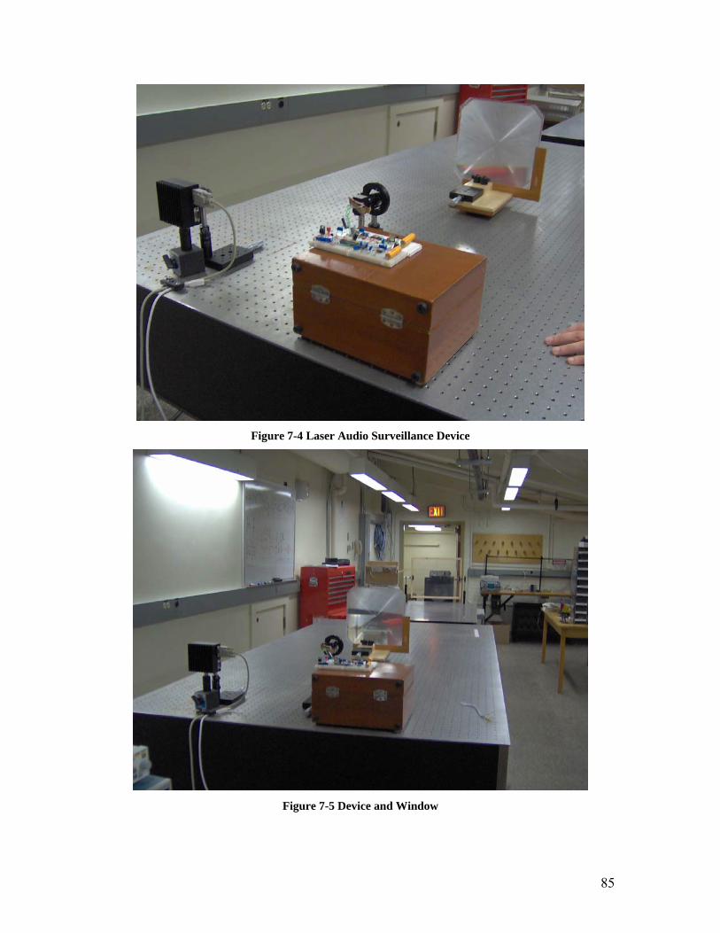
7 Appendices................................................................................................................ 76 7.1 Components List ............................................................................................... 76 7.2 Full Circuit Schematic ...................................................................................... 77 7.3 dsPIC Code ....................................................................................................... 78 7.4 System Pictures................................................................................................. 84
Table of Figures Figure 3-1 Divergence Angle.............................................................................................. 5 Figure 3-2 Convex Lens...................................................................................................... 6 Figure 3-3 LED Collimation............................................................................................... 6 Figure 3-4 Law of Reflection.............................................................................................. 7 Figure 3-5 Specular and Diffuse Reflection ....................................................................... 8 Figure 3-6 Angular Distribution of Light ........................................................................... 9 Figure 3-7 Acceptance Angle ........................................................................................... 11 Figure 3-8 Output Power vs. Forward Current of Laser Diode ........................................ 12 Figure 3-9 Interferometer.................................................................................................. 14 Figure 3-10 Fringe Pattern ................................................................................................ 15 Figure 3-11 Correlation Graph.......................................................................................... 16 Figure 0-1 System Block Diagram ................................................................................... 28 Figure 0-2 Laser Diode Driver Functionality ................................................................... 29 Figure 0-3 Laser Diode Driver Circuit.............................................................................. 30 Figure 0-4 Optics Functionality ........................................................................................ 32 Figure 0-5 Collimation Optics .......................................................................................... 32 Figure 0-6 Laser and Window Configuration (Side View) .............................................. 33 Figure 0-7 Laser and Detector Setup (Top View) ............................................................ 33 Figure 0-8 System Setup................................................................................................... 34 Figure 0-9 Detector Functionality.................................................................................... 34 Figure 0-10 Photo-Detector Circuit .................................................................................. 35 Figure 0-11 Theoretical Output of Detection Stage.......................................................... 36 Figure 0-12 Early Signal Processing Functionality .......................................................... 36 Figure 0-13 High Pass Filter Circuit................................................................................. 37 Figure 0-14 Theoretical High Pass Filter Output.............................................................. 37 Figure 0-15 Gain Stage ..................................................................................................... 38 Figure 0-16 Theoretical Output of Gain Stage ................................................................. 38 Figure 0-17 Clamper Circuit............................................................................................. 39 Figure 0-18 Theoretical Output of the Clamper Circuit ................................................... 39 Figure 0-19 Multiplier Functionality ................................................................................ 40 Figure 0-20 Analog Multiplier.......................................................................................... 40 Figure 0-21 Theoretical Output of Multiplier................................................................... 40 Figure 0-22 Integrator Functionality................................................................................. 41 Figure 0-23 Integrator with Reset Switch......................................................................... 41 Figure 0-24 Theoretical Output of Integrator ................................................................... 42 Figure 0-25 Digital Signal Processing Functionality........................................................ 43 Figure 0-26 dsPIC Pinout ................................................................................................. 44 Figure 0-27 dsPIC Circuit Diagram.................................................................................. 44 Figure 0-28 Program Functionality................................................................................... 46 Figure 0-29 Theoretical Output of Vpwm ........................................................................ 51 Figure 0-30 Reconstruction Filter..................................................................................... 52 Figure 0-31 Full Circuit Schematic................................................................................... 53 Figure 5-1Voltage across Laser Diode ............................................................................. 55 Figure 5-2 Detector Stage output Voltage (No Capacitor) ............................................... 56
vi
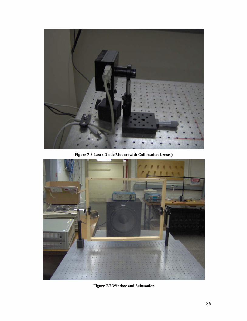
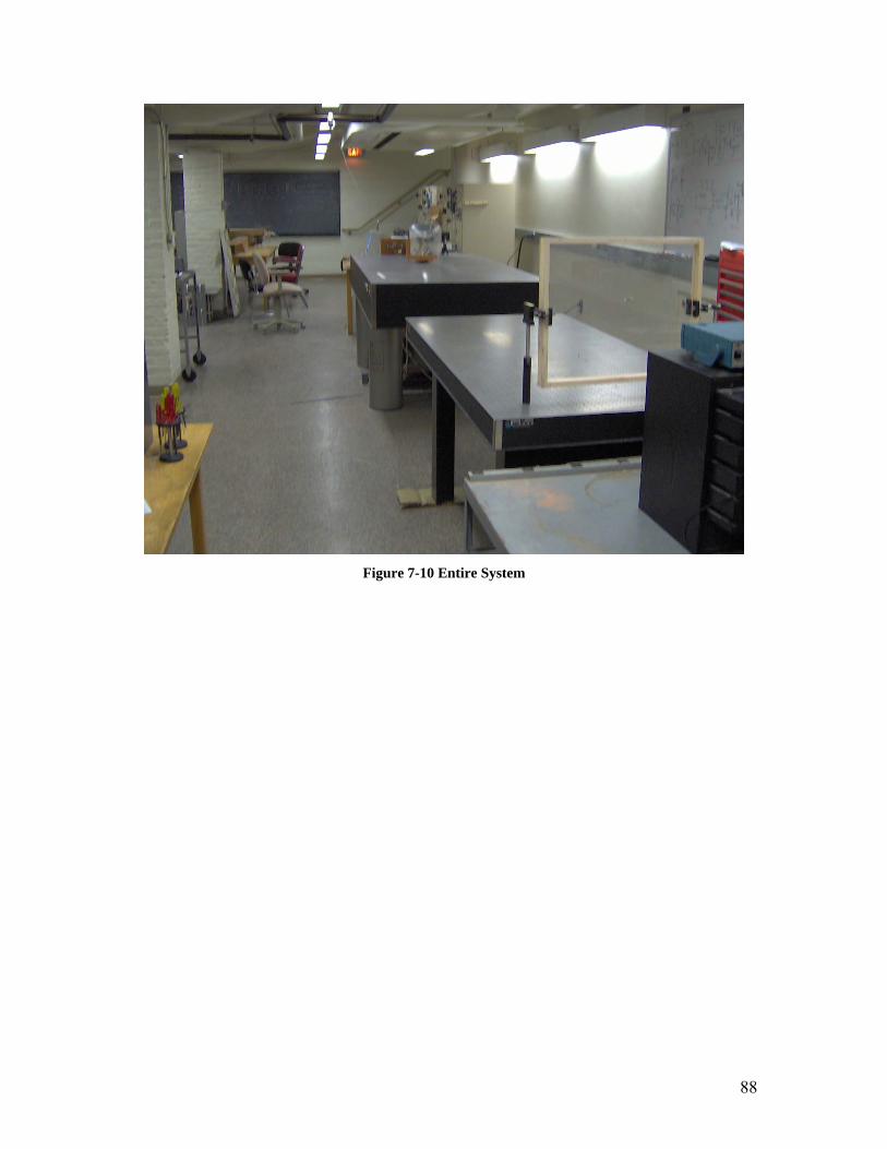
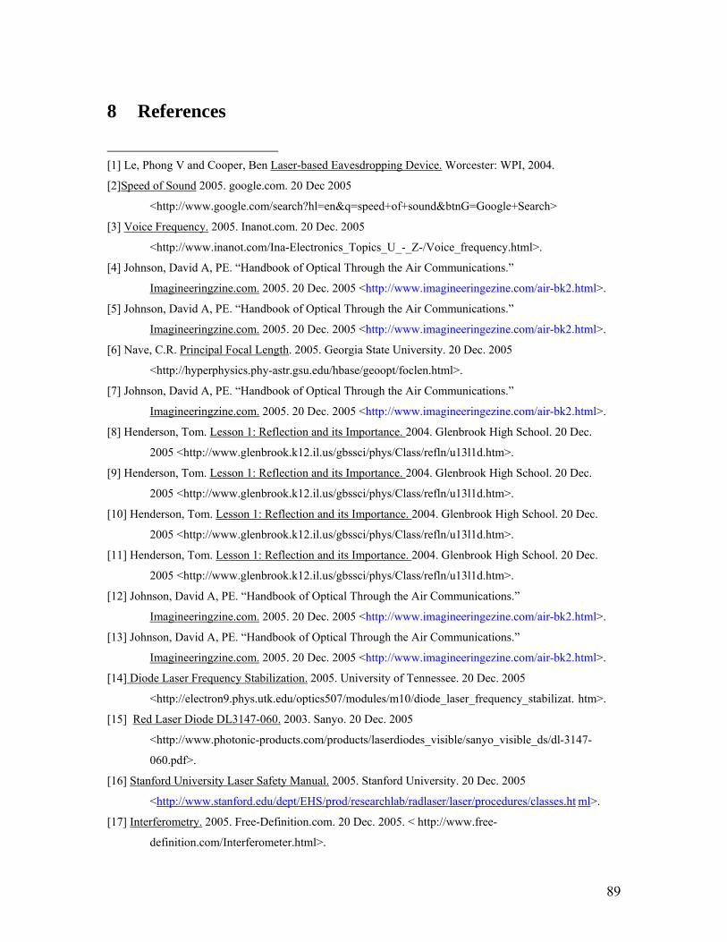
Figure 5-3 Detector Stage output Voltage (With Capacitor) ............................................ 57 Figure 5-4 High Pass Filter Stage Output ......................................................................... 58 Figure 5-5 Gain Stage Output ........................................................................................... 59 Figure 5-6 Output of Clamper Stage................................................................................. 60 Figure 5-7 Multiplier Output ............................................................................................ 61 Figure 5-8 Integrator Output............................................................................................. 62 Figure 5-9 Inverted and Non-Inverted Clock Outputs...................................................... 63 Figure 5-10 Clock Outputs with Interrupt ........................................................................ 64 Figure 5-11 Vreset Waveform .......................................................................................... 65 Figure 5-12 Output of PWM with Sinusoidal Input ......................................................... 66 Figure 5-13 PWM Output and Reconstructed Signal ....................................................... 67 Figure 5-14 Input Waveform and Reconstructed Signal .................................................. 68 Figure 5-15 Total System Setup ....................................................................................... 69 Figure 5-16 Reconstructed Audio Signal.......................................................................... 70 Figure 7-1 Full Circuit Schematic..................................................................................... 77 Figure 7-2 Circuit Picture ................................................................................................. 84 Figure 7-3 Circuit and Detector Assembly Picture........................................................... 84 Figure 7-4 Laser Audio Surveillance Device.................................................................... 85 Figure 7-5 Device and Window........................................................................................ 85 Figure 7-6 Laser Diode Mount (with Collimation Lenses) .............................................. 86 Figure 7-7 Window and Subwoofer.................................................................................. 86 Figure 7-8 Fresnel Lens .................................................................................................... 87 Figure 7-9 Detector Assembly and Additional Lens ........................................................ 87 Figure 7-10 Entire System ................................................................................................ 88
vii
Executive Summary The purpose of this project was to design a remote audio surveillance device. This
project was a follow-up to a Major Qualifying Project (MQP) completed the previous
academic year, which created a remote audio surveillance device that used a laser beam
incident on a window to listen to a conversation. Their device was successful in
achieving their goal, but not without significant limitations. These limitations included
that fact that their device needed to be very carefully set up knowing precisely where the
laser beam and the laser beam reflected from the window. Their device was also
extremely sensitive to external vibrations. These limitations are not very desirable in a
situation where one desires to eavesdrop on a conversation. Their device required the
measurement of the reflected laser beam, which essentially meant that they needed to
point the laser perpendicular to the window so that the reflected beam would come
straight back. This would not be practical in many situations.
We strove to design a device that used the same principle of shining a laser beam
on a window to eavesdrop on a conversation, but to overcome the limitations that
hindered the previous project. Our main focus was to create a device that could simply be
pointed at a window, without any concern for the location of the reflected beam, and still
listen to the conversation within the window
The basic physical principle exploited in the previous year’s project was that
when an acoustic wave is incident on a window it causes the window to bow in and out
slightly. This causes the angle of the surface of the window to change slightly, changing
the angle of reflection of any reflected light. Since the reflected light from a laser on a
window is not uniform, the amplitude of light measured at any given point will change if
the angle of the window changes. The previous year’s project used two light detectors to
measure the deviation in position of a reflected laser beam. In order to make any
measurements without knowing the position of the reflected beam we needed to measure
light that was being reflected back towards the device.
When a laser is incident on a window, most of the light will be reflected back in
the form of a beam, however some of the light is scattered back in all directions, known
as backscatter. If our device was to perform the function we intended it to, it needed to be
able to detect these very small levels of light and extract the audio information from it.
viii
Thus the main focus of this project was to design a device that could measure
extremely small amounts of light, and also be able to discard any light information from
any source but the laser. In order to perform this task we needed to create a system that
used various techniques to work with the very small signal we were able to detect. We
used a technique known as “Walsh Function Correlation” to be able to extract the small
signal from the noise present in the circuit. We also used a digital signal microprocessor
to provide us with digital signals needed as well as process our audio signal so it could be
then converted back into audio.
Unfortunately, due to time constraints we were unable to bring our system to the
level of functionality desired. Ultimately we were not able to extract audio information
from the small levels of light we could detect. We were able to detect relatively small
amounts of light with the system; we could tell whether or not backscatter was present.
We were able to prove the functionality of our system by using the actual reflected laser
beam. Our goal was to create a device that did not require the use of the reflected laser
beam, however we used it to test the system and indeed were able to detect audio with
this much stronger signal.
Although we did not meet the objectives of the project that we set for ourselves,
we did make major accomplishments towards reaching this goal. Based upon the results
of our project, we conclude that our goals are possible to attain and with further time
invested into another design phase, we believe a successful device could be implemented.
We therefore recommend to our advisor that he consider assigning a future MQP group
the task of using the research and design work we have put towards reaching this goal.
1
1 Introduction The purpose of this project was to create a remote audio surveillance device. Such a
device would allow the user to listen to a remote conversation without ever having to
infiltrate the premises. This project was the second design phase in building such a device.
During the previous academic year an initial attempt to build such a device was completed
by another project group. Our objective was to improve on their design.
Acoustic waves created by the human voice cause a nearby window to vibrate on a
very small scale. By shining a laser beam on a window and analyzing the reflected beam, it
is possible to retrieve the audio information from a conversation near the window. The
vibration of the window will actually cause the window to bow in and out slightly,
changing the angle at each point in the window along with the audio signal. If a laser beam
was incident on this window, the angle that the reflected beam would come back at would
vary with this angular change. By determining how much the reflected laser beam was
displaced, the audio signal could then be recreated. The previous project team implemented
such a device successfully.
Their device had significant limitations however. Their testing showed that their
device was extremely sensitive to external vibrations. Also their device needed to be
carefully set up with a photo-detector assembly placed precisely where the reflected beam
was. This generally meant that unless one could place the detector far away from the laser
itself, then the laser beam had to be approximately perpendicular to the window, limiting
the possible locations from which to plant the device. These were the main two limitations
of the previous team’s design, and were the areas in which we tried to improve the device.
Our objective was to use backscatter, the small amount of light reflected diffusely
from the window, to be able to recover the audio signal from a wider range of angles, and
without needing to carefully place a detector assembly. We also sought to make our device
less sensitive to external vibrations. In order to be able to detect the very small amount of
light reflected as backscatter, we needed to create a system that was extremely sensitive to
light, and also could differentiate the component of light that was being reflected from the
window as opposed to the ambient light. In this report we will explain the avenues we
explored to create such a device, and the degree to which it was a success.
2
2 Project Objectives Our project is the second phase of design of a laser audio surveillance device. We
based our goals for this project on the success and limitations of the previous instance of
this project. The scope of our project was also limited by other parameters such as time
and resources. In this section we will explain how we formulated our project objectives
based upon these factors.
2.1 Project from Previous Year In the 2004-2005 academic year, a Major Qualifying Project was completed to
build a laser audio surveillance device to eavesdrop on conversations by pointing a laser
beam at a window. As mentioned, acoustic waves cause the angle of a window pane to
change with an incident acoustic wave.
The students who completed this project last year utilized this principle. They
pointed a laser beam at a window and carefully placed their detector assembly to
intercept the reflected beam. This detector assembly had two photo-detectors placed some
distance apart with the reflected beam in the between them when the window was at rest.
When the window began to vibrate, the beam’s position moved and became closer to one
detector. The relative intensities that each detector observed made it possible to
determine the beams position, and thus the angle at which it was being reflected.
This method proved to be successful for observing conversations by pointing a
laser beam at a window. The main limitation to this approach however, was the extreme
sensitivity of the placement of the detector assembly. The detector assembly needed to be
carefully placed making the device more difficult and time consuming to set up. Also,
unless one desired to place the detector assembly far away from the laser, then the laser
beam needed to be approximately perpendicular to the window, limiting the possibilities
of placement points for the device. In addition, the device was also extremely sensitive to
any external vibrations that would vibrate the laser or detector assembly, causing noise in
the detected audio signal. [1]
2.2 Project Goals and Constraints The primary goal of this project was to create a laser audio surveillance device
that improved upon the previous year’s design in its main areas of limitation: ease of
3
setup and sensitivity to external vibration. We sought to create a device which would
work without having to carefully set up a detector in a reflected laser beam, but rather a
device which would work simply by pointing a laser at a window, with no dependence on
the location of the reflected beam. We realized that it may not be possible to use our
device at all angles of incidence with the window, but we sought to achieve the widest
range of angles possible. This device needed to be used remotely and therefore function
at significant distances from the window.
This project was completed in 14-weeks, time was a major constraint to what was
possible for us to accomplish. Also we were limited to a $250 budget. We were provided
an optics laboratory with both electrical and optical equipment necessary for the project.
Further practical constraints existed for the device itself. We sought to create this
device using a low power laser to avoid any safety concerns. We decided that the device
should be portable and therefore run on batteries. We also took into consideration
temperature fluctuations so they would not adversely affect the device.
4
3 Background Information/Theory
In this section we will explain the background information and theory necessary
to understand the functionality of our project discussed later in the report. Pertinent topics
include: optics, lasers, vibration, and light detection.
3.1 Acoustic Waves and Window Vibration
What humans perceive as sound is acoustic waves traveling through the air. These
are pressure waves; the pressure of the air varies as a function of space in a wave pattern
and these waves propagate through the air at the speed of sound (340 m/s) [2]. These
wave patterns are created by any vibrating objects which cause disturbances in the air
pressure, which is an acoustic wave. Humans can hear acoustic waves as sound from
approximately 20Hz to 20kHz, while human voices produce sound from about 300Hz to
3400Hz [3].
Acoustic waves are not only caused by objects vibrating but can also cause
objects to vibrate. For example, a speaker vibrating can create an acoustic wave while
another speaker can be caused to vibrate by this acoustic wave and act as a microphone.
This same principle applies to a window. An acoustic wave hitting the window will cause
it to vibrate, if only a very small amount. Generally the sides of a window are firmly
fixed so most of the vibration occurs towards the center of the window. This causes the
window to bow in and out with the vibrations. The window will actually vibrate in
several two dimensional mode patterns. At a given point on a window however, vibration
will be present from most or all of the vibrating modes, containing all of the audio
information.
The fundamental principle about the window’s vibration that the detection method
utilized was that this bowing action causes the angle of the glass to change slightly. This
means that if a light source was incident on the window, the reflected light would change
in angle as the window surface changed in angle from the acoustic waves.
5
3.2 Optical Theory
Laser light is the medium which the previous project team used to obtain audio
information from a vibrating window. Electronic circuits ultimately processed the
information carried by the laser into a convert it back into sound for an eavesdropper to
listen to. Assuming we would use a similar approach, research into the area of optics was
necessary. In this section we will present background information on optics relative to the
system we designed.
3.2.1 Collimation Concepts
The first stage in the most laser systems is the collimation of the light source.
When laser light leaves the source with no optics it radiates out in a predetermined
pattern. The angle over which the light will spread after it leaves the sources is defined as
the divergence angle. The most common definition of the divergence angle is the half-
angle between the center of the beam and the half power point on either side [4].
[5] Figure 3-1 Divergence Angle
The goal of collimation is to make the divergence angle zero, in other words the
photons of light leaving the collimation lens will all be moving in the same direction and
not spread out. In reality perfect collimation can never be achieved due to imperfections
of lens alignment and the diffraction of light.
To achieve collimation generally convex lenses are used. The effectiveness of
collimation is dependent on the radius, and focal length of the collimation lens as well as
the divergence angle of the light source. A convex lens, as shown in the figure below
directs the parallel beams coming from the left to a point to the right of the lens. This
point is called the focal point, and the distance it is away from the lens is called the focal
length of the lens.
6
[6] Figure 3-2 Convex Lens
Now consider the effect of light that is being radiated from a source at the focal
point of the lens. If you look at the figure above you can see that all the light generated
from a source at the focal point is directed in parallel beams moving to the left. The
beam has been collimated. Of course this case is ideal, light from a source at the focal
length diverges just enough to reaches to hit the outer edge of the lens.
[7] Figure 3-3 LED Collimation
The figure above illustrates less then ideal scenarios. If the light diverges past the outer
edge of the lens you are losing light that could have been collimated. If the light does not
reach the outer edge the lens you are using is too large and could be replaced with a
smaller cheaper lens. The third example is the correct setup for collimation.
3.2.2 Transmission and Reflection Concepts The transmission and reflection of light are also important concepts relevant to
this project. The main concepts that govern this process are the Fresnel equation, the
inverse square law, and the principles of reflection.
When a laser beam is incident on a window some of it will pass through and some
will be reflected back. The equation that governs the ratio between the reflected and
7
passed amounts of the beam is the Fresnel equation. The equation predicts the reflected
and passed percentages based on the refractive index of air versus the glass. The
approximate estimate for reflection percentage of a laser reflecting off glass is around
4%; the rest passes through the glass.
The fraction of the beam that gets reflected back follows the laws of reflection.
The Law of Reflection governs the behavior of light as it bounces off of a reflective
surface. The elements of a reflection include an incoming ray of light (the incident ray),
the normal line, and the reflected ray. The normal line is drawn perpendicular to the
surface at the point of incidence. The law states that the angle of the incident ray with
respect to the normal line will equal the angle of the reflected ray with respect to the
normal line[8].
[9] Figure 3-4 Law of Reflection
We cannot assume that a window’s surface is perfectly smooth. Under some level
of magnification the window will appear to have imperfections. The properties of a
surface on the microscopic level determine the behavior of incident light beams. The two
extremes of reflection are diffuse and specular reflection [10].
Diffuse reflection is the result of a beam of light hitting a surface that is rough
with respect to the light’s wavelength. This means that the deviations in the surface are
similar in magnitude to the wavelength of the incident light. The reflected light rays all
follow the Law of Reflection but because the surface orientation is changing, the light is
being reflected back in different directions. The right diagram in the figure below depicts
a diffuse reflection.
8
[11] Figure 3-5 Specular and Diffuse Reflection
Specular Reflection is the result of light beam reflecting off a surface that is
smooth with respect to the wavelength of the incident light. In the case of light, a mirror
or anything else of similar smoothness causes specular reflection. As illustrated in the left
diagram of the above figure, all of the incident light is reflected in the same manner
because the orientation of the surface remains constant with respect to the beam.
In the case of a laser beam being reflected off of a window, the reflected light will
have components of both specular and diffuse reflection. The specular reflection forms
the reflected beam, while the diffuse reflection is known as backscatter.
If an observer witnessed a laser beam incident on a window, they would see a
faint dot on the window at the spot where the laser hits the window. What they see would
be the light that is diffusely reflected from the window at that point, some of which
travels in the direction of the witness’ eye. This dot on the window is known as the
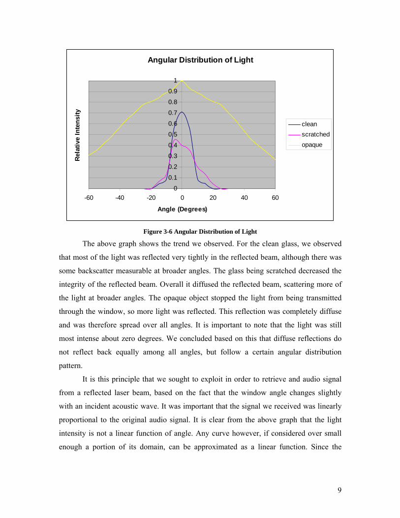
backscatter dot. We conducted an experiment to determine the angular distribution of
light reflected off of a window surface. We measured the angular distribution of light
with a laser incident on a clean window, scratched window, and an opaque spot on the
window (paper).
9
Angular Distribution of Light
0
0.1
0.2
0.3
0.4
0.5
0.6
0.7
0.8
0.9
1
-60 -40 -20 0 20 40 60
Angle (Degrees)
Rela
tive
Inte
nsity
cleanscratchedopaque
Figure 3-6 Angular Distribution of Light
The above graph shows the trend we observed. For the clean glass, we observed
that most of the light was reflected very tightly in the reflected beam, although there was
some backscatter measurable at broader angles. The glass being scratched decreased the
integrity of the reflected beam. Overall it diffused the reflected beam, scattering more of
the light at broader angles. The opaque object stopped the light from being transmitted
through the window, so more light was reflected. This reflection was completely diffuse
and was therefore spread over all angles. It is important to note that the light was still
most intense about zero degrees. We concluded based on this that diffuse reflections do
not reflect back equally among all angles, but follow a certain angular distribution
pattern.
It is this principle that we sought to exploit in order to retrieve and audio signal
from a reflected laser beam, based on the fact that the window angle changes slightly
with an incident acoustic wave. It was important that the signal we received was linearly
proportional to the original audio signal. It is clear from the above graph that the light
intensity is not a linear function of angle. Any curve however, if considered over small
enough a portion of its domain, can be approximated as a linear function. Since the
10
changes in angle the window undergoes are extremely small, we hypothesized that the
reflected light intensity would behave as a linear function of the incident acoustic wave.
3.2.3 Detection Concepts Once the light reflects off the window it immediately has some angular
distribution. The rate that this distribution spreads out as function of distance from the
source is governed by the Inverse Square Law. In terms of light the Inverse Square Law
states that the intensity I, of the light a distance D, away from the source will be the
sources intensity times the inverse of the square of the distance, that is I *D-2.
As an example let us consider attempting to detect laser light at a distance of
about 20 ft from the window. According to the Inverse Square Law the intensity of the
light reflected will be 0.0025. If the reflection off the window were completely diffuse
and 100% of the beam was reflected then the intensity of light at 20ft would be ¼ of a
percent. This is the best case scenario, the reality is that the window appears smooth at
the wavelength of laser and a good portion of the light is reflected in a specular manner.
It is difficult to determine the exact amount of backscatter but consider the
scenario where the window is slightly flawed so 5% of the beam is reflected, and 10% of
the reflection is diffuse. That means that the percentage of the main beam that we would
be able to detect right at the window would be ½ of a percent. 20ft away from the
window the intensity would be 0.00125%.
Integrating the amount of light on a half sphere 20ft away from the window would
add up to the original amount reflected light. The optics setup on the detection end of the
circuit determines how much of this light the detector will receive. The ratio of the
surface area of the detector lens to the surface area of the sphere is the fraction of the total
reflected light that the detector can see.
11
The detection lens must also have an acceptance angle allows it to observe the
reflected light.
[12] Figure 3-7 Acceptance Angle
The half-angle over which the receivers lens can focus light onto the receiver is defined
as the acceptance angle[13]. All light outside of this cone will not be measured by the
detector.
3.3 Lasers
A laser is a source of light with several properties which make them unique
compared to most sources of light. Lasers are monochromatic, coherent and highly
directional. These properties make lasers extremely useful as these properties can be
exploited to achieve many useful results.
The fact that a laser is monochromatic means that it only releases light of a single
frequency/wavelength. It is more correct to say that lasers produce light that is very
tightly centered around one frequency; more so than any other light source. Lasers are
available in a broad range of frequencies, from far-infrared through the visible light
spectrum to ultraviolet light. The frequency which a laser operates at can fluctuate with
temperature and also the injection current. There are various methods employed to
counteract these problems in applications where the stability of the frequency is
important. [14]
Coherent light is light in which each photon travels in step with the other photons.
This results in the light having a specific phase at a given point since each wave front
travels in unison. This can be useful when laser light from two paths is superimposed and
a wave interference pattern is created. This can be used to tell the difference in distance
of the two light paths with a technique called interferometry.
Laser light is emitted with its light traveling in a specific direction. This means
that laser light can travel over relatively great distances in a tightly focused beam
12
compared to other sources of light. This is useful when it is desired to send light to a
specific point over a significant distance.
One important technique that can be used with lasers, as well as other light
sources, is amplitude modulation. The amplitude of the laser light is changed with time to
correspond to a given function. If a detector is then used to detect the laser light, the
function can be looked for in the detected signal to determine the contribution from the
laser light as opposed to stray ambient light. The other advantage to amplitude
modulation is that it moves any information it is carrying from its original bandwidth (for
example the audio band) up to around its carrier frequency. This is useful because it may
be easier to transmit these higher frequencies, or to isolate the desired information
through filtering. Lasers can generally be modulated much faster than other light sources
which are another reason they are useful.
There are many different types of lasers. They vary in terms of cost, size,
frequency, beam shape, power and are used for a wide range of applications. One of the
most common types of laser for low-power inexpensive applications is the laser diode. In
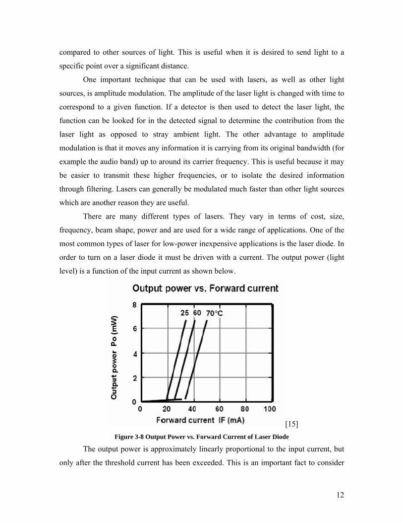
order to turn on a laser diode it must be driven with a current. The output power (light
level) is a function of the input current as shown below.
[15] Figure 3-8 Output Power vs. Forward Current of Laser Diode
The output power is approximately linearly proportional to the input current, but
only after the threshold current has been exceeded. This is an important fact to consider
13
when modulating the laser diode. One must be sure that the input current never goes
below the threshold value or the laser will turn off, and take a few microseconds to turn
back on, which is undesirable. It is also important to note that any fluctuation in the input
current may cause an undesired fluctuation in the output power. Temperature may also
cause the power curve to be shifted, as seen in the above figure. These problems can be
alleviated by control systems that use a photo-detector to ensure that the output power is
constant.
The output power level of a laser is a concern due to lasers being a safety hazard.
Lasers have been given classifications based on their output power for this reason. A
qualitative description of these classes is given below:
Class 1 lasers
Class 1 lasers are considered to be incapable of producing damaging radiation levels, and are therefore exempt from most control measures or other forms of surveillance. Example: laser printers.
Class 2 lasers
Class 2 lasers emit radiation in the visible portion of the spectrum, and protection is normally afforded by the normal human aversion response (blink reflex) to bright radiant sources. They may be hazardous if viewed directly for extended periods of time. Example: laser pointers.
Class 3 lasers
Class 3a lasers are those that normally would not produce injury if viewed only momentarily with the unaided eye. They may present a hazard if viewed using collecting optics, e.g., telescopes, microscopes, or binoculars. Example: HeNe lasers above 1 milliwatt but not exceeding 5 milliwatts radiant power.
Class 3b lasers can cause severe eye injuries if beams are viewed directly or specular reflections are viewed. A Class 3 laser is not normally a fire hazard. Example: visible HeNe lasers above 5 milliwatts but not exceeding 500 milliwatts radiant power.
Class 4 lasers
Class 4 lasers are a hazard to the eye from the direct beam and specular reflections and sometimes even from diffuse reflections. Class 4 lasers can also start fires and can damage skin. [16]
The output power of a laser is important to consider in any laser application.
3.4 Sensing methods
Now that we have discussed these optical principles and the functionality of
lasers, we can begin examining methods of light detection. Our specific project goal has
never been attempted as far as we know, so we will need to decide what the most logical
14
method of measuring light is for us. The possible methods we have come up with are
adaptations of techniques used to either capture very small signals in general, and/or
previously used to measure distance. In this section we will give some background
information on Interferometry, Correlation, Spectrometry, and Time of Flight techniques.
For our purposes, interferometry is a method involving the combination of two or
more optical measurements, and combining these data to form a greater picture based on
the combination of the two sources. [17] This methods works on the principal that waves
arriving at the same time will interfere with each other. Constructive interference is when
waves arrive in phase with each of other, in which case their amplitudes add. Destructive
interference is when waves arrive out of phase, the parts of the wave that are of opposite
sign will subtract. The worst case is when the waves are 180 degrees out of phase and the
waves cancel each other out.
[18] Figure 3-9 Interferometer
The above figure shows the setup of a Michelson Interferometer. Laser light,
which is coherent and monochromatic, is projected upon a half silvered mirror which
passes half the beam through and reflects the rest at a 45 degree angle. The laser beams
then bounce off their respective mirrors and pass through the half silvered mirror once
again and combine back into one beam. The beam is spread out and projected onto a
piece of paper and a fringe pattern becomes visible. Figure 3-10 shows a fringe pattern.
15
[19] Figure 3-10 Fringe Pattern
When the beam the path lengths are exactly the same the beams will
constructively interfere with one another resulting in a specific fringe pattern. As the
distance of one mirror changes a number of fringes proportional to the distance moved
will move across the sheet of paper. This setup can measure very subtle changes in
distance such as those in a window moved by a conversation inside the room. An
Interferometer is sensitive to changes as small as the wavelength light it is using, which
for visible light is on the order of nanometers.
3.4.1 Correlation
Correlation is a method used to extract signal information from high levels of
background noise. It involves transmitting a known pattern which may be much smaller
in amplitude than the background noise. On the receiving end there may a poor signal to
noise ratio, but using the technique of correlation can correct this.
In our case correlation could be achieved using a square wave. A laser pulsed in a
square wave pattern will be projected on the window. The receiver would detect the
backscatter that appears when the laser strikes the window. The information is all
contained in our modulated wave that has hit the window and scattered, yet our detector
is detecting all the light coming its way.
In order to focus on relevant information the received signal is multiplied by the
same signal that is modulating laser beam. In the case of a square wave the received
signal is multiplied by one or zero and the same rate that the beam is being pulsed at.
This way we are only receiving the pulses that the beam transmitted along with some
noise. A visualization of this technique is shown in the figure below:
16
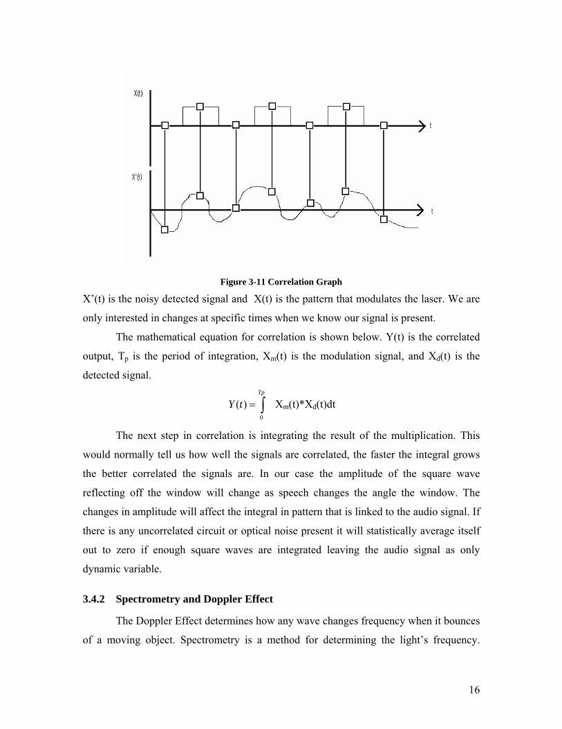
Figure 3-11 Correlation Graph
X’(t) is the noisy detected signal and X(t) is the pattern that modulates the laser. We are
only interested in changes at specific times when we know our signal is present.
The mathematical equation for correlation is shown below. Y(t) is the correlated
output, Tp is the period of integration, Xm(t) is the modulation signal, and Xd(t) is the
detected signal.
∫=Tp
tY0
)( Xm(t)*Xd(t)dt
The next step in correlation is integrating the result of the multiplication. This
would normally tell us how well the signals are correlated, the faster the integral grows
the better correlated the signals are. In our case the amplitude of the square wave
reflecting off the window will change as speech changes the angle the window. The
changes in amplitude will affect the integral in pattern that is linked to the audio signal. If
there is any uncorrelated circuit or optical noise present it will statistically average itself
out to zero if enough square waves are integrated leaving the audio signal as only
dynamic variable.
3.4.2 Spectrometry and Doppler Effect
The Doppler Effect determines how any wave changes frequency when it bounces
of a moving object. Spectrometry is a method for determining the light’s frequency.
17
The Doppler Effect changes light by lowering its frequency when it strikes an
object moving away from it, and increasing its frequency when it strikes an object
moving toward it. Spectrometry works with a prism, when light is passed through a prism
it is bent at an angle depending on its frequency.
The Doppler Effect is relevant to our project because the frequency of our laser
may change depending on if the window is moving forward or backward when the wave
strikes it. A sensitive enough spectrometer could detect minute changes in frequency
caused by the moving window. The changes in frequency could be linked to the audio
signal.
3.4.3 Time of Flight
The time of flight method measures the position of an object by pulsing energy at
it and measuring the time it takes for it to return. In our case the time of flight method
would require very fast and sensitive equipment so that very small and fast movements of
the window cause by speech could be track. If the position of the window were known at
enough moments in time the audio signal could be retrieved by taking the derivative of
the position.
18
4 Methodology This section explains the methodology we used to develop a plan of
implementation. Our project took place in six phases. We first brainstormed to develop a
list of possible techniques we could use to solve our problem. Next we narrowed down
the options using our project constraints and resources available as guidance. Once we
had narrowed down the field to only the most feasible options we picked one and tried to
prove the concept. After proving the concept we proceeded to refine the concept. The
plan was to stop refining the project and begin to finalize it once we had met the projects
goals or when time became an issue. Finalization included testing the prototype’s
specifications and limitations. The last phase in our plan was to offer any
recommendations to anyone wishing to follow up on our work.
4.1 Investigation of Possible Implementation Methods The first phase that we underwent was to come up with as many possible methods
for implementation of our project that we could. None of the ideas were immediately
rejected. A seemingly unfeasible idea may not be able to stand alone but it needs to be
considered because certain parts of it may be applicable to another idea.
The ideas we came up with from brainstorming included interferometry, Walsh
function correlation, time of flight, and Doppler shift. The basic theory behind these ideas
is covered in the background chapter. To narrow down our choices we needed to find out
which ones were the most feasible. We established feasibility by performing simple
calculations. If the method worked in theory we enquired as to the cost of the equipment
to measure the phenomena. If it was outside our budget the idea was disregarded.
4.1.1 Time of Flight
The first idea we examined was time of flight. The idea was to send out a pulse of
laser light then determine the amount of time it took for the light to return. Since the
distance from the laser beam to the window should change with the audio signal, the
audio information could be retrieved.
The idea proved to be impractical. It works in theory, but instruments required to
measure such small vibrations are beyond out resources for this project. Time of flight is
19
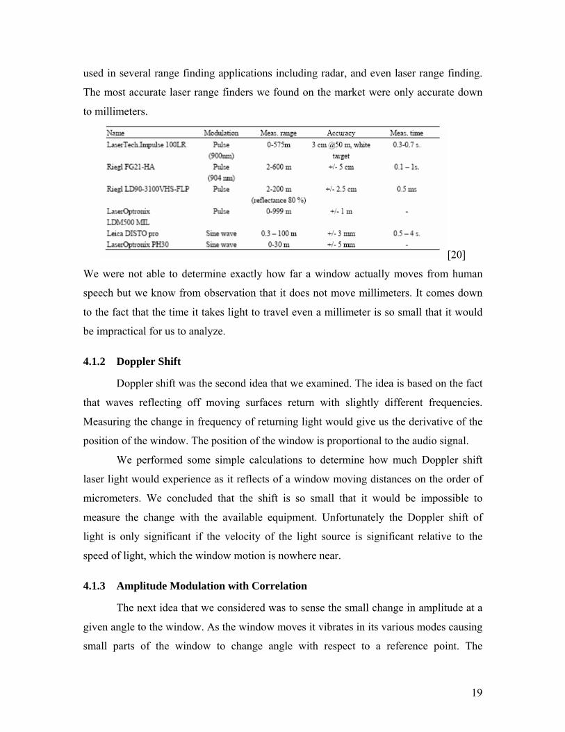
used in several range finding applications including radar, and even laser range finding.
The most accurate laser range finders we found on the market were only accurate down
to millimeters.
[20]
We were not able to determine exactly how far a window actually moves from human
speech but we know from observation that it does not move millimeters. It comes down
to the fact that the time it takes light to travel even a millimeter is so small that it would
be impractical for us to analyze.
4.1.2 Doppler Shift
Doppler shift was the second idea that we examined. The idea is based on the fact
that waves reflecting off moving surfaces return with slightly different frequencies.
Measuring the change in frequency of returning light would give us the derivative of the
position of the window. The position of the window is proportional to the audio signal.
We performed some simple calculations to determine how much Doppler shift
laser light would experience as it reflects of a window moving distances on the order of
micrometers. We concluded that the shift is so small that it would be impossible to
measure the change with the available equipment. Unfortunately the Doppler shift of
light is only significant if the velocity of the light source is significant relative to the
speed of light, which the window motion is nowhere near.
4.1.3 Amplitude Modulation with Correlation
The next idea that we considered was to sense the small change in amplitude at a
given angle to the window. As the window moves it vibrates in its various modes causing
small parts of the window to change angle with respect to a reference point. The
20
amplitude of light gathered at the reference point is proportional to the angle change
which is in turn proportional to the audio signal.
We determined that this method was feasible if we devised a way to detect very
small changes in very small signals. A technique called Walsh function correlation was
recommend by our advisor. We investigated the feasibility of the idea and found that it
was within our means to create a system based on correlation. This technique is capable
of retrieving extremely small signals that are even smaller than noise floor. The theory of
this concept was discussed in the background section.
4.1.4 Interferometry
The final idea that we examined was interferometry. Interferometry measures
interference pattered in beam of light that is split then recombined. It can be used as a
very sensitive method of determining distance if one light path is of a known distance and
the other is not. The fringe pattern created when the beams are recombined can be used to
determine the unknown distance with accuracy on the order of nanometers – the
wavelength of a laser. After considering our resources which included access to high
precision optical equipment we determined that the interferometry approach was
possible.
4.1.5 Proof of Concept
About 1/3 through the first term of our project we had narrowed the possible
methods to down to interferometry and correlation. Ideally the next step was to
experiment with each concept and decide which was better aligned with our project goals.
The constraints of time and manpower however made this unfeasible. We decided to try
correlation first; if it worked then we would refine the concept. If we could not prove the
correlation concept we would fall back on interferometry.
We worked on the correlation concept, first by concretely proving the concept
that light amplitude was proportional to angle change. This was done by mounting
window on a vertical axis of rotation and measure light at our detector at different
window angles. The experiment included a variation on an opaque surface, and a
scratched section of a window. The full results of this experiment were shown in the
background section. As discussed, the experiment showed that the angular distribution of
21
light was not uniform, and therefore a small change in angle of the window would result
in an amplitude change.
This led us to the conclusion that if we could detect small enough levels of light
accuracy, we should be able to use this amplitude modulation to retrieve our audio signal.
This was the detection method that we decided to pursue.
4.2 Refinement of Design Our correlation concept proven, we moved on to the refinement of concept phase
of our project. Our plan for refinement was to replace all of our control functions with a
digital signal processor then step though the circuit from the optics module to the audio
driver replacing low frequency components with components better suited for high
frequency applications.
After determining our detection method, we developed an idea of all the modules
that would eventually constitute our project. The first module would drive the laser diode.
Next, the optics would gather the faint traces of light gathered from the distant window.
The light would be detected by the detector module and sent through a gain module. The
signal would then be processed by correlating it with the Walsh function used to drive the
laser. A digital signal processor could then be used to sample the signal, process it, and
then output it through a digital to analog converter. Once the signal was cleaned up by the
processor it would be sent to an audio driver stage and output to headphones.
4.2.1 Laser Diode Driver
As we chose a laser as the light source for our project, we needed to have some
means to drive it. We looked into the possibility of using pre-made laser modules that
drove the laser and collimated the laser beam. Although using such a module would have
saved us a considerable amount of time, the prices of these systems were beyond our
budget range. Ultimately we decided to implement our own laser diode driver circuit to
power a laser diode of our choosing. We understood that laser diode driver circuits could
be quite complicated, but strove to design one that was as simple as possible to fulfill our
needs.
We also determined that we would need to modulate our laser beam with a square
wave for two reasons. The first is that the correlation principle that we were trying to
22
exploit requires it. Also, but modulating the laser beam, the audio information we were
interested in would be moved up in the frequency band, much higher than any other light
source, so we could easily filter out the undesired light that we detected with a high pass
filter.
4.2.2 Optics
The optical system we decided to implement consisted of a laser diode,
several lenses and a window. We shone the laser beam through lenses to collimate the
beam; then had that beam incident on the window. The light reflected back from the
window then needed to be concentrated on to our photodiode, as we sought to create an
optics module that delivered as much light to the detector as possible.
We considered two major ideas for light collection, which were the parabolic
reflector and a Fresnel lens. The parabolic reflector acts as a satellite dish for light.
Parallel rays of light traveling from a point in front of the detector enter and reflect off
the surface of a parabola and are all focused to the detector. The cost of obtaining a
quality reflector and the fact that a large reflective dish is not very covert were the factors
that led to the idea being disregarded.
The Fresnel lens proved to be the superior idea. In theory it provides the same
amount of light for its area, and we simply knew more about how well Fresnel lenses
worked. We did not have the luxury of research time so we went with what we knew.
It is also important to note that we chose to use a laser in the visible spectrum.
Ideally a device meant for covert use such as this would not use visible light since it
could be seen by the party that is being eavesdropped upon. An infrared laser would be
used for a final implementation of this device. We chose to use a visible laser however
for ease of use in the laboratory experimentation we were conducting, as it would be
more difficult to keep track of the location of an infrared laser beam.
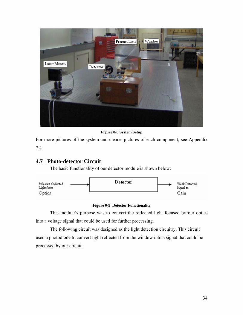
4.2.3 Detection
We understood that we had a challenging problem in that we were trying to detect
very small levels of light, the backscatter reflected from a window. Furthermore however,
we also were trying to detect light at our modulation frequency which needed to be
23
relatively high. In detecting light, there is always a tradeoff of sensitivity versus
responsivity, which we needed to adapt to our needs.
The first stage of our circuit needed to have a light detector. We were able to
easily determine that our detector needed to be a photodiode, as they are the only type of
detector with the time response we required. Both phototransistors and photocells are too
slow. Photodiodes come in different types. The “active area” of a photodiode is the area
of the photodiode that is sensitive to light. The larger this area is, the more light will be
detected. The tradeoff is that this active area is part of an internal capacitance in the
diode, so the larger the area the more capacitance is present. The larger this capacitance is
the worse the response time of the diode. We chose a photodiode which we felt would be
suitable to our needs, although it was not possible to know precisely what the best active
area size was for our needs.
A photodiode acts like a current source when it is in reverse bias, putting out a
small current linearly proportional to the amount of light incident on the active area. This
current is very small, generally on the order of micro-amps. Considering we were trying
to detect very small levels of light, we knew that we would need to carefully design
circuitry to retrieve a signal from this small current in order to convert it back into audio.
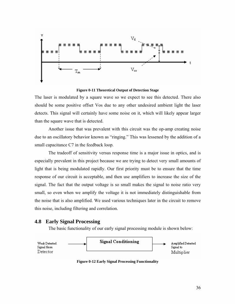
4.2.4 Early Signal Processing
The problem of trying to extract information from a very small signal was the
major issue in this project. We expected the size of the signal we obtained from the
photodiode to be so small that it was smaller then the noise that was also in the circuit.
For this reason we needed to use the correlation technique described in the background
section.
Before we could do this however, we needed to perform some initial signal
processing. We needed to remove any undesired light signal that was not from the laser.
We decided the best way to do this was to modulate the laser beam with a high frequency
wave. The laser should be the only light source detected at a high frequency, so a high
pass filter should rid the signal of any undesired light information. Since our signal was
so small we would almost certainly need to provide additional gain. We also anticipated
24
that other methods of early signal processing may present themselves to enhance the
performance of the system even further.
4.2.5 Correlation
In order to extract a signal so small that it is likely smaller than the noise in the
circuit, we needed to use the correlation technique described in the background section.
This technique is described mathematically as the integral of two signals multiplied, the
measured signal and a reference signal. We needed to achieve this mathematical
operation in circuitry. First, we needed to be able to multiply the two signals. We already
planned on modulating our laser beam with a high frequency wave for reasons previously
stated. We decided to make this wave a square wave to make the correlation process
simpler. Binary multiplication is relatively convenient in circuitry. Since it entails either
multiplying by one or zero, that means simply to either let the detected signal through or
let a zero through. This can be achieved fairly simply in circuitry with as little as one
transistor.
We also had to perform the operation of integration. The most common manner in
which to integrate a signal is using an op-amp integrator. At the beginning of each new
integration period this integrator would need to be reset to begin the operation again. The
more cycles of the modulation frequency are contained in one integration period the more
robust the output will be, diminishing the noise content. At the end of each integration
period, the value of the integral will ideally be linearly proportional to the amplitude of
the detected signal, and therefore effectively a sample of the audio signal that we wish to
reconstruct. This sample will then go into to digital domain for further processing.
Since we were trying to represent human speech with these samples, ideally we
should have twice as many samples as the highest frequency we with to capture. Human
speech is mostly contained between 20 and 2000Hz, though it can go as high as 3600Hz.
We decided to implement the system with a 4000Hz sampling frequency however, at
least for initial testing. The correlation technique works such that the more pulses that are
integrated per reset period the SNR is increased linearly. For this reason we strove for a
modulation frequency of 4MHz, so we would have 1000 pulses per integration period,
and hopefully a good SNR for further processing.
25
4.2.6 Digital Signal Processing
The purpose of the digital processing module is to provide control signals to the
rest of the circuit, and to extract the audio signal from the correlated signal. When we
first conceived the idea of using a DSP to replace several analog circuits we were not
very knowledgeable about the DSPs on the market. Through some preliminary research
consisting asking people who use DSPs what they thought, we came up with 2 major
families of DSPs.
The two families were Texas Instruments DSPs and Microchips dsPICs. We had
to make a decision quickly due to time so the criteria we used to choose a DSP was not
extensive. The criteria we used to choose between our options were cost, ease of use,
resources available at WPI, and the processors abilities.
Cost was an issue because we had a limited budget and DSPs with a lot of
peripherals can get expensive. Ease of use was an important aspect of the DSP because
we only had one term left to get it up and running. We included processor abilities we
had a general idea of what features we were looking for including a fast clock speed, and
analog to digital converter, and a digital to analog converter.
We investigated cost by researching on the internet as well as asking
knowledgeable people. We came to the conclusion that most dsPICs cost under $20. [21]
The only information we had on TI DSPs was that the development boards cost $395.
After looking at the TI website it became clear that most of their products came in
expensive packages and we opted to not sift through the website when we knew dsPICs
were within our price range and available at Digi-Key.
As far as ease of use the dsPIC was the clear winner. The dsPICs can come in 28
or 40 pin DIP packages that can fit into proto-boards. The TI DSPs that we looked at all
came in 44 pin surface mount. Another factor that we considered is that we both had
experience with PIC microprocessors and we both had none with the TI chips.
The analysis of resources available at WPI to program and debug also favored the
dsPIC. There was an in circuit debugger and programmer available from the ECE shop.
The only TI chips we that we had seen programmed at WPI were attached to expensive
development boards.
26
If the DSP could not replace much of the analog circuitry then it was not much
use to us. To determine which family of DSPs had the abilities we required we started
determining the I/O functions we wanted it to perform. Also at this point we knew that if
the dsPIC could do what we wanted to be done we were going to choose it regardless of
what the TI chip could do.
The DSP needed to take in an analog signal, convert it to digital, perform some
processing and then output an analog signal. So we knew that we needed a DSP that had
an A/D converter as well as a D/A converter. We also wanted it to generate a high
frequency square wave to modulate the laser diode. This was not a problem for many of
the dsPICs we looked at which had clock frequencies over 100Mhz without an external
oscillator. We also wanted the DSP to reset the integral. This signal could just be a pulse
from one of the I/O pins, well within the dsPICs ability.
Our final choice came down to battle between different dsPICs. We initially
ordered a dsPIC 30F4013 because we overlooked the fact that it did not have a D/A
converter. In fact none of the dsPICs had one built in.
At this point we face a dilemma as to whether to buy a digital to analog converter
or build our own. We checked around with people familiar with DSP and found that it
could be troublesome to get different ICs to connect to each other properly. We also were
told that we could make a pulse width modulated PWM output and use a low pass filter
to convert a digital signal to analog.
We decided to pursue the PWM path. Through online research we found that the
dsPIC30F4011 had a PWM output pin built in, and subsequently ordered one. Within a
week we had the AD converter and PWM output functioning together. Unfortunately we
destroyed the AD converter when we tried to hook it up to the rest of the circuit.
The failure of the dsPIC30F4011 gave us two options, order another and wait a
week, or build a PWM program from scratch on the dsPIC30F4013. Due to the time
consideration we decided on generating our own PWM code because we thought it would
take less then a week to create it. Hence the dsPIC30F4013 became our DSP.
27
4.2.7 Audio Driver
Our audio driver module was never integrated into the system because we ran out
of time. The purpose of the audio driver was to amplify the DSPs filtered output signal to
drive a speaker. The most important criterion for the audio driver module was ease it’s of
design. The module was not a critical part of our project and we did not want to spend
much time on it. We decided on using the same IC as last years project, and got as far as
implementing it on its own before more pressing needs in the circuit drew out attention
elsewhere.
4.2.8 System Integration
We integrated our system module by module starting at the front end of circuit
and working our way through to the end. We found that there is great importance in a
well planned methodology for system integration.
During the integration of our system we would isolate a module and test it for
functionality, then do the same with the next module. When both modules functioned
worked we would combine them and check for functionality. After achieving
functionality more modules were added until we reached the end of the circuit. Our
system that we developed allowed us to better isolate problems, the times when we failed
to follow the system we wasted hours trying to track down problems.
4.3 Summary The methodology we used to complete our project had us starting off with a
broad array of concepts and ideas that we narrowed down to a couple of concepts we
thought were provable. We attempted to prove the one that was more inline with our
project goals and succeeded.
From that point on we endeavored to refine the concept until we met our project
goals or until time became and issue. We worked through each module and determined
the general method for implementing each one. Then we worked to implement each of
the modules before finally linking them up to form a final system.
When the time constraint put a halt to our design work we performed final testing
to see if we meet specs and find the limitations of our system. The final phase of our
project was to offer any recommendations on how to further refine the system.
28
Implementation This chapter is a record of the implementation of the plan we developed in the
methodology section. We will present all of the details of the system we designed to
accomplish our objective. We will first present an overview of how the various modules
in our system function together. Then we will get into the specifics of each of the
modules. Within each module’s section we will review its role in the system, list the
options if any we had for its implementation, and explain how it was finally implemented
including any problems we had along the way.
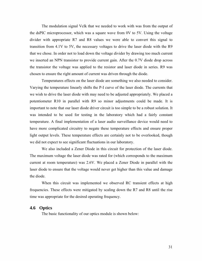
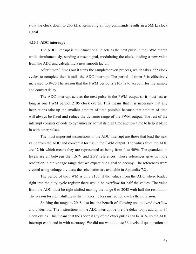
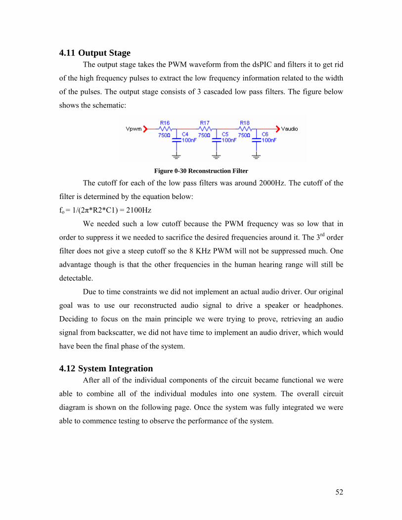
4.4 General Functionality The following figure is our system block diagram which shows the overall
depiction of our system and how the various subsystems interconnect.
Figure 0-1 System Block Diagram
29
Our system collimates and modulated laser beam and projects it against a
window, uses optics to focus that beam onto a receiver circuit, does some early signal
processing, then correlates the signal to remove noise, digital signal processing, and
reconstructs the analog audio signal before we drive a head phone speaker with the audio
signal begin generated behind the glass.
We broke this complicated task into several modules to simplify the design
process. The driver circuit will modulate a laser diode at the required frequency. Optics
will be used to collimate light from the laser diode and receive light being reflected off
the window. A very sensitive and noise free detector circuit is needed to sense the weak
modulated light delivered by the optics. A gain stage is required to boost the signal up to
more manageable amplitude. Then the process of correlation can begin, first by using a
multiplier stage to find the product of the modulation signal and the detected one. Then
we will use an integrator circuit to add up the area under the product signal, which is
proportional to the audio signal.
The signal next moves into the digital domain. The digital portion of this project
performs real time digital signal processing as well as provides several control signals
used by the rest of the circuit. The DSP samples the correlated signal, quantizes the result
then resets the integrator at the sampling frequency. The signal is then output via pulse
width modulation. The DSP also provides the modulation signal for the laser diode and
multiplier circuit as well as the inverse of the modulation signal also used by the
multiplier. The output of the DSP is pulse width modulated and needs a reconstruction
stage which consists of an analog low pass filter to return it to an analog signal. Then the
signal can finally be used to drive an audio amplifier IC designed to power headphones.
4.5 Laser Diode Driver The basic functionality of our laser diode driver module is shown below:
Figure 0-2 Laser Diode Driver Functionality
30
The purpose of this module was to drive our laser diode, modulating it with a pulsed
waveform generated by the dsPIC.
The following circuit was designed in order to drive the laser diode that was
selected.
Figure 0-3 Laser Diode Driver Circuit
We needed to drive our laser diode with a modulated current so that it would pulsate at
the modulation frequency. As mentioned in the background section, when modulating a
laser beam it is important to not turn the laser completely off, because it takes a certain
amount of time to turn back on which is significant at high frequencies. Because of this,
lasers that are pulsed are generally pulsed between a bright state and a dim state.
We selected a 7mW laser with a wavelength of 650nm, which is red light. We
chose to work with a visible frequency of light for convenience of prototyping in the
laboratory. For a final implementation of a laser audio surveillance device an infrared
laser should be used so that it is not immediately obvious that a laser is incident on the
window.
We desired our laser diode to be switched between two states, bright and dim. The
bright state corresponded to approximately 45mA of current through the laser diode,
while the dim state needed to be about 30mA to ensure that it was always above the
threshold current of our laser diode. By placing a resistor R9 in series with the laser
diode, and applying a voltage to it, we could drive a certain current through the laser
diode. By changing this voltage with time, we could modulate the laser diode with
different amounts of current.
31
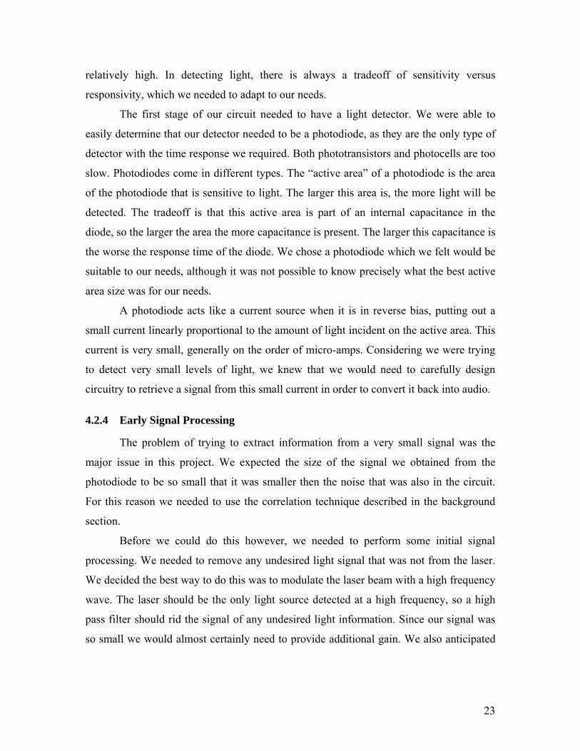
The modulation signal Vclk that we needed to work with was from the output of
the dsPIC microprocessor, which was a square wave from 0V to 5V. Using the voltage
divider with appropriate R7 and R8 values we were able to convert this signal to
transition from 4.1V to 5V, the necessary voltages to drive the laser diode with the R9
that we chose. In order not to load down the voltage divider by drawing too much current
we inserted an NPN transistor to provide current gain. After the 0.7V diode drop across
the transistor the voltage was applied to the resistor and laser diode in series. R9 was
chosen to ensure the right amount of current was driven through the diode.
Temperatures effects on the laser diode are something we also needed to consider.
Varying the temperature linearly shifts the P-I curve of the laser diode. The currents that
we wish to drive the laser diode with may need to be adjusted appropriately. We placed a
potentiometer R10 in parallel with R9 so minor adjustments could be made. It is
important to note that our laser diode driver circuit is too simple to be a robust solution. It
was intended to be used for testing in the laboratory which had a fairly constant
temperature. A final implementation of a laser audio surveillance device would need to
have more complicated circuitry to negate these temperature effects and ensure proper
light output levels. These temperature effects are certainly not to be overlooked, though
we did not expect to see significant fluctuations in our laboratory.
We also included a Zener Diode in this circuit for protection of the laser diode.
The maximum voltage the laser diode was rated for (which corresponds to the maximum
current at room temperature) was 2.6V. We placed a Zener Diode in parallel with the
laser diode to ensure that the voltage would never get higher than this value and damage
the diode.
When this circuit was implemented we observed RC transient effects at high
frequencies. These effects were mitigated by scaling down the R7 and R8 until the rise
time was appropriate for the desired operating frequency.
4.6 Optics The basic functionality of our optics module is shown below:
32
Figure 0-4 Optics Functionality
The purpose of this module is to take the modulated laser beam and reflect it off of the
surface of a vibrating window, then collect the reflected light onto a photo-detector.
Before we could have our laser beam shine on a window surface we needed to
shape the light from our laser diode into a tight collimated beam. The light coming out of
our laser diode had a divergence angle of about 30 degrees. In order to change this into a
collimated beam we needed to use a lens system.
Figure 0-5 Collimation Optics
The light from the laser diode was first sent through a convex lens to take the
diverging light and focus it back in on itself. When the beam reached the desired diameter
(about 3mm) it was collimated using a concave lens. This lens had to be a specific
distance away from the convex lens to achieve collimation, so it needed to be carefully
adjusted.
The laser beam could then be directed onto the window. We used a window
mounted on a rotating platform so we could test the system’s performance when the laser
beam was incident on the window at various angles without having to adjust the laser or
any other optical components.
33
Figure 0-6 Laser and Window Configuration (Side View)
Our detector assembly was arranged with the laser, such that the detector would
always be aimed at the same spot on the window as the laser, the backscatter dot.
Figure 0-7 Laser and Detector Setup (Top View)
We used a large Fresnel lens in order to collect as much light as possible and focus it on
the detector to give us the best signal strength possible. We found when we assembled
these lenses that the Fresnel lens did not focus the light as tightly as we had hoped due to
aberrations. We experimented with using an additional convex lens to try to decrease the
radius of the spot. We had little success with this, as the aberrations had disrupted the
integrity of the light. The improvement was small to negligible.
The picture below shows the setup of our system, indicating the locations of the
key components.
34
Figure 0-8 System Setup
For more pictures of the system and clearer pictures of each component, see Appendix
7.4.
4.7 Photo-detector Circuit The basic functionality of our detector module is shown below:
Figure 0-9 Detector Functionality
This module’s purpose was to convert the reflected light focused by our optics
into a voltage signal that could be used for further processing.
The following circuit was designed as the light detection circuitry. This circuit
used a photodiode to convert light reflected from the window into a signal that could be
processed by our circuit.
35
Figure 0-10 Photo-Detector Circuit
A photodiode in reverse bias will create a current proportional to the light incident on it,
known as the photocurrent. Our photodiode was in reverse bias because its anode was at -
9V and its cathode was at the virtual ground node of an operational amplifier. The
photodiode we chose had a responsivity of approximately 0.5 Amps per Watt of optical
power incident on the detector's active area for the wavelength of our laser, 650nm.
The op-amp configuration we chose to use is called the transimpedence amplifier,
which is used to convert current signals, like what the photodiode creates, and convert it
to a voltage signal.
This photocurrent is forced through R1, because ideally the negative terminal of
the op-amp has infinite impedance. This creates a voltage Vout which is proportional to
the photocurrent. The larger the value chosen for R1, the greater Vout will be via Ohm’s
Law. There are limitations to how large R1 can be however. First, the larger the
resistance chosen for R1 the more thermal noise is introduced to the system. This is
certainly undesirable as the signal should have as little noise as possible. Also, the
resistance R1 in conjunction with any stray capacitance in the circuit creates an RC
transient time response in Vout. Since the stray capacitance is generally fixed, the only
way to improve the time response of Vout is to reduce R4, which reduced the amplitude
of Vout.
The output of this stage should appear like the figure below.
36
Figure 0-11 Theoretical Output of Detection Stage
The laser is modulated by a square wave so we expect to see this detected. There also
should be some positive offset Vos due to any other undesired ambient light the laser
detects. This signal will certainly have some noise on it, which will likely appear larger
than the square wave that is detected.
Another issue that was prevalent with this circuit was the op-amp creating noise
due to an oscillatory behavior known as “ringing.” This was lessened by the addition of a
small capacitance C7 in the feedback loop.
The tradeoff of sensitivity versus response time is a major issue in optics, and is
especially prevalent in this project because we are trying to detect very small amounts of
light that is being modulated rapidly. Our first priority must be to ensure that the time
response of our circuit is acceptable, and then use amplifiers to increase the size of the
signal. The fact that the output voltage is so small makes the signal to noise ratio very
small, so even when we amplify the voltage it is not immediately distinguishable from
the noise that is also amplified. We used various techniques later in the circuit to remove
this noise, including filtering and correlation.
4.8 Early Signal Processing The basic functionality of our early signal processing module is shown below:
Figure 0-12 Early Signal Processing Functionality
37
This module’s purpose was to take the small detected signal from the detection stage and
perform operations on it so that it became ready for the correlation part of the system.
The first objective that this part of the circuit performed was to rid the signal of
any undesired light that would be at lower frequencies such as sunlight (DC) or electronic
lights (generally 60 or 120Hz). Since our laser light was to be modulated much faster
than this, we could use a high pass filter to let only the laser light through. This circuit
was implemented as follows;
Figure 0-13 High Pass Filter Circuit
The cutoff frequency for this filter:
fo = 1/(2π*R2*C1) = 16kHz
This cutoff frequency is acceptable as it is well above the frequencies to be blocked and
well below the modulation frequencies we considered testing with. The output of this
circuit should then look as follows:
Figure 0-14 Theoretical High Pass Filter Output
Any DC offset or low frequency disturbance should now be removed from the signal,
leaving the desired signal averaged about ground.
Next we needed to provide the signal with additional gain in order create a large
signal much larger than the noise in the circuit, so that the signal would not be further
deteriorated by noise in further stages. Any noise the signal already had on it however
would be amplified along with the signal. This gain stage was implemented as follows:
38
Figure 0-15 Gain Stage
The circuit used was a standard non-inverting amplifier with a gain of about ten to
amplify the signal. The output of this circuit should appear as follows:
Figure 0-16 Theoretical Output of Gain Stage
The signal should be identical to the input signal, including any noise, but multiplied by
the gain factor.
Next we decided to implement a clamping circuit, to take the output of the gain
stage and clamp the bottom of the signal to ground. This would prove useful later when
we needed to integrate the signal later, providing twice the area to be integrated for a
stronger signal. This circuit was implemented as follows:
39
Figure 0-17 Clamper Circuit
The output of this circuit should be the same as the output of the gain stage, but with the
bottom of the signal clamped to ground. Normally a clamper circuit of this nature would
clamp its output to -0.7V due to the voltage drop across the diode. For this reason we set
our clamper to a 0.7V reference voltage to ensure the clamping was really to 0V. To view
the implementation of this voltage reference, see Appendix 7.2. The output of this circuit
should look as shown below.
Figure 0-18 Theoretical Output of the Clamper Circuit
After all of these stages of signal processing, our signal was finally ready to undergo the
process of correlation to rid it of the noise that overwhelmed it.
4.9 Correlation
The basic functionality of our correlation consists of two parts, multiplication and
integration. The functionality of the multiplier is shown below.
40
Figure 0-19 Multiplier Functionality
This module was realized as a circuit as follows:
Figure 0-20 Analog Multiplier
This circuit either lets the input signal pass through to the output or sends ground to the
output based on the inverted modulation signal which comes from the dsPIC. When Vclk
is high, the laser out put is high and we desire to let Vin pass through to the output. Vclk’
is therefore low which makes the NMOS transistor in this circuit act like an open circuit
between Vout and ground. Vout is a high impedance node, so there is practically no
current through R5 and therefore no voltage drop across it, so Vin = Vout. When Vclk is
low however, we desire Vout to be 0V. Vlclk’ is high and the NMOS transistor acts like a
short circuit between Vout and ground, forcing Vout to equal 0V.
The output waveform would then ideally behave as depicted below:
Figure 0-21 Theoretical Output of Multiplier
41
The result of which is the desired multiplication of the detected signal by the clock signal
that modulates the laser beam.
Next this signal needed to be integrated to complete the process of correlation.
The functionality of this module is as follows:
Figure 0-22 Integrator Functionality
This module was realized as circuitry as follows:
Figure 0-23 Integrator with Reset Switch
The main component of this module is a standard op amp integrator. The output of the
op-amp in this configuration is as follows:
Vout = -1/(R6*C3)*∫ Vin(t)dt
So, the output of the integrator will be the inverted integral of the input, scaled by the
chosen R6 and C3. We chose the values of R6 and C3 so the integrator would integrate at
the desired rate.
Since the input of this circuit is the output of the multiplier, which is always
positive, we would expect to see this integrator output decrease as it integrates until it hits
the negative rail. This would not be very useful, which is why it is necessary to reset the
42
output of the integral periodically to some known value. In our case we chose 5V. The
destination of the output of this circuit is the dsPIC’s analog to digital converter, which
needs an input voltage between0V and 5V. By resetting the integrator output to 5V and
knowing it always integrates downwards, we can assure this happens. The output of the
integrator should appear as follows:
Figure 0-24 Theoretical Output of Integrator
The peaks of this waveform should correspond to the amplitude of the desired audio
signal.
The reset action is performed by a PMOS switch, with an input signal Vreset from
the dsPIC. When the integrator is integrating Vreset is high, making the PMOS act like
an open circuit between the output of the op-amp and 5V. When the integrator needs to
be reset, Vreset goes low and causes the PMOS to act like a short circuit between the
output of the op-amp and 5V, resetting the output to 5V for the next integration period.
Since the op-amp was being supplied by +/-9V rails, it was possible that the
output voltage could go below ground, which is outside the range that the dsPIC can
interpret, and possibly even damaging to the dsPIC. For this reason we placed a 5.1V
Zener diode at the output of the op-amp. This Zener diode ensures that the voltage stays
between 0V and 5V.
We also ran into an issue where the dsPIC’s analog to digital converter drew more
current than the LM741 op-amp we were using could provide. We then decided to use an
NPN transistor to provided current gain so this was no longer an issue. This transistor
does introduce a 0.7V drop, however this small shift in the voltage range proved to be
inconsequential as long as Vout did not get too low, which was easy to control.
43
4.10 Digital Signal Processing The dsPIC30F4013 samples and converts the analog signal Vint, processes it,
then outputs a pulse width modulated version of the signal. The dsPIC also provides
control signals to laser diode driver, multiplier, and integrator. This section will present
the exact setup we used to develop and implement dsPIC programs, and an in depth
explanation of functionality of the final program.
The main functionality of this module is shown below:
Figure 0-25 Digital Signal Processing Functionality
4.10.1 Setup
Using the dsPIC required several resources that are in the standard lab kit or
available either at WPI or as shareware online. The resources include a development
environment, a programmer/debugger, and special hardware to allow programming of the
dsPIC while it’s on a breadboard.
Our development environment was MPLAB IDE v7.22 with the Microchip C30
language tool suite which includes a C compiler. Using MPLAB we compiled our C code
and simulated it with software debugger MPLAB SIM. The latest version of MPLAB
IDE is available on the Microchip website free of charge. The C30 C complier is
available as a 60 day free trail online.
The programmer/debugger we used was Microchips In Circuit Debugger (ICD) 2
which was meant to be used with MPLAB. In debugger mode the ICD 2 programs special
instructions into the dsPIC which allowed us to step though the loaded program and set
breakpoints. In programmer mode the ICD 2 loads the program and is disconnected
allowing the dsPIC to run itself.
44
We did not have a development board to work from so we needed to find a way to
program the dsPIC directly from the ICD 2. We looked up the pin out of the dsPIC on the
spec sheet and found which pins were used for programming. We then cut the cord from
the ICD 2 into its individual wires and ran them to the appropriate pins on the dsPIC.
[22] Figure 0-26 dsPIC Pinout
The wires from the ICD are numbered 1 through 6 and are connected to MCLR, Vdd,
ground, PGD, PGC, and nothing, respectively. MCLR is pin 1 in the figure above, PGC,
and PGD are 8 and 9 respectively. MCLR should also be connected to power with a 1k
ohm resistor.
The circuit diagram for this part of the system is shown below:
Figure 0-27 dsPIC Circuit Diagram
In our final system we used pins for power and ground, the PWM output, ADC
input, the clock outputs, and the integral reset signal. In the picture above all pins marked
Vdd and Vss were power and ground respectively. The PWM output was pin 16
PORTC14. The ADC input was pin 4 AN2. The voltage references for the ADC were pin
45
2 and 3, Vref+ and Vref- respectively. The clock outputs came from pins 28 and 29
PORTF1 and 4 respectively. The integral reset signal came from pin 22 or PORTD2.
4.10.2 The Program
The final program for the dsPIC performed all the signal processing and generated
all control signals required without external digital components or oscillators. The dsPIC
does not have multiple functional units so we did not have the benefit of running
instructions in parallel either. The code multitasked by using timers, interrupts and calling
assembly language functions. This section will first give a general overview of the code
and then get into the details of each function and interrupt.
The program consists of a main function, square wave function, configuration
function, an ADC interrupt triggered by a Timer 3 countdown, a PWM frequency
triggered by timer 1 interrupt, and a PWM duty cycle interrupt triggered by timer 2.
The flowchart for the code is illustrated in Figure 0-28. The main program
initializes I/O ports and calls the configuration function. Then main calls the square wave
function that infinitely loops until the ADC interrupt is called. The ADC interrupt
continues to generate a slower version of the square wave as it updates the duty cycle
data for the next four pulses, gives the reset signal to the integral, and finally returns to
the square wave. The PWM frequency interrupt is immediately called thereafter. The
PWM frequency interrupt sets the PWM pin high then returns to square wave. After the
appropriate amount of time the duty cycle interrupt is called and the PWM pin is set low.
The output remains low until the frequency interrupt is called again. This cycle repeats
for 3 pulses then the ADC interrupt is called for an update.
46
Figure 0-28 Program Functionality
4.10.3 Configuration
The purpose of the configuration function is to initialize the analog to digital
converter, and timers 1, 2 and 3 to correctly implement the flowchart in the above figure.
The dsPIC is designed to perform many diverse tasks; setting the right bits in
configuration registers allowed us to specify its exact behavior.
The purpose of the ADC was to get one sample of the integral at its peak and
convert it to a 12 bit digital number. We used AN2 as the input for the analog signal, we
had to specify that it was analog pin and that it was and input pin. There are many pins on
the ADC so we had to specify the AN2 was the one to be read by the sample and hold
amp inside the dsPIC.
There were many options on how to trigger a sampling and converting of the
analog input. We had to specify that a timer 3 time out triggers a sample convert
progression. We had to specify that only one sample be taken per such progression and
that it is represented as an unsigned integer. When the ADC was finally configured the
correct way it was turned on.
Each of the timers needed to be set as 16 bit counters that count up to the value in
a period register then reset to zero and call and interrupt. Timer 3’s period is fixed and it
47
determines the sampling rate of the analog signal. Timer 1’s period is fixed and it
determines the frequency of PWM. Timer 2’s period is initialized to 0, it determines the
PWM duty cycle by changing based on the values sampled by the ADC.
Our final project ran off the dsPIC’s 120MHz internal clock. One timer clock
cycle is equal to 4 system clock cycles. We wanted to sample and reset the integral at 4
KHz. We used equation X to find the correct answer.
40004/000,000,12075004/3 =→=
FskSystemClocPR
The correct answer is 7500 but for reasons explain later on we made it the closest power
of 2, 8192.
Timer 1’s period determined the frequency of pulse width modulation. It was
desirable to keep the frequency out of the range of human hearing but for reasons
explained latter we decided four pulses per sampling was a good idea chose 2105 as
Timer 1’s period.
The final stage in the configuration process is to enable the ADC, timer 1, 2, and
3 interrupts after clearing their respective flags to avoid an instance vector to them.
4.10.4 Main
The purpose of the main function is to tie everything together. It calls the
configuration function as well as configuring the reset of I/O pins used by the rest of the
program. PORTC is used for the PWM output, PORTD is used for the integrator reset
signal, and PORTF is used for the inverted clock signals, they must all be set to digital
output pins. PORT F is loaded with a special value that ensures the negation operator
will provide inverted clock signals. The remainder of main is and infinite loop that calls
the square wave function.
4.10.5 Square Wave
The square wave function creates the clock signal that modulates the laser diode
driver, and multiplier. The function is in assembly because only assembly is fast is fast
enough to meet our original goal of our system which was 4 MHz clocks. Our project
was never able to achieve 4MHz operation so we had to put several nop commands to
48
slow the clock down to 200 kHz. Removing all nop commands results in a 5MHz clock
signal.
4.10.6 ADC interrupt
The ADC interrupt is multifunctional, it acts as the next pulse in the PWM output
while simultaneously, sending a reset signal, modulating the clock, loading a new value
from the ADC and calculating a new smooth factor.
After timer 3 times out it starts the sample/convert process, which takes 222 clock
cycles to complete then it calls the ADC interrupt. The period of timer 3 is effectively
increased to 8420.The reason that the PWM period is 2105 is to account for the sample
and convert delay.
The ADC interrupt acts as the next pulse in the PWM output so it must last as
long as one PWM period, 2105 clock cycles. This means that it is necessary that any
instructions take up the smallest amount of time possible because that amount of time
will always be fixed and reduce the dynamic range of the PWM output. The rest of the
interrupt consists of code to dynamically adjust its high time and low time to help it blend
in with other pulses.
The most important instructions in the ADC interrupt are those that load the next
value from the ADC and convert it for use in the PWM output. The values from the ADC
are 12 bit which means they are represented as being from 0 to 4096. The quantization
levels are all between the 1.67V and 2.5V references. These references give us more
resolution in the voltage range that we expect our signal to occupy. The references were
created using voltage dividers; the schematics are available in Appendix 7.2 .
The period of the PWM is only 2105, if the values from the ADC where loaded
right into the duty cycle register there would be overflow for half the values. The value
from the ADC must be right shifted making the range 0 to 2048 with half the resolution.
The reason for right shifting is that it takes up less instruction cycles then division.
Shifting the range to 2048 also has the benefit of allowing use to avoid overflow
and underflow. The instructions in the ADC interrupt before the delay loops add up to 36
clock cycles. This means that the shortest any of the other pulses can be is 36 so the ADC
interrupt can blend in with accuracy. We did not want to lose 36 levels of quantization so
49
we coded that pulse lengths always be 36 longer than they really were. So now the
shortest a pulse could be was 36 and the longest was 2084, still below the 2105 limit.
The next step was to store the past duty cycle period into the “past” variable then
move the new value between 0 and 2048 into then “present” variable. We use these two
values and the number of pulses between updates to calculate a smooth factor that is
added to the duty cycle after each pulse. This means that the most recently read value will
not actually be the length of the pulse until the next interrupt is called. The pulses in-
between will slowly approach the new value from the old value.
The rest of the interrupt consists of the delay loops that try to make the interrupt
blend in with the other pulses. There are two delay loops; the first one is followed by an
instruction to end the duty cycle, the next loop keeps the duty cycle low for the remainder
of the interrupt.
The interrupt always lasts 2105 clock cycles. We calculated that it would take
around 275 iterations through a “for loop” to reach 2105 clock cycles every time. The
goal was have to high time equal the amount of high time prescribed by the previous
value read by the ADC. We had to make the ratio of high time to low time translate from
a 2048 point scale to a 275 scale. Instead of using 275 we converted it down to 256 so
that values would map more accurately from a 2048 scale. The 256 iterations of the delay
loops caused the interrupt to last almost 2105 instruction cycles so several meaningless
delay lines were added at the end of the interrupt.
Through experimentation we found that 256 iterations divided between 2 “for
loops” was the same as all 256 iteration given to one loop. The value of the index in the
“for loop” is derived from the previous value that was sampled. The past value was right
shifted 4 times to bring it down to the 256 point scale. The index for the second loop was
defined as 256 minus the first delay number; this was done to maintain a constant
duration for the interrupt. Rather than waste the time during the delays the “for loops”
negate PORTF which continues to modulate the systems clock and inverted clock.
The other responsibility of the ADC interrupt was to create a reset signal that
allowed the capacitor in the integrator to drain after its value was sampled by the ADC.
This reset signal is taken care of by starting the reset signal at the beginning of the ADC
50
interrupt and ending it at the end, therefore we did not waste any time with a
meaningless delay.
The final instructions in the interrupt clear take care of interrupt calling logistics
and sync up timers 1 and 3. The interrupt must be clear so that it does not start over again
at the end. Timers 1 and 3 should be at 2105 as soon as the PWM output is sent high at
the end of the interrupt, but the timing between timers gets thrown off from the sample
and convert time so it needs to be synced up every time the interrupt is called.
4.10.7 PWM Frequency and PWM Duty Cycle Interrupts
PWM frequency and PWM duty cycle interrupts are used to control weather the
PWM output is high or low. Timer 1 controls the PWM frequency interrupt and timer 2
controls the PWM duty cycle interrupt. The general idea is that the frequency interrupt
basically sets the PWM output high then returns to the square wave function until timer 2
times out and the duty cycle interrupt is called which sets the PWM output low.
The PWM frequency interrupt controls the behavior of the duty cycle interrupt.
The first instruction is to set the PWM output high. Then the smooth factor is added to
timer 2’s period register.
The smooth factor was calculated in the interrupt and can be either negative or
positive depending on the past and present values read from the ADC. The difference
between the values was divided by 4 so adding the smooth factor each pulse ensures a
smooth transition to the new value by the time of the next ADC interrupt.
The next step is to set timer 2 to timer 1s value + 11. The reason for doing this
may not appear clear at first, it has to do with the action that timer 2 takes when it times
out and calls the interrupt as well as the behavior of timers when you are writing values
to them.
The problem is that the value in timer 2’s period register is the amount of time
that the high duty cycle should last. However there is a delay between the timer 2 timeout
and the PWM output being set low. When timer 2 times out it reaches its maximum value
then returns to zero, then a branch is required to reach its interrupt which take 6 more
cycles before the PWM is actually set low.
51
Two more of the 11 are added because when the timers are synced up the one
being written too does not increment for 2 instruction cycles. The rest of the delay is
added because when the clocks are synced up the PWM output has already been high for
3 clock cycles.
The next step in the PWM frequency interrupt is to make sure that smooth factor
addition has not made the timer 2 period register less then 36. If it is less then 36 the
value is set to 36. Looking back it would have been wiser to say it equals itself plus 36.
The final step in the PWM frequency interrupt is to take care of its and the PWM
duty cycle interrupt logistics. The PWM frequency interrupt clears and enables its own
and the PWM duty cycle interrupt flag.
When timer 2 times out and the PWM duty cycle interrupt is called the PWM
output is set low and the duty cycle interrupt is disabled until the frequency interrupt
enables it again. The reason for doing this is to make sure that no unnecessary interrupts
are called for the duration of the PWM period.
The whole system works for 3 cycles then is updated by the ADC interrupt that
acts as the 4th pulse and adjusts its high and low time to mimic the pattern. Figure 0-29
below shows how the system ideally works.
Figure 0-29 Theoretical Output of Vpwm
Qint is the quantized value of integrator and is updated during the ADC interrupt.
Tpwm is the period of one high/low cycle. The long period at the bottom represents the N
periods of the system clock that occur between updates. S is the smooth factor that is
added to the value in timer 2s period register ever pulse. After adding 4 smooth factors
the duty cycle will be equal to the value most recently read by the ADC.
52
4.11 Output Stage The output stage takes the PWM waveform from the dsPIC and filters it to get rid
of the high frequency pulses to extract the low frequency information related to the width
of the pulses. The output stage consists of 3 cascaded low pass filters. The figure below
shows the schematic:
Figure 0-30 Reconstruction Filter
The cutoff for each of the low pass filters was around 2000Hz. The cutoff of the
filter is determined by the equation below:
fo = 1/(2π*R2*C1) = 2100Hz
We needed such a low cutoff because the PWM frequency was so low that in
order to suppress it we needed to sacrifice the desired frequencies around it. The 3rd order
filter does not give a steep cutoff so the 8 KHz PWM will not be suppressed much. One
advantage though is that the other frequencies in the human hearing range will still be
detectable.
Due to time constraints we did not implement an actual audio driver. Our original
goal was to use our reconstructed audio signal to drive a speaker or headphones.
Deciding to focus on the main principle we were trying to prove, retrieving an audio
signal from backscatter, we did not have time to implement an audio driver, which would
have been the final phase of the system.
4.12 System Integration After all of the individual components of the circuit became functional we were
able to combine all of the individual modules into one system. The overall circuit
diagram is shown on the following page. Once the system was fully integrated we were
able to commence testing to observe the performance of the system.
53
Figure 0-31 Full Circuit Schematic
54
5 Performance Once our system was fully integrated and observed to be functional we performed
tests to determine the degree to which our device functioned as predicted. Unfortunately,
the process of research, design, implementation, and modular testing took far longer than
expected, and we were therefore unable to complete this project to the desired degree. In
this section on the device’s performance, we will present the waveforms present in the
circuit. Many of these waveforms vary from the ideal representations of them in
significant ways. Much of this behavior we understand, but due to time constraints were
not able to fully pursue solutions to all of these problems. In this section we will explain
the performance of the system, where it varies from the ideal, the reasons why this is the
case.
5.1 Laser Diode Driver The laser diode driver circuit that we implemented is somewhat troublesome to
judge in terms of performance. When modulating a laser at a high frequency, the only
way to view its light output is by using a photodiode, which is subject to its own
limitations. The detector circuit we were using had some issues at high frequencies at
high frequencies, so it was difficult to ascertain how the laser itself was performing.
One useful waveform to observe however is the voltage across the laser diode.
The current through the laser diode is what we were really interested in, since the light
output power is a function of current, but the voltage across the laser diode is related to
the current. Following is a graph of the voltage across the laser diode:
55
Figure 5-1Voltage across Laser Diode
As shown, the voltage across the laser diode fluctuates from approximately 2.1V to
2.3V, which corresponds to the specifications sheet’s voltage values for the currents we
desired. A non-ideality that is visible here however is a voltage spike present upon each
transition. The voltages are well within the range that is safe for the laser diode, however
a spike in voltage likely means a spike in current, which is not what we intended. We
experimented using a resistive load in place of the laser diode and these spikes were still
present. This leads us to believe that the problem is not due to the laser diode and is most
likely due to the either transistor in the circuit or the Zener diode. We did not wish to run
any tests without the Zener diode for fear of destroying our laser diode. In the end this
behavior was not one that we could fully investigate, although it did not appear to cause
any problem. The light we detected with our photodiode did not have any voltage spikes
present.
5.2 Detection and Early Signal Processing The early stages of the circuit proved to be the most troublesome, and much time
was spent in order to improve this portion of the circuit. Through the very end, we never
56
were able to achieve the degree of functionality desired. For much of the testing of this
part of the circuit, we used the laser beam directly incident on out photodiode in order to
provide us with a large signal that was above the noise floor. As discussed the signal
generated from backscatter is generally so small that it is not visible until after correlation
takes place.
The following figure shows the output of the transimpedence amplifier detection
stage.
Figure 5-2 Detector Stage output Voltage (No Capacitor)
As predicted this waveform is a square wave with a significant DC offset due to ambient
light. The non-ideality present is the noise on the wave. This is oscillatory noise from the
op-amp. This picture was taken with no capacitance in the feedback loop of the
transimpedence amplifier.
Adding a capacitance in the feedback loop can help with ringing noise. This
produces the waveform that follows:
57
Figure 5-3 Detector Stage output Voltage (With Capacitor)
Now the waveform observed is a lot more stable, with no noticeable ringing noise. It is
also clearly visible that there is a dominant RC time response taking place. We used a
capacitance of 3.3pF (three 10pf capacitors in series) and the above waveform was
observed. This was the smallest capacitance we had available. Unfortunately this was a
late development so we could not fully pursue its resolution, but further reducing the
capacitance and possibly the resistance should improve the response. Regardless, the
above waveform’s amplitude was linearly proportional to the audio signal, and free of
ringing noise, so it proved useful. Ideally however, we would like to have this waveform
such that it resembles a square wave.
The high pass filter we implemented did not have any major functional issues.
Below is a waveform of the output of this part of the circuit.
58
Figure 5-4 High Pass Filter Stage Output
Now the DC component of the signal has been removed as well as any low
frequency noise. Zooming in further in voltage we can see that the signal is certainly not
free of noise. The biggest contributors of noise are spikes that occur on each clock
transition. This type of noise is an issue in many systems that use both analog and digital
electronics. We have observed such noise to occur via two paths. Digital devices that
suddenly change their current draw will create noise on the voltage supply rails due to
loading. This can be helped by putting capacitance between supply rails to stabilize them.
Also, these fast transitions have high frequency content which can lead to RF issues, with
the circuit radiating RF energy and picking it up as wires act like antennae. Thermal noise
is also an issue, which is why it is generally a good practice to keep all resistor values as
small as possible (though this trades off with power considerations).
The following figure displays the output of the gain stage of the circuit:
59
Figure 5-5 Gain Stage Output
This picture displays the basic shape of the waveform that it was supposed to amplify,
with the desired gain factor. Apparently there has been some distortion, as the part of the
signal that did appear curved now appears linear. We were unable to determine the cause
of this phenomenon. It is not slew rate limiting as we first guessed, based on the slew rate
specification of the op-amp we were using. As long as the signal’s amplitude was linearly
proportional to the light signal however, the correlation operation should work.
The following waveform displays the output of the clamper stage:
60
Figure 5-6 Output of Clamper Stage
The output waveform of this stage certainly has been given a positive DC shift as
desired, although not enough to bring the signal to be clamped at ground. We found this
to be a strange occurrence that we only observed on the day we took these photographs.
Previously out clamper had been working as desired. We did not have time to fully
resolve this issue; though we hypothesize that changing the value of the capacitor in the
clamper circuit may affect the DC offset.
61
5.3 Correlation The output of the multiplier module waveform is depicted in the following figure:
Figure 5-7 Multiplier Output
This waveform apparently deviates quite a bit from the ideal output that we observed in
Figure 0-21. When the Vclk is high, the multiplier is supposed to let the output of the
clamper pass through. We can see this behavior to some degree, although once Vclk
transitions to being low we observe that the signal does not become ground as desired,
rather it takes a moment to transition to ground. At the frequency we were operating at
however, this transition took a significant amount of time. This behavior, like the strange
behavior of the clamper was not observed until the day these pictures were taken. We
hypothesize that this observation is a manifestation of the same behavior. Since the
output of the clamper becomes negative, the voltage from the drain to the source of the
NMOS becomes negative, which causes the switch to function improperly. Out circuit
was designed assuming the clamper output would stay above ground.
The following figure displays the output of the integration stage of the circuit:
62
Figure 5-8 Integrator Output
As predicted, the integrator integrates downward until it is reset to 5V by the PMOS.
Although the output of the multiplier was not ideal, it still had an amplitude linearly
proportional to the audio signal, so the integration should still work in theory. When the
reset switch opens, returning the integrator to normal mode, there is a voltage spike
observed. This should not affect the dsPIC’s reading however, since it only samples right
before the reset switch is activated. There is a potential issue in that the integrator seems
to jump to some voltage that is not 5V right before it starts integrating. This may be due
to the capacitor not fully charging to 5V. This was an issue that time did not permit us to
fully investigate.
5.4 Digital Signal Processing In this section we will illustrate how the dsPIC performed its functions when the
circuit was actually implemented. We will examine the functionality of the dsPIC step by
step and explain any differences between actual and ideal behavior. First we will look at
how the performance of the clocks and the reset switch. Then we will look in depth on
how the pulse width modulation performed.
63
5.4.1 Clock
The clock signals are shown below in the figure below. It can be seen that they
are out of phase with each other to allow for proper multiplication and modulation
functionality in the rest of the circuit. The final modulation frequency that we achieved
was 100Khz.
Figure 5-9 Inverted and Non-Inverted Clock Outputs
Normally when the ADC interrupt is called the clock continues to be modulated
with a slower square wave during the delay times. In figure: shown below we have taken
out the modulation so that we could trigger the wave form and shown the length of the
interrupt is roughly ¼ of the total period. This is because the interrupt doubles as a PWM
pulse.
The sampling frequency of out system can also be derived from figure: below.
The time between when the ADC interrupt is called is the period and it is roughly 550
micros seconds, which translates into a 2000Hz sampling frequency.
64
Figure 5-10 Clock Outputs with Interrupt
Our implementation was meant to have a 4000KHz sampling rate to account for
the human hearing range. We turned down the frequency for our final demonstration
because we were only trying to detect 60Hz which does not need such a high sampling
rate. Also the amount of square wave integrations doubled so we could get a more
accurate signal. The sampling frequency can be turned back up to 4000KHz by sampling
changing a configuration bit.
5.4.2 Reset Signal
The waveform for the reset signal is shown in the figure below. The reset signal
was high to keep the MOSFET as an open circuit while the capacitor in the integrator
charged. When the ADC interrupt is called the integral has been sampled and converted
to a quantized number. If you look at periods of the signals in figure: above and figure:
below you can see that the reset of the integral takes place during the ADC interrupt.
65
Figure 5-11 Vreset Waveform
While the ADC interrupt is computing the new PWM duty cycles the capacitor is
discharging. When the ADC interrupt finishes the reset signal is set high again and the
capacitor charges.
5.4.3 Pulse Width Modulation
The pulse width modulation module performed well. Figure: shown below is an
input test signal at 300Hz from a function generator and the resulting output waveform of
the PWM. The PWM behaves as it should; the pulses get longer when the input sinusoid
is higher in amplitude.
66
Figure 5-12 Output of PWM with Sinusoidal Input
The only discrepancy between the observed PWM output and ideal is that the
PWM wave form is delayed. The reason for this delay lies in the nature of the PWM
code. The value read into the ADC is not actually implemented until one cycle after it is
read. A small delay in listening to an audio signal would not be perceptible to a user, and
is therefore perfectly acceptable.
Another behavior to note is that because we had to half the sampling frequency to
2000Hz down from 4000Hz the frequency of the PWM when from 16 KHz down to 8
KHz.
5.4.4 Reconstruction Filter
The reconstruction filter is designed to filter out the high frequency PWM pulses
and leave the low frequency information that is related to the width of the pulses. Ideally
the PWM frequency would be out of the range of human hearing but because we had to
lower the clock frequency the PWM frequency became very audible to the human ear.
Figure: illustrates the PWM waveform from the 300Hz test signal and the
resulting waveform after the low pass filter. The PWM pulses line up better with this
67
waveform then with the input because there is less of a delay. There still is some delay
that is associated with phase delays in the low pass filter.
Figure 5-13 PWM Output and Reconstructed Signal
The output waveform is also very choppy. This behavior is due the fact that the
PWM frequency is so low that some of it still ends of in the output of the low pass filter.
If you were to zoom in you could see faint remnants of the 8000Hz PWM pulses.
68
Figure 5-14 Input Waveform and Reconstructed Signal
The figure shown above is the input waveform from the function generator above,
and the output waveform of the PWM passed through the low pass filter. The major
differences to note are the delay caused by the nature of the ADC interrupt, and the
choppiness caused by a low PWM frequency
5.5 Total System Performance
When we tested our final system we had to alter a few things from our original
implementation to get it to work. We had to lower the sampling frequency which
involved changing a few configuration bits. We also needed change the alignment of the
laser so that the main reflected beam was hitting the center of the Fresnel lens.
The setup for the final test is shown in the figure below. The detector, window,
and speaker were all mounted on separate tables to make sure no vibration coupled
through the platforms.
69
Figure 5-15 Total System Setup
Our system was powered from the lab power supply .We used a function
generator to drive an amplified subwoofer. We swept through several low frequencies
and found that the window hit resonance around 60Hz. When the window hit resonance
we could successfully read a 60Hz sinusoid from the window.
70
Figure 5-16 Reconstructed Audio Signal
The figure shown above is the scope reading we had on the output of the low pass
filter. As we changed the frequency around 60Hz the sinusoid would sharply drop off.
The 60Hz sinusoid was present only when the window was being vibrated. It was not
caused by 60Hz noise present in the electrical system.
Unfortunately we were not able to detect audio information using backscatter
from the window. The time allotted to us for this project did not allow us to perfect our
system as much as we had hoped, and ultimately we fell short of our major goal. We
were able to detect whether or not backscatter was present. This manifested itself by the
output peaks of the integrator waveform shifting up and down small amounts based on
whether or not backscatter was present.
71
6 Conclusions and Recommendations As discussed, our system did not reach the level of functionality that we desired.
Most importantly, we failed to achieve our objective of recovering an audio signal from
the backscatter of a laser beam incident on a window. In this section we will discuss what
our results mean in terms of the degree of success of our project, and whether what we
have accomplished has worth. Also, we will discuss each module of our system and how
it could be improved by another design phase.
6.1 General Conclusions
Although we were unable to retrieve an audio signal from backscatter, we were
able to retrieve an audio signal when the reflected beam was incident on the Fresnel lens.
This does prove the overall functionality of the system, albeit with a larger amount of
light input than desired. This shows that the overall logic of the system was correct in that
it could convert a light input, modulated at high frequency square wave and modulated by
an audio signal by the window, back into an audio signal. We also showed how this
technique could be used in conjunction with filtering to remove any undesired light from
the system.
We also showed that it was possible to detect very small levels of light with our
system. When observing the performance of our system using backscatter we were able
to observe whether or not backscatter was present, although we were unable to extract
audio information from it since it was so small. We were able to observe this effect at the
output of our integrator as the average height of the peaks changed with whether or not
backscatter was present. Such an observation was not possible at earlier stages in the
circuit since the detected signal was so small. This proves that the correlation technique
that we used did indeed give us better resolution to observe these small levels of light. If
we were able to increase our modulation frequency higher and obtain more pulses cycles
per integration period our resolution should improve significantly to the point where
audio can be detected using backscatter.
72
6.2 Recommendations for Specific Modules
In order to improve the overall performance of the system, the individual
components need to undergo further investigation and be improved upon. We will now
summarize the limitations of each system module that inhibited system performance and
how we recommend that it be improved.
The laser diode driver circuit, as discussed in the previous chapter, seemed to
function as desired. It was not however, for reasons discussed in the Implementation
chapter, a very robust solution for a final device. Rather, it was a circuit that was
designed to be easy to implement and functional for our testing. In a further design phase
of this project, we would recommend that other laser diode driver circuits be investigated.
Pre-manufactured ICs that are designed to drive laser diodes may be the best solution,
provided they can be used to modulate as desired. Another option to look into is driving
the laser diode in constant power mode, which entails using a control system and the laser
diode’s built-in photodiode to ensure a constant power output. Ideally a constant current
will drive a laser with a constant power out, but there can be small fluctuations. Since the
consistency of the laser amplitude is one of the basic assumptions of our system, adding
this measure to ensure it is stable would be desirable.
The detection stage of our circuit was the main limiting factor in terms of limiting
the operating frequency of the device. The RC rise time of the output of this stage was
very limiting. We added a capacitance to the feedback loop of the transimpedence
amplifier to reduce ringing noise that introduced this behavior. It is possible that a
smaller capacitance could improve this. Also it is possible that there is a superior op-amp
for this application than the AD818 that we chose. Reducing the resistance in the
feedback loop could improve the rise time but one must be able to accept the reduction in
signal size that occurs from this.
The clamper circuit that we used also seemed to have some issues as well. In
hindsight, it is possible that this circuit element should have been eliminated. Its purpose
was to increase the area to be integrated later on by clamping the bottom of the signal to
ground. Unfortunately, we also observed that since the noise was clamped to ground as
well, instead of the noise being centered on ground and canceling itself out in the
integration it added a significant positive contribution. The result of this integration was a
73
constant, which does not effect the quality of the result (DC is filtered), but it does reduce
the dynamic range that remains for the output of the integrator to work with.
If the clamper was eliminated, then the multiplier circuit would likely need to be
redesigned to support input voltages that were both positive and negative. The simplest
solution may be to use an analog multiplexer IC rather than designing one, although this
could be done using more MOSFETs.
The integrator seemed to work properly other than the non-ideality we observed
with the reset operation. It appeared that the integrator may not have been reset to exactly
5V every time. Further investigation into this area would be necessary. One possible
cause of this problem is insufficient time allotted to discharge the capacitor. Another
issue that we had in this stage of the circuit was the fact that since the dsPIC’s ADC drew
more current than expected we needed to add a transistor for current gain. We never
determined why the dsPIC drew so much current, as ideally an ADC input would have
high impedance.
Making the dsPIC code more dynamic would be a big improvement. Global
variables at the start of the program to allow easy adjustment of the sampling frequency
and the PWM frequency would be an advantage. Doing this would mean that you would
have to put in safeguards to guard against overflow and underflow.
Try to use nested interrupts to dynamically adjust the pulse high and low of the
interrupt instead of using software delays. It would probably require the use of 2 more
timers one that kept the program in the ADC interrupt until it times out, and other that
would keep it high until it runs out then set it low.
It would be even better if the two PWM timers could be used to interrupt the ADC
interrupt and switch the timer high or low. Then you may even be able to have the ADC
interrupt perform floating point division to mitigate the quantization error that occurs
from right shifting the bits. The PWM interrupts could return to the ADC interrupt
instead of to square wave while ADC interrupt was in the middle of performing
calculations.
Another consideration that could possibly reduce quantization error is to
dynamically adjust the voltage references. Such an algorithm might keep track of the
74
general range of the input signal over the last few seconds and adjust the references
accordingly.
Digital filtering is also a possible area for expansion. You would have to keep
track of past inputs in buffers for FIR filtering, and outputs as well for IIR filtering. The
order of the filter may be a concern for the dsPIC which does not have a lot of memory.
IIR has less memory requirements but more computation requirement then an FIR. An
FIR filter also can have linear phase delay built which is desirable for audio applications.
You could even take it a step further and use an adaptive filter to find the transfer
function of the window and suppress the extra noise due to window resonance at certain
frequencies.
The output stage is definitely an area of the project that needs to be improved. We
got as far as the filtering stage so we could see the output on a scope. An obvious
addition to the system would be an audio driver stage. The low pass reconstruction filter
needs to be redesigned for more suppression at the PWM frequency. The PWM
frequency should be raised so that it is out of the range of human hearing.
Another consideration is that the system’s performance may be improved by
implementing the circuit on a PCB board rather than a breadboard, which is more
susceptible to noise.
6.3 General Recommendations
The main limitations that we had in completing this project were manpower and
time. We were constrained to the fact that we had only two people and two terms to
complete this project. Other limitations included our budget and personal knowledge. It is
now clear that the project goals we defined at the beginning of this project were harder to
reach than we anticipated. The limitations we had upon us prevented us from reaching
our main goal, which was to create a laser audio surveillance device that was fully
functional and could detect audio using only backscatter. While we made great progress
towards this goal, ultimately we did not get as far as we had hoped. It is for this reason,
that we strongly believe that another design phase on this project is in order, and
recommend to our advisor that a subsequent Major Qualifying Project be performed to
enhance our design.
75
The research and design that we have completed should give a subsequent group
good starting point for creating a functional device. Based upon what we have
experienced, we recommend that candidates be selected for this subsequent project with
expertise in the following areas: analog microelectronics, PIC programming, RF and
antenna issues, and optics. In terms of manpower, it may be desirable to expand this to a
three person project, with two Electrical and Computer Engineering students and one
Physics student to concentrate on the optics. This is something that may not be necessary
but we recommend that our advisor consider.
In conclusion, we feel that despite the performance of the system that we created
being not as well as we had hoped, we do believe that we have made significant
contributions to the task of solving the problem at hand. This progress could be put to
good use by a subsequent project group. We learned a great deal about various disciplines
of electrical engineering and even physics during this project; both theory and practice.
We have a great sense of accomplishment from this project and agree that it has been an
appropriate culmination to our undergraduate Electrical and Computer Engineering
education at Worcester Polytechnic Institute.
76
7 Appendices
7.1 Components List Specialty Components Quantity Description Value Supplier Cost Part No.
#include "p30f4013.h" //support for the dsPIC extern void square_wave(void); //assembly language squarewave int main(void) // begin { ADC_Init(); //initialize the ADC TRISC=0; //set PORTC to all outputs TRISD=0; //set PORTD to all outputs TRISF=0; //set PORTF to all outputs PORTF=47; // initialize PORTF PORTD=2; //sets the reset signal to high meaning no reset while(1) //infinite loop { square_wave(); //call the assembly language squarewave function } // while loop } // end main
79
#include "p30f4013.h" .text .global _square_wave _square_wave: main: nop ;actually 36 nop on either side but it would not fit nop ;in report that way nop NEG PORTF nop nop nop goto main return .end
80
#include "p30f4013.h" // support for dsPIC /*Declarations*/ int i=0; // index volatile unsigned int * iPtr; //pointer for ADC /*Dynamic Interupt Adjust Variables*/ int high_time=0; int low_time=0; int delay=0; /*Smooth Adjust Variables*/ int past = 0; int present = 0; int smooth = 0; //Prototypes void ADC_Init(void); void __attribute__((__interrupt__)) _ADCInterrupt(void); void ADC_Init(void) { // Configure Analog Pins TRISB = 1; // sets 1st pin in PORTB(AN0) to an input ADPCFG = 0xFFFB; /*sets AN2 to an analog input, the rest are digital I/O*/ // Selecting Input to S/H Channels ADCHS = 2; // 0 set AN0 as input to CH0 // CH0+ input is AN2. // CHO- input is VREFL (AVss) ADCSSL = 0; // no inputs are scanned // Set PWM Frequency TMR1 = 0x0000; // timer 1 default settings PR1 = 2105; // PWM period T1CON = 0x8000; // turn on timer 1 // Set PWM Duty Cycle Timer TMR2 = 0x0000; // timer 2 default settings PR2 = 0x000; // Duty Cycle T2CON = 0x8000; // turn on timer 2 // Select ADC Conversion Clock TMR3 = 0x0000; // timer 3 default settings PR3 = 8192; // Sampling Period T3CON = 0x8000; // turn on timer 3
81
// Select ADC Conversion Trigger ADCON1bits.ADSIDL = 0; // continue operation in idle mode ADCON1bits.FORM = 0; // sets output of ADC as int ADCON1bits.SSRC = 2; // timer 3 is sample/convert trigger ADCON1bits.ASAM = 1; // sample once convert is done ADCON2bits.VCFG = 3; // AVdd and AVss are voltage ADCON2bits.CSCNA = 0; // Do not scan input selections ADCON2bits.SMPI = 0; // 1 sample per interrupt ADCON2bits.BUFM = 0; // 16 word buffers ADCON2bits.ALTS = 0; // Use A inputs for multiplexing ADCON3bits.ADRC = 0; // sets clock as system derived ADCON3bits.ADCS = 32; // adc conversion clock select bit // turn ADC on ADCON1bits.ADON = 1; // Enable Interrupts IFS0bits.ADIF = 0; // clear conversion interrupt IEC0bits.ADIE = 1; // enable ADC interrupt IFS0bits.T3IF = 0; // clear timer 3 interrupt IEC0bits.T3IE = 0; // enable timer 3 interrupt IFS0bits.T2IF = 0; // clear timer 2 interrupt IEC0bits.T2IE = 1; // enable timer 2 interrupt IFS0bits.T1IF = 0; // clear timer 1 interrupt
void __attribute__((__interrupt__)) _ADCInterrupt(void) { PR2 += smooth; // 4th addition of the smooth factor PORTC = 0x2FFF; // set PWM high PORTF=47; // inverted clock high TMR3 = 0; // resets Timer 3 IFS0bits.T3IF = 0; // clear interrupt flag PORTD = 0; // begin reset signal past = present; // save last pulse width iPtr = &ADCBUF0; // set pointer to ADCBUF0 present = (*iPtr>>1); // load new duty cycle into PWM smooth = (present-past)>>2; //calculate new smooth factor /* to accommodate delays from branching executing instructions the floor value is 36 but we still need to represent the values between 1 and 36*/ if(PR2<36){PR2+=36;} /* past values for pwm high time are between 36 and 2048 this scales down the high time to a max of 256*/ high_time = past>>3; low_time = 256-high_time; /* this for loop is timed up to last as long as the next pulse's high time would if there were no interrupt wasting time is avoided by making continuing to modulate port F */ for(i=0; i<high_time; i++){ PORTF=-PORTF;} PORTC = 0; // set PWM low after appropriate delay /* this delay makes the Interrupt last as long as any of other PWM high/low periods*/ for(i=0; i<low_time; i++){ PORTF=-PORTF;} // modulate port F PORTD=2; // end reset signal IEC0bits.ADIE = 1; // enable ADC interrupt IFS0bits.ADIF = 0; // Clear the A/D Interrupt flag TMR1=TMR3+4; // sync up timers delay=1; // delays for timing delay=1; delay++; PORTC=0x2FFF; // set PWM high }
83
void __attribute__((__interrupt__, __shadow__)) _T2Interrupt(void) { PORTC = 0; // Set PWM Low IFS0bits.T2IF = 0; //clear interrupt flag IEC0bits.T2IE = 0; // disable timer 2 interrupt } void __attribute__((__interrupt__, __shadow__)) _T1Interrupt(void) { PORTC = 0x2FFF; // Set PWM High PR2 += smooth; // increment pulse width /* trying to sync up timer 2 and 1 time to will not increment during this command which takes two clock periods it also does not increment when t2 interrupt flag is cleared so we need to add 3*/ TMR2 = TMR1+11; if (PR2<36){PR2=36;} // avoid underflow IFS0bits.T1IF = 0; // clear interrupt flag IFS0bits.T2IF = 0; // Clear timer 2 interrupt IEC0bits.T2IE = 1; // Enable timer 2 interrupt
84
7.4 System Pictures
Figure 7-2 Circuit Picture
Figure 7-3 Circuit and Detector Assembly Picture
85
Figure 7-4 Laser Audio Surveillance Device
Figure 7-5 Device and Window
86
Figure 7-6 Laser Diode Mount (with Collimation Lenses)
Figure 7-7 Window and Subwoofer
87
Figure 7-8 Fresnel Lens
Figure 7-9 Detector Assembly and Additional Lens
88
Figure 7-10 Entire System
89
8 References [1] Le, Phong V and Cooper, Ben Laser-based Eavesdropping Device. Worcester: WPI, 2004.
[20]Kilpela, Ari. Pulsed Time-Of-Flight Laser Range Finder Techniques ForFast, High Precision Measurement Applications. Finland: Oulu University Press, 2004.