Disclaimer:This document, associated technical descriptions and design information comprise a W5BWC Electronics project done exclusively for John L. KeithW5BWC. This is an original work of W5BWC Electronics intended to function properly and be accurately presented as described herein; however, nopart of this project is offered for sale, presented to be free of patent infringements, or represented to be fit for any particular use. Any public use of thisinformation is offered for educational purposes only, as a description of a personal project. Any and all liability of its use is the sole responsibility of theuser.
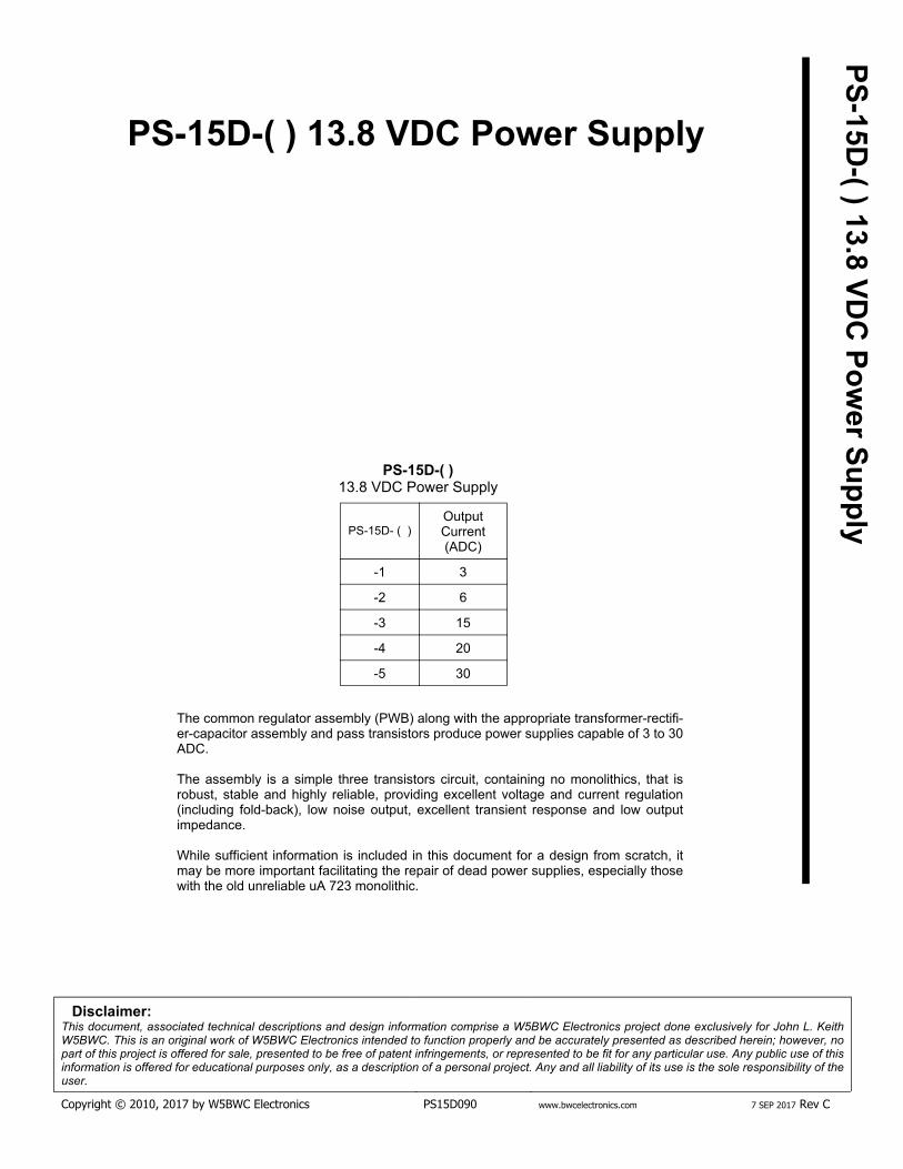
The common regulator assembly (PWB) along with the appropriate transformer-rectifi-er-capacitor assembly and pass transistors produce power supplies capable of 3 to 30ADC.
The assembly is a simple three transistors circuit, containing no monolithics, that isrobust, stable and highly reliable, providing excellent voltage and current regulation(including fold-back), low noise output, excellent transient response and low outputimpedance.
While sufficient information is included in this document for a design from scratch, itmay be more important facilitating the repair of dead power supplies, especially thosewith the old unreliable uA 723 monolithic.
• Designed specifically for continuous, unattended charging of a secondary battery or as astand-alone continuous duty, high reliability power supply. See warnings this page andnext.
• Excellent for powering remote systems and intended to operate in or near RF fields suchas those in the proximity of an Amateur Radio transmitting antenna.
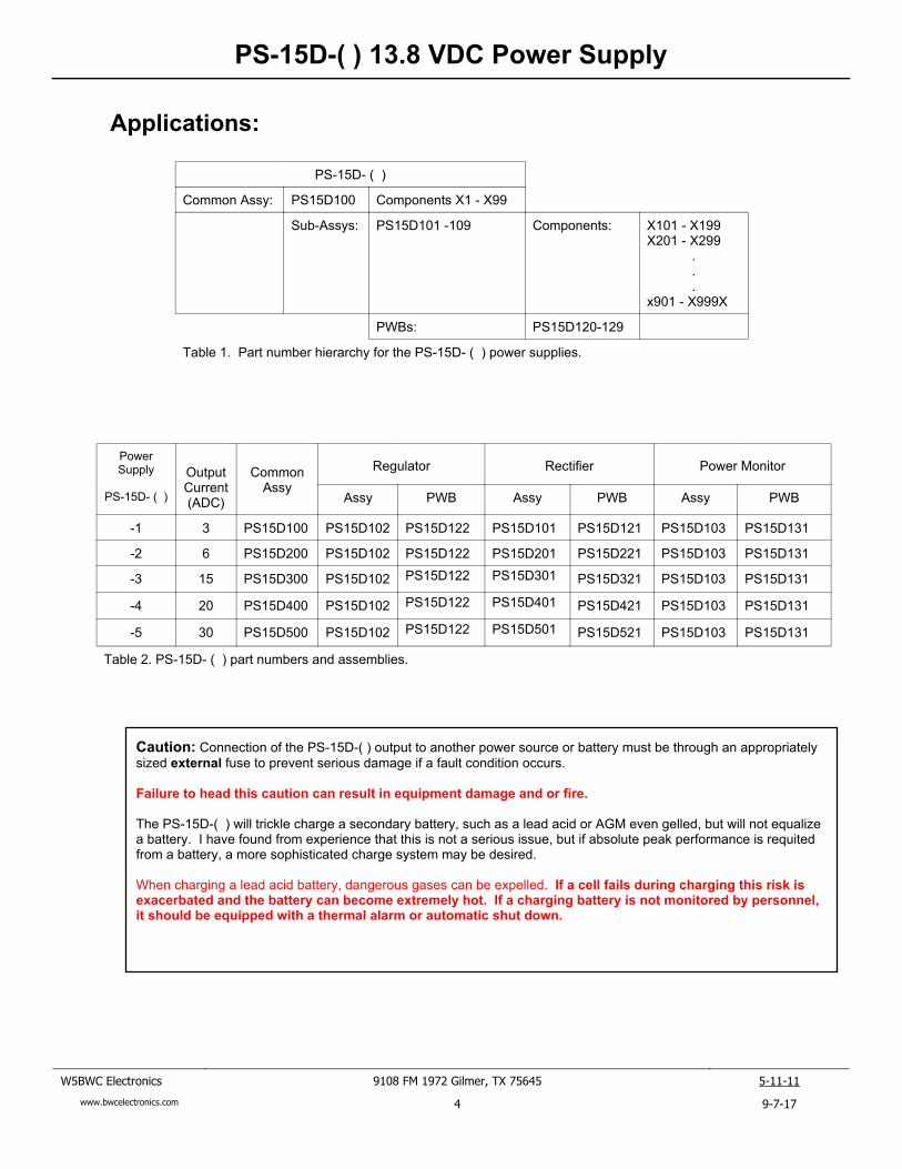
• Intended as the AC power supply of a DC power system using a Monitor & Control suchas the MC-20A-1 Power Monitor which will provide a complete system for under voltagedisconnect, over voltage shutdown, and DC buss monitoring.
Features
• no minimum load
• excellent voltage regulation
• excellent load step response
• very low ripple and noise DC output
• adjustable output voltage
• very low reverse leakage current (drawn from thebattery during AC off conditions)
• load sharing that does NOT require series diodes
• fused in both AC and DC sections
• output reverse voltage protection
· output transient over voltage protection
• RFI/EMI immune output
• RFI/EMI input filter on AC line
• status indicator that allows two LEDs to indicatethat AC power is providing the DC output or thatthe secondary battery is providing the DC output.
(with PS15D103 Buss Status Indicator)
• 100% duty cycle output at ambient temperaturesup to +40 oC
· simple rugged circuit with no high voltage switch-ing or noise generation that requires complex filter-ing and shielding
· excellent for resurrecting non-operational commer-cial power supplies
Caution: Connection of the PS-15D-( ) output toanother power source or battery must be throughan appropriately sized external fuse to preventserious damage if a fault condition occurs.
Failure to head this caution can result inequipment damage and or fire.
Figure 1. Typical construction for PS-15D-4, front side view. Figure 2. Typical construction for PS-15D-4, rear side view.
Caution: Connection of the PS-15D-( ) output to another power source or battery must be through an appropriatelysized external fuse to prevent serious damage if a fault condition occurs.
Failure to head this caution can result in equipment damage and or fire.
The PS-15D-( ) will trickle charge a secondary battery, such as a lead acid or AGM even gelled, but will not equalizea battery. I have found from experience that this is not a serious issue, but if absolute peak performance is requitedfrom a battery, a more sophisticated charge system may be desired.
When charging a lead acid battery, dangerous gases can be expelled. If a cell fails during charging this risk isexacerbated and the battery can become extremely hot. If a charging battery is not monitored by personnel,it should be equipped with a thermal alarm or automatic shut down.
Size 2.30” X 2.75” (58.42mm X 69.85mm)1.05” (26.67mm) tallest component
Material 0.063” (1.60mm) FR-4 fire retardant glass-epoxy1 oz copper clad with tin plate
Mounting Designed to mount on the Output terminals of the power supply with 6-32 screws
Input Voltage 40 VDC (max), no minimum - stable from operational to drop out Limited by 2N5962
Output Current For -1 and -2 (up to 6 ADC) R208 can be board mounted. It is recommended for -3 thru -5(15 to 30 ADC) R208 be mounted externally - see Figure 17 for details
Strapping Options See text and Figure 17 for S201 strapping information - allows accurate current monitoringwith externally mounted R208
Volt and Amp Meter See text for appropriate selection of R215 thru R217 for scaling of external meters
Output VoltageAdjustment
11 to 15 VDC (nominal)12 to 14 VDC (worst case)
Designed for 12 to13.8 VDC
Output VoltageRegulation
Better than 0.10% (~13.8 mV) for load changes from no-load to rated output currentBetter than 0.10% for line changes from maximum to drop out(Both slightly dependent upon transformer-rectifier-capacitor assembly)
Measured at theoutput terminals
Output Voltage Tem-perature Coefficient
Less than 0.04%/oC (nominal)
Current Limit See text and fold-back current limiting equations for details - typically on-set of current limitis 15% above rated output current, folding back to 30% of rated output current into a short
Current Limit Temper-ature Coefficient
Less than 0.6%/oC (nominal)
Pass Transistor Drive 0 to 3 mA with 15V compliance Note 2.
Regulator Current < 4 mA (excluding 100 Ω base resistor on -2 thru -5)
Size 0.95” X 0.95” (24.13mm X 24.13mm)
Material 0.063” (1.60mm) FR-4 fire retardant glass-epoxy1 oz copper clad with tin plate
Mounting Designed to mount on the leads of panel mounted LEDs
Input Voltage 15 to 30 VAC from rectifier transformer10 to 15 VDC from DC Buss
Indicators Green LED indicates AC power ON - works correctly even with battery inputYellow LED indicates DC power ON without AC power present (with battery back-up)
Characteristics: PS15D103 Buss Status Indicator Assembly
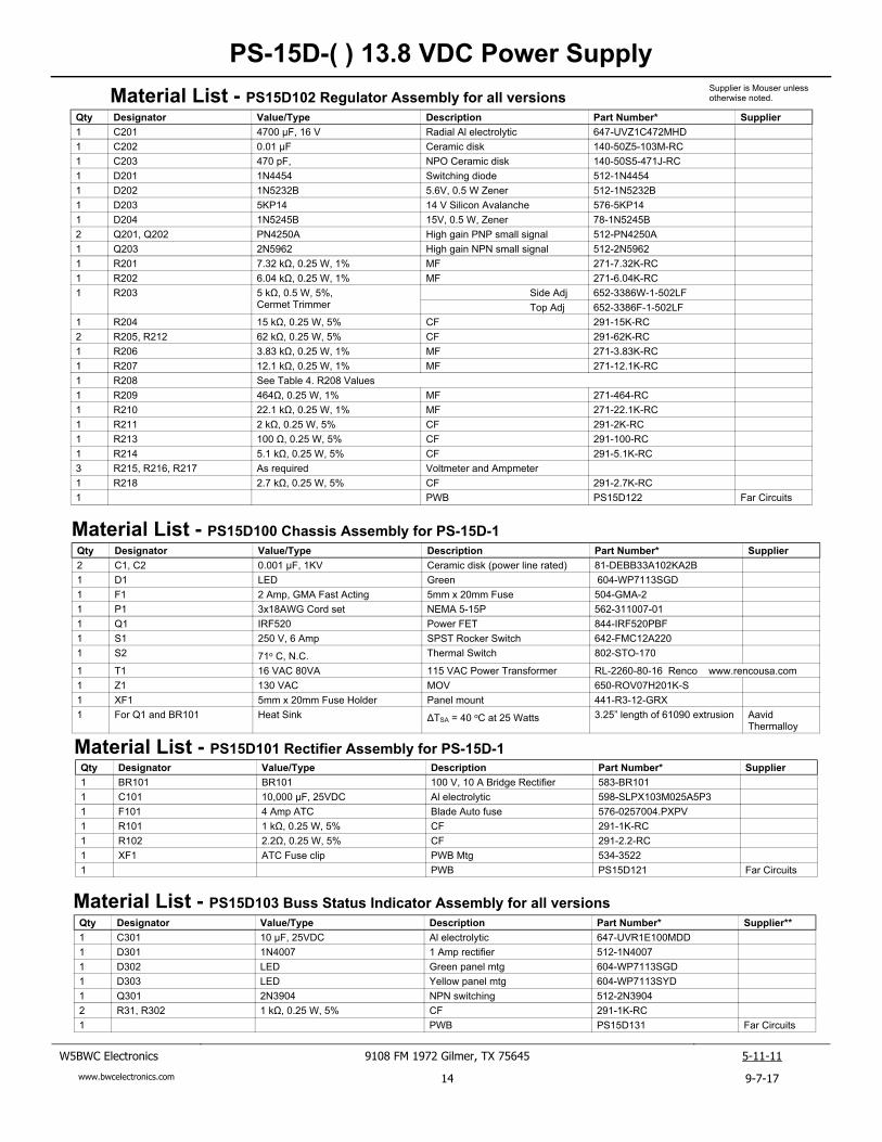
Notes:1. Characteristics apply to PS15D102 assembly with an external pass transistor - see PS-15D-1 thru -5 for specific details.2. Designed specifically to drive the high gate capacitance of a power FET, but also stable driving a bipolar darlington3. PS15D103, Buss Status Indicator, introduces a very small 60Hz component into the DC output.4. Current limit is a function of output voltage - see Figures 8 and 9 for current limit vs output voltage.5. Initial current limit is the current at which the output voltage drops 1% and the fold back current is into a load resistance that produces < 1 VDC output.
Line Regulation 105 to 125 VAC Line13.80 VDC OutputIO = 0 to Rated Full Load at any fixed level
< 0.10% Measured at the output ter-minals
Load Regulation 117.0 VAC Line13.80 VDC OutputΔIO = 0 to Rated Full Load
< 0.10% Measured at the output ter-minals
Ripple and Noise 117.0 VAC Line13.80 VDC OutputIO = 0 to Rated Full Load
<500 µV RMSNote 3.
Output Impedance 117.0 VAC Line DC to 1 kHz13.80 VDC Output 1 kHz to 10 kHzIO = 0 to Rated Full Load 10 kHz to 100 kHz
< 0.005 Ω< 0.005 to 0.035 Ω< 0.035 Ω
See Figure 4.
Output VoltageTemperatureCoefficient
117.0 VAC Line13.80 VDC OutputIO = 0 to Rated Full Load at any fixed level
Less than 0.04%/oC (nomi-nal)
Current Limit Tem-perature Coefficient
117.0 VAC Line13.80 VDC Output
Less than 0.6%/oC (nomi-nal)
Reverse leakagecurrent
0 VAC LineOutput Voltage 12.7 VDC (from external source)
<2 mA
OperatingTemperatureRange
117.0 VAC Line13.80 VDC OutputIO = 0 to Rated Full Load at any fixed level
-20 oC to +40 oC
Fault Protection Input Line fuse GMA Fast acting Fuse selection and use iscritical for component pro-tection as well as facilityprotection.
Input Surge 130 VAC MOV
DC output fuse ATC 32V Blade Fuse
DC output Surge 14 VDC, 5 kW SAD
Duty cycle 117.0 VAC Line13.80 VDC OutputIO = 0 to Rated Full Load
100%
Duty Cycle Warning.The MFJ transformer specified for the -3, 15 ADC version,has 50 oC temperature rise in 15 ADC CCS (commercial continu-ous service) which means with +40 oC ambient the transformer willbe at +90 oC. From a transformer insulation stand point this is ac-ceptable, but I prefer to keep the rise below 40 oC which requiresforced air cooling. As can be seen from the schematic I suggest athermostatically controlled fan, which only runs on demand improv-ing reliability and reducing noise.
This same transformer is specified for the -4, 20 ADC versionwhere the fan is required for CCS 20 ADC service. Without forced
air cooling the transformer rise is in excess of 77 oC - totally unacceptable.
MFJ advertises this transformer for 30ADC output which it is capable of. Asfor as low line and peak current this transformer is fine and seems to be
MFJ 406-3800 Transformer ICAS de-rating
DC OutputCurrent
DutyCycle
Conditions
15 ADC 100% Natural convection cooling and core rise of 50 oC
20 ADC 100% Forced air cooling sufficient to contain core rise.
20 ADC 50% Natural convection cooling and core rise of 50 oCDwell time (full load) of 10 minutes maximum
30 ADC 25% Natural convection cooling and core rise of 50 oCDwell time (full load) of 5 minutes maximum
Figure 4. Output Impedance. Nominal is the expected performance, but is dependent uponactual construction techniques and components. Plotted data from engineering prototypes.
Characteristics: Typical performance and engineering prototype data.
Figure 5. PS-15D-1 Transient Response of engineeringprototype.
Figure 6. PS-15D-2 Transient Response of engineeringprototype.
Figure 7. Transient Response and Output Impedance measured using aterminal mounted FET with low inductance copper straps. For transientresponse, the FET is driven with a pulse generator - VGS and the pulseamplitude are adjusted for the desired current pulse. For output imped-ance, the FET is driven with a signal generator and VGS is set for 1 ADCbias current - measured as 1 Volt across the 1 Ohm source resistor.
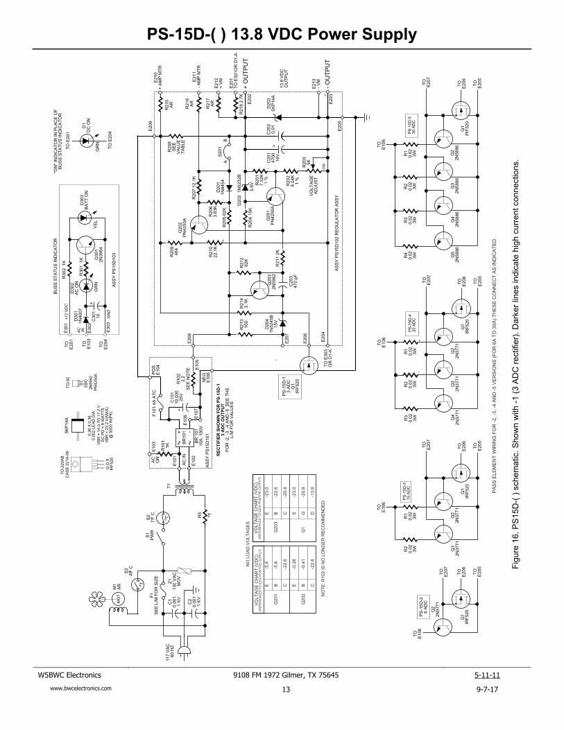
Input AC power is supplied through fuse, F1, power switch, S1,and thermal switch, S2, to the primary winding of T1. To reduceincoming RFI each AC line input is bypassed to ground with a0.001 µF, 1 kV capacitor. Caution: these small capacitorsform a voltage divider between the hot and common lineinputs. If the power line ground is not in tact, this causes thechassis (and output) to float up to approximately 60 VAC.Be sure incoming AC power is supplied through a NEMA5-15P cord set in good condition and properly connected.
The fuse size is determined by the output current rating - see“Characteristics” for actual values. Proper fuse size is essen-tial for protection of the rectifiers. The input fuse does morethan protect wiring and related components from excessive rmscurrent. As importantly, it protects the rectifiers from excessivepeak energy that is described as I2t - the “Joule integral”, itassists in lightning induce current and output over-voltage pro-tection when D203 avalanches. Do NOT dismiss the fuseselection as a trivial matter - it is important to install thecorrect size and type fuse.
The thermal switch is heat sink mounted providing thermal shutdown during fault conditions or excessive ambient temperature.Input surge protection is provided by Z1, a 130 VAC MOV (metaloxide varistor) . In-rush current protection for the higher currentversions is provided by R1, a NTC (negative temperature coeffi-cient) thermistor.
Rectifier and Filter
Transformer, T1, and the rectifier/filter assembly are selectedbased on the output current. Either full wave bridge or full waveCT rectifiers may be used, see Figure 3. Topology and compo-nent selection for custom designs can be made using the “Rec-tifier Design and Analysis” article and free spread sheetcalculator on bwcelectronics.com. PWB assemblies can beused for the lower current versions, but chassis mounted compo-nents are recommended for the higher current versions.
Voltage and Current Regulation
The regulator is a low side, low-drop-out circuit. Several of thisdesign’s benefits are; grounded pass transistor cases, functionalwith low differential voltages, drive voltage is less than outputvoltage - thus no boast winding required, high transconductance,and inherently self starting even with transient conditions duringpower up.
For the 3 ADC version, only a single IRF520 power FET isrequired external to the regulator assembly. A small gate voltagechange on Q1 will result in a large output current change, sovoltage regulation is easy to achieve for varying load (or line)conditions.
Q203 provides a high gain (hFE of 600 to 1400) and inversion asthe final stage of the control circuitry. C203 provides phaseretardation to stabilize the control loop. R214 provides turn-on
bias for Q1 thus ensuring start up with any sequence of ACpower on/off, load condition, or during intermittent AC powerfailures. Q203 under, feedback control, draws the proper currentthrough R214 to establish and maintain loop control.
Q203’s base drive is either from Q201 or Q202 through R211.R211 only serves to protect Q203 in a fault condition where apath from the negative input directly to the positive input couldestablish its’ self through Q203,Q201 and D202.
Q201 and Q202 are high gain (hFE of 250 to 700) PNP inputstages for the control loop. Q201 provides voltage regulation bycomparing a fraction of the output voltage (through R201, R202and R203) to the reference voltage of D202, a 1N5232B zenerdiode.
The negative voltage coefficient of Q201 BE junction is partiallycompensated for by the positive voltage coefficient of D202,thus providing some temperature stabilization. Note D202 isbiased by the output voltage, thus effecting a constant currentfeed and so eliminates input voltage fluctuations from effectingthe reference voltage.
Voltage or current control automatically switches between Q201and Q202. If the output current is below the preset value, Q202will be turned off and Q201 will control the loop (voltage regula-tion) as described previously.
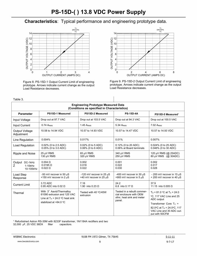
However, when output current becomes sufficient to bias onQ202, it will begin to conduct and take control of the loop(current regulation). R209 and R210 provide an emitter bias thatis a function of the output voltage. This emitter bias will lower theeffective current limit as the output voltage drops and thereforeeffects a current fold-back which protects the pass transistors.Note also, setting the output voltage lower than 13.8 VDC lowersthe initial output current limit by the ratio shown in the fold backcurves, see Figures 8 and 9 .
D201 is used to bias Q202 up slightly so that only 300 mV isrequired across the sense resistor. A secondary benefit of D201is to provide some temperature compensation for Q202’s BEjunction. R206, R207 and R208 set the initial current limit leveland R209 and R210 set the fold-back current level (but withinterdependence). See Figure 17. for additional details.
R208 is mounted on the Regulator Assembly for -1 and -2 (3 and6 ADC) but should be externally mounted for -3, -4 and -5. Thehigher current versions can generate sufficient heat in R208 todamage a PWB as well as being too bulky for the PWB.
When R208 is externally mounted, strap S201 should be notused. R208 should be wired conveniently from the DC fuse toE202 (same as S201-B). E209 should then be wired directly tothe (+) end of R208, near the body of the resistor. S201-A iswired directly to the (-) end of R208, again close to the resistorbody. This method of wiring will preserve the accuracy of thecurrent limit and monitoring.
If the Regulator Assembly is not mounted directly on the outputterminals, some loss of regulation may occur due to the wiring
Basic Operation:resistance. Also, the output impedance and surge protectionwill be degraded as the lead length to C201 and D203increases. It is highly recommended that the RegulatorAssembly directly mount onto the output terminals.
An external current meter can be connected to E210 (+) andE211 (-). Resistor values are selected to calibrate the ampmeter over the 3 to 30 Amp range. The use of both R215and R216 will protect the meter and wiring from the highcurrent potential of the output. For a hi-Z DPM a third resistoris added from E210 to E211 providing the correct scaling forthe desired range.
An external voltmeter can be connected to E212 (+) andE213 (-). R217 provides scaling and current limit protection.If a voltage divider is required, e.g. for a DPM, a shuntresistor is added from E212 to E213, with values selected forthe required scaling.
Pass transistor(s)
Refer to the schematic to see pass transistors details for thedifferent output currents. The number and type of transistorsare selected to ensure each version has sufficient margin tomeet the output current and current limit specifications. If thismaterial is being used to rework a dead Amateur Radiopower supply, be sure to pay attention to the thermal design.A lot of products are specified using a very liberal interpreta-tion of ICAS (intermittent commercial and amateur service),but in continuous duty and high ambient temperature willactually not perform anywhere near the advertised specifica-tion.
Thermal
Probably the most difficult task associated with the PS-15D,or any linear power supply, is managing the thermal design.Most Amateur Radio power supplies use some form of ICASrating and few if any have a true CCS rating advertised.
Thermal equivalency can be used to predict ICAS perfor-mance if CCS is known (and vice a versa). Equation 1.shows the relationship mathematically. Basically when theduty cycle is reduced from 100% to 50%, the equivalentheating is reduced to 70.7% - not 50%.
This thermal equivalency means that a power supply ratedat 35 ADC ICAS should operate at 25 ADC CCS. However,a necessary detail is often omitted in advertised specifica-tions, that is, what is the maximum time full-load can beapplied and at what ambient temperature. The maximum “ontime” is a function of the temperature critical components’thermal time constant and the permissible ambient tempera-ture is a function of the design’s thermal margins.
PICAS = PCCS(TON + TOFF)
TON√Equation 1.
The PS-15D-( ) thermal design provides safe operation with heatsink temperatures of +65oC up to +40oC ambient and full 100%CCS. However, +65oC is very HOT (149oF) and unsuitable forhuman contact. Forced air cooling is highly recommended for the -3,-4 and -5 versions.
Also, beware that many commercial power supplies sold into theretail Amateur Radio market will exceed +80oC at full load (evenwithin the advertised specifications). The success of these salesmust result from the fact many applications are for SSB or otherintermittent loads. But, if your application is FM, digital or other “brickon the key” modes, you are likely to have problems with some ofthese “ICAS” rated power supplies.
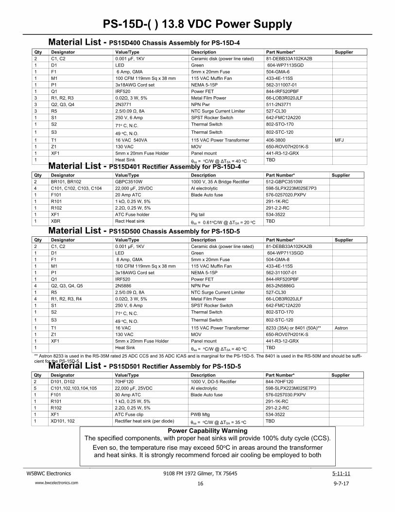
Material List - PS15D400 Chassis Assembly for PS-15D-4
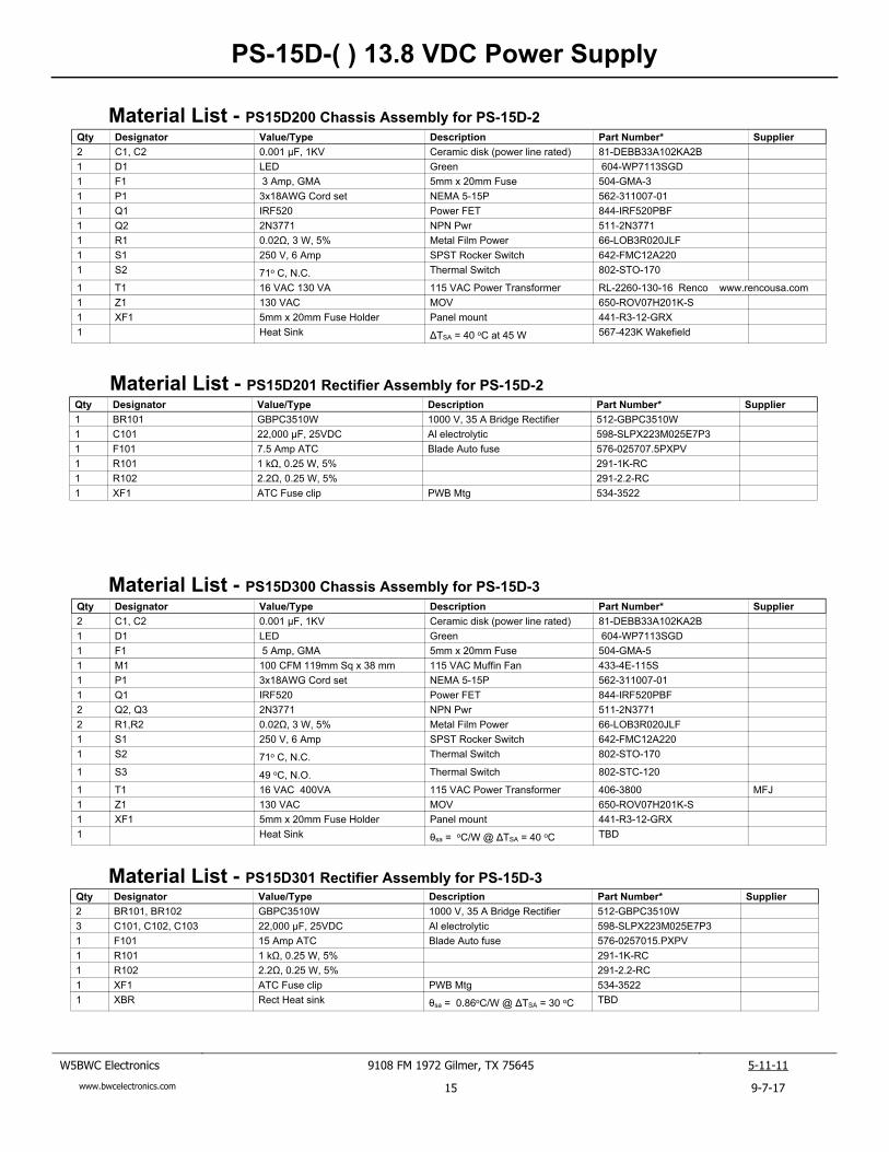
Material List - PS15D401 Rectifier Assembly for PS-15D-4Qty Designator Value/Type Description Part Number* Supplier2 BR101, BR102 GBPC3510W 1000 V, 35 A Bridge Rectifier 512-GBPC3510W4 C101, C102, C103, C104 22,000 µF, 25VDC Al electrolytic 598-SLPX223M025E7P31 F101 20 Amp ATC Blade Auto fuse 576-0257020.PXPV1 R101 1 kΩ, 0.25 W, 5% 291-1K-RC1 R102 2.2Ω, 0.25 W, 5% 291-2.2-RC1 XF1 ATC Fuse holder Pig tail 534-35221 XBR Rect Heat sink θsa = 0.61oC/W @ ΔTSA = 20 oC TBD
Qty Designator Value/Type Description Part Number* Supplier2 C1, C2 0.001 µF, 1KV Ceramic disk (power line rated) 81-DEBB33A102KA2B1 D1 LED Green 604-WP7113SGD1 F1 8 Amp, GMA 5mm x 20mm Fuse 504-GMA-81 M1 100 CFM 119mm Sq x 38 mm 115 VAC Muffin Fan 433-4E-115S1 P1 3x18AWG Cord set NEMA 5-15P 562-311007-011 Q1 IRF520 Power FET 844-IRF520PBF4 Q2, Q3, Q4, Q5 2N5886 NPN Pwr 863-2N5886G1 R5 2.5/0.09 Ω, 8A NTC Surge Current Limiter 527-CL304 R1, R2, R3, R4 0.02Ω, 3 W, 5% Metal Film Power 66-LOB3R020JLF1 S1 250 V, 6 Amp SPST Rocker Switch 642-FMC12A2201 S2 71o C, N.C. Thermal Switch 802-STO-170
1 S3 49 oC, N.O. Thermal Switch 802-STC-120
1 T1 16 VAC 115 VAC Power Transformer 8233 (35A) or 8401 (50A)** Astron1 Z1 130 VAC MOV 650-ROV07H201K-S1 XF1 5mm x 20mm Fuse Holder Panel mount 441-R3-12-GRX1 Heat Sink θsa = oC/W @ ΔTSA = 40 oC TBD
** Astron 8233 is used in the RS-35M rated 25 ADC CCS and 35 ADC ICAS and is marginal for the PS-15D-5. The 8401 is used in the RS-50M and should be suffi-cient for the PS-15D-5.
Material List - PS15D500 Chassis Assembly for PS-15D-5
Power Capability WarningThe specified components, with proper heat sinks will provide 100% duty cycle (CCS).
Even so, the temperature rise may exceed 50oC in areas around the transformerand heat sinks. It is strongly recommend forced air cooling be employed to both
IO = Output current (general expression)ION = Output current where Limiting startsIFB = Output current with VO folded back to zeroRS = Current sense resistor in OhmsVON = Nominal full-load voltage prior to currentlimitingVFB = Output voltage at IFB
VBE @ IB VR @ IF
I1 = desired total current thru Ra + RbI2 = desired total current thru Rc + Rd
( I1 and I2 need to be much largerthan IB and IE, which are quitesmall, but as small as possible tominimize reverse current)
IB, IE << I1 or I2 and I1 << IF
α = β(VO + IONRS) - IONRS + VBE
VR
Ra = αVR
I1
Rd =VO(1 - β)
I2Rc = Rd
1/β - 1
Rb = Ra(1/α - 1)
β =RS(ION - IFB)
VON - VFB + RS(ION - IFB)
IO = VBE - αVR + βVO
RS(1 - β)
IO vs VOValid only foractive currentlimiting
β = RcRc + Rd
IO =VBE - αVR
RS(1 - β) - βRL
IO vs RL
Valid only foractive currentlimiting and RL< VON/ION
α = RRa + Rb
Figure 17. Current limit equations.
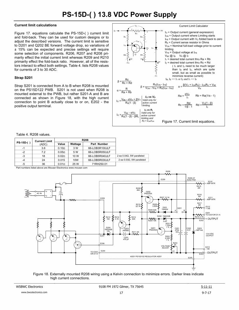
Current limit calculations
Figure 17. equations calculate the PS-15D-( ) current limitand fold-back. They can be used for custom designs or toadjust the described versions. The current limit is sensitiveto D201 and Q202 BE forward voltage drop, so variations of± 15% can be expected and precise settings will requiresome selection of components. R206, R207 and R208 pri-marily effect the initial current limit whereas R209 and R210primarily effect the fold-back ratio. However, all of the resis-tors interact to effect both settings. Table 4. lists R208 valuesfor currents of 3 to 30 ADC.
Strap S201
Strap S201 is connected from A to B when R208 is mountedon the PS15D122 PWB. S201 is not used when R208 ismounted external to the PWB, but rather S201-A and B areconnected as shown in Figure 18, with the high currentconnection to point B actually close to or on, E202 - thepositive output terminal.
Table 4. R208 values.
PS-15D-( ) Current Limit(ADC)
R208Value Wattage Part Number
-1 3.6 0.10Ω 3 W 66-LOB3R100JLF-2 7.2 0.05Ω 5 W 66-LOB5R050JLF-3 18 0.02Ω 10 W 66-LOB5R040JLF 2 ea 0.04Ω, 5W paralleled
-4 24 0.015 10W 66-LOB5R030JLF 2 ea 0.03Ω, 5W paralleled
-5 36 0.01Ω 25 W 71RH250.01Part numbers listed above are Mouser Electronics www.mouser.com
Figure 18. Externally mounted R208 wiring using a Kelvin connection to minimize errors. Darker lines indicatehigh current connections.
Figure 19. PS-15D-1 view inside chassis. Chassis formedfrom 0.040 5052-H32 sheet aluminum on shop brake. Bud orother manufacturer’s chassis can be substituted.
Typical construction of the PS-15D-( ) power supplies as new and refurbished.
T1
Z401
C402
C401F401
PS15D103AC O
N
BATT
ON
PS15D101
PS15D102Q1
Figure 20. PS-15D-1 top view . Heat sink mounts on chassiswhich has a cut-out for Q1 to mount directly on the heat sink.
Figure 21. PS-15D-1side view showing the Buss Status LEDs.This particular power supply provides float charge and regula-tion for an entry gate where the Buss Status is adapted toprovide local and remote status as well as to control the enclo-sure’s ventilation fan.
R208
F101
R203Voltage
Figure 22. Inside view of PS-15D-5 reworked into anAstron RS-35M power supply. Transformer, rectifiers,filter capacitors and heat sink were re-used with thePS15D102 regulator assembly.
Figure 23. Close-up view of PS15D102 mounted oncopper brackets to the output terminals of the RS-35Mrefurbished into a PS-15D-5.
As of September 2017, a few hundred PS15D102 regulatorboards have been built and installed. Of these I have onlyhad a few request for help (which I am glad to provide).
In all cases, difficulties have been traced to wiring errors, withthe exception of D203, which can fail if a prolonged overvoltage is present at the output (which has occurred due towiring errors). This TVS is present to provide reverse voltageprotection, protect the load and regulator from high voltageinductive spikes resulting from switching an inductive loadand induced EM transients (such as near-by lightning).
The original implementation indicated the TVS would openF101 for an extended over-voltage, but for different sizes andtypes of fuses, this can not be expected. For extendedover-voltage protection, the MC-20A-1 DC Buss Monitor andControl or an SCR crowbar , see Figure 24., is recommend-ed.
Figure 25. is the schematic of one Astron RS-35M I reworkedfor a friend. I have received comments this helps understandthe board implementation when reworking Astron powersupplies. Note however, Astron power supply models differone from another depending upon when they were manufac-tured and so may not be represented by this particularrefurbish.
Also notice the 2.2Ω, R102 is no longer recommended. Itspurpose was to protect the circuit board, but if it opens theregulator looses control which is a bigger problem.
4. Q2 THRU Q5 COLLECTORS SHOULD WIRE TO E203 (OUTPUTNEGATIVE TERMINAL) WITH APPROX EQUAL LENGTHS OF AWG18 (MIN) WIRE.
5. Q2 THUR Q5 SHOULD BE MOUNTED TO THE HEAT SINK USINGAN INSULATOR KIT AND THERMAL COMPOUND WITHOUTSOCKETS.
6. Q1 SHOULD BE MOUNTED TO THE CHASSIS USING A TO-220INSULATOR KIT AND THERMAL COMPOUND.
7. ASTRON PARTS ARE REPRESENTATIVE OF OLDER UNITS -BEWARE NEWER VERSION MAY HAVE DIFFERENT PARTS.
8. IN PARTICULAR, R215 THRU R217 ARE TEST SELECTED BASEDON THE METER(S) PRESENT. THE CURRENT SENSE IS 10mV/AMP.
9. D203 PROVIDES OV, TRANSIENT CLAMPING AND REV VOLTAGEPROTECTION. ANY EXTERNAL POWER SOURCE CONNECTEDTO THE OUTPUT MUST BE THROUGH A FUSE OF NOT MORETHAN 30 AMPS.
10. F2 MUST BE NO MORE THAN 30 AMPS TO ENSURE D203'S i2tRATING IS NOT EXCEEDED.
(NOTE 3)
(NOTE 4)
(NOTE 7,8)
(NOTE 9)
(NOTE 7,8)
(NOTE 10)
S3
G
D
S
Figure 25. Schematic of an Astron power supply refurbished with the PS15D102.
FAQ
1. The regulator has NO minimum load requirement.
2. Q1-S connects to the negative side of the rectifier/filter when it is theonly pass element in use (no NPN pass transistors).
3. Q1-S connects to E207 when external NPN pass transistors are used.
4. S201 is wired from S201-A to S201-B if R208 is mounted on the PCB.
5. S201-A is wired to the output terminal side of R208 when anexternal resistor is used. S201-B is left unused.
6. The PS15D102 is NOT a drop in replacement for Astronboards.
7. The PS15D102 is for refurbishing Astron power supplies -meaning it is not a drop-in replacement. For instance, thepass transistors are emitter followers in most Astron circuitsbut are common emitter configuration in the refurbish.
8. The PS15D102 is a very robust circuit. Most wiring errors donot damage the regulator itself. However, Q1 and D203 canbe damaged by miswiring.
9. The PS15D102 regulator assembly does not have to bemounted on the output terminals. Best transient responseand regulation are achieved by doing so, but for poweringmost electronic equipment, such as HF transceivers, it is ofless importance.
10. Basic electronics training, soldering skills and ability to readschematics are required to refurbish a power supply.
11. For instructional purposes, the PS15D102 can be used tobuild the PS-15D-1 (basic 3A power supply). Even so, it isstrongly recommended you have an instructor or mentor onhand.
12. I can provide tech support but I am not capable of providingcorrespondence electronic technician training.
13. This document contains a lot of information and deservescareful study if you have problems, and I likely will refer youto it when you request tech support. Even so, fell free to askfor help if you get stumped.
14. Component changes; D203 is now 1.5KE18 and Q201,Q202 are 2N5087 (still can use PN4250A if you can findthem). Even 2N3906 can be used with slight loss of perfor-mance.