PSoC 6 MCU: CYS0644xxZI-S2D44 Datasheet PSoC 64 Standard Secure MCU-AWS PRELIMINARY Cypress Semiconductor Corporation • 198 Champion Court • San Jose, CA 95134-1709 • 408-943-2600 Document Number: 002-28690 Rev. *B Revised June 12, 2020 General Description PSoC ® 6 MCU is a high-performance, ultra-low-power, and secure MCU platform, purpose-built for IoT applications. The PSoC 64 AWS Standard Secure MCU product line, based on the PSoC 6 MCU platform, features out-of-box security functionality, providing an isolated root-of-trust with true attestation and provisioning services. In addition, it delivers a pre-configured, PSA level-2 compliant secure execution environment, which is custom-built to support the Amazon FreeRTOS ecosystem. PSoC 64 also includes a rich execution environment for application development, with Amazon FreeRTOS support that communicates with the secure execution environment. Features 32-bit Dual CPU Subsystem Note: In PSoC 64 the Cortex M0+ is reserved for system functions, and is not available for applications. ■ 150-MHz Arm ® Cortex ® -M4F (CM4) CPU with single-cycle multiply, floating point, and memory protection unit (MPU) ■ 100-MHz Cortex-M0+ (CM0+) CPU with single-cycle multiply and MPU ■ User-selectable core logic operation at either 1.1 V or 0.9 V ■ Active CPU current slope with 1.1-V core operation ❐ Cortex-M4: 40 µA/MHz ❐ Cortex-M0+: 28 µA/MHz ■ Active CPU current slope with 0.9-V core operation ❐ Cortex-M4: 27 µA/MHz ❐ Cortex-M0+: 20 µA/MHz ■ Three DMA controllers Memory Subsystem ■ 1856-KB application flash, 32-KB auxiliary flash (AUXflash), and 32-KB supervisory flash (SFlash); read-while-write (RWW) support. Two 8-KB flash caches, one for each CPU ■ 920-KB SRAM with three independent blocks for power and data retention control ■ One-time-programmable (OTP) 1-Kb eFuse array Amazon FreeRTOS Platform System Architecture (PSA) Integration ■ Out-of-box solution for enabling Amazon FreeRTOS (AFR) with Arm Platform Service Architecture (PSA) Level-2 Compliance ■ Pre-built Trusted Firmware-M (TF-M) Secure Processing Environment (SPE) binary built for the PSoC 64 Standard Secure MCU ■ Amazon FreeRTOS API-level integration for TLS, firmware update, and secure storage Hardware-Based Root-of-Trust (RoT) ■ RoT based on immutable boot-up code, flash content hash, and Cypress public key that ensures firmware integrity prior to provi- sioning ■ Supports trusted RoT handover to maintain chain of trust and establish OEM trust anchor for secure boot ■ Device generates a unique device ID and a device secret key during the provisioning process, which can be used for attes- tation and signing Immutable Secure Boot Support ■ Flexible chain of trust can use different signatures for different images ■ ECC-based image signature validation Cypress Secure Bootloader ■ Open Source MCUBoot [1] based bootloader optimized for PSoC 64 ■ Pre-built bootloader binary capable of validating, launching and updating signed user application images ■ Tightly integrated with provisioned debug and boot policies to inherit and implement security policies Low-Power 1.7-V to 3.6-V Operation ■ Six power modes for fine-grained power management ■ Deep Sleep mode current of 7 µA with 64-KB SRAM retention ■ On-chip DC-DC buck converter, <1 µA quiescent current ■ Backup domain with 64 bytes of memory and real-time clock Flexible Clocking Options ■ On-chip crystal oscillators (16 to 35 MHz, and 32 kHz) ■ Two phase-locked loops (PLLs) for multiplying clock frequencies ■ 8-MHz internal main oscillator (IMO) with ±2% accuracy ■ Ultra-low-power 32-kHz internal low-speed oscillator (ILO) ■ Frequency-locked loop (FLL) for multiplying IMO frequency Quad-SPI (QSPI)/Serial Memory Interface (SMIF) ■ Execute-In-Place (XIP) from external quad SPI flash ■ On-the-fly encryption and decryption ■ 4-KB cache for greater XIP performance with lower power ■ Supports single, dual, quad, dual-quad, and octal interfaces with throughput up to 640 Mbps Note 1. For details, refer to https://mcuboot.com/.
Transcript
PSoC 6 MCU: CYS0644xxZI-S2D44Datasheet
PSoC 64 Standard Secure MCU-AWSPRELIMINARY
Cypress Semiconductor Corporation • 198 Champion Court • San Jose, CA 95134-1709 • 408-943-2600Document Number: 002-28690 Rev. *B Revised June 12, 2020
General Description
PSoC® 6 MCU is a high-performance, ultra-low-power, and secure MCU platform, purpose-built for IoT applications. The PSoC 64AWS Standard Secure MCU product line, based on the PSoC 6 MCU platform, features out-of-box security functionality, providing anisolated root-of-trust with true attestation and provisioning services. In addition, it delivers a pre-configured, PSA level-2 compliantsecure execution environment, which is custom-built to support the Amazon FreeRTOS ecosystem. PSoC 64 also includes a richexecution environment for application development, with Amazon FreeRTOS support that communicates with the secure executionenvironment.
Features32-bit Dual CPU Subsystem
Note: In PSoC 64 the Cortex M0+ is reserved for systemfunctions, and is not available for applications.
150-MHz Arm® Cortex®-M4F (CM4) CPU with single-cycle multiply, floating point, and memory protection unit (MPU)
100-MHz Cortex-M0+ (CM0+) CPU with single-cycle multiply and MPU
User-selectable core logic operation at either 1.1 V or 0.9 V
Active CPU current slope with 1.1-V core operation Cortex-M4: 40 µA/MHz Cortex-M0+: 28 µA/MHz
Active CPU current slope with 0.9-V core operation Cortex-M4: 27 µA/MHz Cortex-M0+: 20 µA/MHz
13 run-time configurable serial communication blocks (SCBs) Eight SCBs: configurable as SPI, I2C, or UART Four SCBs: configurable as I2C or UART One Deep Sleep SCB: configurable as SPI or I2C
USB Full-Speed device interface
Two independent SD Host Controller/eMMC/SD controllers
Audio Subsystem
Two pulse density modulation (PDM) channels and two I2S channels with time division multiplexed (TDM) mode
12-bit 2-Msps SAR ADC with differential and single-ended modes and 16-channel sequencer with result averaging
Two low-power comparators available in system Deep Sleep and Hibernate modes
Built-in temperature sensor connected to ADC
Up to 102 Programmable GPIOs
Two Smart I/O™ ports (16 I/Os) enable Boolean operations on GPIO pins; available during system Deep Sleep
Programmable drive modes, strengths, and slew rates
Six overvoltage-tolerant (OVT) pins
Capacitive Sensing
Cypress CapSense® sigma-delta (CSD) provides best-in-class signal-to-noise ratio (SNR), liquid tolerance, and proximity sensing
Enables dynamic usage of both self and mutual sensing
Automatic hardware tuning (SmartSense™)
Cryptography Accelerator Hardware acceleration for symmetric and asymmetric
cryptographic methods and hash functions
True random number generator (TRNG) function
Profiler
Eight counters provide event or duration monitoring of on-chip resources
Packages
124-BGA
Document Number: 002-28690 Rev. *B Page 3 of 76
PRELIMINARY PSoC 6 MCU: CYS0644xxZI-S2D44
Datasheet
Contents
Development Ecosystem ................................................. 4PSoC 6 MCU Resources ............................................. 4ModusToolbox™ IDE and the PSoC 6 SDK ............... 5
Blocks and Functionality ................................................. 6Functional Description..................................................... 8
CPU and Memory Subsystem ..................................... 8System Resources .................................................... 11Programmable Analog Subsystems .......................... 13Programmable Digital ................................................ 14Fixed-Function Digital ................................................ 14GPIO ......................................................................... 16Special-Function Peripherals .................................... 17Secure Boot Functionality ......................................... 21Amazon FreeRTOS PSA Integration Details ............. 23
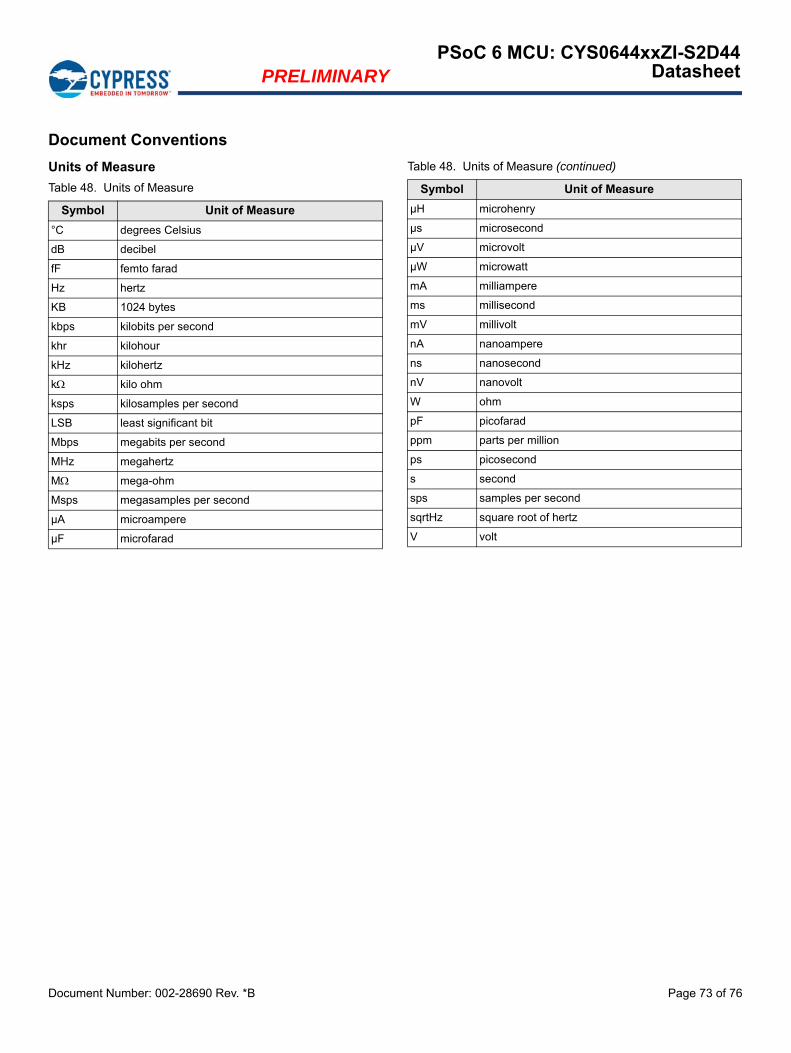
Units of Measure ....................................................... 73Errata ............................................................................... 74Revision History ............................................................. 75Sales, Solutions, and Legal Information ...................... 76
Worldwide Sales and Design Support ....................... 76Products .................................................................... 76PSoC® Solutions ...................................................... 76Cypress Developer Community ................................. 76Technical Support ..................................................... 76
Document Number: 002-28690 Rev. *B Page 4 of 76
PRELIMINARYPSoC 6 MCU: CYS0644xxZI-S2D44
Datasheet
Development Ecosystem
PSoC 6 MCU Resources
Cypress provides a wealth of data at www.cypress.com to help you select the right PSoC device and quickly and effectively integrateit into your design. The following is an abbreviated list of resources for PSoC 6 MCU:
Overview: PSoC Portfolio, PSoC Roadmap
Product Selectors: PSoC 6 MCU
Application Notes cover a broad range of topics, from basic to advanced level, and include the following: AN221774: Getting Started with PSoC 6 MCU AN218241: PSoC 6 MCU Hardware Design Guide AN213924: PSoC 6 MCU Device Firmware Update Guide AN219528: PSoC 6 MCU Power Reduction Techniques AN85951: PSoC 4, PSoC 6 MCU CapSense Design Guide
Code Examples demonstrate product features and usage, and are also available on Cypress GitHub repositories.
Technical Reference Manuals (TRMs) provide detailed descriptions of PSoC 6 MCU architecture and registers.
PSoC 6 MCU Programming Specification provides the infor-mation necessary to program PSoC 6 MCU nonvolatile memory
Development Tools ModusToolbox™ enables cross platform code development
with a robust suite of tools and software libraries CY8CKIT-064S0S2-4343W[1] PSoC 64 Standard Secure
Prototyping Kit: a low-cost hardware platform that enables design and debug of the PSoC 64 CYS0644xxZI-S2D44 product line.
PSoC 6 CAD libraries provide footprint and schematic sup-port for common tools. BSDL files and IBIS models are also available.
Training Videos are available on a wide range of topics including the PSoC 6 MCU 101 series
Cypress Developer Community enables connection with fellow PSoC developers around the world, 24 hours a day, 7 days a week, and hosts a dedicated PSoC 6 MCU Community
Note1. The link will be provided in a later revision.
ModusToolbox is an Eclipse-based development environment on Windows, macOS, and Linux platforms that includes theModusToolbox IDE and the PSoC 6 SDK. The ModusToolbox IDE brings together several device resources, middleware, and firmwareto build an application. Using ModusToolbox, you can enable and configure device resources and middleware libraries, writeC/C++/assembly source code, and program and debug the device.
The PSoC 6 SDK is the software development kit for the PSoC 6 MCU. The SDK makes it easier to develop firmware for supporteddevices without the need to understand the intricacies of the device resources.
For additional details on using the Cypress tools, refer to AN221774: Getting Started with PSoC 6 MCU and the documentation andhelp integrated into ModusToolbox. As Figure 1 shows, with the ModusToolbox IDE, you can:1. Create a new application based on a list of starter applications, filtered by kit or device, or browse the collection of code examples
online.2. Configure device resources in design.modus to build your hardware system design in the workspace.3. Add software components or middleware.4. Develop your application firmware.
Figure 1. ModusToolbox IDE Resources and Middleware
Figure 2 shows the major subsystems and a simplified view of their interconnections. The color coding shows the lowest power modewhere the particular block is still functional (for example, the SRAM is functional down to system Deep Sleep mode).
Flash2048 KB + 32 KB + 32 KB8 KB cache for each CPU
SRAM0512 KB
ROM64 KB
Per
iphe
ral I
nte
rco
nne
ct (
MM
IO,
PP
U)
Pe
riph
eral
clo
ck (
PC
LK)System Resources
Power Clocks
POR
LVD
BOD
OVP
Buck Regulator
WCORTC
IMO
WDT
2x PLL
ECO
ILO
FLL
2x MCWDT
Backup Regs
XRES Reset
PMIC Control
SRAM1256 KB
SRAM2256 KB
4x I2C,UART, or LIN
2x SD Host ControllerSD, SDIO, eMMC
8x I2C, SPI,UART, or LIN
PSoC 64 Standard Secure MCUCYS0644xxZI-S2D44
SystemHibernate Mode
BackupDomain
SystemDeep Sleep Mode
System LP/ULP ModeCPUs Active/Sleep
Color Key:Power Modes and
Domains
Document Number: 002-28690 Rev. *B Page 7 of 76
PRELIMINARYPSoC 6 MCU: CYS0644xxZI-S2D44
Datasheet
This product line has up to 2 MB of flash; however 192 KB is reserved for system usage, leaving 1856 KB for applications. It also hasup to 1 MB of SRAM; however 104 KB is reserved for system usage, leaving 920 KB for applications.
The PSoC 64 devices offer an immutable, RoT-based boot-up process, which allows only signed applications to be booted up. Inaddition, secure user assets such as keys and debug policies can be securely provisioned on the device in an HSM environment andmade immutable. The PSoC 64 line of Secure MCUs also allows for secure root-of-trust based cryptography services which can beaccessed using system calls.
There are three debug access ports, one each for CM4 and CM0+, and a system port. All debug and test interfaces can be permanentlydisabled during final production provisioning to avoid any malicious reprogramming or reading of flash and register contents.
PSoC 6 MCU devices include extensive support for programming, testing, debugging, and tracing both hardware and firmware. Alldevice interfaces can be permanently disabled (device security) for applications concerned about attacks due to a maliciouslyreprogrammed device or attempts to defeat security by starting and interrupting flash programming sequences. All programming,debug, and test interfaces are disabled when maximum device security is enabled. The security level is settable by the user.
Complete debug-on-chip functionality enables full device debugging in the final system using the standard production device. It doesnot require special interfaces, debugging pods, simulators, or emulators. Only the standard programming connections are requiredto fully support debug.
The ModusToolbox Integrated Development Environment (IDE) provides fully integrated programming and debug support for thesedevices. The SWJ (SWD and JTAG) interface is fully compatible with industry-standard third party probes. With the ability to disabledebug features, with very robust flash protection, and by allowing customer-proprietary functionality to be implemented in on-chipprogrammable blocks, PSoC 6 provides a very high level of security.
Document Number: 002-28690 Rev. *B Page 8 of 76
PRELIMINARYPSoC 6 MCU: CYS0644xxZI-S2D44
Datasheet
Functional Description
The following sections provide an overview of the features,capabilities and operation of each functional block identified inthe block diagram in Figure 2. For more detailed information,refer to the following three references.
PDL provides low-level drivers for each resource in the de-vice, and supports the entire PSoC 6 MCU portfolio. PDL isan element of the PSoC 6 SDK, which is installed as part ofModusToolbox. With ModusToolbox installed, you can accessthe PDL API reference manual either from the Documentationtab of the Quick Panel, or you can navigate directly to it at<install_directory>\ModusToolbox_<version>\librar-ies\psoc6sw-<version>\docs. Using PDL should be the pri-mary means of interacting with the PSoC 6 MCU hardware.
Architecture Technical Reference Manual (TRM)
The architecture TRM provides a detailed description of eachresource in the device. This is the next reference to use if it isnecessary to understand the operation of the hardware belowthe software provided by PDL. It describes the architectureand functionality of each resource and explains the operationof each resource in all modes. It provides specific guidanceregarding the use of associated registers.
Register Technical Reference Manual
The register TRM provides a complete list of all registers inthe device. It includes the breakdown of all register fields,their possible settings, read/write accessibility, and defaultstates. All registers that have a reasonable use in typical ap-plications have functions to access them from within PDL.Note that ModusToolbox and PDL may provide software de-fault conditions for some registers that are different from andoverride the hardware defaults.
CPU and Memory Subsystem
PSoC 6 has multiple bus masters, as Figure 2 shows. They are:CPUs, DMA controllers, QSPI, USB, SD Host Controllers, and aCrypto block. Generally, all memory and peripherals can beaccessed and shared by all bus masters through multi-layer ArmAMBA high-performance bus (AHB) arbitration. Accessesbetween CPUs can be synchronized using an inter-processorcommunication (IPC) block.
CPUs
There are two Arm Cortex CPUs:
The Cortex-M4 (CM4) has single-cycle multiply, a floating-pointunit (FPU), and a memory protection unit (MPU). It can run at upto 150 MHz. This is the main CPU, designed for a short interruptresponse time, high code density, and high throughput.
CM4 implements a version of the Thumb instruction set basedon Thumb-2 technology (defined in the Armv7-M ArchitectureReference Manual).
The Cortex-M0+ (CM0+) has single-cycle multiply, and an MPU.It can run at up to 100 MHz; however, for CM4 speeds above 100MHz, CM0+ and bus peripherals are limited to half the speed ofCM4. Thus, for CM4 running at 150 MHz, CM0+ and peripheralsare limited to 75 MHz.
CM0+ is the secondary CPU; it is used to implement system callsand device-level security, safety, and protection features. CM0+provides a secure, uninterruptible boot function. This guaranteesthat post boot, system integrity is checked and memory andperipheral access privileges are enforced.
CM0+ implements the Armv6-M Thumb instruction set (definedin the Armv6-M Architecture Reference Manual).
The CPUs have the following power draw, at VDDD = 3.3 V andusing the internal buck regulator:
The CPUs can be selectively placed in their Sleep and DeepSleep power modes as defined by Arm.
Both CPUs have nested vectored interrupt controllers (NVIC) forrapid and deterministic interrupt response, and wakeup interruptcontrollers (WIC) for CPU wakeup from Deep Sleep powermode.
The CPUs have extensive debug support. PSoC 6 has a debugaccess port (DAP) that acts as the interface for deviceprogramming and debug. An external programmer or debugger(the “host”) communicates with the DAP through the deviceserial wire debug (SWD) or Joint Test Action Group (JTAG)interface pins. Through the DAP (and subject to device securityrestrictions), the host can access the device memory andperipherals as well as the registers in both CPUs.
Each CPU offers debug and trace features as follows:
CM4 supports six hardware breakpoints and four watchpoints, 4-bit embedded trace macrocell (ETM), serial wire viewer (SWV), and printf()-style debugging through the single wire output (SWO) pin.
CM0+ supports four hardware breakpoints and two watch-points, and a micro trace buffer (MTB) with 4-KB dedicated RAM.
PSoC 6 also has an Embedded Cross Trigger for synchronizeddebugging and tracing of both CPUs.
Interrupts
This product line has 168 system and peripheral interruptsources, and supports interrupts and system exceptions on bothCPUs. CM4 has 168 interrupt request lines (IRQ), with theinterrupt source ‘n’ directly connected to IRQn. CM0+ has eightinterrupts IRQ[7:0] with configurable mapping of one or moreinterrupt sources to any of the IRQ[7:0]. CM0+ also supportseight internal (software only) interrupts.
Each interrupt supports configurable priority levels (eight levelsfor CM4 and four levels for CM0+). Up to four system interruptscan be mapped to each of the CPUs' non-maskable interrupts(NMI). Up to 39 interrupt sources are capable of waking thedevice from Deep Sleep power mode using the WIC. Refer to thetechnical reference manual for details.
Table 1. Active Current Slope at VDDD = 3.3 V Using the Internal Buck Regulator
This product line has three DMA controllers, which supportCPU-independent accesses to memory and peripherals. Two ofthem have 29 channels each and the third has 4 channels. Thedescriptors for DMA channels can be in SRAM or flash.Therefore, the number of descriptors is limited only by the sizeof the memory. Each descriptor can transfer data in two nestedloops with configurable address increments to the source anddestination. The size of data transfer per descriptor varies basedon the type of DMA channel. Refer to the technical referencemanual for detail.
Cryptography Accelerator (Crypto)
This subsystem consists of hardware implementation andacceleration of cryptographic functions and random numbergenerators.
The Crypto subsystem supports the following:
Encryption/Decryption Functions Data Encryption Standard (DES) Triple DES (3DES) Advanced Encryption Standard (AES) (128-, 192-, 256-bit) Elliptic Curve Cryptography (ECC) RSA cryptography functions
Random number generators Pseudo random number generator (PRNG) True random number generator (TRNG)
Protection Units
This product line has multiple types of protection units to controlerroneous or unauthorized access to memory and peripheralregisters. CM4 and CM0+ have Arm MPUs for protection at thebus master level. Other bus masters use additional MPUs.Shared memory protection units (SMPUs) help implementprotection for memory resources that are shared among multiplebus masters. Peripheral protection units (PPU) are similar toSMPUs but are designed for protecting the peripheral registerspace.
Protection units support memory and peripheral accessattributes including address range, read/write, code/data,privilege level, secure/non-secure, and protection context.
Protection units are configured at secure boot to control accessprivileges and rights for bus masters and peripherals.
Up to eight protection contexts (secure boot is in protectioncontext 0) allow access privileges for memory and systemresources to be set by the secure boot process per protectioncontext by bus master and code privilege level. Multipleprotection contexts are supported on a single CPU.
In PSoC 64, the SMPUs are set up by default and cannot bemodified by the user. See section 8 in the Architecture TRM forthe protection context assignment.
Memory
PSoC 6 contains flash, SRAM, ROM, and eFuse memory blocks.
Flash
There is up to 2 MB of flash; however 192 KB is reserved forsystem usage, leaving 1856 KB for applications, organized in256-KB sectors.
There are also two 32-KB flash sectors: Auxiliary flash (AUXflash), typically used for EEPROM emu-
lation Supervisory flash (Sflash). Data stored in Sflash includes de-
vice trim values, Flash Boot code, and encryption keys. After the device transitions into the Secure lifecycle stage, Sflash can no longer be changed.
The flash has 128-bit-wide accesses to reduce power. Writeoperations can be performed at the row level. A row is 512bytes. Read operations are supported in both Low Power andUltra-Low Power modes, however write operations may notbe performed in Ultra-Low Power mode.
The flash controller has two caches, one for each CPU. Eachcache is 8 KB, with 4-way set associativity.
SRAM
There is 920 KB of SRAM available for applications. The re-maining 104 KB is reserved for system usage. SRAM is pro-vided in three banks of 328 KB, 256 KB, and 256 KB. EachSRAM bank provides control over power modes to managepower consumption. For Bank 0 (328 KB), power control andretention granularity are configurable in sixteen 32-KB re-gions. For banks 1 and 2 (256 KB each) power control is ona per bank basis. For normal operation, the banks can beenabled or disabled to save power. For Deep Sleep mode, thebanks can also be configured to retain data.
ROM
The 64-KB ROM, also referred to as the supervisory ROM(SROM), provides code (ROM Boot) for several system func-tions. The ROM contains device initialization, flash write, se-curity, eFuse programming, and other system-level routines.ROM code is executed only by the CM0+ CPU, in protectioncontext 0. A system function can be initiated by either CPU,or through the DAP. This causes an NMI in CM0+, whichcauses CM0+ to execute the system function.
eFuse
A one-time-programmable (OTP) eFuse array consists of1024 bits, all of which are reserved for system use. The bitsare used for storing hash values, unique IDs, or other similarcontent in the PSoC 64 Secure MCUs.
Each fuse is individually programmed; once programmed (or“blown”), its state cannot be changed. Blowing a fuse transi-tions it from the default state of 0 to 1. To program an eFuse,VDDIO0 must be at 2.5 V ±5%, at 14 mA.
Because blowing an eFuse is an irreversible process, pro-gramming is recommended only in mass production undercontrolled factory conditions. For more information, see PSoC6 MCU Programming Specifications.
Two blocks of code, ROM Boot and Flash Boot, arepre-programmed into the device and work together to providedevice startup and configuration, basic security features,life-cycle stage management and other system functions.
ROM Boot
On a device reset, the boot code in ROM is the first code toexecute. This code performs the following:
Integrity checks of flash boot code Device trim setting (calibration) Setting the device protection units Setting device access restrictions for secure life-cycle states
ROM cannot be changed and acts as the root of trust in asecure system.
Flash Boot
Flash boot is firmware stored in SFlash that ensures that onlya validated application may run on the device. It also ensuresthat the firmware image has not been modified, such as by amalicious third party.
Flash boot: Is validated by ROM Boot Runs after ROM Boot and before the user application Enables system calls Enables provisioning and device policy features Implements RoT-based secure services for cryptography Provides secure storage for keys and certificates Validates and launches first image based on policies
provisioned in the device
If the user application cannot be validated, then flash bootensures that the device is transitioned into a safe state. Referto the Secure Boot Functionality section for more details.
Memory Map
Both CPUs have a fixed address map, with shared access tomemory and peripherals. The 32-bit (4 GB) address space isdivided into the Arm-defined regions shown in Table 2. Note thatcode can be executed from the Code and External RAM regions.
The device memory map shown in Table 3 applies to both CPUs. That is, the CPUs share access to all PSoC 6 MCU memory and peripheral registers.
Note that PSoC 6 SRAM is located in the Arm Code region for both CPUs (see Table 2). There is no physical memory located in theCPUs’ Arm SRAM regions.
Table 2. Address Map for CM4 and CM0+
Address Range Name Use
0x0000 0000 – 0x1FFF FFFF Code Program code region. Data can also be placed here. It includes the exception vector table, which starts at address 0.
0x2000 0000 – 0x3FFF FFFF SRAM Data region. This region is not supported in PSoC 6.
0x4000 0000 – 0x5FFF FFFF Peripheral All peripheral registers. Code cannot be executed from this region. CM4 bit-band in this region is not supported in PSoC 6.
0x6000 0000 – 0x9FFF FFFF ExternalRAM
SMIF or Quad SPI, (see the Quad-SPI/Serial Memory Interface (SMIF) section). Code can be executed from this region.
0xA000 0000 – 0xDFFF FFFF ExternalDevice Not used.
0xE000 0000 – 0xE00F FFFFPrivate
PeripheralBus
Provides access to peripheral registers within the CPU core.
0xE010 0A000 – 0xFFFF FFFF Device Device-specific system registers.
Table 3. Internal Memory Address Map for CM4 and CM0+
The power system provides assurance that voltage levels are asrequired for each respective mode and will either delay modeentry (on power-on reset (POR), for example) until voltage levelsare as required for proper function or generate resets (brown-outdetect (BOD)) when the power supply drops below specifiedlevels. The design guarantees safe chip operation betweenpower supply voltage dropping below specified levels (forexample, below 1.7 V) and the reset occurring. There are novoltage sequencing requirements.
The VDDD supply (1.7 to 3.6 V) powers an on-chip buck regulatoror a low-dropout regulator (LDO), selectable by the user. Inaddition, both the buck and the LDO offer a selectable (0.9 or1.1 V) core operating voltage (VCCD). The selection lets userschoose between two system power modes:
System Low Power (LP) operates VCCD at 1.1 V and offers high performance, with no restrictions on device configuration.
System Ultra Low Power (ULP) operates VCCD at 0.9 V for exceptional low power, but imposes limitations on clock speeds.
In addition, a backup domain adds an “always on” functionalityusing a separate power domain supplied by a backup supply(VBACKUP) such as a battery or supercapacitor. It includes areal-time clock (RTC) with alarm feature, supported by a32.768-kHz watch crystal oscillator (WCO), andpower-management IC (PMIC) control. Refer to Power SupplyConsiderations for more details.
Power Modes
PSoC 6 MCU can operate in four system and three CPU powermodes. These modes are intended to minimize the averagepower consumption in an application. For more details on powermodes and other power-saving configuration options, see theapplication note, AN219528: PSoC 6 MCU Low-Power Modesand Power Reduction Techniques. Contact your local Cypresssales representative for the latest TRM.
Power modes supported by PSoC 6 MCUs, in order ofdecreasing power consumption, are:
System Low Power (LP) – All peripherals and CPU power modes are available at maximum speed
System Ultra Low Power (ULP) – All peripherals and CPU power modes are available, but with limited speed
CPU Active – CPU is executing code in system LP or ULP mode
CPU Sleep – CPU code execution is halted in system LP or ULP mode
CPU Deep Sleep – CPU code execution is halted and system Deep Sleep is requested in system LP or ULP mode
System Deep Sleep – Only low-frequency peripherals are available after both CPUs enter CPU Deep Sleep mode
System Hibernate – Device and I/O states are frozen and the device resets on wakeup
CPU Active, Sleep, and Deep Sleep are standard Arm-definedpower modes supported by the Arm CPU instruction setarchitecture (ISA). System LP, ULP, Deep Sleep and Hibernatemodes are additional low-power modes supported by PSoC 6MCU.
Clock System
Figure 3 shows that the clock system of this product line consistsof the following:
Internal main oscillator (IMO)
Internal low-speed oscillator (ILO)
Watch crystal oscillator (WCO)
External MHz crystal oscillator (ECO)
External clock input
Two phase-locked loops (PLLs)
One frequency-locked loop (FLL)
Clocks may be buffered and brought out to a pin on a smart I/Oport.
Internal Main Oscillator (IMO)
The IMO is the primary source of internal clocking. It is trimmedat the factory to achieve the specified accuracy. The IMOfrequency is 8 MHz and tolerance is ± 2%.
Internal Low-speed Oscillator (ILO)
The ILO is a very low power oscillator, nominally 32 kHz, whichoperates in all power modes. The ILO can be calibrated againsta higher accuracy clock for better accuracy.
Figure 4 shows all of the external crystal oscillator circuits for thisproduct line. The component values shown are typical; checkECO Specifications for the crystal values, and the crystaldatasheet for the load capacitor values. The ECO and WCOrequire balanced external load capacitors. For more information,see the TRM and AN218241, PSoC 6 MCU Hardware DesignConsiderations.
Figure 4. Oscillator Circuits
Watchdog Timers (WDT, MCWDT)
PSoC 6 MCU has one WDT and two multi-counter WDTs(MCWDT). The WDT has a 16-bit free-running counter. EachMCWDT has two 16-bit counters and one 32-bit counter, withmultiple operating modes. All of the 16-bit counters can generatea watchdog device reset. All of the counters can generate aninterrupt on a match event.
The WDT is clocked by the ILO. It can generate interrupt/wakeupin system LP/ULP, Deep Sleep, and Hibernate power modes.The MCWDTs are clocked by LFCLK (ILO or WCO). It cangenerate periodic interrupt / wakeup in system LP/ULP and DeepSleep power modes.
Clock Dividers
Integer and fractional clock dividers are provided for peripheraluse and timing purposes. There are:
Eight 8-bit clock dividers
Sixteen 16-bit integer clock dividers
Four 16.5-bit fractional clock dividers
One 24.5-bit fractional clock divider
Trigger Routing
PSoC 6 MCU contains a trigger multiplexer block. This is acollection of digital multiplexers and switches that are used forrouting trigger signals between peripheral blocks and betweenGPIOs and peripheral blocks.
There are two types of trigger routing. Trigger multiplexers havereconfigurability in the source and destination. There are alsohardwired switches called “one-to-one triggers”, which connecta specific source to a destination. The user can enable or disablethe route.
ECO
IMO
EXTCLK
CLK_HF[0]Predivider(1/2/4/8)
WCO
ILO
CLK_LF
FLL
(FLL/PLLs) Root Clock mux (Clks_HF[i] are Root Clocks)
PSoC 6 MCU can be reset from a variety of sources: Power-on reset (POR) to hold the device in reset while the
power supply ramps up to the level required for the device to function properly. POR activates automatically at power-up.
Brown-out detect (BOD) reset to monitor the digital voltage supply VDDD and generate a reset if VDDD falls below the minimum required logic operating voltage.
External reset (XRES) to reset the device using an external input. The XRES pin is active LOW – a logic ‘1’ on the pin has no effect and a logic ‘0’ causes reset. The pin is pulled to logic ‘1’ inside the device. XRES is available as a dedicated pin.
Watchdog timer (WDT or MCWDT) to reset the device if firmware fails to service it within a specified timeout period.
Software-initiated reset to reset the device on demand using firmware.
Logic-protection fault can trigger an interrupt or reset the device if unauthorized operating conditions occur; for example, reaching a debug breakpoint while executing privileged code.
Hibernate wakeup reset to bring the device out of the system Hibernate power mode.
Reset events are asynchronous and guarantee reversion to aknown state. Some of the reset sources are recorded in aregister, which is retained through reset and allows software todetermine the cause of the reset.
Programmable Analog Subsystems
12-bit SAR ADC
The 12-bit, 2-Msps SAR ADC can operate at a maximum clockrate of 36 MHz and requires a minimum of 18 clocks at thatfrequency to do a 12-bit conversion. One of three internalreference voltages may be used for an ADC reference voltage.The references are, VDD, VDD/2, and VREF (nominally 1.2 V andtrimmed to ±1%). An external reference may also be used, byeither driving the VREF pin or routing an external reference toGPIO pin P9.7. These reference options allow ratio-metricreadings or absolute readings at the accuracy of the referenceused. The input range of the ADC is the full supply voltagebetween VSS and VDDA/VDDIOA. The SAR ADC may beconfigured with a mix of single-ended and differential signals inthe same configuration.
The SAR ADC’s sample-and-hold (S/H) aperture isprogrammable to allow sufficient time for signals with a highimpedance to settle sufficiently, if required. System performanceis 65 dB for true 12-bit precision provided appropriate referencesare used and system noise levels permit it. To improveperformance in noisy conditions, an external bypass capacitorfor the internal reference amplifier (through the fixed “VREF”pin), may be added.
The SAR is connected to a fixed set of pins through an inputmultiplexer. The multiplexer cycles through the selectedchannels autonomously (sequencer scan) and does so with zeroswitching overhead (that is, the aggregate sampling bandwidthis equal to 2 Msps whether it is for a single channel or distributedover several channels). The result of each channel is buffered,so that an interrupt may be triggered only when a full scan of allchannels is complete. Also, a pair of range registers can be setto detect and cause an interrupt if an input exceeds a minimumand/or maximum value. This allows fast detection of out-of-rangevalues without having to wait for a sequencer scan to becompleted and the CPU to read the values and check forout-of-range values in software. The SAR can also beconnected, under firmware control, to most other GPIO pins viathe Analog Multiplexer Bus (AMUXBUS). The SAR is notavailable in system Deep Sleep and Hibernate modes as itrequires a high-speed clock (up to 36 MHz). The SAR operatingrange is 1.71 to 3.6 V.
Temperature Sensor
An on-chip temperature sensor is part of the SAR and may bescanned by the SAR ADC. It consists of a diode, which is biasedby a current source that can be disabled to save power. Thetemperature sensor may be connected directly to the SAR ADCas one of the measurement channels. The ADC digitizes thetemperature sensor’s output and a Cypress-supplied softwarefunction may be used to convert the reading to temperaturewhich includes calibration and linearization.
Low-Power Comparators
Two low-power comparators are provided, which can operate inall power modes. This allows other analog system resources tobe disabled while retaining the ability to monitor external voltagelevels during system Deep Sleep and Hibernate modes. Thecomparator outputs are normally synchronized to avoidmetastability unless operating in an asynchronous power mode(Hibernate) where the system wake-up circuit is activated by acomparator-switch event.
Figure 5 shows an overview of the analog subsystem.
Document Number: 002-28690 Rev. *B Page 14 of 76
PRELIMINARYPSoC 6 MCU: CYS0644xxZI-S2D44
Datasheet
Figure 5. Analog Subsystem
Programmable Digital
Smart I/O
Smart I/O is a programmable logic fabric that enables Booleanoperations on signals traveling from device internal resources tothe GPIO pins or on signals traveling into the device fromexternal sources. A Smart I/O block sits between the GPIO pinsand the high-speed I/O matrix (HSIOM) and is dedicated to asingle port.
There are two Smart I/O blocks: one on Port 8 and one on Port 9.When Smart I/O is not enabled, all signals on Port 8 and Port 9bypass the Smart I/O hardware.
Smart I/O supports:
System Deep Sleep operation
Boolean operations without CPU intervention
Asynchronous or synchronous (clocked) operation
Each Smart I/O block contains a data unit (DU) and eight lookuptables (LUTs).
The DU:
Performs unique functions based on a selectable opcode.
Can source input signals from internal resources, the GPIO port, or a value in the DU register.
Each LUT:
Has three selectable input sources. The input signals may be sourced from another LUT, an internal resource, an external signal from a GPIO pin, or from the DU.
Acts as a programmable Boolean logic table.
Can be synchronous or asynchronous.
Fixed-Function Digital
Timer/Counter/Pulse-width Modulator (TCPWM)
The TCPWM supports the following operational modes: Timer-counter with compare Timer-counter with capture Quadrature decoding Pulse width modulation (PWM) Pseudo-random PWM PWM with dead time
Up, down, and up/down counting modes.
Clock prescaling (division by 1, 2, 4, ... 64, 128)
Double buffering of compare/capture and period values
Underflow, overflow, and capture/compare output signals
Supports interrupt on: Terminal count – Depends on the mode; typically occurs on
overflow or underflow Capture/compare – The count is captured to the capture reg-
ister or the counter value equals the value in the compare register
Complementary output for PWMs
Selectable start, reload, stop, count, and capture event signals for each TCPWM; with rising edge, falling edge, both edges, and level trigger options. The TCPWM has a Kill input to force outputs to a predetermined state.
In this device there are:
Eight 32-bit TCPWMs
Twenty-four 16-bit TCPWMs
AMUXBUS AAMUXBUS B
VSSA
VddVdd/2
Aref (1.2V)
Single/Diff Mux
SAR ADC Sequencer Block
P1[
0]
P1[
5]
P1[
4]
P1[
1]
P1[
2]
P1[
3]
P2[
0]
P2[
5]
P2[
4]
P2[
1]
P2[
2]
P2[
3]
P2[
7]
P2[
6]
P3[
0]
P3[
5]
P3[
4]
P3[
1]
P3[
2]
P3[
3]
P4[
0]
P4[
1]
P4[
2]
P4[
3]
Document Number: 002-28690 Rev. *B Page 15 of 76
PRELIMINARYPSoC 6 MCU: CYS0644xxZI-S2D44
Datasheet
Serial Communication Blocks (SCB)
This product line has 13 SCBs:
Eight can implement either I2C, UART, or SPI.
Four can implement either I2C or UART.
One SCB (SCB #8) can operate in system Deep Sleep mode with an external clock; this SCB can be either SPI slave or I2C slave.
I2C Mode: The SCB can implement a full multi-master and slaveinterface (it is capable of multimaster arbitration). This block canoperate at speeds of up to 1 Mbps (Fast Mode Plus). It alsosupports EZI2C, which creates a mailbox address range andeffectively reduces I2C communication to reading from andwriting to an array in memory. The SCB supports a 256-byteFIFO for receive and transmit.
The I2C peripheral is compatible with I2C standard-mode, FastMode, and Fast Mode Plus devices as defined in the NXPI2C-bus specification and user manual (UM10204). The I2C busI/O is implemented with GPIO in open-drain modes.
UART Mode: This is a full-feature UART operating at up to8 Mbps. It supports automotive single-wire interface (LIN),infrared interface (IrDA), and SmartCard (ISO7816) protocols, allof which are minor variants of the basic UART protocol. Inaddition, it supports the 9-bit multiprocessor mode that allows theaddressing of peripherals connected over common Rx and Txlines. Common UART functions such as parity error, breakdetect, and frame error are supported. A 256-byte FIFO allowsmuch greater CPU service latencies to be tolerated.
SPI Mode: The SPI mode supports full Motorola SPI, TI SecureSimple Pairing (SSP) (essentially adds a start pulse that is usedto synchronize SPI Codecs), and National Microwire (half-duplexform of SPI). The SPI block supports an EZSPI mode in whichthe data interchange is reduced to reading and writing an arrayin memory. The SPI interface operates with a 25-MHz clock.
USB Full-Speed Device Interface
PSoC 6 incorporates a full-speed USB device interface. Thedevice can have up to eight endpoints. A 512-byte SRAM bufferis provided and DMA is supported.
Quad-SPI/Serial Memory Interface (SMIF)
A serial memory interface is provided, running at up to 80 MHz.It supports single, dual, quad, dual-quad and octal SPIconfigurations, and supports up to four external memory devices.It supports two modes of operation:
Memory-mapped I/O (MMIO), a command mode interface that provides data access via registers and FIFOs
Execute in Place (XIP), in which AHB reads and writes are directly translated to SPI read and write transfers.
In XIP mode, the external memory is mapped into the PSoC 6MCU internal address space, enabling code execution directlyfrom the external memory. To improve performance, a 4-KBcache is included. XIP mode also supports AES-128 on-the-flyencryption and decryption, enabling secure storage and accessof code and data in the external memory.
LCD
This block drives LCD commons and segments; routing isavailable to most of the GPIOs. One to eight of the GPIOs mustbe used for commons, the rest can be used for segments.
The LCD block has two modes of operation: high speed (8 MHz)and low speed (32 kHz). Both modes operate in system LP andULP modes. Low-speed mode operates with reduced contrast insystem Deep Sleep mode - review the number of common andsegment lines, viewing angle requirements, and prototypeperformance before using this mode.
SD Host Controllers
This product line contains two secure digital host controllers.They provide communication with IoT connectivity devices suchas Bluetooth (BT), Bluetooth Low-Energy (BLE) and WiFi radios,as well as combination devices. The controller also supportsembedded MultiMediaCards (eMMC) and Secure Digital (SD)cards.
Several bus speed modes under the SD specification aresupported:
DS (default speed)
HS (high speed)
SDR12 (single data rate)
SDR25
SDR50
DDR50 (double data rate)
For eMMC, the supported modes are:
BWC (backward compatibility)
SDR
Maximum clock restrictions and capacitive loads apply to somemodes, and are also dependent on system power mode(LP/ULP). Refer to the SD Host Controller and eMMCSpecifications for details.
The SD Host Controller is configured as a master. To be fullycompatible with features provided in the driver software forspeed and efficiency, it supports advanced DMA version 3(ADMA3), defined by the SDIO standard, and has a 1-KB Rx/TxFIFO allowing double buffering of 512-byte blocks.
Document Number: 002-28690 Rev. *B Page 16 of 76
PRELIMINARYPSoC 6 MCU: CYS0644xxZI-S2D44
Datasheet
GPIO
This product line has up to 102 GPIOs, which implement thefollowing:
Eight drive strength modes: Analog input mode (input and output buffers disabled) Input only Weak pull-up with strong pull-down Strong pull-up with weak pull-down Open drain with strong pull-down Open drain with strong pull-up Strong pull-up with strong pull-down Weak pull-up with weak pull-down
Input threshold select (CMOS or LVTTL)
Hold mode for latching previous state (used for retaining the I/O state in system Hibernate mode)
Selectable slew rates for dV/dt-related noise control to improve EMI
The pins are organized in logical entities called ports, which areup to 8 pins in width. Data output and pin state registers store,respectively, the values to be driven on the pins and the inputstates of the pins.
Every pin can generate an interrupt if enabled; each port has aninterrupt request (IRQ) associated with it.
The port 1 pins are capable of overvoltage-tolerant (OVT)operation, where the input voltage may be higher than VDDD.OVT pins are commonly used with I2C, to allow powering thechip OFF while maintaining a physical connection to anoperating I2C bus without affecting its functionality.
GPIO pins can be ganged to source or sink higher values ofcurrent. GPIO pins, including OVT pins, may not be pulled uphigher than the absolute maximum; see Electrical Specifications.
During power-on and reset, the pins are forced to the analoginput drive mode, with input and output buffers disabled, so asnot to crowbar any inputs and/or cause excess turn-on current.
A multiplexing network known as the high-speed I/O matrix(HSIOM) is used to multiplex between various peripheral andanalog signals that may connect to an I/O pin.
Analog performance is affected by GPIO switching noise. Inorder to get the best analog performance, the followingfrequency and drive mode constraints must be applied. TheDRIVE_SEL values (refer to Table 4) represent drive strengths.Contact your local Cypress sales representative for the latestTRM.
Table 4. DRIVE_SEL Values
Ports Max Frequency Drive Strength for VDDD ≤ 2.7 V Drive Strength for VDDD > 2.7 V
Ports 0, 1 8 MHz DRIVE_SEL 2 DRIVE_SEL 3
Port 2 50 MHz DRIVE_SEL 1 DRIVE_SEL 2
Ports 3 to 10 16 MHz; 25 MHz for SPI DRIVE_SEL 2 DRIVE_SEL 3
Ports 11 to 13 80 MHz for SMIF (QSPI). DRIVE_SEL 1 DRIVE_SEL 2
Ports 9 and 10 Slow slew rate setting for TQFP Packages for ADC performance
No restrictions No restrictions
Document Number: 002-28690 Rev. *B Page 17 of 76
PRELIMINARYPSoC 6 MCU: CYS0644xxZI-S2D44
Datasheet
Special-Function Peripherals
Audio Subsystem
This subsystem consists of the following hardware blocks:
Two Inter-IC Sound (I2S) interfaces
Two PDM to PCM decoder channels
Each of the I2S interfaces implements two independenthardware FIFO buffers – Tx and Rx, which can operate in masteror slave mode. The following features are supported:
Multiple data formats – I2S, left-justified, Time Division Multi-plexed (TDM) mode A, and TDM mode B
The I2S interface is commonly used to connect with audiocodecs, simple DACs, and digital microphones.
The PDM-to-PCM decoder implements a single hardware RxFIFO that decodes a stereo or mono 1-bit PDM input stream toPCM data output. The following features are supported:
Programmable data output word length – 16/18/20/24 bits
Programmable gain amplifier (PGA) for volume control – from –12 dB to +10.5 dB in 1.5 dB steps
Configurable PDM clock generation. Range from 384 kHz to 3.072 MHz
Droop correction and configurable decimation rate for sampling; up to 48 ksps
Programmable high-pass filter gain
Interrupt mask events – not empty, overflow, trigger, underflow
Configurable FIFO trigger level with DMA support
The PDM-to-PCM decoder is commonly used to connect todigital PDM microphones. Up to two microphones can beconnected to the same PDM Data line.
CapSense Subsystem
CapSense is supported in PSoC 6 MCU through a CapSensesigma-delta (CSD) hardware block. It is designed forhigh-sensitivity self-capacitance and mutual-capacitancemeasurements, and is specifically built for user interfacesolutions.
In addition to CapSense, the CSD hardware block supports threegeneral-purpose functions. These are available when CapSenseis not being used. Alternatively, two or more functions can betime-multiplexed in an application under firmware control. Thefour functions supported by the CSD hardware block are:
CapSense
10-bit ADC
Programmable current sources (IDAC)
Comparator
CapSense
Capacitive touch sensors are designed for user interfaces thatrely on human body capacitance to detect the presence of afinger on or near a sensor. Cypress CapSense solutions bringelegant, reliable, and simple capacitive touch sensing functionsto applications including IoT, industrial, automotive, and homeappliances.
The Cypress-proprietary CapSense technology offers thefollowing features:
Best-in-class signal-to-noise ratio (SNR) and robust sensing under harsh and noisy conditions
Self-capacitance (CSD) and mutual-capacitance (CSX) sensing methods
Support for various widgets, including buttons, matrix buttons, sliders, touchpads, and proximity sensors
High-performance sensing across a variety of materials
Best-in-class liquid tolerance
SmartSense™ auto-tuning technology that helps avoid complex manual tuning processes
Superior immunity against external noise
Spread-spectrum clocks for low radiated emissions
Gesture and built-in self-test libraries
Ultra-low power consumption
An integrated graphical CapSense tuner for real-time tuning, testing, and debugging
ADC
The CapSense subsystem slope ADC offers the followingfeatures:
Selectable 8- or 10-bit resolution
Selectable input range: GND to VREF and GND to VDDA on any GPIO input
Measurement of VDDA against an internal reference without the use of GPIO or external components
IDAC
The CSD block has two programmable current sources, whichoffer the following features:
7-bit resolution
Sink and source current modes
A current source programmable from 37.5 nA to 609 A
Two IDACs that can be used in parallel to form one 8-bit IDAC
Comparator
The CapSense subsystem comparator operates in the systemLow Power and Ultra-Low Power modes. The inverting input isconnected to an internal programmable reference voltage andthe non-inverting input can be connected to any GPIO via theAMUXBUS.
Document Number: 002-28690 Rev. *B Page 18 of 76
PRELIMINARYPSoC 6 MCU: CYS0644xxZI-S2D44
Datasheet
CapSense Hardware Subsystem
Figure 6 shows the high-level hardware overview of theCapSense subsystem, which includes a delta sigma converter,internal clock dividers, a shield driver, and two programmablecurrent sources.
The inputs are managed through analog multiplexed buses(AMUXBUS A/B). The input and output of all functions offered bythe CSD block can be provided on any GPIO or on a group ofGPIOs under software control, with the exception of thecomparator output and external capacitors that use dedicatedGPIOs.
Self-capacitance is supported by the CSD block usingAMUXBUS A, an external modulator capacitor, and a GPIO foreach sensor. There is a shield electrode (optional) forself-capacitance sensing. This is supported using AMUXBUS Band an optional external shield tank capacitor (to increase thedrive capability of the shield driver) should this be required.Mutual-capacitance is supported by the CSD block usingAMUXBUS A, two external integrated capacitors, and a GPIO fortransmit and receive electrodes.
The ADC does not require an external component. Any GPIOthat can be connected to AMUXBUS A can be an input to theADC under software control. The ADC can accept VDDA as aninput without needing GPIOs (for applications such as batteryvoltage measurement).
The two programmable current sources (IDACs) ingeneral-purpose mode can be connected to AMUXBUS A or B.They can therefore connect to any GPIO pin. The comparatorresides in the delta-sigma converter. The comparator invertinginput can be connected to the reference. Both comparator inputscan be connected to any GPIO using AMUXBUS B; seeFigure 6. The reference has a direct connection to a dedicatedGPIO; see Table 7.
The CSD block can operate in active and sleep CPU powermodes, and seamlessly transition between system LP and ULPmodes. It can be powered down in system Deep Sleep andHibernate modes. Upon wakeup from Hibernate mode, the CSDblock requires re-initialization. However, operation can beresumed without re-initialization upon exit from Deep Sleepmode, under firmware control.
Document Number: 002-28690 Rev. *B Page 19 of 76
PRELIMINARYPSoC 6 MCU: CYS0644xxZI-S2D44
Datasheet
Figure 6. CapSense Hardware Subsystem
GPIO
Cell
GPIO
Cell
Modulator
IDAC
Compensation
IDAC
GPIO Pin
GPIO Pin
CMOD Pin
VREF
CS1
CS2
I/O
Co
nfi
gu
red
for
CS
DM
od
e
Raw
Count
CSD Sensor 1
CSD Sensor 2
IDAC control
Sigma Delta
Converter
Sense clock
Modulator
Clock
GPIO
Cell
GPIO Pin
GPIO Pin
CSH_TANK( optional )
CSHIELD Shield Electrode
Shield Drive
Circuit
AMUXBUS
A B
CMODClock
Generator
GPIO
Cell
GPIO
Cell
GPIO Pin
GPIO Pin
ADC Input
CS3
CSX Sensor 3
Tx
Rx
CINTA Pin
CINTB Pin
CINTA
CINTB
I/O
Co
nfi
gu
red
for
CS
XM
od
e
IDAC Outputs
GPIO
Cell
GPIO
Cell
CSD Hardware Block
Clock Input
I/O
for
Ge
ne
ral
Pu
rpo
se
Mo
de
Comp Input
Document Number: 002-28690 Rev. *B Page 20 of 76
PRELIMINARYPSoC 6 MCU: CYS0644xxZI-S2D44
Datasheet
Figure 7 shows the high-level software overview. Cypressprovides a middleware library for each function to enable quickintegration. User applications interact only with middleware toimplement functions of the CSD block. The middleware interactswith underlying drivers to access hardware as necessary. TheCSD driver facilitates time-multiplexing of the CSD hardware ifmore than one piece of CSD-related middleware is present in aproject. It prevents access conflicts in this case.
CapSense middleware has configurator software to enable fastconfiguration and incorporating it into middleware. It also has atuner for performance evaluation and real-time tuning of thesystem. Both can be launched from the ModusToolbox IDE or instandalone mode. The tuner requires the EZI2C communicationinterface in the application to enable real-time tuning capability.
The tuner can update configuration parameters directly in thedevice as well as in the configurator.
CapSense and ADC middleware use the CSD interrupt toimplement non-blocking sensing and A-to-D conversion.Therefore, interrupt service routines are a defined part of themiddleware, which must be initialized by the application.Middleware and drivers can operate on either CPU. Cypressrecommends using the middleware only in one CPU. If bothCPUs must access the CSD driver, memory access should bemanaged in the application.
Refer to AN85951: PSoC 4 and PSoC 6 MCU CapSense DesignGuide for more details on CSX sensing, CSD sensing, shieldelectrode usage and its benefits, and capacitive system designguidelines. Refer to the middleware API reference guideavailable in the PSoC 6 SDK for more detail on middleware.
PSoC 64 supports both secure boot functionality and a way tosecurely provision user credentials. This is achieved by a chainof signed firmware launches, based on a hardware-based RoT.This RoT is initially owned by Cypress and will be handed off tothe user/OEM during the provisioning process.
Provisioning Scheme
The provisioning process of the PSoC 64 secure parts achievesthe following goals:
1. Transfer RoT from Cypress to the user/OEM
2. Transfer any secure assets such as keys, certificates, and secure bootloader into the device
3. Set up policies which govern the debug and boot-up behavior of the device
This is achieved by sending a series of signed Java Web Tokens(JWTs) to the part.
The high-level flow of provisioning is shown in the followingdiagram.
This provisioning scheme allows a chain of trust where assets and subsequent firmware can only be injected after the RoT is handedoff to a Cypress-trusted distributor.
The transfer of the Root-of-Trust to the user/OEM key is done in a two step process where:
1. Cypress authorizes a Hardware Security Module (HSM) by signing the HSM public key
2. The User/OEM authorizes the HSM by signing the same public key as well as the public Root-of-Trust key, which needs to be put into the device
The PSoC 64 Secure MCU, which has the Cypress public key, validates the signatures and contents of the presented tokens. Onceverified, the Root-of-Trust is permanently moved to the OEM-public key. Any OEM assets, such as keys and debug policies, need tobe signed by the OEM private key.
For development, the SecureBoot SDK provides a pre-signed HSM public key along with an exposed HSM private key. These mustnot be used for production as they are inherently insecure as the private key is completely exposed in the SDK.
Document Number: 002-28690 Rev. *B Page 22 of 76
PRELIMINARYPSoC 6 MCU: CYS0644xxZI-S2D44
Datasheet
Secure Boot Scheme
Once the provisioning step is complete, the immutable boot code
1. Reads the debug policy for setting access restrictions to DAP ports
2. Reads the boot policy and verifies if the subsequent image is signed by the correct key before launch.
The PSoC 64 development libraries come with aCypress-developed bootloader, which must be provisioned into
the part to manage verification and launch of the application. TheCypress Secure Bootloader is an optimized version of theMCUBoot SecureBoot library with added features to use PSoC6 protection contexts and the ability to read provisioned policiesto find the image-key mapping.
A high-level view of the image launches are shown in thefollowing diagram.
Immutable ROM/FlashBoot
Code
Cypress Secure Bootloader
Boot Policy
First Image
Provisioned Policies
Reads for image‐key mapping
Verifies & Launches
Verifies & Launches
Provisioned key‐1
Provisioned key‐2
Provisioned Assets
Debug PolicyReads for setting access policy
Signed Key‐1
Document Number: 002-28690 Rev. *B Page 23 of 76
PRELIMINARYPSoC 6 MCU: CYS0644xxZI-S2D44
Datasheet
Amazon FreeRTOS PSA Integration Details
The PSoC 64 Standard Secure AWS product line provides a PSAlevel-2 certified way of connecting to Amazon Web Services.Platform Security Architecture (PSA) is a set of threat models,security analysis, hardware and firmware architecturespecifications, open source firmware reference implementation,and independent evaluation and certification.
The goal of PSA is to provide the following:
A hardware and firmware architecture via a set of specifications such as the Security Model (PSA-SM) and Firmware Framework (PSA-FF).
Provides documents pertaining to boot and upgrade require-ments.
Defines isolation levels that compartmentalizes software and services.
Outlines a standardized certification process that helps identify the level of security. Currently it has three levels of certification: L1, L2, and L3
Provides a standardized API for secure services such as Crypto, secure storage, and attestation.
Provides a reference implementation for Cortex-M class processors called Trusted Firmware M (TF-M).
Amazon FreeRTOS is an Amazon-supported embeddedecosystem that provides a development environment for IoTdevices including WiFi connectivity. The PSoC 64 AWSStandard Secure provides a pre-built TF-M layer to AmazonFreeRTOS, as well as all the required AWS FreeRTOSenhancements.
The following figure shows a block diagram of the PSoC 64Standard Secure Features.
Document Number: 002-28690 Rev. *B Page 24 of 76
PRELIMINARYPSoC 6 MCU: CYS0644xxZI-S2D44
Datasheet
Pinouts
Power supplies and ports correspond as follows:
P0: VBACKUP
P1: VDDD. Port 1 pins are overvoltage tolerant (OVT).
P2, P3, P4: VDDIO2
P5, P6, P7, P8: VDDIO1
P9, P10: VDDIO, VDDA (VDDIOA and VDDA must be connected together on the PCB)
P11, P12, P13: VDDIO0
P14: VDDUSB
Table 5. Packages and Pin Information
PinPackages
PinPackages
124-BGA 124-BGA
VDDD A1 P2.4 N3
VCCD A2 P2.5 N1
VDDA A12 P2.6 M4
VDDIOA A13 P2.7 N4
VDDIO0 C4 P3.0 L5
VDDIO1 K12 P3.1 M5
VDDIO2 L4 P3.2 N5
VBACKUP D1 P3.3 L6
VDDUSB M1 P3.4 M6
VSS B12, C3, D4, D10, K4, K10 P3.5 N6
VDD_NS J1 P4.0 L7
VIND1 J2 P4.1 M7
XRES F1 P5.0 N7
VREF B13 P5.1 L8
P0.0 E3 P5.2 M8
P0.1 E2 P5.3 N8
P0.2 E1 P5.4 L9
P0.3 F3 P5.5 M9
P0.4 F2 P5.6 N9
P0.5 G3 P5.7 N10
P1.0 G2 P6.0 M10
P1.1 G1 P6.1 L10
P1.2 H3 P6.2 L11
P1.3 H2 P6.3 M11
P1.4 H1 P6.4 N11
P1.5 J3 P6.5 M12
P2.0 M2 P6.6 N12
P2.1 N2 P6.7 M13
P2.2 L3 P7.0 L13
P2.3 M3 P7.1 L12
Document Number: 002-28690 Rev. *B Page 25 of 76
PRELIMINARYPSoC 6 MCU: CYS0644xxZI-S2D44
Datasheet
Note: Balls K2 and K3 are connected together internally in the 124-BGA package.
P7.2 K13 P10.7 A9
P7.3 N13 P11.0 B9
P7.4 K11 P11.1 C9
P7.5 J13 P11.2 A8
P7.6 J12 P11.3 B8
P7.7 J11 P11.4 C8
P8.0 H13 P11.5 A7
P8.1 H12 P11.6 B7
P8.2 H11 P11.7 C7
P8.3 G13 P12.0 A6
P8.4 G12 P12.1 B6
P8.5 G11 P12.2 C6
P8.6 F13 P12.3 A5
P8.7 F12 P12.4 B5
P9.0 E11 P12.5 C5
P9.1 E12 P12.6 A4
P9.2 E13 P12.7 B4
P9.3 F11 P13.0 B1
P9.4 D13 P13.1 A3
P9.5 D12 P13.2 B3
P9.6 D11 P13.3 B2
P9.7 C13 P13.4 C2
P10.0 C12 P13.5 C1
P10.1 A11 P13.6 D3
P10.2 B11 P13.7 D2
P10.3 C11 P14.0 / USBDP L2
P10.4 A10 P14.1 / USBDM L1
P10.5 B10 DNC[2] K1, K2, K3
P10.6 C10
Table 5. Packages and Pin Information
PinPackages
PinPackages
124-BGA 124-BGA
Note2. DNC means Do Not Connect. Do Not Connect anything to these pins.
Document Number: 002-28690 Rev. *B Page 26 of 76
PRELIMINARY PSoC 6 MCU: CYS0644xxZI-S2D44
Datasheet
Each port pin has multiple alternate functions. These are defined in Table 6. The columns ACT #x and DS #y denote active (System LP/ULP) and Deep Sleep mode signalsrespectively.
The notation for a signal is of the form IPName[x].signal_name[u]:y.
IPName = Name of the block (such as tcpwm), x = Unique instance of the IP, Signal_name = Name of the signal, u = Signal number where there is more than one signal fora particular signal name, y = Designates copies of the signal name.
For example, the name tcpwm[0].line_compl[3]:4 indicates that this is instance 0 of a tcpwm block, the signal is line_compl # 3 (complement of the line output) and this is thefourth occurrence (copy) of the signal. Signal copies are provided to allow flexibility in routing and to maximize use of on-chip resources.
Table 7. Port Pin Analog, Digital, and Smart I/O Functions
Document Number: 002-28690 Rev. *B Page 35 of 76
PRELIMINARYPSoC 6 MCU: CYS0644xxZI-S2D44
Datasheet
Power Supply Considerations
The following power system diagrams show typical connections for power pins for all supported packages and with and without usageof the buck regulator.
In these diagrams, the package pin is shown with the pin name, for example "VDDA, A12". For VDDx pins, the I/O port that is poweredby that pin is also shown, for example "VDDD, A1; I/O port P1".
Figure 8. 124-BGA Power Connection Diagram
CYS0644xxZI-S2D44, 124-BGA package
VDDD, A1; I/O port P1
VBACKUP, D1; I/O port P0
VDDIO0, C4; I/O ports P11, P12, P13
VDDIO1, K12; I/O ports P5, P6, P7, P8
VDDUSB, M1; I/O port P14
4.7 µFVCCD, A2
B12, C3, D4, D10, K4, K10
VSS
1.7 to 3.6 V
VDD_NS, J10.1 µF 10 µF
1 KΩ at 100 MHz
VDDA, A12
VDDIOA, A13; I/O ports P9, P10
VDDIO2, L4; I/O ports P2, P3, P4
VIND1, J2
2.2 µH
0.1 µF10 µF
0.1 µF1 µF
0.1 µF1 µF
0.1 µF1 µF
0.1 µF10 µF
0.1 µF1 µF1 KΩ at
100 MHz
1 KΩ at 100 MHz
0.1 µF1 µF
Document Number: 002-28690 Rev. *B Page 36 of 76
PRELIMINARYPSoC 6 MCU: CYS0644xxZI-S2D44
Datasheet
Figure 9. 124-BGA (No Buck) Power Connection Diagram
There are as many as eight VDDx supply pins, depending on thepackage, and multiple VSS ground pins. The power pins are:
VDDD: the main digital supply. It powers the low dropout (LDO) regulators and I/O port 1
VCCD: the main LDO output. It requires a 4.7-µF capacitor for regulation. The LDO can be turned off when VCCD is driven from the switching regulator (see below). For more information, see the power system block diagram in the device technical reference manual (TRM).
VDDA: the supply for the analog peripherals.
VDDIOA: the supply for I/O ports 9 and 10. It must be connected to VDDA.
VDDIO0: the supply for I/O ports 11, 12, and 13.
VDDIO1: the supply for I/O ports 5, 6, 7, and 8.
VDDIO2: the supply for I/O ports 2, 3, and 4.
VBACKUP: the supply for the backup domain, which includes the 32-kHz WCO and the RTC. It can be a separate supply as low as 1.4 V, for battery or supercapacitor backup, as Figure 10 shows, otherwise it is connected to VDDD. It powers I/O port 0.
Figure 10. Separate Battery Connection to VBACKUP
CYS0644xxZI-S2D44, 124-BGA package
4.7 µF
1.7 to 3.6 V
VDDD, A1; I/O port P1
VBACKUP, D1; I/O port P0
VDDIO0, C4; I/O ports P11, P12, P13
VDDIO1, K12; I/O ports P5, P6, P7, P8
VDDUSB, M1; I/O port P14
VCCD, A2
B12, C3, D4, D10, K4, K10
VSS
VDD_NS, J1
VDDA, A12
VDDIOA, A13; I/O ports P9, P10
VDDIO2, L4; I/O ports P2, P3, P4
VIND1, J2
0.1 µF10 µF
0.1 µF1 µF
0.1 µF1 µF
0.1 µF1 µF
0.1 µF10 µF
0.1 µF1 µF1 KΩ at
100 MHz
1 KΩ at 100 MHz
0.1 µF1 µF
VDDD0.1 µF10 µF
VBACKUP0.1 µF1 µF
1.7 to 3.6 V
1.4 to 3.6 V
Document Number: 002-28690 Rev. *B Page 37 of 76
PRELIMINARYPSoC 6 MCU: CYS0644xxZI-S2D44
Datasheet
VDDUSB: the supply for the USB peripheral and the USBDP and USBDM pins. It must be 2.85 V to 3.6 V for USB operation. If USB is not used, it can be 1.7 V to 3.6 V, and the USB pins can be used as limited-capability GPIOs on I/O port 14.
Table 8 shows a summary of the I/O port supplies:
Table 8. I/O Port Supplies
VSS: ground pins for the above supplies. All ground pins should be connected together to a common ground.
In addition to the LDO regulator, a switching regulator is included. The regulator pins are:
VDD_NS: the regulator supply.
VIND1: the regulator output. It is typically used to drive VCCD through an inductor.
The VDD power pins are not connected on chip. They can beconnected off chip, in one or more separate nets. If separatepower nets are used, they can be isolated from noise from theother nets using optional ferrite beads, as indicated in thediagrams.
No external load should be placed on VCCD, or VIND1, whetheror not these pins are used.
There are no power pin sequencing requirements; powersupplies may be brought up in any order. The powermanagement system holds the device in reset until all power pinsare at the voltage levels required for proper operation.
Note: If a battery is installed on the PCB first, VDDD must becycled for at least 50 µs. This prevents premature drain of thebattery during product manufacture and storage.
Bypass capacitors must be connected to a common ground fromthe VDDx and other pins, as indicated in the diagrams. Typicalpractice for systems in this frequency range is to use a 10-µF or1-µF capacitor in parallel with a smaller capacitor (0.1 µF, forexample). Note that these are simply rules of thumb and that, forcritical applications, the PCB layout, lead inductance, andbypass capacitor parasitic should be simulated for optimalbypassing.
All capacitors and inductors should be ±20% or better. Therecommended inductor value is 2.2 µH ±20% (for example, TDKMLP2012H2R2MT0S1).
It is good practice to check the datasheets for your bypasscapacitors, specifically the working voltage and the DC biasspecifications. With some capacitors, the actual capacitance candecrease considerably when the applied voltage is a significantpercentage of the rated working voltage.
For more information on pad layout, refer to PSoC 6 CAD libraries.
All specifications are valid for –40 °C ≤ TA ≤ 85 °C and for 1.71 V to 3.6 V except where noted.
Absolute Maximum Ratings
All AC specs are valid for 8-mA GPIO output drive setting except where noted.
Device-Level Specifications
Power Supplies
Table 9. Absolute Maximum Ratings[3]
Spec ID# Parameter Description Min Typ Max Units Details / Conditions
SID1 VDD_ABSAnalog or digital supply relative to VSS (VSSD = VSSA)
–0.5 – 4 V
SID2 VCCD_ABSDirect digital core voltage input relative to VSSD
–0.5 – 1.2 V
SID3 VGPIO_ABS GPIO voltage; VDDD or VDDA –0.5 –VDD +
0.5 V
SID4 IGPIO_ABS Current per GPIO –25 – 25 mA
SID5 IGPIO_injection GPIO injection current per pin –0.5 – 0.5 mA
SID3A ESD_HBMElectrostatic discharge Human Body Model
2200 – – V
SID4A ESD_CDMElectrostatic discharge Charged Device Model
500 – – V
SID5A LU Pin current for latchup-free operation –100 – 100 mA
Note3. Usage above the absolute maximum conditions listed in Table 9 may cause permanent damage to the device. Exposure to absolute maximum conditions for extended
periods of time may affect device reliability. The maximum storage temperature is 150 °C in compliance with JEDEC Standard JESD22-A103, High Temperature Storage Life. When used below absolute maximum conditions but above normal operating conditions, the device may not operate to specification.
Table 10. Power Supplies
Spec ID# Parameter Description Min Typ Max Units Details / Conditions
DC Specifications
SID6 VDDD Internal regulator and Port 1 GPIO supply 1.7 – 3.6 V –
SID7 VDDAAnalog power supply voltage. Shorted to VDDIOA on PCB.
1.7 – 3.6 VInternally unregulated supply
SID7A VDDIO1 GPIO supply for ports 5 to 8 when present 1.7 – 3.6 VVDDIO_1 must be ≥ to VDDA.
SID7B VDDIO0GPIO supply for ports 11 to 13 when present
1.7 – 3.6 V –
SID7C VDDIO2GPIO supply for ports 2 to 4 on BGA 124 only
1.7 – 3.6 V –
SID7D VDDIOAGPIO supply for ports 9 to 10. Must be connected to VDDA on PCB.
1.7 – 3.6 V –
SID7F VDDUSBSupply for port 14 (USB or GPIO) when present
1.7 – 3.6 VMin supply is 2.85 V for USB
SID6B VBACKUPBackup power and GPIO Port 0 supply when present
1.7 – 3.6 VMin. is 1.4 V when VDDD is removed.
SID8 VCCD1 Output voltage (for core logic bypass) – 1.1 – V LP mode
Document Number: 002-28690 Rev. *B Page 39 of 76
PRELIMINARYPSoC 6 MCU: CYS0644xxZI-S2D44
Datasheet
CPU Current and Transition Times
SID9 VCCD2 Output voltage (for core logic bypass) – 0.9 – ULP mode. Valid for –20 to 85 °C.
SID10 CEFC External regulator voltage (VCCD) bypass 3.8 4.7 5.6 µFX5R ceramic or better. Value for 0.8 to 1.2 V.
SID11 CEXC Power supply decoupling capacitor – 10 – µF X5R ceramic or better
Table 10. Power Supplies (continued)
Spec ID# Parameter Description Min Typ Max Units Details / Conditions
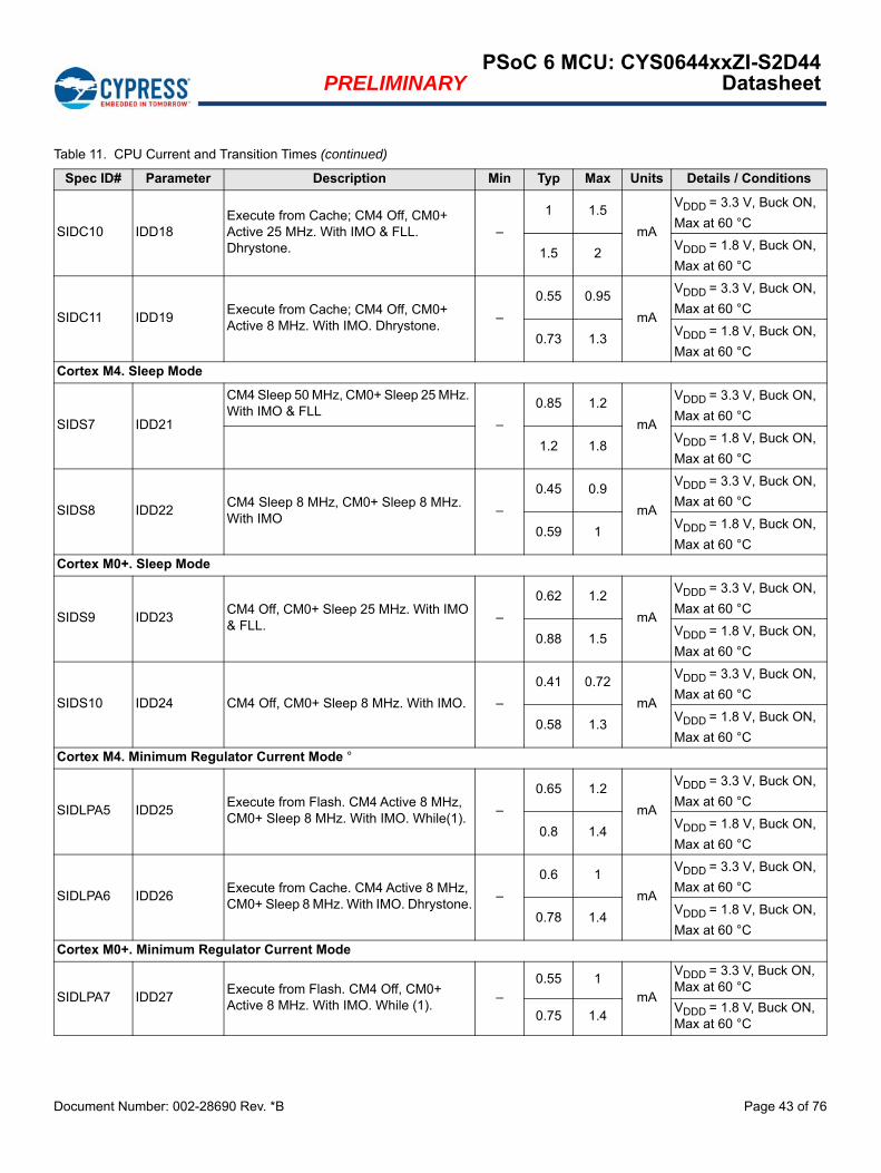
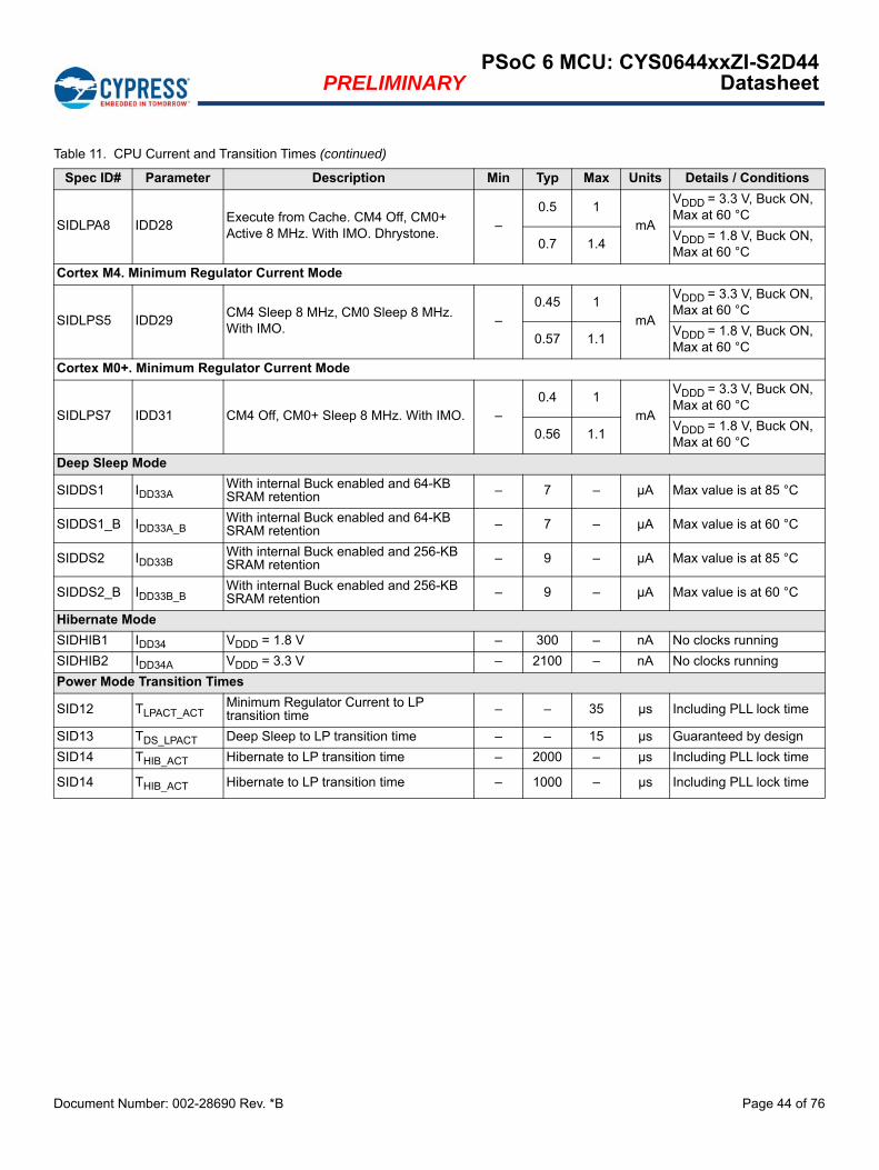
Table 11. CPU Current and Transition Times
Spec ID# Parameter Description Min Typ Max Units Details / Conditions
LP RANGE POWER SPECIFICATIONS (for VCCD = 1.1 V with Buck and LDO)
Cortex-M4. Active Mode
Execute with Cache Disabled (Flash)
SIDF1 IDD1Execute from Flash; CM4 Active 50 MHz, CM0+ Sleep 25 MHz. With IMO & FLL. While(1).
–
2.85 4.5
mA
VDDD = 3.3 V, Buck ON, Max at 60 °C
4.1 5.1VDDD = 1.8 V, Buck ON, Max at 60 °C
6.8 10VDDD = 1.8 to 3.3 V, LDO, max at 60 °C
SIDF2 IDD2Execute from Flash; CM4 Active 8 MHz, CM0+ Sleep 8 MHz.With IMO. While(1)
SID308 VCSD Voltage range of operation 1.7 – 3.6 V 1.71–3.6 V
SID308A VCOMPIDAC Voltage compliance range of IDAC 0.6 –VDDA –
0.6 V VDDA – VREF ≥ 0.6 V
SID309 IDAC1DNL DNL –1 – 1 LSB –
SID310 IDAC1INL INL –3 – 3 LSBIf VDDA < 2 V then for LSB of 2.4 µA or less
SID311 IDAC2DNL DNL –1 – 1 LSB –
SID312 IDAC2INL INL –3 – 3 LSBIf VDDA < 2 V then for LSB of 2.4 µA or less
SNRC of the following is Ratio of counts of finger to noise. Measured typical devices at room temperature using Dual IDAC + PRS Clock Mode. Best performance is when using the PASS reference and the PLL.
SID313_1A SNRC_1SRSS Reference. IMO + FLL Clock Source. 0.1-pF sensitivity.
5 – – Ratio 9.5-pF max. capacitance
SID313_1B SNRC_2SRSS Reference. IMO + FLL Clock Source. 0.3-pF sensitivity.
5 – – Ratio 31-pF max. capacitance
SID313_1C SNRC_3SRSS Reference. IMO + FLL Clock Source. 0.6-pF sensitivity.
5 – – Ratio 61-pF max. capacitance
SID313_2A SNRC_4PASS Reference. IMO + FLL Clock Source. 0.1-pF sensitivity.
5 – – Ratio 12-pF max. capacitance
SID313_2B SNRC_5PASS Reference. IMO + FLL Clock Source. 0.3-pF sensitivity.
5 – – Ratio 47-pF max. capacitance
SID313_2C SNRC_6PASS Reference. IMO + FLL Clock Source. 0.6-pF sensitivity.
5 – – Ratio 86-pF max. capacitance
SID313_3A SNRC_7PASS Reference. IMO + PLL Clock Source. 0.1-pF sensitivity.
5 – – Ratio 25-pF max. capacitance
SID313_3B SNRC_8PASS Reference. IMO + PLL Clock Source. 0.3-pF sensitivity.
5 – – Ratio 86-pF max. capacitance
SID313_3C SNRC_9PASS Reference. IMO + PLL Clock Source. 0.6-pF sensitivity.
5 – – Ratio 168-pF Max. capacitance
Document Number: 002-28690 Rev. *B Page 50 of 76
PRELIMINARYPSoC 6 MCU: CYS0644xxZI-S2D44
Datasheet
SID314 IDAC1CRT1Output current of IDAC1 (7 bits) in low range
4.2 – 5.7 µA LSB = 37.5-nA typ.
SID314A IDAC1CRT2Output current of IDAC1 (7 bits) in medium range
33.7 – 45.6 µA LSB = 300-nA typ.
SID314B IDAC1CRT3Output current of IDAC1 (7 bits) in high range
270 – 365 µA LSB = 2.4-µA typ.
SID314C IDAC1CRT12Output current of IDAC1 (7 bits) in low range, 2X mode
8 – 11.4 µALSB = 37.5-nA typ. 2X output stage
SID314D IDAC1CRT22Output current of IDAC1 (7 bits) in medium range, 2X mode
67 – 91 µALSB = 300-nA typ. 2X output stage
SID314E IDAC1CRT32Output current of IDAC1 (7 bits) in high range, 2X mode. VDDA > 2 V
540 – 730 µALSB = 2.4-µA typ. 2X output stage
SID315 IDAC2CRT1Output current of IDAC2 (7 bits) in low range
4.2 – 5.7 µA LSB = 37.5-nA typ.
SID315A IDAC2CRT2Output current of IDAC2 (7 bits) in medium range
33.7 – 45.6 µA LSB = 300-nA typ.
SID315B IDAC2CRT3Output current of IDAC2 (7 bits) in high range
270 – 365 µA LSB = 2.4-µA typ.
SID315C IDAC2CRT12Output current of IDAC2 (7 bits) in low range, 2X mode
8 – 11.4 µALSB = 37.5-nA typ. 2X output stage
SID315D IDAC2CRT22Output current of IDAC2 (7 bits) in medium range, 2X mode
67 – 91 µALSB = 300-nA typ. 2X output stage
SID315E IDAC2CRT32Output current of IDAC2 (7 bits) in high range, 2X mode. VDDA > 2V
540 – 730 µALSB = 2.4-µA typ. 2X output stage
SID315F IDAC3CRT13Output current of IDAC in 8-bit mode in low range
8 – 11.4 µA LSB = 37.5-nA typ.
SID315G IDAC3CRT23Output current of IDAC in 8-bit mode in medium range
67 – 91 µA LSB = 300-nA typ.
SID315H IDAC3CRT33Output current of IDAC in 8-bit mode in high range. VDDA > 2V
540 – 730 µA LSB = 2.4-µA typ.
SID320 IDACOFFSET All zeroes input – – 1 LSB Polarity set by source or sink
Spec ID# Parameter Description Min Typ Max Units Details/Conditions
SID.TCPWM.1 ITCPWM1 Block current consumption at 8 MHz – – 70 µA All modes (TCPWM)
SID.TCPWM.2 ITCPWM2 Block current consumption at 24 MHz – – 180 µA All modes (TCPWM)
SID.TCPWM.2A ITCPWM3 Block current consumption at 50 MHz – – 270 µA All modes (TCPWM)
SID.TCPWM.2B ITCPWM4 Block current consumption at 100 MHz – – 540 µA All modes (TCPWM)
SID.TCPWM.3 TCPWMFREQ Operating frequency – – 100 MHz Maximum = 100 MHz
SID.TCPWM.4 TPWMENEXTInput trigger pulse width for all trigger events
2/Fc – – ns
Trigger events can be Stop, Start, Reload, Count, Capture, or Kill depending on which mode of operation is selected. Fc is counter operating frequency.
Spec ID Parameter Description Min Typ Max Units Details/Conditions
SID159 FLCD LCD frame rate 10 50 150 Hz –
Document Number: 002-28690 Rev. *B Page 56 of 76
PRELIMINARYPSoC 6 MCU: CYS0644xxZI-S2D44
Datasheet
Memory
Table 25. Flash Specifications[4]
Spec ID Parameter Description Min Typ Max Units Details/Conditions
Flash DC Specifications
SID173A IPE Erase and program current – – 6 mA –
Flash AC Specifications
SID174 TROWWRITE Row write time (erase and program) – – 16 ms Row = 512 bytes
SID175 TROWERASE Row erase time – – 11 ms –
SID176 TROWPROGRAM Row program time after erase – – 5 ms –
SID178 TBULKERASE Bulk erase time (2048 KB) – – 11 ms –
SID179 TSECTORERASE Sector erase time (256 KB) – – 11 ms 512 rows per sector
SID178S TSSERIAE Subsector erase time – – 11 ms 8 rows per subsector
SID179S TSSWRITESubsector write time; 1 erase plus 8 program times
– – 51 ms –
SID180S TSWRITESector write time; 1 erase plus 512 program times
– – 2.6 seconds –
SID180 TDEVPROG Total device write time – – 30 seconds –
SID181 FEND Flash endurance 100K – – cycles –
SID182 FRET1Flash retention. TA 25 °C, 100K P/E cycles
10 – – years –
SID182A FRET2Flash retention. TA 85 °C, 10K P/E cycles
10 – – years –
SID182B FRET3Flash retention. TA 55 °C, 20K P/E cycles
20 – – years –
SID256 TWS100 Number of Wait states at 100 MHz 3 – – LP mode. VCCD = 1.1 V
SID257 TWS50 Number of Wait states at 50 MHz 2 – – ULP mode. VCCD = 0.9 V
Note4. It can take as much as 16 milliseconds to write to flash. During this time, the device should not be reset, or flash operations will be interrupted and cannot be relied
on to have completed. Reset sources include the XRES pin, software resets, CPU lockup states and privilege violations, improper power supply levels, and watchdogs. Make certain that these are not inadvertently activated.
Document Number: 002-28690 Rev. *B Page 57 of 76
PRELIMINARYPSoC 6 MCU: CYS0644xxZI-S2D44
Datasheet
System Resources
Table 26. System Resources
Spec ID Parameter Description Min Typ Max Units Details/Conditions
Power-On-Reset with Brown-out DC Specifications
Precise POR (PPOR)
SID190 VFALLPPORBOD trip voltage in Active and Sleep modes. VDDD.
1.54 – – VBOD reset guaranteed for levels below 1.54 V
SID192 VFALLDPSLP BOD trip voltage in Deep Sleep. VDDD. 1.54 – – V –
SID192A VDDRAMPMaximum power supply ramp rate (any supply)
– – 100 mV/µs Active mode
POR with Brown-out AC Specification
SID194A VDDRAMP_DSMaximum power supply ramp rate (any supply) in Deep Sleep
– – 10 mV/µs BOD operation guaranteed
Voltage Monitors DC Specifications
SID195 VHVDI1 – 1.38 1.43 1.47 V –
SID196 VHVDI2 – 1.57 1.63 1.68 V –
SID197 VHVDI3 – 1.76 1.83 1.89 V –
SID198 VHVDI4 – 1.95 2.03 2.1 V –
SID199 VHVDI5 – 2.05 2.13 2.2 V –
SID200 VHVDI6 – 2.15 2.23 2.3 V –
SID201 VHVDI7 – 2.24 2.33 2.41 V –
SID202 VHVDI8 – 2.34 2.43 2.51 V –
SID203 VHVDI9 – 2.44 2.53 2.61 V –
SID204 VHVDI10 – 2.53 2.63 2.72 V –
SID205 VHVDI11 – 2.63 2.73 2.82 V –
SID206 VHVDI12 – 2.73 2.83 2.92 V –
SID207 VHVDI13 – 2.82 2.93 3.03 V –
SID208 VHVDI14 – 2.92 3.03 3.13 V –
SID209 VHVDI15 – 3.02 3.13 3.23 V –
SID211 LVI_IDD Block current – 5 15 µA –
Voltage Monitors AC Specification
SID212 TMONTRIP Voltage monitor trip time – – 170 ns –
Document Number: 002-28690 Rev. *B Page 58 of 76
PRELIMINARYPSoC 6 MCU: CYS0644xxZI-S2D44
Datasheet
SWD Interface
Internal Main Oscillator
Internal Low-Speed Oscillator
Table 27. SWD and Trace Specifications
Spec ID# Parameter Description Min Typ Max Units Details / Conditions
SWD and Trace Interface
SID214 F_SWDCLK2 1.7 V VDDD 3.6 V – – 25 MHzLP Mode.
VCCD = 1.1 V.
SID214L F_SWDCLK2L 1.7 V VDDD 3.6 V – – 12 MHzULP Mode.
VCCD = 0.9 V.
SID215 T_SWDI_SETUP T = 1/f SWDCLK 0.25 * T – – ns –
SID216 T_SWDI_HOLD T = 1/f SWDCLK 0.25 * T – – ns –
SID217 T_SWDO_VALID T = 1/f SWDCLK – – 0.5 * T ns –
SID217A T_SWDO_HOLD T = 1/f SWDCLK 1 – – ns –
SID214T F_TRCLK_LP1With Trace Data setup/hold times of 2/1 ns respectively
– – 50 MHz LP Mode. VDD = 1.1 V.
SID215T F_TRCLK_LP2With Trace Data setup/hold times of 3/2 ns respectively
– – 50 MHz LP Mode. VDD = 1.1 V.
SID216T F_TRCLK_ULPWith Trace Data setup/hold times of 3/2 ns respectively
– – 20 MHz ULP Mode. VDD = 0.9 V.
Table 28. IMO DC Specifications
Spec ID Parameter Description Min Typ Max Units Details/Conditions
SID218 IIMO1 IMO operating current at 8 MHz – 9 15 µA –
Table 29. IMO AC Specifications
Spec ID Parameter Description Min Typ Max Units Details/Conditions
SID223 FIMOTOL1Frequency variation centered on 8 MHz
– – ±2 % –
SID227 TJITR Cycle-to-cycle and period jitter – 250 – ps –
Table 30. ILO DC Specification
Spec ID Parameter Description Min Typ Max Units Details/Conditions
SID231 IILO2 ILO operating current at 32 kHz – 0.3 0.7 µA –
Table 31. ILO AC Specifications
Spec ID Parameter Description Min Typ Max Units Details/Conditions
SID234 TSTARTILO1 ILO startup time – – 7 µsStartup time to 95% of final frequency
SID236 TLIODUTY ILO duty cycle 45 50 55 % –
SID237 FILOTRIM1 32-kHz trimmed frequency 28.8 32 36.1 kHz
Document Number: 002-28690 Rev. *B Page 59 of 76
PRELIMINARYPSoC 6 MCU: CYS0644xxZI-S2D44
Datasheet
Crystal Oscillator Specifications
External Clock Specifications
PLL Specifications
Table 32. ECO Specifications
Spec ID Parameter Description Min Typ Max Units Details/Conditions
MHz ECO DC Specifications
SID316 IDD_MHzBlock operating current with Cload up to 18 pF
– 800 1600 µAMax = 33 MHz,
Type = 16 MHz
MHz ECO AC Specifications
SID317 F_MHz Crystal frequency range 16 – 35 MHzSome restrictions apply. Refer to the device TRM.
kHz ECO DC Specifications
SID318 IDD_kHz Block operating current with 32-kHz crystal – 0.38 1 µA –
SID321E ESR32K Equivalent series resistance – 80 – kΩ –
Table 41. SD Host Controller and eMMC Specifications
Spec ID# Parameter Description Min Typ Max Units Details / Conditions
SD Host Controller and eMMC Specifications (Block Clock must be divided by 2 or more when used as source in DDR modes. Specifications are Guaranteed by Design.
SID_SD390 SD_DS I/O drive select 4 – 4 mA drive_sel = '01' for all modes
SID_SD391 SD_TR Input transition time 0.7 – 3 ns –
GPIO general-purpose input/output, applies to a PSoC pin
HMAC Hash-based message authentication code
HSIOM high-speed I/O matrix
I/O input/output, see also GPIO, DIO, SIO, USBIO
I2C, or IIC Inter-Integrated Circuit, a communications protocol
I2S inter-IC sound
IC integrated circuit
IDAC current DAC, see also DAC, VDAC
IDE integrated development environment
ILO internal low-speed oscillator, see also IMO
IMO internal main oscillator, see also ILO
INL integral nonlinearity, see also DNL
IOSS input output subsystem
IoT internet of things
IPC inter-processor communication
IRQ interrupt request
ISR interrupt service routine
ITM instrumentation trace macrocell
JTAG Joint Test Action Group
LCD liquid crystal display
LINLocal Interconnect Network, a communications protocol
LP low power
LS low-speed
LUT lookup table
LVD low-voltage detect, see also LVI
LVI low-voltage interrupt
LVTTL low-voltage transistor-transistor logic
MAC multiply-accumulate
MCU microcontroller unit
MCWDT multi-counter watchdog timer
MISO master-in slave-out
MMIO memory-mapped input output
MOSI master-out slave-in
MPU memory protection unit
MSL moisture sensitivity level
Msps million samples per second
MTB micro trace buffer
Acronym Description
Document Number: 002-28690 Rev. *B Page 72 of 76
PRELIMINARYPSoC 6 MCU: CYS0644xxZI-S2D44
Datasheet
MUL multiplier
NC no connect
NMI nonmaskable interrupt
NVIC nested vectored interrupt controller
NVL nonvolatile latch, see also WOL
OTP one-time programmable
OVP over voltage protection
OVT overvoltage tolerant
PASS programmable analog subsystem
PCB printed circuit board
PCM pulse code modulation
PDM pulse density modulation
PHY physical layer
PICU port interrupt control unit
PLL phase-locked loop
PMIC power management integrated circuit
POR power-on reset
PPU peripheral protection unit
PRNG pseudo random number generator
PSoC® Programmable System-on-Chip™
PSRR power supply rejection ratio
PWM pulse-width modulator
QD quadrature decoder
QSPI quad serial peripheral interface
RAM random-access memory
RISC reduced-instruction-set computing
RMS root-mean-square
ROM read-only memory
RSARivest–Shamir–Adleman, a public-key cryptography algorithm
RTC real-time clock
RWW read-while-write
RX receive
S/H sample and hold
SAR successive approximation register
SARMUX SAR ADC multiplexer bus
SC/CT switched capacitor/continuous time
SCB serial communication block
SCL I2C serial clock
SD Secure Digital
SDA I2C serial data
SDHC Secure Digital host controller
SDR single data rate
Sflash supervisory flash
SHA secure hash algorithm
SINAD signal to noise and distortion ratio
SMPU shared memory protection unit
Acronym Description
SNR signal-to-noise ration
SOF start of frame
SONOSsilicon-oxide-nitride-oxide-silicon, a flash memory technology
SPISerial Peripheral Interface, a communications protocol
SRAM static random access memory
SROM supervisory read-only memory
SRSS system resources subsystem
SWD serial wire debug, a test protocol
SWJ serial wire JTAG
SWO single wire output
SWV single-wire viewer
TCPWM timer, counter, pulse-width modulator
TDM time division multiplexed
THD total harmonic distortion
TQFP thin quad flat package
TRM technical reference manual
TRNG true random number generator
TX transmit
UARTUniversal Asynchronous Transmitter Receiver, a communications protocol
UDB universal digital block
ULP ultra-low power
USB Universal Serial Bus
WCO watch crystal oscillator
WDT watchdog timer
WIC wakeup interrupt controller
WLCSP wafer level chip scale package
XIP execute-in-place
XRES external reset input pin
Acronym Description
Document Number: 002-28690 Rev. *B Page 73 of 76
PRELIMINARYPSoC 6 MCU: CYS0644xxZI-S2D44
Datasheet
Document Conventions
Units of Measure
Table 48. Units of Measure
Symbol Unit of Measure
°C degrees Celsius
dB decibel
fF femto farad
Hz hertz
KB 1024 bytes
kbps kilobits per second
khr kilohour
kHz kilohertz
k kilo ohm
ksps kilosamples per second
LSB least significant bit
Mbps megabits per second
MHz megahertz
M mega-ohm
Msps megasamples per second
µA microampere
µF microfarad
µH microhenry
µs microsecond
µV microvolt
µW microwatt
mA milliampere
ms millisecond
mV millivolt
nA nanoampere
ns nanosecond
nV nanovolt
W ohm
pF picofarad
ppm parts per million
ps picosecond
s second
sps samples per second
sqrtHz square root of hertz
V volt
Table 48. Units of Measure (continued)
Symbol Unit of Measure
Document Number: 002-28690 Rev. *B Page 74 of 76
PRELIMINARYPSoC 6 MCU: CYS0644xxZI-S2D44
Datasheet
Errata
This section describes the errata for the CYS0644xxZI-S2D44 product line. Details include errata trigger conditions, scope of impact,available workarounds, and silicon revision applicability. Compare this document to the device's datasheet for a complete functionaldescription.
Contact your local Cypress Sales Representative if you have questions.
Part Numbers Affected
Qualification Status
Engineering Samples
Errata Summary
This table defines the errata applicability to available PSoC 6 CYS0644xxZI-S2D44 devices.
Part Number Device Characteristics
CYS0644xxZI-S2D44 CYS0644xxZI-S2D44 Product Line
Items PSoCCYS0644xxZI-S2D44 Silicon Revision Fix Status
[1] MHz ECO usage requires Ports 11, 12, and 13 be restricted to slow slew rate (2.5-MHz max frequency).
All Production silicon Resolution planned by Q3 '20
1. MHz ECO usage requires Ports 11, 12, and 13 be restricted to slow slew rate (2.5-MHz max frequency).
Problem DefinitionMHz ECO is sensitive to GPIO switching noise on adjacent I/O ports and requires edge rates be restricted when the MHz ECO is used
Parameters AffectedSlew rate is restricted to slow switching and this affects switching frequency which is restricted to 2.5 MHz
Trigger Condition(s) Usage of fast slew rates on ECO Port and adjacent ports (Ports 11, 12, and 13).
Scope of ImpactSlew rates must be restricted to slow mode for reliable ECO operation. Note this includes the QSPI interface port (Port 11).
Workaround None
Fix Status Investigation underway. Resolution planned by Q3 20.
Revision ECN Submission Date Description of Change
** 6710233 01/13/2020 New datasheet
*A 6854009 04/16/2020
Updated Features.Updated Functional Description.Updated SAR ADC 1 Msps references to 2 Msps.Removed reference to e.MMC DDR modeUpdated Pinouts.Updated Electrical Specifications.Edited SAR Specs to split VDDA dependent specs into separate specs instead of having qualifying comments. Also moved Supply Range specs from Description column to Details/Conditions column. Added SAR ADC 2 Msps supply current specs. Updated SAR ADC input impedance RC values to support 9RC 2 Msps sampling.Updated PSoC 6 MPN Decoder.
*B 6891487 06/11/2020Updated Development Ecosystem, GPIO, and LCD sections.Added External Crystal Oscillators.
Document Number: 002-28690 Rev. *B Revised June 12, 2020 Page 76 of 76
TO THE EXTENT PERMITTED BY APPLICABLE LAW, CYPRESS MAKES NO WARRANTY OF ANY KIND, EXPRESS OR IMPLIED, WITH REGARD TO THIS DOCUMENT OR ANY SOFTWAREOR ACCOMPANYING HARDWARE, INCLUDING, BUT NOT LIMITED TO, THE IMPLIED WARRANTIES OF MERCHANTABILITY AND FITNESS FOR A PARTICULAR PURPOSE. No computingdevice can be absolutely secure. Therefore, despite security measures implemented in Cypress hardware or software products, Cypress does not assume any liability arising out of any security breach,such as unauthorized access to or use of a Cypress product. In addition, the products described in these materials may contain design defects or errors known as errata which may cause the productto deviate from published specifications. To the extent permitted by applicable law, Cypress reserves the right to make changes to this document without further notice. Cypress does not assume anyliability arising out of the application or use of any product or circuit described in this document. Any information provided in this document, including any sample design information or programmingcode, is provided only for reference purposes. It is the responsibility of the user of this document to properly design, program, and test the functionality and safety of any application made of thisinformation and any resulting product. Cypress products are not designed, intended, or authorized for use as critical components in systems designed or intended for the operation of weapons, weaponssystems, nuclear installations, life-support devices or systems, other medical devices or systems (including resuscitation equipment and surgical implants), pollution control or hazardous substancesmanagement, or other uses where the failure of the device or system could cause personal injury, death, or property damage ("Unintended Uses"). A critical component is any component of a deviceor system whose failure to perform can be reasonably expected to cause the failure of the device or system, or to affect its safety or effectiveness. Cypress is not liable, in whole or in part, and youshall and hereby do release Cypress from any claim, damage, or other liability arising from or related to all Unintended Uses of Cypress products. You shall indemnify and hold Cypress harmless fromand against all claims, costs, damages, and other liabilities, including claims for personal injury or death, arising from or related to any Unintended Uses of Cypress products.
Cypress, the Cypress logo, Spansion, the Spansion logo, and combinations thereof, WICED, PSoC, CapSense, EZ-USB, F-RAM, and Traveo are trademarks or registered trademarks of Cypress inthe United States and other countries. For a more complete list of Cypress trademarks, visit cypress.com. Other names and brands may be claimed as property of their respective owners.
Sales, Solutions, and Legal Information
Worldwide Sales and Design Support
Cypress maintains a worldwide network of offices, solution centers, manufacturer’s representatives, and distributors. To find the officeclosest to you, visit us at Cypress Locations.
Products
Arm® Cortex® Microcontrollers cypress.com/arm
Automotive cypress.com/automotive
Clocks & Buffers cypress.com/clocks
Interface cypress.com/interface
Internet of Things cypress.com/iot
Memory cypress.com/memory
Microcontrollers cypress.com/mcu
PSoC cypress.com/psoc
Power Management ICs cypress.com/pmic
Touch Sensing cypress.com/touch
USB Controllers cypress.com/usb
Wireless Connectivity cypress.com/wireless
PSoC® Solutions
PSoC 1 | PSoC 3 | PSoC 4 | PSoC 5LP | PSoC 6 MCU
Cypress Developer Community
Community | Code Examples | Projects | Video | Blogs | Training| Components