1 FP7-ICT-2009-4/248454 QoSMOS D4.4 QoSMOS Transceiver – Design and Performance Contractual Date of Delivery to the CEC: 31-Dec-2012 Actual Date of Delivery to the CEC: 31-Dec-2012 Editor(s): Vincent Berg (CEA) Author(s): Mario Schühler, Mengistu Tessema (Fraunofer IIS), Jean-Baptiste Doré, Xavier Popon, Ignacio Vergara, Dominique Noguet, Vincent Berg (CEA) Reviewer(s): David Depierre (TCF) Workpackage: WP4 Est. person months: 32.5PM Security: PU Nature: R Version: 1.0 Total number of pages: 65 Abstract: TV white space (TVWS) has been considered one of the very first portions of the spectrum where the concept of cognitive radio (CR) meets regulatory and actual deployment-driven requirement figures. Dynamic Spectrum Access in TVWS is likely to result in a heavily fragmented spectrum. This has required the development of a flexible RF transceiver. Furthermore, the requirement to meet the current adjacent channel leakage regulations has motivated the use of alternative multicarrier modulation schemes exhibiting well-controlled power leakage outside the useful bandwidth. The design and implementation of a Filter Bank Multicarrier Transceiver has been considered for the QoSMOS proof-of-concept prototypes. Implementation of the proposed approach is detailed. Keyword list: Cognitive Radio, Scenario, Transceiver architecture, Flexible design, Physical layer, Agile RF Transceiver, Multicarrier modulation, TVWS Quality Of Service and MObility driven cognitive radio Systems
Transcript
1
FP7-ICT-2009-4/248454
QoSMOS
D4.4
QoSMOS Transceiver – Design and Performance
Contractual Date of Delivery to the CEC: 31-Dec-2012
Actual Date of Delivery to the CEC: 31-Dec-2012
Editor(s): Vincent Berg (CEA)
Author(s): Mario Schühler, Mengistu Tessema (Fraunofer IIS), Jean-Baptiste Doré,
Xavier Popon, Ignacio Vergara, Dominique Noguet, Vincent Berg (CEA)
Reviewer(s): David Depierre (TCF)
Workpackage: WP4
Est. person months: 32.5PM
Security: PU
Nature: R
Version: 1.0
Total number of pages: 65
Abstract:
TV white space (TVWS) has been considered one of the very first portions of the spectrum where the
concept of cognitive radio (CR) meets regulatory and actual deployment-driven requirement figures.
Dynamic Spectrum Access in TVWS is likely to result in a heavily fragmented spectrum. This has
required the development of a flexible RF transceiver. Furthermore, the requirement to meet the
current adjacent channel leakage regulations has motivated the use of alternative multicarrier
modulation schemes exhibiting well-controlled power leakage outside the useful bandwidth. The
design and implementation of a Filter Bank Multicarrier Transceiver has been considered for the
QoSMOS proof-of-concept prototypes. Implementation of the proposed approach is detailed.
3 A FLEXIBLE TRANSCEIVER ................................................................................................. 11
3.1 THE NEED FOR A FLEXIBLE TRANSCEIVER ............................................................................. 11 3.2 FLEXIBLE TRANSCEIVER SPECIFICATIONS ............................................................................ 14
3.2.1 Requirements imposed by regulation ............................................................................ 15 3.2.2 Derived requirements and FBMC properties ................................................................ 16 3.2.3 Specification summary for QosMOS flexible transceiver .............................................. 19
4 HARDWARE ARCHITECTURE OF QOSMOS FLEXIBLE TRANSCEIVER ................. 20
An increasing number of European and world-wide regulatory bodies and authorities allow
unlicensed, opportunistic use of certain parts of the spectrum, freed by the Digital Switch Over (DSO)
in the TV broadcast bands under relaxed regulatory and administrative requirements. Therefore, TV
white space (TVWS) has been considered one of the very first portions of the spectrum where the
concepts of Cognitive Radio (CR) meet regulatory and actual deployment-driven requirement figures.
In order to avoid possible harmful interference with incumbent TV broadcasting systems and wireless
microphones, these opportunistic devices need to comply with certain limitations. These include their
effective radiated power and adjacent-channel leakage requirements. Current regulations specify
relatively strict requirements which pose challenges on the implementation using conventional
modulation schemes and signal processing techniques.
As stipulated in the P1900.7 contribution [BER11], the LTE downlink waveform requires additional
filtering to meet the -55 dB ACLR requirement which in turn leads to significant complexity increase
in the implementation. Furthermore, Dynamic Spectrum Access (DSA) in TVWS is likely to result in
heavily fragmented spectrum. Filter Bank Multicarrier Modulation (FBMC) has been considered well
suited and a first implementation geared towards these applications is proposed in this document.
Section 3 recalls the specificities of TVWS and derives the requirements for a flexible transceiver in
this context. These requirements served as a basis for the development of the flexible transceiver.
Section 4 presents the architecture of the implemented FBMC flexible transceiver. RF hardware and
baseband architectures are detailed with a particular emphasis on the trade-off made for flexible
cognitive radio usage.
Section 5 gives performance results of the transceiver. Particularly, ACLR requirements are validated
in both contexts: single frequency transmission and spectrum pooling. Preliminary results of the
receiver are also given.
Finally, section 6 gives the conclusions that can be drawn from this work, the chapter also points the
way ahead to further work that should be undertaken to complement the reported findings.
11
3 A Flexible Transceiver
3.1 The need for a flexible transceiver
CR was first introduced by Mitola [Mit00] as a radio system that can adapt its parameters based upon
changes in its context environment. Whatever the origin and the nature of these changes, and the
purpose of the decision strategy, the ability to adapt to changes is essential to the concept. Therefore,
CR has capitalized on the flexible radio concept in a broad sense, or according to Mitola on the
software radio concept he introduced in [MIT95].
More recent work has focussed on opportunistic radio, where contextual environment is limited to the
knowledge of spectrum usage [ORAD3.3]. The architectural work introduced in Oracle focussed on a
multi-band transceiver, where each band was addressed individually by a specific BAW filter to
guarantee low adjacent leakage at the transmitter. Although the concept enabled some flexibility at the
modulator stage, the bands of interest were predetermined by the Bulk Acoustic Wave (BAW) filters
for which tunability is limited. Other experimental setups were limited to Industrial, Scientific and
Medical band (ISM) radiofrequency bands in order to restrict the requirements on the RF stages
[RAY05, MIS05, BIA09]. These setups enabled to test algorithms in an unlicensed environment, but
their impact on actual deployment was limited due to the competition of well-established
communication systems in these bands. Therefore these setups did not demonstrate all the potential of
cognitive radio.
In some countries, the DSO in TV bands has recently resulted in relaxed regulatory regimes, where
unlicensed spectrum use is allowed, provided that non-harmful interference to incumbent systems is
guaranteed. This move was first initiated in the USA, where the first proposed rules for the
“Unlicensed Operation in the TV Broadcast Bands” were published as early as 2004 [FCC04] and
finalized in 2009 [FCC09]. A same initiative followed in the UK [OFC09]. A similar trend is currently
taking place in other European countries [CEPT09] and in Australia [FRE11]. Consequently, the
unused TV spectrum, referred to as TVWS, has become one of the very first portions of the spectrum
where the concepts of CR meet regulatory and actual deployment-driven requirement figures. In the
meantime, standardization efforts pushed by the IEEE 802 groups [802.22, 802.11af], has given DSA
for wireless users an opportunity for practical deployment in the TVWS. The recently established
working group IEEE P1900.7 on White Space Radio has given even more momentum to this trend and
is perceived as a real opportunity for future DSA and flexible radio developments.
In [OFC09] it was made clear that opportunities for TVWS DSA exist, but that available channels
depend on location and time (Figure 3-1).
12
Figure 3-1: TVWS available spectrum according to [OFC09]
[NEK10] analysed the distribution of these channels across the TVWS spectrum (Figure 3-2). It can be
concluded from this study that an efficient exploitation of the spectrum asset depends on the ability of
the TVWS radio to exploit fragmented spectrum.
Figure 3-2: Example of spectrum availability in London [NEK10]
From these conclusions, and in order to address the scenarios considered in QoSMOS [LEH12], a set
of requirements have been derived for a CR hardware platform. In order to exercise the mobility
scenarios, the platform should be contained in size (i.e.: it should be possible to hold the demonstrator
with one hand) and battery powered. Some of the studied advanced modulations and sensing
algorithms will be evaluated in real time. The radio link and the other stages of the cognitive radio,
such as the reconfiguration of the radio should also be available on the platform. An application will
be run on top of the radio link to demonstrate Quality of Service (QoS) capability through advanced
Medium Access Control (MAC) features.
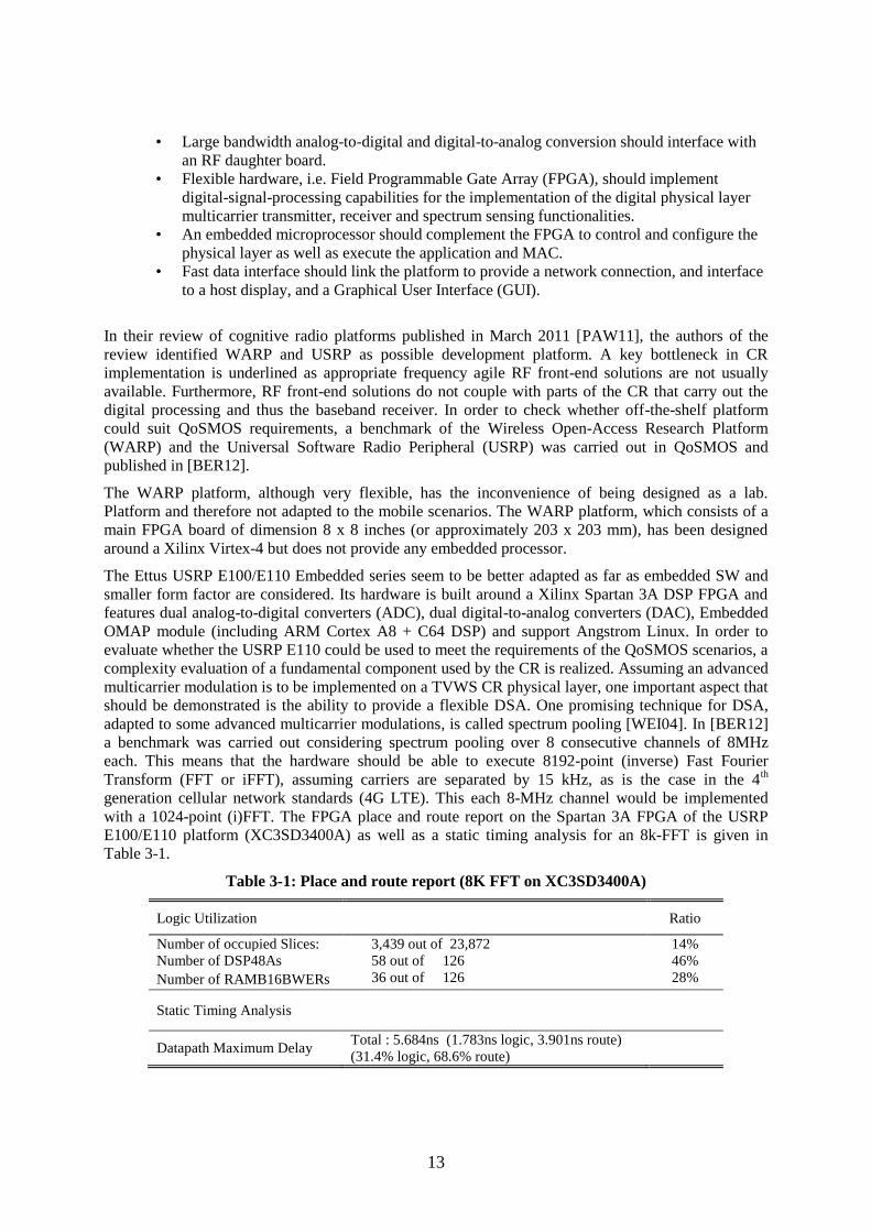
The CR hardware platform should include the following functionalities:
13
• Large bandwidth analog-to-digital and digital-to-analog conversion should interface with
an RF daughter board. • Flexible hardware, i.e. Field Programmable Gate Array (FPGA), should implement
digital-signal-processing capabilities for the implementation of the digital physical layer
multicarrier transmitter, receiver and spectrum sensing functionalities. • An embedded microprocessor should complement the FPGA to control and configure the
physical layer as well as execute the application and MAC. • Fast data interface should link the platform to provide a network connection, and interface
to a host display, and a Graphical User Interface (GUI).
In their review of cognitive radio platforms published in March 2011 [PAW11], the authors of the
review identified WARP and USRP as possible development platform. A key bottleneck in CR
implementation is underlined as appropriate frequency agile RF front-end solutions are not usually
available. Furthermore, RF front-end solutions do not couple with parts of the CR that carry out the
digital processing and thus the baseband receiver. In order to check whether off-the-shelf platform
could suit QoSMOS requirements, a benchmark of the Wireless Open-Access Research Platform
(WARP) and the Universal Software Radio Peripheral (USRP) was carried out in QoSMOS and
published in [BER12].
The WARP platform, although very flexible, has the inconvenience of being designed as a lab.
Platform and therefore not adapted to the mobile scenarios. The WARP platform, which consists of a
main FPGA board of dimension 8 x 8 inches (or approximately 203 x 203 mm), has been designed
around a Xilinx Virtex-4 but does not provide any embedded processor.
The Ettus USRP E100/E110 Embedded series seem to be better adapted as far as embedded SW and
smaller form factor are considered. Its hardware is built around a Xilinx Spartan 3A DSP FPGA and
features dual analog-to-digital converters (ADC), dual digital-to-analog converters (DAC), Embedded
OMAP module (including ARM Cortex A8 + C64 DSP) and support Angstrom Linux. In order to
evaluate whether the USRP E110 could be used to meet the requirements of the QoSMOS scenarios, a
complexity evaluation of a fundamental component used by the CR is realized. Assuming an advanced
multicarrier modulation is to be implemented on a TVWS CR physical layer, one important aspect that
should be demonstrated is the ability to provide a flexible DSA. One promising technique for DSA,
adapted to some advanced multicarrier modulations, is called spectrum pooling [WEI04]. In [BER12]
a benchmark was carried out considering spectrum pooling over 8 consecutive channels of 8MHz
each. This means that the hardware should be able to execute 8192-point (inverse) Fast Fourier
Transform (FFT or iFFT), assuming carriers are separated by 15 kHz, as is the case in the 4th
generation cellular network standards (4G LTE). This each 8-MHz channel would be implemented
with a 1024-point (i)FFT. The FPGA place and route report on the Spartan 3A FPGA of the USRP
E100/E110 platform (XC3SD3400A) as well as a static timing analysis for an 8k-FFT is given in
Table 3-1.
Table 3-1: Place and route report (8K FFT on XC3SD3400A)
Logic Utilization Ratio
Number of occupied Slices: 3,439 out of 23,872 14%
Number of DSP48As 58 out of 126 46%
Number of RAMB16BWERs 36 out of 126 28%
Static Timing Analysis
Datapath Maximum Delay Total : 5.684ns (1.783ns logic, 3.901ns route)
(31.4% logic, 68.6% route)
14
The results show that although the Spartan 3A DSP meets the requirement for one 8k FFT, significant
amount of DSP resources have been used by the operation. Considering that at least two FFT of the
evaluated size may be required (one for the transmit data path and one for receive data path), and that
timing constraints may not be met if the DSP resources are replaced by standard logic cells (Slices), it
was concluded that the Spartan 3A DSP was too resource limited for the implementation of a flexible
multi-carrier air interface application. It was therefore concluded that a specific hardware platform was
needed for the implementation of the QoSMOS radio.
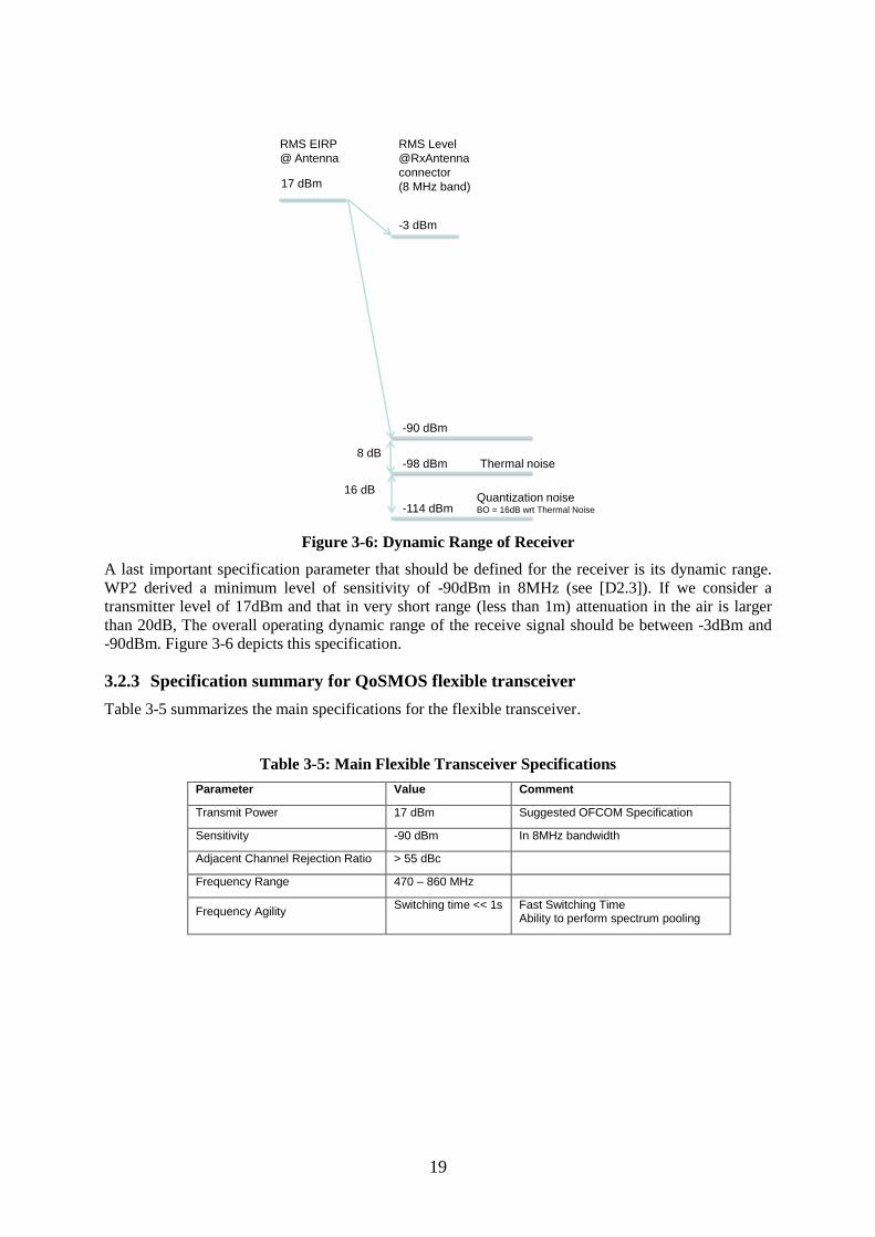
3.2 Flexible Transceiver Specifications
The QoSMOS project developed therefore the hardware platform presented in Figure 3-3. The
components that are the main elements of this platform have been described in details in [D7.2] and
[D7.3].
Figure 3-3: General Architecture of QoSMOS Hardware platform
The architecture of the hardware platform proposed a software radio approach for the implementation
of the flexible transceiver. A flexible RF board is connected to the baseband through high speed
analog-to-digital converters and high speed digital-to-analog converters. Dedicated flexible RF boards
have been developed. Special care has been put in the design to meet the required TVWS
specifications. RF boards are separated into transmit and receive boards and allow flexible RF
operation of the carrier frequency and output power over the Ultra High Frequency (UHF) band from
470 MHz up to 860 MHz. Performance with regard to adjacent channel rejection ratio has been
considered as well as transmitter power in the TVWS.
Many countries have considered cognitive access to the TVWS but only the US and the UK have so
far proposed parameter figures. These first elements of specifications for the CR in the TVWS have
already been described in previous deliverables and notably in [D1.3] and [D2.3]. They are however
recalled here as they serve as a basis for the specification of the flexible transceiver developed during
the project.
JTAGXilinx
JTAGARM
TexasDM3730
XilinxXC7K325T
FlashPROM Xilinx
XCF128XBufferRS232
Quad DACAD9148
2 dual ADCAD9643
Rx I/Q
Tx I/Q
USBLink OTG
PC
PHY MACLAN9220
RFBoard
Ethernet
10/100 Mbits/sHigh-speed USB
480 Mbds
15
3.2.1 Requirements imposed by regulation
The maximum allowed transmit power of the opportunistic systems is a particularly important
parameter as it is limited to levels that ensure non-interference to DTT systems that are in the same
channel band (co-channel interference) or adjacent to the band (adjacent channel interference). The
FCC considers two types of devices. Fixed devices (FD) are allowed to operate at up to 30dBm (1W)
transmit power and with a gain antenna to achieve 36dBm (4W) EIRP. Personal/portable devices
(PPD) are allowed to operate at up to 20dBm (100mW) EIRP in non-adjacent channels. This limit is
reduced to 16dBm (40mW) EIRP when operating on a channel adjacent to a TV occupied channel. In
both cases, antenna gain is not allowed. The FCC also modifies the power requirements of PPDs
according to the way primary systems are detected. The FCC suggests that PPDs should either have
geolocation capabilities or be under the control of an FD. The FCC allows PPD that do not operate
under these conditions but rather have spectrum sensing capabilities to detect TV stations. However,
transmit power is limited to 17dBm (50mW) EIRP for these devices. Further than transmit powers, the
FCC states that out-of-band emissions should be limited to 55dB below the power level in the band
they occupy, as measured in a band of 100kHz. It should be noted that FDs are not allowed to operate
in adjacent channels, which means that the maximal interference level should be calculated
considering the 4mW condition, leading to levels similar to the one of the OFCOM (-47dBm for a
6MHz channel). OFCOM considered another approach and concluded that opportunistic system
maximal power level has to be set to 4dBm (2.5mW) EIRP in channels adjacent to DTT services.
However, in non-adjacent channels, filters have much better rejection capabilities, and 17dBm
(50mW) EIRP can be allowed in these channels. Out-of-band radiation should be kept below -46dBm.
Table 3-2: FCC and OFCOM TVWS transmit parameters
Parameter FCC OFCOM Note
Power for FD in adjacent band Not allowed Not applicable
Power for FD in non-adjacent band
with geolocation capability
30dBm Not applicable FCC: 36dBm EIRP with
a gain antenna
Power for PPD in adjacent band 16dBm 4dBm Gain antenna not allowed
Power for PPD in non-adjacent band
with geo-location capability
20dBm 17dBm Gain antenna not allowed
Power for PPD in non-adjacent band
without geo-location capability
17dBm
Out-of-band performance <55dB <-46dBm Relative to in-band power
in the case of the FCC
In-service monitoring period 60s 1s
Evacuation time 2s Not specified
For these reasons, a fare assumption is to consider that out of band adjacent channel leakage rejection
should be at least 55dB below the power emitted in band for the proposed physical layer waveform.
Another important parameter is the evacuation time imposed to leave a channel occupied by an
incumbent user. The evacuation time should be less than 2 seconds everything included. Only a
fraction of that amount of time is thus allowed for the transceiver (transmitter and receiver) to
evacuate the channel and resume communications on a different one.
16
Incumbent users are expected to be of two types:
TV channels: the signal occupies an 8MHz band within the UHF Channel and is modulated
following DVB-T or DVB-T2 standards ([DVB09] and [DVB12]).
Programme Making and Special Events (PMSE), typically wireless microphones. They use
digital modulations such as Quadrature Phase Shift Keying (QPSK) or analogue modulation
such as Frequency Modulation (FM) [ETS06]. Usually the transmitted signal is of a much
shorter bandwidth than a TV channel (i.e. around 200kHz).
3.2.2 Derived requirements and FBMC properties
A set of propagation scenarios for TVWS has been defined in WP2 and has been summarized in
[D2.3]. These propagation scenarios have themselves been derived from the business scenarios
introduced in WP1 and notably documented in [D1.3].
The set of propagation scenarios is recalled here below:
1. Indoor short range for portable devices (1-100m): this corresponds to the cognitive femtocells
and ad-hoc scenarios
2. Mobile cellular (0.1 to 2km): this corresponds to the cellular extension scenario
3. Fixed long range (1-10km): this corresponds to the dynamic backhaul and rural broadband
scenarios
For each scenario, a set of propagation parameters have been derived and are summarized in [D4.2].
These are mainly maximum RMS delay spread and maximum Doppler spread for the given scenario.
By studying multiples and submultiples of 15 kHz carrier spacing and comparing carrier spacing and
coherence bandwidth it has been possible to propose a set of parameters for which flat fading
conditions are satisfied. Then, multicarrier symbol duration and coherence time have also been
compared in order to guarantee slow fading. The results of this study have been summarized in
Table 3-3.
Multicarrier modulations are mainly characterized by the following parameters: number of carriers,
carrier spacing and symbol duration. These types of modulations impose to have the carrier spacing
smaller than the coherence bandwidth and the symbol duration smaller than the coherence time: in the
frequency domain, the channel should be constant over a subcarrier while in the time domain, the
channel should be constant during the symbol interval.
17
Table 3-3: Waveform Specification derived from Scenarios
Hypothesis
Fc 630 MHz
Channel Analysis
RMS Delay
Spread
Max Speed Max Doppler
Coherence Bandwidth
Coherence Time
Indoor Short Range 0.15 us 7 km/h 4.2 Hz 1,3 kHz 100 ms
Mobile Cellular 1.50 us 144 km/h 84.0 Hz 133 kHz 5.0 ms
Fixed Long Range 2.40 us 4 km/h 2.1 Hz 83 kHz 201 ms
The interface is initialized and closed using respectively init_qosmos_fpga() and
close_qosmos_fpga() function calls. Data are sent to and received from the FPGA FIFOs using
a 16-bit data buffer and its associated function. For instance, to write to the FIFO stream 0, the
function, write_stream_0_qosmos_fpga() should be instantiated. The number of data values
stored in the table buffer, nbval, is then sent to the corresponding FIFO, stream 0.
The Configuration FIFO is connected to the configuration manager. The module allows the
configuration of the different block inside and outside the FPGA design, notably the configuration of
the baseband phase-locked loop (PLL), analog-to-digital converters (and digital-to-analog converters.
The RF parameters may also be interfaced with that module allowing dynamic configuration of the RF
modules (RF Transmitter and Receiver). The configuration parameters of the flexible transceiver are
36
also configured through this interface. The configuration interface is described in more details in
Section 4.5.
The digital core of the transmitter and the digital core of the receiver are respectively connected to
stream_in_0, stream_out_0 and stream_out_1 via two adaptation modules qos_tx and qos_acquisition.
The module qos_tx converts the data in the FIFO to data available at the input of the transmitter core
and allows for clock domain conversion: from the GPMC clock domain imposed by the ARM to the
internal clock domain used inside the digital core (i.e.: 112 MHz).
4.4.2 Baseband transceiver waveform structure
The proposed structure of the waveform implemented in the transceiver is depicted in Figure 4-21. It
is composed of a preamble of duration 4 FBMC symbols followed by data symbols. The preamble is
designed to detect accurately the start of the burst and give an accurate estimation of the channel
frequency response. It is mainly composed of carrier spaced every 4 active carriers (60 kHz) for the all
duration of the preamble. The channel is then considered static for the remaining of the duration of the
burst. For the QosMOS implementation, the channel response is not to be tracked in time for the
duration of the burst. Mobility is however guaranteed as channel response may evolve from burst-to-
burst.
Figure 4-21: Example of the proposed burst structure
4.4.3 Baseband Transceiver Core Architecture
4.4.3.1 Baseband Transmitter Core Architecture
The transmitter core architecture is composed of the following modules:
The data framing generation adapts the data to be sent to the constraints of the inner
transmitter
The inner transmitter implements the FBMC waveform generation
The digital front-end transmitter adapts the sample rate of the signal at the output of the
transmitter to the sampling rate and carrier frequency required at the DAC
37
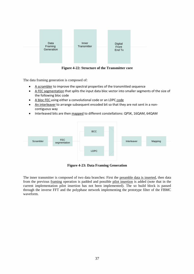
Figure 4-22: Structure of the Transmitter core
The data framing generation is composed of:
A scrambler to improve the spectral properties of the transmitted sequence
A FEC segmentation that splits the input data bloc vector into smaller segments of the size of the following bloc code
A bloc FEC using either a convolutional code or an LDPC code
An interleaver to arrange subsequent encoded bit so that they are not sent in a non-contiguous way
Interleaved bits are then mapped to different constellations: QPSK, 16QAM, 64QAM
Figure 4-23: Data Framing Generation
The inner transmitter is composed of two data branches: First the preamble data is inserted, then data
from the previous framing operation is padded and possible pilot insertion is added (note that in the
current implementation pilot insertion has not been implemented). The so build block is passed
through the inverse FFT and the polyphase network implementing the prototype filter of the FBMC
waveform.
DataFraming
Generation
Inner Transmitter
Digital Front End Tx
ScramblerFEC
segmentation
BCC
LDPC
Interleaver Mapping
38
Figure 4-24: Inner Transmitter
At the output of the inner transceiver, data is upsampled from the output of inner receiver to the
sampling frequency expected at the input of the DAC. The operation is performed in 2 stages:
First data is upsampled by a factor of 7 (from 15.36 Ms/s to 107.52 MHz),
Images are then filtered
A fractional numerically controlled oscillator (NCO) converts by cubic interpolation data to the expected sampling rate at the input of the DAC (112 MHz).
Figure 4-25: Digital Front End Tx
Special care should be taken to guarantee good ACLR performance of the generated signal. Further
description of the chosen interfaces to the DAC is described in section 4.5.
4.4.3.2 Baseband Receiver Core Architecture
The baseband core receiver is composed of the following modules:
A digital front-end RX adapts the rate of the signal sampled at the ADC to the natural rate of the data at the input to the synchronization module and the inner receiver
A Synchronization module detects the carrier frequency offset of the received signal and the start of the burst. Sampling frequency offset is considered to be negligible during the duration of the burst.
The inner receiver performs the demodulation and equalization of the synchronized signal
Demodulated data is then FEC decoded and deframed to generate the sent sequence
Figure 4-26: Receiver Overview
paddingFraming
Pilot insertion
Preambleinsertion
IFFT + PPN
upsampling Bandpass Filter Fractional NCO
Synchronization Module
Inner Receiver FEC DecoderAnd Deframing
Digital Front
End Rx
39
The receiver digital front end is composed of:
A rotor function that transforms the carrier modulated signal into I/Q baseband modulated signal and followed by a downsampling operation (by a factor 2, see section 4.5). Downsampling is preceded by a bandpass filter to avoid aliasing.
A Bandpass filter rmoves from the signal all possible aliasing
A Fractional NCO/Resampler resamples the generated signal to the appropriate sampling frequency by linear interpolation (15.36Msamples/s).
Figure 4-27: Digital Front End Rx
The receiver synchronization is estimated and applied:
The autocorrelation of the received signal allows for signal detection and carrier frequency offset (CFO) estimation
CFO is then applied to the received signal.
Figure 4-28: Receiver Synchronization
The inner receiver is at the core of the FBMC demodulator. For ease of implementation data is
demodulated using two instantiation of the FFT algorithm. A first path applies the FFT directly on the
received burst, while the other path applies the FFT on the delayed version of the received burst. Data
is then accumulated before operations of equalization and demapping. The equalizer estimates the
channel frequency response using the preamble. Since only every 4 carrier is active during the
preamble, channel estimated on the preamble is interpolated in frequency to estimate the channel on
every active carriers. Interpolation is realized using optimised Wiener filters. Then zero forcing (ZF)
equalization is applied on the data burst before demapping to generate log-likelihood ratio metrics at
the input to the FEC decoder.
Rotor I/QDownsampling
Bandpass Filter Fractional NCO
delay
Autocorrelation
CFOcorrection
40
Figure 4-29: Inner Receiver Architecture
Data is then de-interleaved, FEC decoded, blocks are then FEC de-segmented and de-scrambled.
Figure 4-30: Inner Receiver architecture
The data stream is then transfer via the OMAP GPMC interface to the ARM Cortex-A8
4.5 Transceiver Interfaces
4.5.1 RF Interface baseband TX and RX interface
As specified in section 4.2, a high IF of 280MHz has been chosen to relax the requirements of the pre-
selection filter. The choice of relatively high speed DAC and ADC for the baseband board has been
made such that conversion from intermediate frequency to inband and quadrature (or I/Q) signals is
realized in digital. This element is also a consequence of the flexible nature of the transceiver design.
Special attention is put to describe the consequences a relatively high IF would have on the baseband
design.
The QoSMOS board dispose of a quad 14-bit ADC providing a maximum sampling frequency of
250MHz and maximum bandwidth of 400MHz.
A subsampling architecture has therefore been considered, i.e. an architecture for which the sampling
frequency, fs, is smaller than the frequency of the useful signal. Subsampling on the first image has
been chosen and is given in Figure 4-31. The useful signal is around 280MHz and has a maximum
bandwidth of 40MHz. If the carrier frequency, fs, is larger than but smaller than 1.5 times the
sampling frequency, two images around fd1 and fd2 are to be at the output of the sampling process.
FFT
Filter
FFT
FilterDelay
Accu
Estimation decanal
Channel Estimation
Interpolation
ZFEqualization
Dmapping LLR
Deinterleaver
BCCDecoder
LDPCDecoder
FEC Desegmentation
Descrambler
41
Figure 4-31: First image subsampling
Table 4-6 gives some subsampling options at the ADC. Images are more or less separated from each
other depending on the sampling frequency. The sampling frequency that reduces the most the
constraints on the digital filter after digitization is found to be 224MHz. This is the option that has
been taken for the QosMOS design.
Table 4-6: Subsampling frequency options
Sampling Frequency (fs)
First Image (fd1)
Second Image (fd2)
Distance Between Images (delt1)
Distance between Images (delt2)
200MHz 80MHz 120MHz 0MHZ 120MHz
224MHz 56MHz 168MHz 72MHz 72MHz
Because of the very conservative requirement on the ACLR at the transmitter, the sampling frequency
of the DAC has been chosen as large as possible by the design. In order to reduce intermodulation
products between the ADC and the DAC, it was decided to use a multiple of the proposed 224MHz
ADC sampling frequency. The sampling frequency of 896MHz has therefore been chosen. This is 4
times 224MHz, but below the maximum sampling frequency specification of the 16-bit DAC of
1Gsample/s.
These relatively high frequencies for a digital design have made possible by the implementation of a
digital front-end for both the TX and the RX necessary.
Most of the digital design is therefore clocked at 112MHz (this is effectively half of the ADC
sampling frequency). While data generated by the modulation is expected to be processed at
15.36MHz, the actual design is clocked at a higher frequency in order to limit digital noise harmonics
feeding into the transmitted and received signals (see section 4.4.3).
At the transmitter, the DAC provided on board contains a built-in interpolation module with an
integrated NCO. Therefore the interface to the DAC is a baseband digital I/Q interface at 112MHz.
For the ADC, the interface runs at 224MHz and decimation and downconvertion is performed inside
the FPGA.
4.5.2 Baseband Digital Interface – Dynamic and Flexible parameters
The digital interface between the ARM Cortex-8 and the baseband FPGA is further described in this
section. Through the configuration manager a number of parameters may be set to allow for flexible
and dynamic update of the emitted and received waveforms. An extract of the table can be found in
Table 4-7, for a more complete set of the programmable parameters please refer to Appendix 8.1.
This table is an illustration of the flexible features of the baseband and RF transceiver. All these
registers may be accessed by the software interface. The most important features are described here
below. Registers are either input register (write / in ) or output registers (read / out). One important
Signal
(fc = 280 MHz)fs
fd1 fd20
delt1 delt2
42
aspect to underline is that these registers may be applied dynamically, i.e.: the registers may be
modified during the communication. The execution of the command is applied to the next burst of data
submitted to the input FIFO.
svn_revision
A configuration register named “svn_revision”. This register located at address “0x0001” is a read
only register and returns the revision number of the design in the FPGA.
tx_rf_register_x and rx_rf_register_x
The configuration of the RF SPI registers is available at the software interface. This set of registers (6
for the transmitter and 4 for the receiver) programs the following elements of the RF boards:
Attenuators
Lowpass filters / Bandpass filters
Mixers
tx_rf_start_stop_n and rx_rf_start_stop_n
Once the RF configuration is set, and programmed, these registers restart respectively the transmitter
and the receiver of the RF
The tx_rf and rx_rf registers allow for integration of the frequency agility of the transceiver.
Effectively any successive burst at the input of the transceiver, may be sent to a different central
frequency within the frequency range of the transmitter.