QPF4006 37 – 40.5 GHz GaN Front End Module Data Sheet Rev. L, Nov 2021 | Subject to change without notice - 1 of 23 - www.qorvo.com Product Description The QPF4006 is a multi-function Gallium Nitride MMIC front-end module targeted for 39 GHz phased array 5G base stations and terminals. The device combines a low noise high linearity LNA, a low insertion-loss high-isolation TR switch, and a high-gain high-efficiency multi-stage PA. The QPF4006 operates from 37 GHz to 40.5 GHz range. The receive path (LNA+TR SW) is designed to provide 18dB of gain and a noise figure less than 4.5 dB. The transmit path (PA+SW) provides 23 dB of small signal gain and a saturated output power of 2 W. The compact 4.5 mm x 4.0 mm surface mount package configuration is designed to meet the tight lattice spacing requirements for phased array applications. The QPF4006 is fabricated on Qorvo’s 0.15um GaN on SiC process. It is housed in an air-cavity laminate package with an embedded copper heat slug. The copper slug, coupled with a low thermal resistance die-attach process, allows the QPF4006 to operate at the extreme case temperatures needed in phased array applications. Functional Block Diagram Applications • 5G Wireless Base stations and terminals • Point to Point Communications Part No. Description QPF4006TR7 Tape and Reel, 7", Qty 250 QPF4006EVB03 QPF4006 Evaluation Board, Qty 1 Product Features • Frequency Range: 37 – 40.5 GHz • RX Noise Figure: 4.2 dB • RX Small Signal Gain: 18 dB • RX Saturated Power: 17 dBm • RX TOI : 20 dBm @ - 5 dBm Pin / tone • TX Small Signal Gain: 23 dB • TX Saturated Power: 33 dBm • TX TOI: 42 dBm @ 24 dBm Pout / tone • TX ACPR: 32dBc @ 24dBm average Pout 2 • TX Linearity: 4% EVM @ 24 dBm average Pout 2 • TX PAE: 7% @ 24 dBm average Pout. • Package Dimensions: 4.5 x 4.0 x 1.8 mm 1. Performance is typical at room temperature. 2. OFDM, 400 MHz modulation bandwidth, 64QAM.
Transcript
QPF4006 37 – 40.5 GHz GaN Front End Module
Data Sheet Rev. L, Nov 2021 | Subject to change without notice - 1 of 23 - www.qorvo.com
Product Description The QPF4006 is a multi-function Gallium Nitride MMIC front-end module targeted for 39 GHz phased array 5G base stations and terminals. The device combines a low noise high linearity LNA, a low insertion-loss high-isolation TR switch, and a high-gain high-efficiency multi-stage PA. The QPF4006 operates from 37 GHz to 40.5 GHz range. The receive path (LNA+TR SW) is designed to provide 18dB of gain and a noise figure less than 4.5 dB. The transmit path (PA+SW) provides 23 dB of small signal gain and a saturated output power of 2 W.
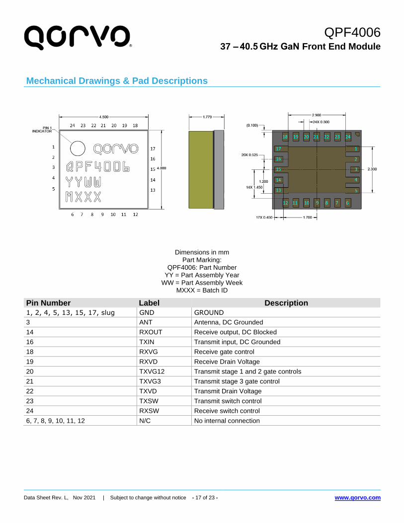
The compact 4.5 mm x 4.0 mm surface mount package configuration is designed to meet the tight lattice spacing requirements for phased array applications. The QPF4006 is fabricated on Qorvo’s 0.15um GaN on
SiC process. It is housed in an air-cavity laminate package
with an embedded copper heat slug. The copper slug,
coupled with a low thermal resistance die-attach process,
allows the QPF4006 to operate at the extreme case
temperatures needed in phased array applications. Functional Block Diagram
Applications • 5G Wireless Base stations and terminals
• Point to Point Communications
Part No. Description QPF4006TR7 Tape and Reel, 7", Qty 250
QPF4006EVB03 QPF4006 Evaluation Board, Qty 1
Product Features • Frequency Range: 37 – 40.5 GHz
• RX Noise Figure: 4.2 dB
• RX Small Signal Gain: 18 dB
• RX Saturated Power: 17 dBm
• RX TOI : 20 dBm @ - 5 dBm Pin / tone
• TX Small Signal Gain: 23 dB
• TX Saturated Power: 33 dBm
• TX TOI: 42 dBm @ 24 dBm Pout / tone
• TX ACPR: 32dBc @ 24dBm average Pout 2
• TX Linearity: 4% EVM @ 24 dBm average Pout 2
• TX PAE: 7% @ 24 dBm average Pout. • Package Dimensions: 4.5 x 4.0 x 1.8 mm
Data Sheet Rev. L, Nov 2021 | Subject to change without notice - 2 of 23 - www.qorvo.com
Absolute Maximum Ratings
Parameter Value Drain Voltage (TXVD, RXVD) 28 V
Drain Current (TXID3+TXID12) 800 mA
Drain Current (RXID) 60 mA
Gate Voltage (RXVG, TXVG3, TXVG12) 0 to −5 V
Gate Current (RXIG, TXIG3, TXIG12) 20 mA
Switch Control Voltage (TXSW, RXSW) 0 to 28 V
Switch Control Current 20 mA
RF Input Power (All RF ports, 85 °C) 30 dBm
Channel Temperature, TCH 225 °C
Mounting Temperature (30 seconds) 260 °C
Storage Temperature −55 to 150 °C
Operation of this device outside the parameter ranges given above may cause permanent damage. These are stress ratings only, and functional operation of the device at these conditions is not implied. Extended application of Absolute Maximum Rating conditions to the device may reduce device reliability.
Normal Operating Conditions
Parameter Value
Drain Voltage 20 V
Drain Current (TXIDQ12 / TXIDQ3) 135 mA / 24 mA *
Drain Current (RX, IDQ) 15 mA
Gate Voltage (TXVG12/TXVG3) −2 V / -2.4 V
Gate Voltage (RXVG) -2 V
Control Voltage (TXSW, RXSW) TXSW = 0 V, RXSW = 20V (RX on, TX off) TXSW = 20 V, RXSW = 0V (RX off, TX on)
Operating Temperature Range −40 to 95 °C
Gate voltage shown are typical, can be adjusted to set required drain current. Electrical specifications are measured at specified test conditions. Specifications are not guaranteed over all recommended operating conditions.
* Other current settings: 45 / 60 mA = 105 mA; 90 / 120 mA = 210 mA; 135 / 180 mA = 315 mA (gate controls combined together).
Data Sheet Rev. L, Nov 2021 | Subject to change without notice - 18 of 23 - www.qorvo.com
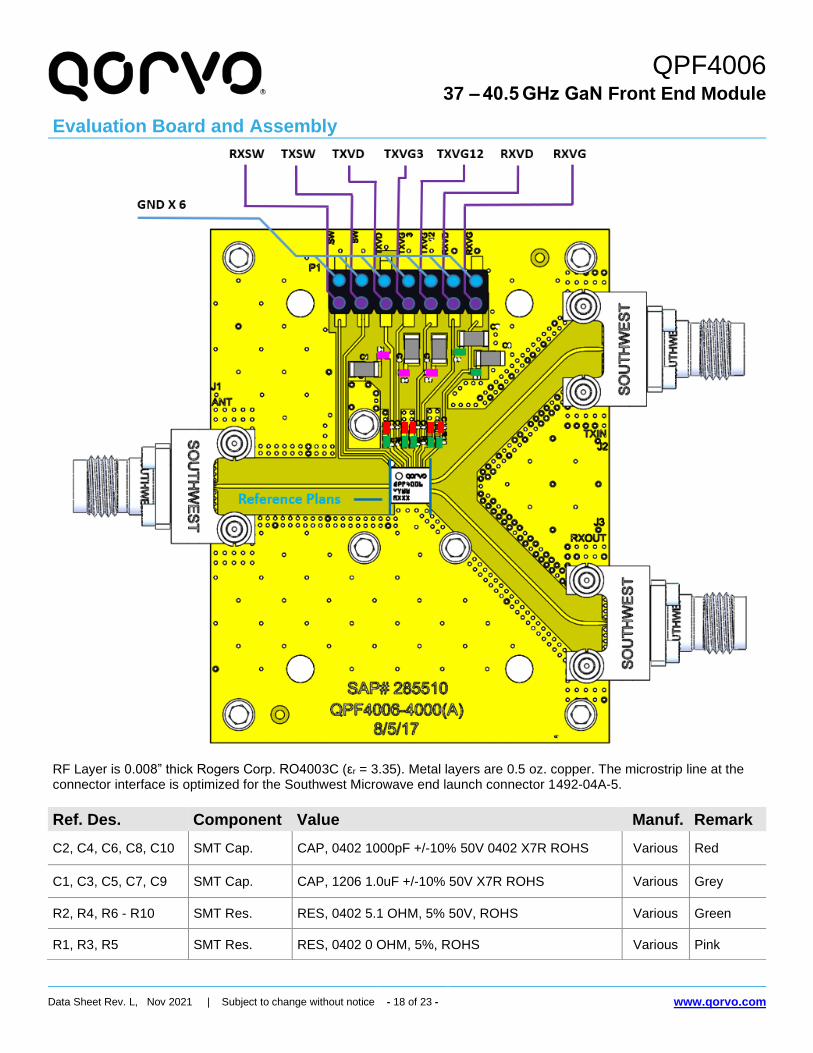
Evaluation Board and Assembly
RF Layer is 0.008” thick Rogers Corp. RO4003C (εr = 3.35). Metal layers are 0.5 oz. copper. The microstrip line at the connector interface is optimized for the Southwest Microwave end launch connector 1492-04A-5.
Ref. Des. Component Value Manuf. Remark
C2, C4, C6, C8, C10 SMT Cap. CAP, 0402 1000pF +/-10% 50V 0402 X7R ROHS Various Red
Data Sheet Rev. L, Nov 2021 | Subject to change without notice - 19 of 23 - www.qorvo.com
Application Circuit
Bias-up Procedure Bias-down Procedure
1. Set drain supply TXVD limit to 700 mA, RXVD limit to 50 mA, gate and control supply limit to 10 mA each.
1. Turn off RF signal
2. Set TXVG12, TXVG3, RXVG to −5 V 2. Set TXVG12, TXVG3 and RXVG to −5 V
3. Set TXSW = 20 V (or 0 V), RXSW = 0 V (or 20 V) 3. Set VD = 0 V
4. Set VD = +20 V 4. Turn off drain supply
5. For TX, adjust TXVG12 to get TXID12 current, then adjust TXVG3 to achieve required total drain current; For RX, adjust RXVG to achieve required drain current.
MSL – Convection Reflow 260 °C 3 JEDEC standard IPC/JEDEC
J-STD-020
RoHS Compliance This product is compliant with the 2011/65/EU RoHS directive (Restrictions on the Use of Certain Hazardous Substances in Electrical and Electronic Equipment), as amended by Directive 2015/863/EU. This product also has the following attributes:
• Lead Free
• Antimony Free
• TBBP-A (C15H12Br402) Free
• PFOS Free
Contact Information For the latest specifications, additional product information, worldwide sales and distribution locations:
Important Notice The information contained herein is believed to be reliable; however, Qorvo makes no warranties regarding the information contained herein and assumes no responsibility or liability whatsoever for the use of the information contained herein. All information contained herein is subject to change without notice. Customers should obtain and verify the latest relevant information before placing orders for Qorvo products. The information contained herein or any use of such information does not grant, explicitly or implicitly, to any party any patent rights, licenses, or any other intellectual property rights, whether with regard to such information itself or anything described by such information. THIS INFORMATION DOES NOT CONSTITUTE A WARRANTY WITH RESPECT TO THE PRODUCTS DESCRIBED HEREIN, AND QORVO HEREBY DISCLAIMS ANY AND ALL WARRANTIES WITH RESPECT TO SUCH PRODUCTS WHETHER EXPRESS OR IMPLIED BY LAW, COURSE OF DEALING, COURSE OF PERFORMANCE, USAGE OF TRADE OR OTHERWISE, INCLUDING THE IMPLIED WARRANTIES OF MERCHANTABILITY AND FITNESS FOR A PARTICULAR PURPOSE.
Without limiting the generality of the foregoing, Qorvo products are not warranted or authorized for use as critical components in medical, life-saving, or life-sustaining applications, or other applications where a failure would reasonably be expected to cause severe personal injury or death.