Quantitative Phase Imaging of Magnetic Nanostructures Using Off-Axis Electron Holography by Kai He A Dissertation Presented in Partial Fulfillment of the Requirements for the Degree Doctor of Philosophy Approved November 2010 by the Graduate Supervisory Committee: Martha R. McCartney, Co-Chair David J. Smith, Co-Chair Ralph V. Chamberlin Peter A. Crozier Jeff Drucker ARIZONA STATE UNIVERSITY December 2010
Transcript
Quantitative Phase Imaging of Magnetic Nanostructures
Using Off-Axis Electron Holography
by
Kai He
A Dissertation Presented in Partial Fulfillment of the Requirements for the Degree
Doctor of Philosophy
Approved November 2010 by the Graduate Supervisory Committee:
Martha R. McCartney, Co-Chair
David J. Smith, Co-Chair Ralph V. Chamberlin
Peter A. Crozier Jeff Drucker
ARIZONA STATE UNIVERSITY
December 2010
ABSTRACT
The research of this dissertation has involved the nanoscale quantitative
characterization of patterned magnetic nanostructures and devices using off-axis electron
holography and Lorentz microscopy. The investigation focused on different materials of
interest, including monolayer Co nanorings, multilayer Co/Cu/Py (Permalloy, Ni81Fe19)
spin-valve nanorings, and notched Py nanowires, which were fabricated via a standard
electron-beam lithography (EBL) and lift-off process.
Magnetization configurations and reversal processes of Co nanorings, with and
without slots, were observed. Vortex-controlled switching behavior with stepped
hysteresis loops was identified, with clearly defined onion states, vortex states, flux-
closure (FC) states, and Ω states. Two distinct switching mechanisms for the slotted
nanorings, depending on applied field directions relative to the slot orientations, were
attributed to the vortex chirality and shape anisotropy. Micromagnetic simulations were
in good agreement with electron holography observations of the Co nanorings, also
confirming the switching field of 700–800 Oe.
Co/Cu/Py spin-valve slotted nanorings exhibited different remanent states and
switching behavior as a function of the different directions of the applied field relative to
the slots. At remanent state, the magnetizations of Co and Py layers were preferentially
aligned in antiparallel coupled configuration, with predominant configurations in FC or
onion states. Two-step and three-step hysteresis loops were quantitatively determined for
nanorings with slots perpendicular, or parallel to the applied field direction, respectively,
due to the intrinsic coercivity difference and interlayer magnetic coupling between Co
and Py layers. The field to reverse both layers was on the order of ~800 Oe.
Domain-wall (DW) motion within Py nanowires (NWs) driven by an in situ
magnetic field was visualized and quantified. Different aspects of DW behavior,
i
including nucleation, injection, pinning, depinning, relaxation, and annihilation, occurred
depending on applied field strength. A unique asymmetrical DW pinning behavior was
recognized, depending on DW chirality relative to the sense of rotation around the notch.
The transverse DWs relaxed into vortex DWs, followed by annihilation in a reversed
field, which was in agreement with micromagnetic simulations.
Overall, the success of these studies demonstrated the capability of off-axis
electron holography to provide valuable insights for understanding magnetic behavior on
the nanoscale.
ii
This dissertation is dedicated to my parents,
who made everything possible.
iii
ACKNOWLEDGMENTS
I would like to express most sincere thanks to my advisors Professor Martha R.
McCartney and Regents’ Professor David J. Smith for their esteemed support and
guidance that made everything I achieved toward my PhD degree possible. Their open
minds, unlimited enthusiasm, precise insights and meticulous attitudes towards doing
research have educated me with good characteristics and discipline necessary for my
future career. I would also like to thank my dissertation committee members, Professors
Ralph Chamberlin, Peter Crozier, and Jeff Drucker, for their generous time and helpful
suggestions.
I would like to acknowledge the faculty and staff members as well as the use of
facilities in the John M. Cowley Center for High Resolution Electron Microscopy
(CHREM) and the Center for Solid State Electronics Research (CSSER) at Arizona State
University. Special thanks are due to Karl Weiss and Grant Baumgardner in CHREM,
and to Dr. Stefan Myhajlenko and Arthur Handugan in CSSER, for their technical
support and assistance throughout my research. The financial support from US
Department of Energy (Grant No. DE-FG02-04ER46168) is gratefully acknowledged.
I appreciate our collaborators Prof. J. Cumings (University of Maryland) and Dr.
J. Shaw (NIST) who provided samples, expertise, and personal concerns during my PhD
research. I also thank my colleagues at ASU, especially Dr. Hua Wang for training me on
cleanroom facilities, and Samuel Tobler for coating TEM samples.
Particular thanks and best wishes go to all the group members — Dr. Lin Zhou,
Dr. Nipun Agarwal, Dr. Changzhen Wang, Dr. Titus Leo, Dr. M.G. Han, Dr. Suk Chung,
Dr. David Cullen, Luying Li, Lu Ouyang, Wenfeng Zhao, Michael Johnson, Allison
Boley, Sahar Hihath, Jae Jin Kim, Aram Rezikya, Dinghao Tang, Dexin Kong, and et al.
for their friendship and kindness. My experiences with the “M&D Gang” have brought
iv
me a lot of joyful memories.
I appreciate the China Scholarship Council and the Ministry of Education for
awarding me the prestigious “Chinese Government Award for Outstanding Self-Financed
Students Abroad” towards my achievements during the Ph.D. studies. This recognition
from my mother country is the highest honor to inspire me heading forward.
Last but not least, I express the most heartfelt gratitude to my family, for their
infinite love and support that I could never pay back.
v
TABLE OF CONTENTS
Page
LIST OF TABLES............................................................................................................. ix
LIST OF FIGURES ............................................................................................................ x
According to their different response (so-called susceptibility χ) to an applied magnetic
field, materials are classified as diamagnetic, paramagnetic, ferromagnetic,
antiferromagnetic, and ferrimagnetic.
Our particular interest here is in ferromagnetic materials, such as iron, cobalt,
nickel, and their alloys. The magnetic moments in ferromagnetic materials are
1
spontaneously aligned in a regular manner, resulting in strong net magnetization even
without any applied field. Ferromagnetic materials have the property of hysteresis, which
can be technically characterized by a hysteresis loop, plotting out magnetization M (or
magnetic induction B) versus applied field H. Figure 1.1 shows a typical hysteresis loop
of a ferromagnetic material. The ferromagnet is initially not magnetized, and application
of the field H causes magnetic induction to increase in the field direction. If H is
increased indefinitely the magnetization eventually reaches saturation at a value which is
designated as Ms. When the external field is reduced to zero, the remaining magnetic
induction is called the remanent magnetization Mr. The magnetic induction can be
reduced to zero by applying a reverse magnetic field of strength Hc, which is known as
the coercivity.
Figure 1.1. Typical hysteresis loop of a ferromagnetic material.
2
The shape of a hysteresis loop reflects the properties of the ferromagnet. The area
inside the hysteresis is proportional to the energy needed to rotate the magnetic moments.
Based on the strength of the coercive field, ferromagnets can be roughly defined as hard
or soft magnetic materials. Hard (or permanent) magnets have coercivity as high as 2×10⁶
A/m (or 25000 Oe), and are widely used in electric motors, generators, loudspeakers,
frictionless bearings, magnetic levitation systems, and various forms of holding magnets
such as door catches. Soft magnets have much lower coercivity such as 1.0 A/m (or 12
mOe), and are mainly used in transformers, inductors, and magnetic sensors. Between
these two extremes are magnetic recording media, which require medium coercivity
(typically ranging from 104 A/m to 105 A/m), high Mr/Ms ratio, and good squareness of
hysteresis loop so as to ensure a sharp binary transition with low noise.
Two additional important concepts important for understanding the behavior of
magnetic materials are magnetic domains and domain walls (DWs). A magnetic domain
describes a region within a material which has uniform magnetization. The regions
separating magnetic domains are called DWs where the direction of the magnetization
rotates, usually coherently, from one domain to the adjacent domain [5]. The existence of
domains is a consequence of energy minimization [6]. Figure 1.2 shows schematics that
illustrate DW structures and domain configurations. To reduce the magnetostatic (MS)
energy, the spins inside the Bloch wall rotate through the plane of the wall, unlike the
Néel wall where the spins rotate in the plane of the wall. As shown in Figure 1.2 (c) – (f),
the introduction of 180° DWs reduces the MS energy but raises the DW energy, whereas
90° closure DWs can eliminate MS energy but increase the DW energy. Closure domain
formation is favored for large magnetization, small anisotropy, and small wall energy.
3
(a) Bloch wall (b) Néel wall
(c) Single domain (d) Multidomain (e) Multidomain (f) Closure domainHigh MS energy Lower MS energy Low MS energy No MS energy No DW energy Low DW energy Higher DW energy High DW energy
Figure 1.2. Schematic of DW structures and domain configurations. (a) Bloch wall; (b)
Néel wall; (c) – (f) domain configurations, where closure domain (f) has lowest energy.
1.1.2. Development of magnetic storage
Magnetic storage was first suggested by Oberlin Smith in 1888 [7]. However, the
first working magnetic recorder was invented in 1898 by Valdemar Poulsen, who
recorded a signal on a wire wrapped around a drum [8]. It was another three decades
before Fritz Pfleumer in 1928 developed the first magnetic tape recorder [9]. Early
magnetic storage devices were designed to record analog audio signals. Modern digital
recording for computer information storage was developed by IBM and the first magnetic
hard disk drive (HDD), which became available in 1957, had a data storage density of
only 2000 bit/in2 [10]. Since then, the data storage density has increased by many orders
of magnitude. Today, the present storage density is approaching 500 Gbit/in2. The rate of
increase in storage density has accelerated dramatically in recent years due to a new
4
generation of thin film recording media, and advanced read/write heads with improved
signal-to-noise ratio (SNR), as illustrated in the HDD road map shown in Figure 1.3.
Since data is being stored magnetically, the intrinsic property of
superparamagnetism will become a major limitation for conventional longitudinal
recording media as grain sizes get smaller and smaller. Thus, the energy required to
change the direction of the magnetic moment of a particle becomes comparable to the
ambient thermal fluctuations, which means that randomization of the domain orientations
becomes significant and data would be lost.
In recent years, new techniques such as bit-patterned recording, perpendicular
recording, thermal-assisted magnetic recording, and racetrack memory, have been
proposed for achieving higher storage density [11–13]. Two of these promising
candidates, namely, patterned recording media and racetrack memory, are described in
the following sections.
Figure 1.3. Road map of magnetic recording technology [10].
5
1.2. Nanopatterned Magnetic Recording Media
Figure 1.4 shows schematics of conventional longitudinal thin-film media,
patterned media and perpendicular media. In longitudinal thin-film media, each bit cell
may contain tens or hundreds of grains, which are separated by the transitions between
oppositely magnetized regions. In patterned media, single domain bits, which can be
either polycrystalline or single crystal, are defined with period p. The media consists of
arrays of such elements, each of which has uniaxial magnetization lying either in-plane of
the film or perpendicular to the film. Depending on different magnetization states, each
element represents one binary bit (up – “1”; down – “0”).
of phase in (a); (e) magnetic induction map using color wheel as direction reference.
51
52
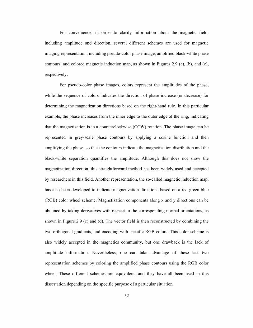
For convenience, in order to clarify information about the magnetic field,
including amplitude and direction, several different schemes are used for magnetic
imaging representation, including pseudo-color phase image, amplified black-white phase
contours, and colored magnetic induction map, as shown in Figures 2.9 (a), (b), and (e),
respectively.
For pseudo-color phase images, colors represent the amplitudes of the phase,
while the sequence of colors indicates the direction of phase increase (or decrease) for
determining the magnetization directions based on the right-hand rule. In this particular
example, the phase increases from the inner edge to the outer edge of the ring, indicating
that the magnetization is in a counterclockwise (CCW) rotation. The phase image can be
mplifying the phase, so that the contours indicate the magnetization distribution and the
black-white separation quantifies the amplitude. Although this does not show the
magnetization direction, this straightforward method has been widely used and accepted
by researchers in this field. Another representation, the so-called magnetic induction map,
has also been developed to indicate magnetization directions based on a red-green-blue
(RGB) color wheel scheme. Magnetization components along x and y directions can be
obtained by taking derivatives with respect to the corresponding normal orientations, as
shown in Figure 2.9 (c) and (d). The vector field is then reconstructed by combining the
two orthogonal gradients, and encoding with specific RGB colors. This color scheme is
also widely accepted in the magnetics community, but one drawback is the lack of
amplitude information. Nevertheless, one can take advantage of these last two
representation schemes by coloring the amplified phase contours using the RGB color
wheel. These different schemes are equivalent, and they have all been used in this
dissertation depending on the specific purpose of a particular situation.
represented in grey-scale phase contours by applying a cosine function and then
a
53
ecimen plane is obtained by tilting the sample holder, as shown in Figure
2.10 (a)
specimen height.
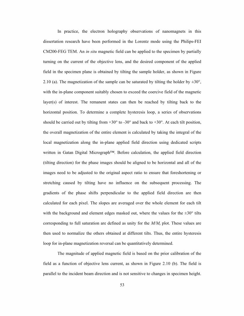
In practice, the electron holography observations of nanomagnets in this
dissertation research have been performed in the Lorentz mode using the Philips-FEI
CM200-FEG TEM. An in situ magnetic field can be applied to the specimen by partially
turning on the current of the objective lens, and the desired component of the applied
field in the sp
. The magnetization of the sample can be saturated by tilting the holder by ±30°,
with the in-plane component suitably chosen to exceed the coercive field of the magnetic
layer(s) of interest. The remanent states can then be reached by tilting back to the
horizontal position. To determine a complete hysteresis loop, a series of observations
should be carried out by tilting from +30° to -30° and back to +30°. At each tilt position,
the overall magnetization of the entire element is calculated by taking the integral of the
local magnetization along the in-plane applied field direction using dedicated scripts
written in Gatan Digital Micrograph™. Before calculation, the applied field direction
(tilting direction) for the phase images should be aligned to be horizontal and all of the
images need to be adjusted to the original aspect ratio to ensure that foreshortening or
stretching caused by tilting have no influence on the subsequent processing. The
gradients of the phase shifts perpendicular to the applied field direction are then
calculated for each pixel. The slopes are averaged over the whole element for each tilt
with the background and element edges masked out, where the values for the ±30° tilts
corresponding to full saturation are defined as unity for the M/Ms plot. These values are
then used to normalize the others obtained at different tilts. Thus, the entire hysteresis
loop for in-plane magnetization reversal can be quantitatively determined.
The magnitude of applied magnetic field is based on the prior calibration of the
field as a function of objective lens current, as shown in Figure 2.10 (b). The field is
parallel to the incident beam direction and is not sensitive to changes in
54
The default value for objective lens current in normal operating mode is ~9880 mA,
corresponding to a vertical magnetic field of ~1.90 T (19000 Oe). The residual field at
the specimen plane is unaffected by excitation of the Lorentz minilens, and negligible in
most cases.
Several important parameters need to be considered for holographic imaging,
including fringe spacing, fringe overlap, fringe visibility (contrast), and field of view
[12]. These parameters can be controlled by suitable combinations of accelerating
voltage, extraction voltage, and biprism voltage. To ensure coherent illumination, the
microscope is usually operated at 200 kV with gun lens 5 and spot size 1 setup. The
fringe visibility is quite sensitive to the extraction voltage, with the optimum value of
~3.78 kV. The biprism voltage determines both the fringe spacing and the region of
Figure 2.10. (a) Schematic diagram showing the use of specimen tilt to provide the in-
plane component of the applied field needed for in situ magnetization reversal
experiments. (b) Hall probe measurements of magnetic field in specimen plane of Philips
CM200 as function of objective lens current [2].
overlap, and is typically biased to a potential of 100 V. The holographic fringe contrast is
defined by
minmax
minmax II −=μ (2.8) II +
where I
The term “spin ice” refers to a magnetic system with geometrical frustrated
interactions, where the local disorder of magnetic moments appears in the ordered lattice
structure [19]. Recent experiments have provided evidence suggesting the existence of
deconfined magnetic monopoles in these materials, with properties analogous to the
hypothetical magnetic monopoles postulated to exist in vacuum [20–26].
max and Imin are maximum and minimum intensity, respectively, in the region of
overlap of the interference fringes. The contrast can be measured by an averaged line
profile across the fringes, and typical fringe contrast of ~40% can be obtained, which is
more than adequate for holographic imaging and phase reconstruction.
2.5. Examples of Quantitative Phase Imaging
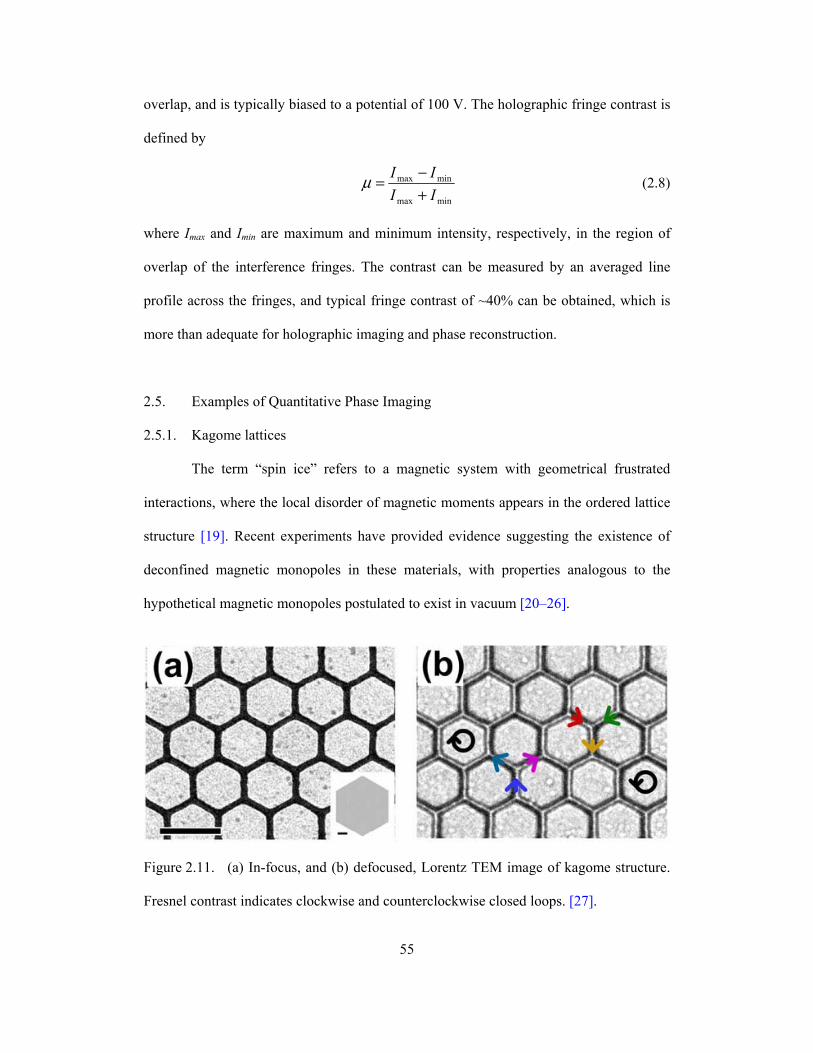
2.5.1. Kagome lattices
Figure 2.11. (a) In-focus, and (b) defocused, Lorentz TEM image of kagome structure.
Fresnel contrast indicates clockwise and counterclockwise closed loops. [27].
55
56
f an artificial spin ice system using a two-dimensional (2D) kagome lattice
[27]. Lorentz imaging was used to demonstrate the local ice r
occurrence of long-range dipolar interactions, as illustrated by Figure 2.11. However,
conventional EBL
technique, followed by metal deposition of Py (Ni80Fe20) and lift-off [27]. The designed
erent lengths and widths, and separated
ctions. The Py layer is nominally 23 nm in thickness.
the top-right to
the bottom-left direction, and then reverse saturated along the opposite direction.
Holograms in the two opposite remanent states were thus obtained. The corresponding
reconstructed phase images are shown in Figure 2.12 (a) and (b). Line profiles from the
same regions but in opposite magnetic states are shown plotted, and the linear slopes
caused by the magnetic fields only appear at the central part of the wire. However, these
are smeared out at the wire edges due to the nonuniform thickness (or MIP) contribution.
A phase image showing the pure magnetic component could be achieved by the
t constant
Cumings and his group at the University of Maryland have recently described
realization o
ule and as well as the
many details remain to be determined about this topic. As a collaborative project,
electron holography was used to characterize some typical spin-ice samples. These results
also represent an example of quantitative phase imaging.
The kagome-structured spin ice samples were fabricated using
patterns included hexagonal honeycombs with diff
three-fold “Y” shaped jun
The kagome lattice having ~1μm diagonal separation and ~110nm lattice width
was first observed, as shown in Figure 2.12. Because of the limited region of coherent
illumination for electron holography, only the edges of the kagome lattice could be
observed, but some irregular branch shapes were present in such regions due to errors
during fabrication. The initial saturation magnetic field was applied from
subtraction of images, as shown in Figure 2.12 (c). Line profiles indicate a linear slope
across the entire wire, but the slope remains flat elsewhere, suggesting tha
Figure 2.12. Phase images of kagome lattice composed of Py and corresponding line
profiles in remanent state with: (a) saturation field pointing to bottom-left; (b) saturation
field pointing to top-right; and (c) pure magnetic contribution. (d) 8× amplified phase
contours, (e) magnetic induction map, and (f) magnetic contour map, converted from (c).
57
58
magnetization is uniformly distributed within the wire, and that any edge effects have
been completely removed. Measurements showed that the slope of the phase shifts in all
three wires was 0.035±0.001 rad/nm. Since the thickness of the lattice is nominally 23
nm, the corresponding magnetic induction is calculated to be 1.00±0.03 T, which is a
reasonable value for the saturation magnetization of Py. The phase image was converted
into phase contours, magnetic induction map, and magnetic contour map, as shown in
Figure 2.12 (d)–(f), respectively. These clearly indicate the directions of magnetization
and the surrounding fringing fields.
At this junction of the kagome lattice, the magnetic flux comes “in” from the top-
right, and then goes “out” through the left and bottom-right, thus forming an “in-out-out”
configuration. The 2D mapping of the magnetic phase contours within lattice wires and
the external fringing fields confirmed that the magnetization contours were continuous,
and in closure loops, indicating that no magnetic monopoles were present in this area.
Similar characterization was carried out on another kagome lattice with smaller
dimensions of ~500 nm across the diagonal and ~65 nm in lattice width. The
corresponding phase images and magnetic induction maps are shown in Figure 2.13. The
magnetic induction map in Figure 2.13 (b) clearly shows four junctions with different
configurations, where one “in-out-out” configuration (I) is associated with three “in-in-
out” configurations (II, III, and IV). However, only magnetic flux closures, but no
evidence for monopoles, were found in the kagome lattice.
Figure 2.13. Phase contour map (12× amplified), magnetic induction map, and magnetic
contour map of (a)–(c) 500-nm-diagonal kagome lattice, and (d)–(f) enlarged box area,
respecti
and residual chemicals, were
isible on the nitride membrane. These could cause considerable noise in both imaging
and reconstruction of the phase shifts. The boxed area was placed in the region of
coherent illumination and a hologram was obtained, as shown in Figure 2.14 (b). The
reconstructed phase contour map, magnetic induction map, and magnetic contour map are
shown in Figures 2.14 (c)–(e), respectively. Noise signals caused by the contamination,
vely. Magnetization directions indicated by color wheel.
Individual Y-junctions with a 3-fold symmetry shape were observed in order to
investigate any differences in properties between separated junctions and junctions in a
continuous lattice. Figure 2.14 (a) shows the Lorentz image of as-fabricated Y junctions.
Each branch of the Y-junction is 100 nm in width and 400 nm in length. Contaminations
from EBL and lift-off processes, such as metal particles
v
59
60
appearing as big dots or vortices in the phase contour map, did not obscure the result that
the individual Y-junction was in an “in-in-out” configuration, with continuous magnetic
flux.
Although no obvious evidence was found in these studies to confirm the
existence of magnetic monopoles, this investigation of kagome lattices demonstrated the
capability of electron holography for observing and quantifying static magnetic fields on
the nanometer scale.
Figure 2.14. (a) Lorentz TEM image of as-fabricated Y-junctions. (b) Hologram of an
individual Y-junction in boxed area of (a). (c) Phase contour map (12× amplified), (d)
magnetic induction map, and (e) magnetic contour map, respectively, of the Y-junction.
61
a topic of considerable interest with the emergence of new technological
applicat
ets of triangular shape suggested two equilibrium states at
remanence. One was the so-called “Y” state, where the magnetization fanned in from two
corners towards the third along the bisector; the other was referred as the “buckle” state,
where the magnetization bent toward one of the corners parallel to the edge, as indicated
schematically in Figure 2.15 [29]. Particular attention has been given to these triangle
magnets as a function of different shapes and external fields, in particular to find the
magnetization reversal mechanism(s) and any related spin-wave confinement caused by
internal fields [28–31]. Representative triangle-shaped magnets have been investigated in
collaboration with Shaw (NIST) and Hillebrands (University of Kaiserslautern).
2.5.2. Ferromagnetic triangles
The dynamic properties of ferromagnetic magnets with different shapes have
been
ions of patterned magnetic recording media. Uniform magnetization is desirable
but oftentimes unachievable in polygonal particles due to shape anisotropy and high-
order configurational anisotropy [28]. For example, micromagnetic simulations for
nanoscale ferromagn
Figure 2.15. Micromagnetic simulations showing remanent configuration in: (a) Y state
in a sharp triangle; and (b), (c) buckle states in rounded triangles [29].
62
bricated using standard EBL and etching methods. The
patterne
electron
hologra y has been demonstrated to provide useful insights for both static and dynamic
aspects of nanoscale magnetic materials.
The Py triangles were fa
d elements were all of the same thickness of 10 nm, but with different lateral
dimensions, nominally, 1×1.5, 1×1, 0.5×1.5, 0.5×1 (base × height, unit in µm), as shown
by the Lorentz TEM images in Figures 2.16 (a)–(d), respectively.
Each of the magnetization states of these elements during an entire hysteretic
switching process was recorded at a series of tilting positions with respect to the vertical
applied magnetic field. Figure 2.16 shows seven different states (1–7) for each triangle
(a–d) as a function of applied field strength. The two proposed states were identified,
with the buckle states visible at the remanence (a4, b4, c4, d4), whereas the Y states
occurred at the saturation fields (a7, b7, c7, d7). These results are in good agreement with
recent experimental and simulated results [29–31], although the proposed vortex mode
was not observed. Moreover, it was found that the critical fields for the transitions
between the two states varied depending on the different height-base ratios, which most
likely correlates with the shape and configurational anisotropy. Comprehensive
investigation for a better understanding is ongoing, but it can be concluded that
ph
Figure 2.16. Lorentz images of Py triangles with different sizes, and corresponding
phase contours (4× amplified) as function of in-plane applied field. Applied field along
the long axis of the triangles.
63
64
Referen s
[1] . A. McCord and M. J. Rooks, in Handbook of Microlithography, Micromachining, and Microfabrication Volume 1, edited by P. Rai-Choudhury,
PIE Optical Engineering Press, Bellingham, WA, Chapter 2, (1997).
[2] . E. Dunin-Borkowski, M. R. McCartney, B. Kardynal, M. R. Scheinfein, and D. J. Smith, J. Microsc. 200, 187 (2000).
[3] T. Schrefl, D. Suess, G. Hrkac, M. Kirschner, O. Ertl, R. Dittrich, and J. Fidler, in Advanced Magnetic Nanostructures, edited by D. J. Sellmyer and R. Skomski, Springer, New York, Chapter 4, (2006).
[4] T. L. Gilbert, Phys. Rev. 100, 1243 (1955).
[5] L. D. Landau and E. M. Lifshitz, Phys. Z. Sowietunion 8, 153 (1935).
[6] M. J. Donahue and D. G. Porter, OOMMF User's Guide Version 1.0, National Institute of Standards and Technology, Gaithersburg, MD (1999).
[7] J. N. Chapman, J. Appl. Phys.: D 17, 623 (1984).
[8] J. N. Chapman and A. K. Petford-Long, in Magnetic Microscopy of Nanostructures, edited by H. Hopster and H. P. Open, Springer-Verlag, Berlin-Heidelberg, Chapter 4, (2005).
[9] D. Shindo and T. Oikawa, Analytical Electron Microscopy for Materials Science, Springer-Verlag, Tokyo, Chapter 5, (2002).
[10] D. Gabor, Nature 161, 777 (1948).
[11] D. Gabor, Proc. Roy. Soc. London A197, 454 (1949).
[12] D. J. Smith and M. R. McCartney, in Introduction to Electron Holography, edited by E. Völkl, L. F. Allard and D. C. Joy, Kluwer Academic-Plenum Publishers, New York, Chapter 4, (1999).
[13] R. E. Dunin-Borkowski, M. R. McCartney, and D. J. Smith, in Encyclopedia of
Stevenson Ranch, CA, Chapter 7, (2004).
[14] M. R. McCartney and D. J. Smith, Annu. Rev. Mater. Res. 37, 729 (2007).
[15] H. Lichte, P. Formanek, A. Lenk, M. Linck, C. Matzeck, M. Lehmann, and P. imon, Annu. Rev. Mater. Res. 37, 539 (2007)
[16] . Tonomura, Surf. Sci. Rep. 20, 317 (1994).
[17] . E. Dunin-Borkowski, T. Kasama, A. Wei, S. L. Tripp, M. J. Hӱtch, E. Snoeck, nis, Microsc. Res. Tech. 64, 390 (2004).
ce
M
S
R
Nanoscience and Nanotechnology, edited by H. S. Nalwa, American Scientific
S
A
RR. J. Harrison, and A. Put
65
. McCartney, N. Agarwal, S. Chung, D.A. Cullen, M.-G. Han, K. He, L. Li, H. Wang, L. Zhou, D.J. Smith, Ultramicroscopy 110, 375 (2010).
[20] R. F. Wang, C. Nisoli, R. S. Freitas, J. Li, W. McConville, B. J. Cooley, M. S.
ature Phys. 5, 258 (2009).
, K. Kiefer, S. Gerischer, D. Slobinsky, and R. S. Perry, Science 326, 411 (2009).
[26] T. Fennell, P. P. Deen, A. R. Wildes, K. Schmalzl, D. Prabhakaran, A. T.
[27] Y. Qi, T. Brintlinger, and J. Cumings, Phys. Rev. B 77, 094418 (2008).
. Welland, J. Appl. Phys. 88, 5315 (2000).
[29] L. Thevenard, H. T. Zeng, D. Petit, and R. P. Cowburn, J. Appl. Phys. 106,
[31] F. Montoncello and F. Nizzoli, J. Appl. Phys. 107, 023906 (2010).
[18] M.R
[19] L. Pauling, J. Am. Chem. Soc. 57, 2680 (1935).
Lund, N. Samarth, C. Leighton, V. H. Crespi, and P. Schiffer, Nature 439, 303 (2006).
[21] C. Castelnovo, R. Moessner, and S. L. Sondhi, Nature 451, 42 (2008).
[22] O. Tchernyshyov, Nature 451, 22 (2008).
[23] L. D. C. Jaubert and P. C.W. Holdsworth, N
[24] M. J. P. Gingras, Science, 326, 375 (2009).
[25] D. J. P. Morris, D. A. Tennant, S. A. Grigera, B. Klemke, C. Castelnovo, R. Moessner, C. Czternasty, M. Meissner, K. C. Rule, J.-U. Hoffmann
Boothroyd, R. J. Aldus, D. F. McMorrow, and S. T. Bramwell, Science 326, 415 (2009).
[28] D. K. Koltsov, R. P. Cowburn, and M. E
063902 (2009).
[30] M. Jaafar, R. Yanes, A. Asenjo, O. Chubykalo-Fesenko, M. Vázquez, E. M. González, and J. L. Vicent, Nanotechnology 19, 285717 (2008).
CHAPTER 3
66
ORTEX-CONTROLLED
This chapter describes the electron holography investigation of remanent states
and magnetization reversal of monolayer Co nanorings, with and without slots. Vortex-
controlled switching behavior has been identified, which exhibits stepped hysteresis
on states, vortex states, flux-closure
due to their potential applications in high density data storage
for recording
urposes. As the lateral dimensions of the elements are scaled down to the hundreds to
ns of nanometers, their geometry plays an even more important role in determining the
magnetization configuration [4]. Designs based on simple shapes, such as squares,
rectangles, and other polygons, are not really suitable for data storage due to the
occurrence of irregular edge domains [4–7]. Circular disks can lead to stable
magnetization configurations, i.e., flux-closure (FC) states (often refereed to as vortices),
MAGNETIZATION CONFIGURATIONS AND V
SWTICHING BEHAVIOR OF Co NANORINGS
loops with specific well-defined states including oni
states, and omega states. Two distinct switching mechanisms, depending on the applied
field direction relative to the slot orientation, can be attributed to the vortex chirality and
shape anisotropy. Micromagnetic simulations have also been performed to confirm the
experimental observations. The major results of this study have been published elsewhere
[1, 2].
3.1. Introduction
Nanopatterned ferromagnetic (FM) elements have been intensively studied
during the past decade
technology [3]. A reproducible magnetization reversal process with well-defined
remanent states and narrow switching fields is obviously preferable
p
te
67
without any stray field, which thus minimizes any interaction between elements.
However, the presence of the central vortex limits their functionality by complicating the
switching process [8, 9].
Ring-shaped nanostructures are attracting interest because their circular geometry
can sup
out a slot [16–20]. In either of these geometries, the asymmetrical shape leads
predom antly to the onion-FC-onion transition via the formation and annihilation of
DWs. Local spin-vortex structures often appear during the magnetization reversal,
resulting in irregularities in the switching process and broadening of the switching field
distribution. Thus, better understanding and more precise control of the dynamics of
magnetic vortex structures are essential in order to improve the functionality of magnetic
nanostructures [13, 21–22]. Based on micromagnetic simulations, a vortex-dependent
magnetization process with a three-step hysteresis loop was proposed, which suggested
that spin-vortex structures had caused the transform from onion state to FC state [15].
However, no direct experimental evidence for this three-step reversal mechanism has
been previously reported.
In this chapter, Co nanomagnets with ring shapes were chosen for investigation,
where the slots were intended to introduce geometrical restrictions that would change the
port FC states, as well as eliminating the high-energy central vortex core that
causes irreproducibility during magnetization reversal [10–12]. Another common state
obtained in ring structures after saturation is the so-called “onion” or “bi-domain” state,
consisting of two semicircular head-to-head (HTH) domains separated by domain walls
(DWs) [13]. The switching process then occurs out via two different modes, namely,
coherent onion rotation or onion-FC-onion transition [14–16]. Several approaches have
been used to obtain controllable switching mechanisms via the introduction of
asymmetrical characteristics to the ring, including displacement of the central hole or
cutting
in
68
to silicon nitride TEM membrane windows using EBL and lift-
off proc
shape anisotropy and constrain any vortex excitations relative to regular rings. The
sample geometries are shown schematically in Figure 3.1. The 30-nm-thick Co elements
were fabricated directly on
ess, followed by deposition of another 3-nm-thick Ti layer in order to minimize
oxidation and to prevent electrostatic charging during TEM observation. In situ magnetic
fields with maximum in-plane components of ~1200 Oe at ±30° tilting positions were
applied parallel or perpendicular to the slot direction, and electron holography
observations to examine the remanent states and magnetization reversal were carried out
using the Lorentz TEM mode.
the geometry of Co nanoring and slotted Co nanoring,
grown on thi
nanoring; and (c) slotted nanoring.
Figure 3.1. Schematics showing
n silicon nitride TEM membranes: (a) Side view; and plan view of (b)
3.2. Remanent States and Switching Behavior of Co Nanorings
The as-prepared Co nanorings were observed with and without applied magnetic
field. Figure 3.2 (a) is a Lorentz image showing the nanorings with outer diameter of
~400 nm and inner diameter of ~150 nm. These nanorings were patterned into 3×3
arrays, with ~800-nm spacing between adjacent elements to minimize any interactions.
The reconstructed phase image of a Co nanoring observed at remanence is shown in
Figure 3.2 (b). Phase shifts due to the magnetic contributions were extracted using a pair
of holograms having opposite FC chirality, as shown in the contour map. The uniformly
Figure 3.2. (a) Lorentz TEM image showing Co nanoring array (Scale bar indicates
500 nm). (b) Reconstructed holographic phase image of an individual nanoring showing
re
y color wheel and overlaid arrows.
FC state at manence, with phase contour spacing of π/3. (c) Line profile from A to B.
(d) Experimental, and (e) simulated, magnetic induction maps of the Co nanoring.
Magnetization directions indicated b
69
70
The line
profile,
imulations, as shown in Figure 3.2 (e), and is in close agreement with the experimental
observation.
The switching behavior of the Co nanorings when taken through a complete
hysteresis cycle was then investigated in detail. Figure 3.3 shows the hysteresis loop for
an individual Co nanoring. This hysteresis loop was extracted from the experimental
holographic phase images, using images obtained at saturation for normalization to unity.
The details of these calculations were described earlier in section §2.4.2. The hysteresis
loop exhibited two steps, corresponding to transitions from the saturated onion state to
the FC state, and then to the reversed onion state. A double vortex appeared during the
onion-to-FC transition when the external field approached close to zero, but this did not
appear to affect the shape of the hysteresis loop, nor did it cause any obvious plateau. The
slight horizontal shift in the loop was attributed to a small zero error in sample tilting,
distributed contours demonstrate the FC magnetization rotation of the nanoring.
taken from position A to B, shows the linearity of the phase shifts within the
nanoring and almost constant phase in external areas. The effective magnetic thickness
was determined to be ~25 nm using phase gradient measurements and Equation 2.7. This
thickness value was less than the nominal amount, but it was then used in the subsequent
micromagnetic simulations. The phase image was converted into a magnetic induction
map, using a color wheel for denoting particular directions, as shown in Figure 3.2 (d).
The remanent induction map for the same structure, was calculated by OOMMF
s
however, this did not affect determination of the switching field which was found to be
~800 Oe.
Figure 3.3. Hysteresis loop of an individual Co nanoring where a–d correspond to
pecific states visible in phase images: (a) onion state at saturation; (b) excitation of
ouble-vortex; (c) FC state; (d) onion state at reverse saturation. Magnetization directions
dicated by overlaid white arrows. Applied field directions indicated by the black arrow.
s
d
in
71
72
Figures 3.3 (a)–(d) show representative phase images corresponding to the
magnetization states observed at different stages of the hysteresis loop, which are labeled
with a–d. These configurations were obtained from one half of the hysteresis loop, and
are opposite to those observed in the other half of the loop. The saturation configurations
with strong fringing fields corresponded to the onion state and the reversed onion state, as
shown in Figures 3.3 (a) and (d), respectively. By taking the color sequences into
account, the directions of magnetization can be determined, as indicated by the overlaid
arrows. Two vortices, both with clockwise (CW) chirality, were identified close to the
domain wall (DW) region of the onion configuration, as visible in Figure 3.3 (b). The
chirality of the vortex directly affects the evolution of the vortex and determines the
switching mechanism, as will be discussed in detail later. The double-vortex state was
formed as the external field approached the remanence condition, and it was then
eliminated leaving behind a flux-closure state with CW magnetization and minimal
fringing field, as shown in Figure 3.3 (c). The upper half of the element reversed first to
form the FC, followed by switching of the lower half to obtain the completely reversed
onion state. The presence of the FC configuration was visible as a flat plateau, and
stabilized the Co nanorings.
3.3. Remanent States and Switching Behavior of Slotted Co Nanorings
As-prepared Co slotted nanorings were observed with and without applied
magnetic field. Figures 3.4 (a) and (b) show Lorentz images of two sets of element arrays
with the slot orientations rotated by 90°. The in-plane magnetic field was applied along
the directions indicated by arrows, i.e., parallel to the slot direction in Figure 3.4 (a), and
perpendicular to the slot direction in Figure 3.4 (b). For convenience, the designations
SR1 and SR2 will be used to denote slotted rings with slot directions parallel, or
73
perpendicular, to the applied field direction, respectively. Typical elements in both arrays
were observed at the remanent state after initial saturation and removal of the applied
field, and the corresponding reconstructed phase images are shown in Figures 3.4 (c) and
(d). Observations showed that the remanent magnetization configurations exhibited onion
states when the initial saturation field was applied parallel to the slot orientation, whereas
FC states were preferentially obtained with the initial saturation direction perpendicular
to the slot direction.
Figure 3.4. Lorentz images of Co slotted nanorings, with slot directions (a) parallel,
and (b) perpendicular, to applied field directions (indicated by double arrow).
Reconstructed phase images showing individual Co elements at remanence: (c) onion;
and (d) FC state.
74
The switching behavior of the Co slotted nanorings through a complete hysteresis
cycle was also observed. Figure 3.5 compares hysteresis loops for Co nanorings with in-
plane field applied parallel, and perpendicular, to the slot direction. The inset schematics
indicate the different magnetization configurations of each state that occur during the
hysteresis cycle. For the shape SR1 with external field applied parallel to the slot, as
shown in Figure 3.5 (a), the hysteresis loop exhibited three steps, corresponding to
transitions between saturated onion state, vortex excitation, FC state, and reversed onion
state. Conversely, when the external field was applied perpendicular to the slot direction,
as shown in Figure 3.5 (b), the shape SR2 exhibited a simple one-step hysteresis loop
with good squareness, indicating that the magnetization of the slotted ring reversed
abruptly between FC states of opposite chirality. The switching fields were determined to
be ~800 Oe for the shape SR1 and ~700 Oe for the shape SR2. It is noteworthy that the
three-step hysteresis loop had been predicted by numerical simulations for ring-shaped
Py elements with similar dimensions [15]. However, these experimental results are the
first time that such evidence has been observed for Co slotted-ring elements.
Figure 3.6 shows representative phase images corresponding to the states at
different stages of the hysteresis loop labeled a–d in Figure 3.5 (a). The saturation
configurations corresponded to the onion state and the reversed onion state with strong
fringing fields, as shown in Figures 3.6 (a) and (d), respectively. As indicated by the
overlaid arrows, the magnetization direction in Figure 3.6 (a) was counterclockwise
(CCW) in the upper half of the nanoring, and CW in the lower half, and vice versa in
Figure 3.6 (d). A vortex with CCW chirality was identified close to the domain wall
region of the onion configuration, as visible in Figure 3.6 (b). The precise location of this
vortex formation could be related to local defects of the sample or possible geometrical
asymmetry between the two branches. The vortex was formed as the external field
75
Figure 3.5. (a) Three-step, and (b) one-step, hysteresis loops for Co elements with
applied field parallel, and perpendicular, to the slot direction, respectively. The inset
schematics indicate the different magnetization configurations that occurr during the
hysteresis cycle.
76
Figure 3.6. Phase images of Co nanoring (SR1) illustrating the magnetization
configurations for corresponding states in the hysteresis loop in Figure 3.5 (a): (a) onion
state; (b) excitation of vortex at remanence; (c) FC state; and (d) reversed onion state.
Figure 3.7. Phase images of Co nanoring (SR2) illustrating the magnetization
configurations for corresponding states in the hysteresis loop shown in Figure 3.5 (b): (a)
Ω state; (b) FC state of CW; (c) FC state of CCW; and (d) reversed Ω state.
77
approached the remanence condition, and it was then eliminated leaving behind a flux-
closure state with CW magnetization and a weak fringing field, as shown in Figure 3.6
(c). The upper half of the element reversed first to form the FC state, followed by
switching of the lower half to complete the FC-to-onion transition. The presence of the
FC configuration stabilized the Co element, visible as a flat plateau, which was also
responsible for the increase of the switching field to ~800 Oe, relative to ~700 Oe for the
shape SR2. Micromagnetic simulations indicated that the transition from onion state to
FC state was dependent on the evolution of the vortex. Once the vortex was formed, it
could move in two alternative directions: either it would take the shorter route to the end
of the associated branch, or else take the longer route towards the other end. Meanwhile,
that branch also reversed its magnetization to reach the flux-closure state. The shorter
distance would be preferable, although the other case could occasionally occur, as
indicated in Figure 3.6 (c).
Figure 3.7 shows phase images corresponding to the states labeled a–d in the
hysteresis loop of Figure 3.5 (b). When the field was applied perpendicular to the slot
direction, the saturation configurations of shape SR2 appeared as “Ω” states, which were
FCs with magnetization twisted to the direction of the external field at the slot edges, as
shown in Figures 3.7 (a) and (d). As the applied field was reduced below the coercivity
(~700 Oe), the magnetization relaxed to form a FC state with CW chirality, as visible in
Figure 3.7 (b). When the applied field was decreased further to a negative coercivity
value, the magnetization of the slotted ring reversed abruptly from the CW FC state to the
CCW chirality, as visible in Figure 3.7 (c).
78
s a more sheared shape than that in Figure 3.8 (c).
3.4. Comparison Between Experimental Results and Simulations
Micromagnetic simulations were systematically performed for both experimental
geometries of regular and slotted rings, with external fields applied parallel or
perpendicular to the slot direction, where applicable. The experimental and simulated
results are compared in each situation, and also summarized for all three shapes of ring,
SR1, and SR2. Figures 3.8 (a)–(c) show the hysteresis loops obtained from experimental
electron holograms of the nanoring, and shapes SR1 and SR2, respectively. The coercive
fields were determined by averaging the values from both forward and backward cycles
of each specific element, as summarized in Table I. Simulated hysteresis loops from
micromagnetic modeling for the ring, SR1, and SR2, are shown in Figures 3.8 (d)–(f),
respectively. From comparisons between the corresponding loops, it is apparent that the
experimental and simulated results are in close quantitative agreement, except that the
loop in Figure 3.8 (f) exhibit
Table 3.1. Switching fields measured from experimental and simulated hysteresis loops.
Switching fields (Oe) Sample
Experimental Simulated
Ring ~800 950±50
SR1 ~800 800±100
SR2 ~700 850±50
Figure 3.8. (a)–(c) Experimental, and (d)–(f) simulated, hysteresis loops for Co
anoring, slotted nanoring with applied field parallel to slot (SR1), and slotted nanoring
ith applied field perpendicular to slot (SR2), respectively.
n
w
79
80
The primary difference in behavior between these three geometries is that shape
SR2 shows a one-step hysteresis loop, whereas shape SR1 and the regular nanoring
exhibit multiple steps in their loops. These steps represent transitions between distinct
and well-defined magnetization configurations, including onion state, vortex formation,
and FC state. Moreover, because the occurrence of these steps corresponds to different
fields, the elements show different remanent configurations. The representative states, as
indicated by letter labels, are illustrated in Figure 3.9: the magnetization configurations,
and colors (denoting directions), for the corresponding pairs of measured and simulated
images are in excellent agreement. Detailed information about the behavior observed for
each specific geometry has already been given. However, it is useful to compare the
magnetization reversal and vortex evolution, which were most often observed in
numerous experiments for the different shapes.
For the regular ring shape, when the strength of the applied field is decreased
from initial saturation, vortices gradually form at the DW regions to minimize the total
energy via reduction of the fringing field. A double-vortex (1b and 1f) forms within the
onion configuration, when the field is close, but not equal, to zero. These two vortices,
having the same CCW chirality, move toward each other, and then annihilate to form a
simple CCW FC state at remanence (1c and 1g). Eventually, the FC state becomes a
reverse onion state by reversal of the lower half-ring after the field exceeds the switching
value (1d and 1h). This latter transition took place too quickly to catch any intermediate
states during the observation. Thus, the overall magnetization switching process takes
place via the onion-FC-onion mechanism, which is consistent with previous numerical
simulations and experimental observations [14, 17].
Figure 3.9. Magnetic induction maps for (1) Co ring, (2) SR1, and (3) SR2, comparing
corresponding states in Figure 3.8. Applied field along horizo
the experimental results (upper row) and simulations (lower row). Letter labels refer to
ntal direction. Contour
spacing of π/2. Magnetization directions indicated by color wheel or overlaid arrows.
81
82
The SR1 shape exhibits an onion state at saturation (2a and 2e), and undergoes an
onion-FC-onion switching behavior, which is similar to that of the regular ring, because
both shapes are symmetrical with respect to the applied field direction. However, since
the presence of the slot breaks the horizontal symmetry in the region where a vortex is
expected, only one vortex is formed at remanence during the onion-to-FC transition, as
was indicated in images 2b and 2f. This single vortex, with clockwise (CW) chirality,
moves downward through the entire lower half-branch, and then annihilates at the slot
edge to form the CW FC configuration (2c and 2g). The longer path for this single vortex,
which requires more energy from the applied field, provides an explanation for the
postponed FC appearance relative to that observed for the regular nanoring. Finally, the
upper half-branch reverses to reach the reverse onion state (2d and 2h), although no
information has been observed that shows the details of this switching process.
In contrast to the multi-step switching behavior for the elements above, the SR2
shape experiences a simple one-step reversal. The saturation configuration appears as an
Ω-state (3a and 3d), then relaxes into the CCW FC configuration (3b and 3e) as the
applied field is reduced below the coercivity, and retains this state before reversal to the
CW FC state occurs (not shown). The change in geometry causes a shape anisotropy
perpendicular to the applied field direction, which in turn avoids occurrence of the onion
state. However, the Ω-state might be loosely considered as greater than half of the onion
configuration, showing magnetization that is more curved than the normal half-onion.
The chirality reversal of the FC is thus not due to vortex motion from one slot edge to the
other, but most likely involves the vortex that emerges at the lower central part of the
inner ring edge, as indicated in image 3c and 3f, which sweeps downward across the ring.
This result suggests that the FC-to-onion transitions might also be achieved via a similar
process for the nanoring and SR1 samples.
83
3.5.
other side
having t
x would require absolute symmetry of both
Discussion
3.5.1. Effects of vortex chirality on switching mechanisms
Based on these observations for the ring and SR1 samples, it appears that the
vortex chirality is primarily responsible for the direction of vortex movement and which
subsequent configuration is obtained. Thus, a general rule for vortex behavior after onion
states can be proposed as a function of the magnetization chiralities of the vortex and the
semicircular half-onions. For a vortex with specific chirality present between two
semicircular HTH domains, it would be preferable to move toward the half-onion branch
with opposite chirality, and then subsequently to form an FC state with the same chirality,
as illustrated in Figure 3.10. From the phenomenological point of view, a vortex can be
associated with two half-onion branches: on the side having the half-onion of the same
chirality, the magnetization gradually merges into the vortex, whereas on the
he half-onion of the opposite chirality, abrupt changes in direction occur at the
boundary, as indicated by the obvious contrast of colors. Reduction of exchange energy
would require enlargement of regions with similar magnetization, thus leading to the
proposed vortex motion. Under this vortex-motion rule, either switching mode could be
realized in regular rings: onion-FC-onion transition for double-vortex having the same
chirality, and coherent onion rotation for double-vortex having opposite chiralities, as
depicted in Figure 3.10 (b) and (c), respectively. The coherent rotation mode did not
occur in our experiments, due to intentional removal of the slots. However, only the
onion-FC-onion switching mode was identified in regular rings This contrasts with
previously identified cases that showed both modes [14, 17], thus implying strong
dependence of the switching mechanism on the lateral dimensions and thickness of the
element. Theoretical simulations indicate that similar probabilities for occurrence of
either CW or CCW chirality of the vorte
84
Figure 3.10. Schematics showing vortex controlled switching mechanism for nanorings:
and (VII) DW pass-through, for reverse half-cycle. Directions in magnetic induction
maps indicated by color wheel or overlaid arrows
Figu
re 5
.3.
win
g re
pres
enta
tive
stat
es d
urin
g D
W
indu
ctio
n m
aps
(bot
tom
), as
ext
ract
ed fr
om p
airs
of h
olog
ram
s.
depi
nnin
g, d
urin
g fo
rwar
d ha
lf-cy
cle.
(V
) D
W n
ucle
atio
n, (
VI)
DW
Mon
tage
sho
mot
ion
indi
cp
eti
DW
inj
ectio
n, a
nd (
VII
) D
W p
ass-
thr
Dire
ctio
ns in
ma
ated
in F
resn
el im
ages
(to
) an
d co
rres
pond
ing
mag
nc
(I) D
W n
ucle
atio
n, (I
I) D
W in
ject
ion,
(III
) DW
pin
ning
, and
(IV
)
ough
, fo
r re
vers
e ha
lf-cy
cle.
gnet
ic in
duct
ion
map
s ind
icat
ed b
y c
lor w
heel
or
oov
erla
id a
rrow
s.
110
111
etailed schematics showing the well-defined states ob e ur DW
are
tion (states II and ), t gular
TDW had the same chirality as the pad, i.e. CW, irrespective of whether the triangular
portion was downward (∨) or upward (∧). Due to the different local a was
dependent on the saturation direction, the TDW then had two alternative behaviors. If the
notch had opposite chirality, i.e. CCW in state II, the TDW could eas to ri
side of the notch due to the similarly oriented upward magnetization, but he ad
overcome the downward magnetization on the other side of the notc p h h
this situation, the notch effectively acted as a potential well and the TDW was trapped
(state IV). Conversely, when the TDW had the same chirality as th tc W s
VI), it passed easily through the notch without any pinning, i.e., the notch the
obvious effect on the wire reversal. These connections between the c li of p
TDW, and the notch, are not only limited to the observations abov t l
applicable in more general situations, which are described in more il f w
section.
his asymmetrical DW pinning behavior was also qualitatively ed d
simulations, as shown in Figure 5.4 (b). Some small differences be n
easured switching fields were observed, most likely due to local t v io
uch as defects and the notch profile. The calculated hysteresis loop in e at
xtra plateau, corresponding to the DW pinning, was present only in one half-cycle,
D serv d d ing
ea
cle
llin
VI the rian
chir lity, which
ily move the ght
it t n h to
h to ass t roug . In
e no h (C in tate
n had no
hira ties the ad,
e, bu shou d also be
deta in a ollo ing
pr icte by
twee simulated and
struc ural ariat ns,
dicat d th an
propagation sketched in Figure 5.4 (a), and the corresponding range of m sured
fields based on repeated observations are summarized in Figure 5.4 (c). Since one
specific chirality could be obtained and retained in the pad during repeated cy s, the
position and orientation of the nucleated DWs could be manipulated by contro g the
saturation direction of the wire and the pad chirality. As visible in states I and V, the DW
bisected the deflected magnetic flux. After injec
T
m
s
e
112
which could also be evident from the MOKE measurements described in Ref. [12]. The
critical fields for each representative states were well-defined and distributed in a narrow
range for repeated measurements, as plotted in Figure 5.4 (b). This demonstrates the
reproducibility of this asymmetrical DW motion, implying possible utilization for future
DW architectures, such as a logic gate.
Figure 5.4. (a) Schematics of representative configurations, corresponding to states I −
VII in Figure 5.3, respectively. (b) Simulated hysteresis loop showing extra plateau
labeled III due to asymmetrical DW pinning during nanowire reversal. (c) Distribution of
critical fields needed to emerge specific well-defined states (II, III, IV, VI, and VII)
during DW propagation.
113
the Py NW, and then pinned at the notch as a
stable state with a certain applied field (~72 Oe). At this point, the in-plane magnetic
field was removed and the entire NW was in the remanent condition. It was found that
the DW then changed its configuration from a transverse wall to a vortex, as clearly
visible as a white spot in Figure 5.5 (b). The VDW was still attached to the notch, with
the vortex center set back on the reversed portion of the NW. This relaxation of the VDW
is due to minimization of energy caused by the large fringing field around the notch,
especially in the pinning state.
5.4. Domain Wall Relaxation and Annihilation
From the above studies, only TDWs were found during the entire DW motion.
However, as shown in Figure 5.5, a transition from TDW to VDW was observed when
the TDW relaxed at remanent condition after being trapped at the notch. The TDW could
be successfully controlled to appear in
Figure 5.5. Defocused Fresnel images showing (a) TDW pinning at the notch with
applied field (H) of ~72 Oe, and (b) relaxation of VDW at remanent state.
114
using the OOMMF software in order
to confi
Micromagnetic simulations were performed
rm these trends. The out-of-plane field was included in the simulations, but was
found to have little effect on either the DW configurations or the switching process.
Figure 5.6 compares the experimental and simulated magnetic induction maps,
illustrating DW pinning at the notch [(a) and (b)], and formation of a VDW after
relaxation in zero field [(c) and (d)]. These magnetization configurations, and colors
between the corresponding states, match consistently except for the appearance of a little
vortex core at the wire surface near the notch edge shown in Figure 5.6 (b). This
transformation of a TDW to a VDW configuration after relaxation at zero field from the
pinning state has not been previously reported.
Figure 5.6. (a) Experimental, and (b) simulated, magnetic induction maps for DW
eel.
pinning state. (c) Experimental, and (d) simulated, magnetic induction maps of VDW
obtained after NW relaxation in zero field. Directions indicated by color wh
115
could be pinned at the notch, as visible in
tate I of Figure 5.7 (a), and then relaxed to a VDW (not shown) at remanence. When the
eld was increased in the opposite direction up to ~56 Oe, the VDW became dissociated
from the notch, forming a configuration consisting of a vortex core and an associated
TDW, as shown in state II. Meanwhile, another TDW having the opposite chirality to the
VDW was nucleated at the nucleation pad. As the field was further increased to ~91 Oe,
the associated TDW moved away from the notch, while the other TDW with opposite
chirality was initiated from the nucleation pad and injected into the NW: these two DWs
with opposite chirality attractied each other, as shown in state III. Finally, when the
applied field reached ~94 Oe, the two DWs annihilated to reach the saturation state of the
NW, as indicated in state IV. The enlarged phase contour images and corresponding
magnetic induction maps clearly indicate the detailed properties of the DWs, including
The reversed depinning behavior of DW after the pinning state was also
investigated. The external field was applied along the same direction to the initial
saturation field (pointing to the pad) immediately after the DW pinning at the notch. The
strength of the field was gradually increased, while Lorentz images were accordingly
recorded until the NW again reached the saturation state. Typical DW configurations,
including pinning, depinning, attraction, and annihilation, were indentified as taking
place during DW annihilation, as shown in Figure 5.7 (a). Detailed magnetization
distributions were quantitatively extracted from electron holograms, and then converted
into magnetic induction maps, as illustrated in Figures 5.7 (b)–(e). By controlling the
initial chirality of the magnetic field, the TDW
s
fi
configuration, chirality, and position. The correlation of the chiralities between vortex,
TDWs, and nucleation pad, are crucial to their propagation.
116
Figure 5.7. (a) Defocused Fresnel images showing representative states during DW
annihilation: (I) DW pinning at the notch; (II) DW depinning from the notch; (III) two
DWs attracting each other; (IV) DW annihilation. Applied field direction for each state as
indicated by white and black arrows. Holographic phase image and corresponding
magnetic induction map of boxed region in state II, and III, shown in (b) (c), and (d) (e),
respectively. The NW profile in phase images is indicated by the red dashed lines.
Magnetization directions in magnetic induction maps indicated by color wheel or
overlaid arrows.
117
Detailed schematics showing these well-defined states observed during DW
epinning and annihilation are sketched in Figure 5.8 (a), and the corresponding range of
measured fields based on repeated observations are summarized in Figure 5.8 (b). The
DW pinning state, as shown in state I of Figure 5.8 (a), could be obtained as the same as
the state III in Figure 5.4 (a). As the applied field was switched to the opposite direction,
the TDW would be dragged toward the pad direction, leaving behind a vortex core and a
stretched TDW, as indicated in state II. The formed vortex had the opposite (CCW)
chirality to the original TDW (CW), which might be different to the situation where the
VDW was formed after enough time to ensure that the relaxation was complete. Once
this CCW vortex formed, it would be stuck to the notch because both had the same
d
Figure 5.8. (a) Schematics of representative configurations, corresponding to states I −
in Figure 5.7, respectively. (b) Distribution of critical fields needed to emerge specific
ell-defined states (I, II, and IV) during DW annihilation.
IV
w
118
chirality
otion, which demonstrates the reproducibility of DW propagation, as well as the similar
effect of the notch serving as a potential well.
5.5. Discussion
The motion of DWs in Py NWs has been experimentally observed in several
situations. All of these cases are systematically summarized, and discussed in a more
general situation. In order to clarify the entire process of DW motion under different
circumstances, as well as to illustrate the relationships between chiralities of nucleation
pad, DWs, and the local notch area, a comprehensive diagram can be developed as
schematically shown in Figure 5.9.
, resulting in an energetically stable state. As the field increased, the TDW was
extended even more and attracted to another TDW with CW chirality injected from the
pad, as shown in state III. However, this state could only occasionally be recorded, since
it was an unstable intermediate state which would most likely disappear in a very short
period of time. When the field was large enough to overcome the attachment between the
vortex core and the notch, the two TDWs would finally annihilate to achieve a saturation
state exactly the same as the initial saturation. It was also found from repeated
measurements that the critical fields to achieve each representative state were well
defined and distributed in a narrow range, as plotted in Figure 5.8 (b). These fields were
consistent with corresponding values measured from the pinning cycles of the DW
m
Figure 5.9. Schematic diagram illustrating the entire process and representative stages
uring DW propagation, also indicating correlation between chiralities of the nucleation
ad, DWs, and notch.
d
p
119
120
It is apparent that the chirality of the local notch is directly determined by the
direction of the initial saturation field, and the chirality of the nucleation pad can also be
controlled, or at least retained, by the pad shape and the applied field. In general, the
chirality of DWs is the same as the nucleation pad, regardless of their specific form, i.e.,
either transverse, or vortex, wall. This means that the DW chirality is, to some extent,
controllable relative to the notch chirality. When a DW travels in the NW and encounters
a notch, it will either simply pass through the notch if both have the same chirality, or
otherwise be pinned at the notch. After the pinning state, the DW has two options
depending on applied field direction. One is that the DW is released from the notch to
reach reversal state, when the field is applied along the reverse direction (to the sharp
tip). Conversely, when the field is applied along the forward direction (to the pad), the
DW is dissociated from the notch to form a vortex core and TDW, followed by attraction
and annihilation with another TDW having opposite chirality to achieve the saturation
state. The two configurations of DWs, TDW and VDW, can be transformed from one to
another after the pinning state, which could be determined by specific mechanisms, with
no unambiguous relationship between their chiralities.
5.6. Conclusions
The motion of DWs along a Py NW with a trapezoidal notch has been observed
and quantified using electron holography and Lorentz microscopy. Typical DW
configurations, including nucleation, injection, pinning, depinning, relaxation, attraction,
n of the nucleated DW, could be injected into the NW and then
interact with the notch. The notch either served as a potential well where the TDW was
and annihilation, have been indentified to take place during DW propagation.
Triangular TDWs having the same or opposite chirality as the notch, depending
on the initial orientatio
121
trapped,
or else it had no obvious effect on the reversal process, as indicated by the pass-
through of the TDW.
The TDW could be transformed to a VDW by complete relaxation in remanent
condition after being pinned at the notch. The VDW could be depinned from the notch
under a forward field applied toward the nucleation pad, then attracted and annihilated
with another TDW with opposite chirality to reach the saturation state.
The critical fields needed to create these representative DW configurations were
well defined, consistently reproducible, and distributed within a narrow range. The
chiralities between the nucleation pad, DWs, and local notch, which are crucial to the
DW propagation, could also be controlled by manipulating the external field and the
shape of the nucleation pad. The nature of the DW properties causing this asymmetrical
DW motion could be useful for future device design.
122
ith, and M. R. McCartney, Appl. Phys. Lett. 95, 182507 (2009).
[2] Cowburn, Science 306, 1688 (2005).
[3] D. A. Allwood, G. Xiong, M. D. Cooke, C. C. Faulkner, D. Atkinson, N. Vernier,
008).
[5] 209 (2008).
).
] D. McGrouther, S. McVitie, and J. N. Chapman, Appl. Phys. Lett. 91, 022506 (2007).
0] K. J. O’Shea, S. McVitie, J. N. Chapman, and J. M. R. Weaver, Appl. Phys. Lett. 93, 202505 (2008).
1] C. W. Sandweg, N. Wiese, D. McGrouther, S. J. Hermsdoerfer, H. Schultheiss, B. Leven, S. McVitie, B. Hillebrands, and J. N. Chapman, J. Appl. Phys. 103, 093906 (2008).
2] S. Lepadatu, A. Vanhaverbeke, D. Atkinson, R. Allenspach, and C. H. Marrows, Phys. Rev. Lett. 102, 127203 (2009).
3] L. Thomas, C. Rettner, M. Hayashi, A. Doran, and A. Scholl, Appl. Phys. Lett. 87, 262501 (2005).
4] M. Y. Im, L. Bocklage, P. Fischer, and G. Meier, Phys. Rev. Lett. 102, 147204 (2009).
5] M. Kläui, H. Ehrke, U. Rüdiger, T. Kasama, R. E. Dunin-Borkowski, D. Backes, L. J. Heyderman, C. A. F. Vaz, J. A. C. Bland, G. Faini, E. Cambril, and W. Wernsdorfer, Appl. Phys. Lett. 87, 102509 (2005).
6] D. Backes, C. Schieback, M. Kläui, F. Junginger, H. Ehrke, P. Nielaba, U. Rüdiger, L. J. Heyderman, C. S. Chen, T. Kasama, R. E. Dunin-Borkowski, C. A. F. Vaz, J. A. C. Bland, Appl. Phys. Lett. 91, 112502 (2007).
References
[1] K. He, D. J. Sm
D. A. Allwood, G. Xiong, C. C. Faulkner, D. Atkinson, D. Petit, and R. P.
and R. P. Cowburn, Science 296, 2003 (2002).
[4] S. S. P. Parkin, M. Hayashi, and L. Thomas, Science 320, 190 (2
M. Hayashi, L. Thomas, R. Moriya, C. Rettner, and S. S. P. Parkin, Science 320,
[6] M. Hayashi, L. Thomas, R. Moriya, C. Rettner, X. Jiang, and S. S. P. Parkin, Phys. Rev. Lett. 97, 207205 (2006).
[7] D. Petit, A. V. Jausovec, D. Read, and R. P. Cowburn, J. Appl. Phys. 103, 114307 (2008).
[8] H. T. Zeng, D. Read, D. Petit, A. V. Jausovec, L. O’Brien, E. R. Lewis, and R. P. Cowburn, Appl. Phys. Lett. 94, 103113 (2009
[9
[1
[1
[1
[1
[1
[1
[1
123
unginer, M. Kläui, D. Backes, U. Rüdiger, T. Kasama, R. E. Dunin-Borkowski, L. J. Heyderman, C. A. F. Vaz, and J. A. C. Bland, Appl. Phys. Lett.
[17] F. J
90, 132506 (2007).
[18] A. Yamaguchi, T. Ono, S. Nasu, K. Miyake, K. Mibu, and T. Shinjo, Phys. Rev. Lett. 92, 077205 (2004).
[19] W. C. Uhlig, M. J. Donahue, D. T. Pierce, and J. Unguris, J. Appl. Phys. 105, 103902 (2009).
CHAPTER 6
124
SUMMARY AND FUTURE WORK
nanoscale phase imaging of a variety of magnetic nanostructures, including patterned
thin-film nanomagnets and nanowires, primarily using the technique of off-axis electron
holography as well as Lorentz microscopy.
The magnetic behavior of Co nanorings and slotted nanorings, in terms of
orthogonal magnetic fields applied with respect to the slot direction, has been
investigated using electron holography and micromagnetic simulations. Hysteresis loops
were quantitatively measured and well-defined states, including onion states, flux-closure
(FC) states, and vortex formation, were identified for different types of elements, also
showing excellent agreement with simulations. The Co nanorings and slotted Co
nanorings with parallel fields exhibited multi-step switching behavior via onion-FC-
onion mode, involving the formation and annihilation of single- or double-vortex states.
In contrast, slotted rings with perpendicular fields underwent one-step switching by
abrupt chirality reversal of the FC states. It was found that the chirality of the vortex (or
vortices) was primarily responsible for the switching mechanism. Introduction of the slot
caused shape anisotropy, which in turn affected the switching fields in terms of
demagnetization energy.
Remanent magnetization configurations and switching behavior of slotted
Co/Cu/Py spin-valve nanorings as a function of applied field direction relative to the slot
orientation have been characterized using electron holography. At the remanent
condition, the Co and Py layers would align in coupled antiparallel configurations, with
6.1. Summary
The research described in this dissertation has involved the quantitative
125
the predominant states being FC or onion when the applied field was perpendicular or
parallel to the slot direction, respectively. The spin-valve nanorings exhibited multi-step
switching mechanisms, which was attributed to the intrinsic coercivity differences as well
as magnetic coupling between Co and Py layers. When the external field was applied
perpendicular to the slot, the elements underwent a two-step hysteresis loop,
corresponding to separate reversal of the Py and Co layers. When the external field was
applied parallel to the slot, the spin-valve elements exhibited well-defined three-step
hysteresis loops, resulting from the two-step switching of both Co and Py layers via
onion-FC onion transition mechanism.
Domain-wall (DW) motion along a notched Py nanowire (NW) was directly
observed and quantified using electron holography and Lorentz microscopy. Typical DW
configurations, including nucleation, injection, pinning, depinning, relaxation, attraction,
and annihilation, were indentified to take place during DW propagation. It was found that
the transverse DWs (TDWs) could interact in a different manner with the notch,
depending on the relative chiralities. The notch either served as a potential well to trap
TDWs with opposite chirality, or else it had no obvious effect on TDWs with the same
chirality, as indicated by a simple pass-through. The TDW pinned at the notch could be
transformed to VDW by complete relaxation in remanent condition, which could also be
depinned from the notch and then annihilated with another TDW. The critical fields for
these representative DW configurations were well-defined, consistently reproducible, and
distributed over a narrow range. The correlation of the chiralities between the nucleation
pad, DWs, and local notch was demonstrated, suggesting that these fundamental DW
properties could be useful for future device design.
Overall, off-axis electron holography was shown to be a unique and powerful
technique able to provide visualization and quantification of magnetic materials with
126
e mechanism(s) responsible for magnetization
reversal
ation at lower magnification without
losing
spatial resolution on the nanometer scale. Moreover, the combination of electron
holography with Lorentz microscopy and micromagnetic simulations opens up a strong
approach to explore novel magnetic materials and provide valuable insights into their
important properties and behavior.
6.2. Future Work
6.2.1. Electron holography of nanomagnet arrays
The studies described in Chapters 3 and 4 have provided much useful
information, in particular revealing th
of individual ferromagnetic and spin-valve nanomagnets. However, the
interaction between elements over an entire array may affect both the remanent
magnetization configuration and the switching behavior, especially when the elements
are densely patterned for ultra-high density recording applications. A future electron
holography study could be applied to a closely spaced array of individual elements in
order to understand the collective behavior, such as reproducibility of stable remanent
state, switching field distribution, and fringing field over entire element arrays.
Moreover, the scope of interest could be extended to other material systems, for example
but not limited to, magnetic tunnel junctions (MTJ) and exchange-bias (EB) structures.
It is feasible to fabricate multilayered MTJ and EB structures using the electron-
beam lithography (EBL) and sputtering systems. One challenge could be the limited
region of coherent illumination which circumscribes the field of view necessary for
studying the entire array. Nevertheless, several essential geometrical parameters could be
adjusted to optimize the electron holography examin
much spatial resolution. Another alternative would be to scale down the
dimensions of the elements, so that a larger number of elements could be recorded in
127
The motion of DWs driven by in situ magnetic fields has been successfully
Another aspect of this subject, i.e., spin-polarized-current-induced
ies involving quantitative electron
hologra
l
problem
electron holograms. This approach would also provide a useful perspective for fulfilling
the demand of industrial applications.
6.2.2. Current-induced DW motion
studied in Chapter 5.
DW motion, is of great interest for future stud
phy. In order to realize this purpose, additional testing structures and on-site
electrodes will need to be integrated on the silicon nitride TEM membrane windows. A
special TEM sample holder capable of in situ application of spin currents through
multiple contacts is also needed. Preliminary results are available for fabricating this type
of sample. Figure 6.1 shows SEM and TEM images of such a nitride membrane sample,
with two notched Py NWs on top and two pairs of gold testing electrodes attached.
Special precautions need to be taken during fabrication, in order to ensure solid
connection between the NWs and the electrodes, as well as proper alignment of the
electrodes with the contacts of the dedicated TEM holder, as illustrated in Figures 6.2 (a)
and (b).
Based on previous experience of passing current through NWs, some practica
s might be expected. One big issue is to limit the overall current density in order
to avoid too much heat output that might melt the NWs or even destroy the membrane
substrate. It has been suggested to apply short current pulses rather than DC currents to
initiate the DW motion, as shown in Figure 6.2 (c). Another challenge is to make fast and
precise measurements according to feedback from the magnetoresistance changes of the
Py NW. Overall, the success of this investigation should lead to important results for both
scientific and technological advances.
Figure 6.1. SEM images showing (a) overview, and (b) enlarged view, of Py NW with
integrated testing electrodes. (c) TEM images showing a notched Py NW attached to two
electrodes.
Figure 6.2. Schematics showing: (a) Py NWs with electrodes integrated on a silicon
nitride membrane window; (b) in situ biasing TEM specimen holder having a special 2-
point contact cartridge to load the membrane sample; (c) Electronic instrument to
generate current pulses and measure corresponding response signals from the NW.
128
129
APPENDIX
RELEVANT PUBLICATIONS
130
I. Peer-Reviewed Journal Articles
[1] K. He, D. J. Smith, M. R. McCartney, “Direct Observation of Magnetic Domain Wall Propagation in NiFe Nanowires”, Microscopy and Microanalysis, 16 (Suppl. 2), 574 (2010).
[2] (Invited Review) M. R. McCartney, N. Agarwal, S. Chung, D. A. Cullen, M. -G. Han, K. He, L. Li, H. Wang, L. Zhou, D. J. Smith, “Quantitative phase imaging of nanoscale electrostatic and magnetic fields using off-axis electron holography”, Ultramicroscopy, 110, 375 (2010).
[3] (Invited) K. He, D. J. Smith, M. R. McCartney, “Effects of vortex chirality and shape anisotropy on magnetization reversal of Co nanorings”, J. Appl. Phys. 107, 09D307 (2010).
[4] K. He, D. J. Smith, M. R. McCartney, “Observation of asymmetrical pinning of domain walls in notched Permalloy nanowires using off-axis electron holography”, Appl. Phys. Lett. 95, 182507 (2009).
[5] K. He, N. Agarwal, D. J. Smith, M. R. McCartney, “Vortex Formation during Magnetization Reversal of Co Slotted Nanorings”, IEEE Trans. Magn. 45, 3885 (2009).
[6] K. He, D. J. Smith, M. R. McCartney, “Direct visualization of three-step magnetization reversal of nanopatterned spin-valve elements using off-axis electron holography”, Appl. Phys. Lett. 94, 172503 (2009). [Featured as Front Cover paper, and selected for May 11, 2009 issue of Virtual Journal of Nanoscale Science & Technology.]
[7] K. He, D. J. Smith, M. R. McCartney, “Remanent States and Magnetization Reversal of Nanopatterned Spin Valve Elements using Off-Axis Electron Holography”, J. Appl. Phys. 105, 07D517 (2009).
II. Invited and Contributed Conference Presentations (Peer-Reviewed)
[1] K. He, D. J. Smith, M. R. McCartney, “Quantitative observation of vortex-controlled magnetization reversal of Co nanorings using electron holography”, 17th International Microscopy Congress (IMC17), Rio de Janeiro, Brazil, September 19–24, 2010.
[2] K. He, D. J. Smith, M. R. McCartney, “Direct observation of magnetic domain wall propagation in notched permalloy nanowires using Lorentz microscopy and electron holography”, 17th International Microscopy Congress (IMC17), Rio de Janeiro, Brazil, September 19–24, 2010.
[3] K. He, D. J. Smith, M. R. McCartney, “Direct observation of magnetic domain wall propagation in NiFe nanowires”, Microscopy and Microanalysis (M&M)
2010 Conference, Portland, OR,
131
August 1–5, 2010.
[4] (Invited) K. He, D. J. Smith, M. R. McCartney, “Effect of shape anisotropy on magnetization reversal of Co nanorings”, 11th Joint MMM-Intermag Conference, Washington, DC, January 18–22, 2010.
d Magnetism and Magnetic Materials (MMM) Conference, Austin, TX, November 10–14, 2008.
[5] K. He, N. Agarwal, D. J. Smith, M. R. McCartney, “Vortex formation during magnetization reversal of Co slotted nanorings”, International Magnetics Conference (Intermag 2009), Sacramento, CA, May 4–8, 2009. [Best Student Paper]
[6] K. He, D. J. Smith, M. R. McCartney, “Remanent states and magnetization reversal of nanopatterned spin valve elements using off-axis electron holography”, 53r