Quantum Dots in Two-Dimensional Perovskite Matrices for EfficientNear-Infrared Light EmissionZhenyu Yang,† Oleksandr Voznyy,† Grant Walters,† James Z. Fan,† Min Liu,† Sachin Kinge,‡
Sjoerd Hoogland,† and Edward H. Sargent*,†
†The Edward S. Rogers Department of Electrical and Computer Engineering, University of Toronto, 10 King’s College Road,Toronto, Ontario M5S 3G4, Canada‡Advanced Technology Materials and Research, Research and Development, Toyota Technical Centre, Hoge Wei 33, B-1930,Zaventem, Belgium
*S Supporting Information
ABSTRACT: Quantum-dot-in-perovskite solids are excellentcandidates for infrared light-emitting applications. The firstgeneration of dot-in-perovskite light-emitting diodes (LEDs)has shown bright infrared electroluminescence with tunableemission wavelength; however, their performance has beenlimited by degradation of the active layer at practical operatingvoltages. This arises from the instability of the three-dimensional (3D) organolead halide perovskite matrix. Hereinwe report the first dot-in-perovskite solids that employ two-dimensional (2D) perovskites as the matrix. 2D perovskite passivation is achieved via an in situ alkylammonium/alkylaminesubstitution carried out during the quantum dot (QD) ligand exchange process. This single-step film preparation process enablesdeposition of the QD/perovskite active layers with thicknesses of 40 nm, over seven times thinner than the first-generation dot-in-perovskite thin films that relied on a multistep synthesis. The dot-in-perovskite film roughness improved from 31 nm for thefirst-generation films to 3 nm for films as a result of this new approach. The best devices exhibit external quantum efficiencypeaks exceeding 2% and radiances of ∼1 W sr−1 m−2, with an improved breakdown voltage up to 7.5 V. Compared to first-generation dot-in-perovskites, this new process reduces materials consumptions 10-fold and represents a promising step towardmanufacturable devices.
Colloidal quantum dots (QDs)1,2 exhibit size-tunableluminescence, narrow emission line width, high photo-
luminescence quantum yield, and excellent photostability. As aresult, they are promising candidates for light-emissionapplications.3−9 Solution-processed QD-based light-emittingdiodes (LEDs) have shown high efficiency and high brightnesswith electroluminescence in both the visible and near-infrared(NIR) spectral regimes. These features compare well with thoseof polymer and organics LEDs.6,10−15 Continued advances inboth charge-transporting and light-emitting materials haveresulted in improved carrier confinement and radiativerecombination in the QD layers leading to continued efficiencyimprovements.Solution-processed QD-based LEDs employ a double-
heterojunction architecture in which the emissive QD layer issandwiched between an electron transport layer (ETL) and ahole transport layer (HTL). A high efficiency of radiativerecombination within QD cores is achieved via an efficiency ofcharge injection and blocking provided by both the ETL andHTL and also depends on the QD photoluminescencequantum efficiency (PLQE).16 Although NIR QD solutionshave luminescence efficiencies that reach ∼40%,17 the PLQEsof corresponding QD films are much lower due to nonradiative
recombination and the dissociation of charge carriers at surfacedefects and material interfaces.18,19 Several strategies exist toavoid the PL self-quenching effect, such as the preparation oftype-I core−shell heterostructures or encapsulation usinginorganic semiconductors or polymer matrices.6,20−22 Thesestrategies, however, introduce barriers to charge transport thatincrease device operating voltages and therefore powerconsumption.Recently introduced quantum-dot-in-perovskite heterocrys-
tals are a promising platform for NIR QD-LEDs.23 The type-Idot-in-perovskite heterostructure enables efficient radiativerecombination within the embedded QDs via charge injectionfrom the high-mobility three-dimensional (3D) organoleadhalide perovskite matrix. With the increased charge carrierdiffusion length provided by the perovskite matrix, and theepitaxial match to the QDs, dot-in-perovskite thin films haveshown efficient charge transport without compromise to PLQE.The corresponding devices showed high radiance and a powerconversion efficiency of 5.2%, a new record among NIR QD-
Received: November 3, 2016Published: March 13, 2017
LEDs.16 Unfortunately, these 3D organolead based perovskitematrices, such as methylammonium lead halide (MAPbX3, X =Cl, Br, I), suffer from low stability to heat and moisture. Thisarises from their low formation energy and the vibration of themethylammonium cations.24 The low stability leads to thegradual decomposition of the perovskite crystals under forwardbias and causes the dot-in-perovskite hybrid LEDs to breakdown at a relatively low voltage of ∼4.5 V.16
The formation energy of perovskites is, in part, determinedby the choice of the monovalent organoamine group.25
Substitution of the methylammonium cation (CH3NH2+)
with other alkylammonium groups (R-NH2+) with longer
carbon backbones breaks the symmetry of the 3D structure andintroduces two-dimensional (2D) structuring layered along thec-axis. The layering increases the crystal formation energy andproduces a perovskite structure more resilient to moisture andirradiation.26 We therefore investigated a new ligand exchangeapproach to encapsulate PbS QDs using 2D perovskites. Weexplored a range of alkylammonium ligands to form a next-generation dot-in-perovskite solid (i.e., quantum-dot-in-2D-perovskite) for LED applications. We introduced three types of2D perovskites using a new amine/ammonium solutionexchange process.27 The dot-in-2D-perovskite thin films wereprepared by spin-casting a solution containing QDs andperovskite precursors, and then annealing the films. Thesurface roughness of the films is far lower than that of first-generation (i.e., QD-in-3D-perovskites) films. The best LEDsexhibit external quantum efficiency (EQE) peak values up to2% and radiances of ∼1 W sr−1 m−2. Devices maintain highperformance (radiance >0.7 W sr−1 m−2) at operation voltagesup to 7.5 V, a 1.7× improvement over the previous dot-in-perovskite LEDs (the latter exhibited a breakdown bias of ∼4.5V). The active layer film roughness is improved from 31 nm forthe first-generation films to 3.0 nm for films based on the new-generation approach. This new process reduces materialsconsumptions 10-fold and represents a promising step towardmanufacturable dot-in-perovskite devices.
■ RESULTS AND DISCUSSION
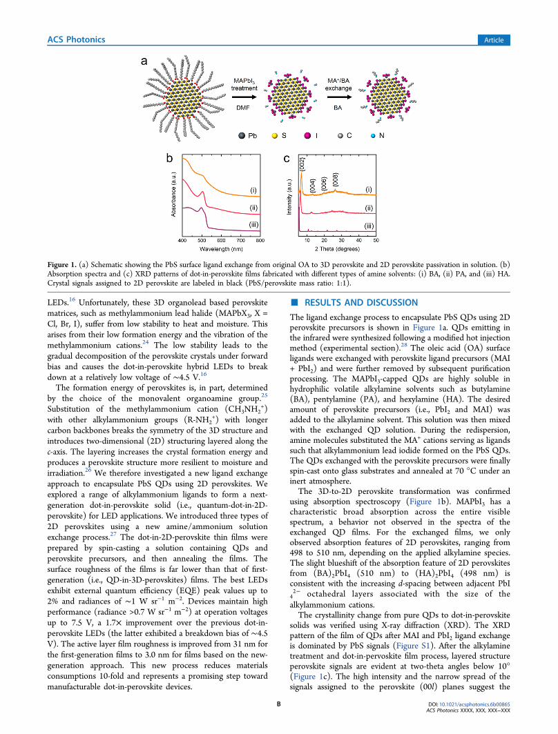
The ligand exchange process to encapsulate PbS QDs using 2Dperovskite precursors is shown in Figure 1a. QDs emitting inthe infrared were synthesized following a modified hot injectionmethod (experimental section).28 The oleic acid (OA) surfaceligands were exchanged with perovskite ligand precursors (MAI+ PbI2) and were further removed by subsequent purificationprocessing. The MAPbI3-capped QDs are highly soluble inhydrophilic volatile alkylamine solvents such as butylamine(BA), pentylamine (PA), and hexylamine (HA). The desiredamount of perovskite precursors (i.e., PbI2 and MAI) wasadded to the alkylamine solvent. This solution was then mixedwith the exchanged QD solution. During the redispersion,amine molecules substituted the MA+ cations serving as ligandssuch that alkylammonium lead iodide formed on the PbS QDs.The QDs exchanged with the perovskite precursors were finallyspin-cast onto glass substrates and annealed at 70 °C under aninert atmosphere.The 3D-to-2D perovskite transformation was confirmed
using absorption spectroscopy (Figure 1b). MAPbI3 has acharacteristic broad absorption across the entire visiblespectrum, a behavior not observed in the spectra of theexchanged QD films. For the exchanged films, we onlyobserved absorption features of 2D perovskites, ranging from498 to 510 nm, depending on the applied alkylamine species.The slight blueshift of the absorption feature of 2D perovskitesfrom (BA)2PbI4 (510 nm) to (HA)2PbI4 (498 nm) isconsistent with the increasing d-spacing between adjacent PbI42− octahedral layers associated with the size of thealkylammonium cations.The crystallinity change from pure QDs to dot-in-perovskite
solids was verified using X-ray diffraction (XRD). The XRDpattern of the film of QDs after MAI and PbI2 ligand exchangeis dominated by PbS signals (Figure S1). After the alkylaminetreatment and dot-in-pervoskite film process, layered structureperovskite signals are evident at two-theta angles below 10°(Figure 1c). The high intensity and the narrow spread of thesignals assigned to the perovskite (00l) planes suggest the
Figure 1. (a) Schematic showing the PbS surface ligand exchange from original OA to 3D perovskite and 2D perovskite passivation in solution. (b)Absorption spectra and (c) XRD patterns of dot-in-perovskite films fabricated with different types of amine solvents: (i) BA, (ii) PA, and (iii) HA.Crystal signals assigned to 2D perovskite are labeled in black (PbS/perovskite mass ratio: 1:1).
formation of large crystal domains. We also notice the shift ofthe {002} signals to lower angles as the length of thealkylammonium chains are increased: {002} signals at 6.7°,6.2°, and 5.4° for (BA)2PbI4, (PA)2PbI4, and (HA)2PbI4matrices, respectively. This trend is consistent with theexpansion of the unit cell of the 2D perovskite along the c-axis (c-axis lattice constant: (BA)2PbI4: 27.601 Å, (PA)2PbI4:14.881 Å (monoclinic) and 29.956 Å (orthorhombic),(HA)2PbI4: 32.703 Å).29 PbS QD features at ∼25° and ∼32°,which correspond to {111} and {200} lattice planes, arerelatively weak due to dilution by the perovskite and only canbe found when high concentration of QDs are present in thedot-in-perovskite film (Figure S2). The volatility of the aminesource is key to the formation of the 2D perovskite matrix:alkylamines with carbon numbers below four (e.g., propyl-amine) are too volatile to yield a crystallized and uniform QD-perovskite film from the postspin-casting process.Transmission electron microscope (TEM) imaging gives
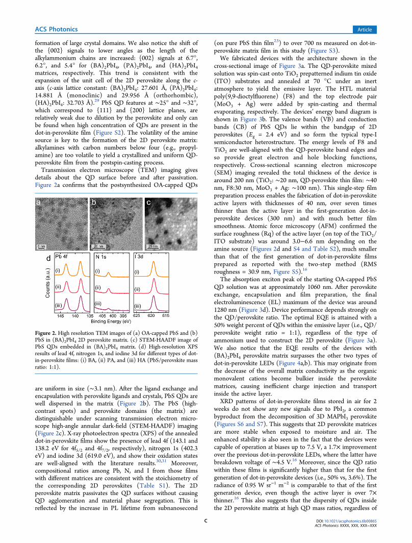
details about the QD surface before and after passivation.Figure 2a confirms that the postsynthesized OA-capped QDs
are uniform in size (∼3.1 nm). After the ligand exchange andencapsulation with perovskite ligands and crystals, PbS QDs arewell dispersed in the matrix (Figure 2b). The PbS (high-contrast spots) and perovskite domains (the matrix) aredistinguishable under scanning transmission electron micro-scope high-angle annular dark-field (STEM-HAADF) imaging(Figure 2c). X-ray photoelectron spectra (XPS) of the annealeddot-in-perovskite films show the presence of lead 4f (143.1 and138.2 eV for 4f5/2 and 4f7/2, respectively), nitrogen 1s (402.3eV) and iodine 3d (619.0 eV), and show their oxidation statesare well-aligned with the literature results.30,31 Moreover,compositional ratios among Pb, N, and I from those filmswith different matrices are consistent with the stoichiometry ofthe corresponding 2D perovskites (Table S1). The 2Dperovskite matrix passivates the QD surfaces without causingQD agglomeration and material phase segregation. This isreflected by the increase in PL lifetime from subnanosecond
(on pure PbS thin film23) to over 700 ns measured on dot-in-perovskite matrix film in this study (Figure S3).We fabricated devices with the architecture shown in the
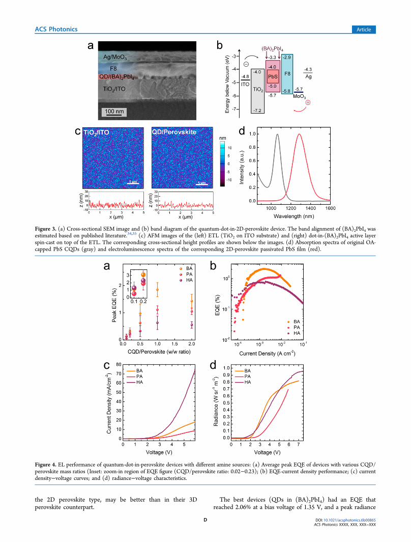
cross-sectional image of Figure 3a. The QD-perovskite mixedsolution was spin-cast onto TiO2 prepatterned indium tin oxide(ITO) substrates and annealed at 70 °C under an inertatmosphere to yield the emissive layer. The HTL materialpoly(9,9-dioctylfluorene) (F8) and the top electrode pair(MoO3 + Ag) were added by spin-casting and thermalevaporating, respectively. The devices’ energy band diagram isshown in Figure 3b. The valence bands (VB) and conductionbands (CB) of PbS QDs lie within the bandgap of 2Dperovskites (Eg = 2.4 eV) and so form the typical type-Isemiconductor heterostructure. The energy levels of F8 andTiO2 are well-aligned with the QD-perovskite band edges andso provide great electron and hole blocking functions,respectively. Cross-sectional scanning electron microscope(SEM) imaging revealed the total thickness of the device isaround 200 nm (TiO2: ∼20 nm, QD-perovskite thin film: ∼40nm, F8:30 nm, MoO3 + Ag: ∼100 nm). This single-step filmpreparation process enables the fabrication of dot-in-perovskiteactive layers with thicknesses of 40 nm, over seven timesthinner than the active layer in the first-generation dot-in-perovskite devices (300 nm) and with much better filmsmoothness. Atomic force microscopy (AFM) confirmed thesurface roughness (Rq) of the active layer (on top of the TiO2/ITO substrate) was around 3.0−6.6 nm depending on theamine source (Figures 2d and S4 and Table S2), much smallerthan that of the first generation of dot-in-perovskite filmsprepared as reported with the two-step method (RMSroughness = 30.9 nm, Figure S5).16
The absorption exciton peak of the starting OA-capped PbSQD solution was at approximately 1060 nm. After perovskiteexchange, encapsulation and film preparation, the finalelectroluminescence (EL) maximum of the device was around1280 nm (Figure 3d). Device performance depends strongly onthe QD/perovskite ratio. The optimal EQE is attained with a50% weight percent of QDs within the emissive layer (i.e., QD/perovskite weight ratio = 1:1), regardless of the type ofammonium used to construct the 2D perovskite (Figure 3a).We also notice that the EQE results of the devices with(BA)2PbI4 perovskite matrix surpasses the other two types ofdot-in-perovskite LEDs (Figure 4a,b). This may originate fromthe decrease of the overall matrix conductivity as the organicmonovalent cations become bulkier inside the perovskitematrices, causing inefficient charge injection and transportinside the active layer.XRD patterns of dot-in-perovskite films stored in air for 2
weeks do not show any new signals due to PbI2, a commonbyproduct from the decomposition of 3D MAPbI3 perovskite(Figures S6 and S7). This suggests that 2D perovskite matricesare more stable when exposed to moisture and air. Theenhanced stability is also seen in the fact that the devices werecapable of operation at biases up to 7.5 V, a 1.7× improvementover the previous dot-in-perovskite LEDs, where the latter havebreakdown voltage of ∼4.5 V.16 Moreover, since the QD ratiowithin these films is significantly higher than that for the firstgeneration of dot-in-perovskite devices (i.e., 50% vs, 3.6%). Theradiance of 0.95 W sr−1 m−2 is comparable to that of the firstgeneration device, even though the active layer is over 7×thinner.16 This also suggests that the dispersity of QDs insidethe 2D perovskite matrix at high QD mass ratios, regardless of
Figure 2. High resolution TEM images of (a) OA-capped PbS and (b)PbS in (BA)2PbI4 2D perovskite matrix. (c) STEM-HAADF image ofPbS QDs embedded in (BA)2PbI4 matrix. (d) High-resolution XPSresults of lead 4f, nitrogen 1s, and iodine 3d for different types of dot-in-perovskite films: (i) BA, (ii) PA, and (iii) HA (PbS/perovskite massratio: 1:1).
the 2D perovskite type, may be better than in their 3Dperovskite counterpart.
The best devices (QDs in (BA)2PbI4) had an EQE thatreached 2.06% at a bias voltage of 1.35 V, and a peak radiance
Figure 3. (a) Cross-sectional SEM image and (b) band diagram of the quantum-dot-in-2D-perovskite device. The band alignment of (BA)2PbI4 wasestimated based on published literature.34,35 (c) AFM images of the (left) ETL (TiO2 on ITO substrate) and (right) dot-in-(BA)2PbI4 active layerspin-cast on top of the ETL. The corresponding cross-sectional height profiles are shown below the images. (d) Absorption spectra of original OA-capped PbS CQDs (gray) and electroluminescence spectra of the corresponding 2D-perovskite passivated PbS film (red).
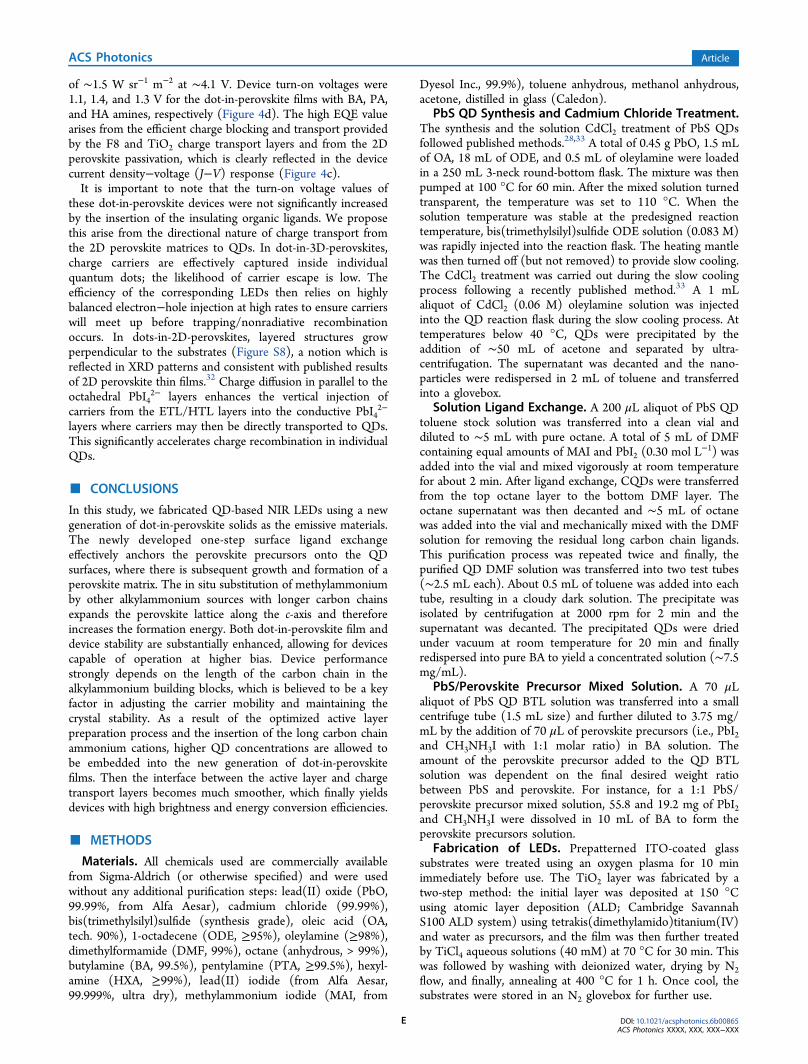
Figure 4. EL performance of quantum-dot-in-perovskite devices with different amine sources: (a) Average peak EQE of devices with various CQD/perovskite mass ratios (Inset: zoom-in region of EQE figure (CQD/perovskite ratio: 0.02−0.23); (b) EQE-current density performance; (c) currentdensity−voltage curves; and (d) radiance−voltage characteristics.
of ∼1.5 W sr−1 m−2 at ∼4.1 V. Device turn-on voltages were1.1, 1.4, and 1.3 V for the dot-in-perovskite films with BA, PA,and HA amines, respectively (Figure 4d). The high EQE valuearises from the efficient charge blocking and transport providedby the F8 and TiO2 charge transport layers and from the 2Dperovskite passivation, which is clearly reflected in the devicecurrent density−voltage (J−V) response (Figure 4c).It is important to note that the turn-on voltage values of
these dot-in-perovskite devices were not significantly increasedby the insertion of the insulating organic ligands. We proposethis arise from the directional nature of charge transport fromthe 2D perovskite matrices to QDs. In dot-in-3D-perovskites,charge carriers are effectively captured inside individualquantum dots; the likelihood of carrier escape is low. Theefficiency of the corresponding LEDs then relies on highlybalanced electron−hole injection at high rates to ensure carrierswill meet up before trapping/nonradiative recombinationoccurs. In dots-in-2D-perovskites, layered structures growperpendicular to the substrates (Figure S8), a notion which isreflected in XRD patterns and consistent with published resultsof 2D perovskite thin films.32 Charge diffusion in parallel to theoctahedral PbI4
2− layers enhances the vertical injection ofcarriers from the ETL/HTL layers into the conductive PbI4
2−
layers where carriers may then be directly transported to QDs.This significantly accelerates charge recombination in individualQDs.
■ CONCLUSIONS
In this study, we fabricated QD-based NIR LEDs using a newgeneration of dot-in-perovskite solids as the emissive materials.The newly developed one-step surface ligand exchangeeffectively anchors the perovskite precursors onto the QDsurfaces, where there is subsequent growth and formation of aperovskite matrix. The in situ substitution of methylammoniumby other alkylammonium sources with longer carbon chainsexpands the perovskite lattice along the c-axis and thereforeincreases the formation energy. Both dot-in-perovskite film anddevice stability are substantially enhanced, allowing for devicescapable of operation at higher bias. Device performancestrongly depends on the length of the carbon chain in thealkylammonium building blocks, which is believed to be a keyfactor in adjusting the carrier mobility and maintaining thecrystal stability. As a result of the optimized active layerpreparation process and the insertion of the long carbon chainammonium cations, higher QD concentrations are allowed tobe embedded into the new generation of dot-in-perovskitefilms. Then the interface between the active layer and chargetransport layers becomes much smoother, which finally yieldsdevices with high brightness and energy conversion efficiencies.
■ METHODS
Materials. All chemicals used are commercially availablefrom Sigma-Aldrich (or otherwise specified) and were usedwithout any additional purification steps: lead(II) oxide (PbO,99.99%, from Alfa Aesar), cadmium chloride (99.99%),bis(trimethylsilyl)sulfide (synthesis grade), oleic acid (OA,tech. 90%), 1-octadecene (ODE, ≥95%), oleylamine (≥98%),dimethylformamide (DMF, 99%), octane (anhydrous, > 99%),butylamine (BA, 99.5%), pentylamine (PTA, ≥99.5%), hexyl-amine (HXA, ≥99%), lead(II) iodide (from Alfa Aesar,99.999%, ultra dry), methylammonium iodide (MAI, from
PbS QD Synthesis and Cadmium Chloride Treatment.The synthesis and the solution CdCl2 treatment of PbS QDsfollowed published methods.28,33 A total of 0.45 g PbO, 1.5 mLof OA, 18 mL of ODE, and 0.5 mL of oleylamine were loadedin a 250 mL 3-neck round-bottom flask. The mixture was thenpumped at 100 °C for 60 min. After the mixed solution turnedtransparent, the temperature was set to 110 °C. When thesolution temperature was stable at the predesigned reactiontemperature, bis(trimethylsilyl)sulfide ODE solution (0.083 M)was rapidly injected into the reaction flask. The heating mantlewas then turned off (but not removed) to provide slow cooling.The CdCl2 treatment was carried out during the slow coolingprocess following a recently published method.33 A 1 mLaliquot of CdCl2 (0.06 M) oleylamine solution was injectedinto the QD reaction flask during the slow cooling process. Attemperatures below 40 °C, QDs were precipitated by theaddition of ∼50 mL of acetone and separated by ultra-centrifugation. The supernatant was decanted and the nano-particles were redispersed in 2 mL of toluene and transferredinto a glovebox.
Solution Ligand Exchange. A 200 μL aliquot of PbS QDtoluene stock solution was transferred into a clean vial anddiluted to ∼5 mL with pure octane. A total of 5 mL of DMFcontaining equal amounts of MAI and PbI2 (0.30 mol L−1) wasadded into the vial and mixed vigorously at room temperaturefor about 2 min. After ligand exchange, CQDs were transferredfrom the top octane layer to the bottom DMF layer. Theoctane supernatant was then decanted and ∼5 mL of octanewas added into the vial and mechanically mixed with the DMFsolution for removing the residual long carbon chain ligands.This purification process was repeated twice and finally, thepurified QD DMF solution was transferred into two test tubes(∼2.5 mL each). About 0.5 mL of toluene was added into eachtube, resulting in a cloudy dark solution. The precipitate wasisolated by centrifugation at 2000 rpm for 2 min and thesupernatant was decanted. The precipitated QDs were driedunder vacuum at room temperature for 20 min and finallyredispersed into pure BA to yield a concentrated solution (∼7.5mg/mL).
PbS/Perovskite Precursor Mixed Solution. A 70 μLaliquot of PbS QD BTL solution was transferred into a smallcentrifuge tube (1.5 mL size) and further diluted to 3.75 mg/mL by the addition of 70 μL of perovskite precursors (i.e., PbI2and CH3NH3I with 1:1 molar ratio) in BA solution. Theamount of the perovskite precursor added to the QD BTLsolution was dependent on the final desired weight ratiobetween PbS and perovskite. For instance, for a 1:1 PbS/perovskite precursor mixed solution, 55.8 and 19.2 mg of PbI2and CH3NH3I were dissolved in 10 mL of BA to form theperovskite precursors solution.
Fabrication of LEDs. Prepatterned ITO-coated glasssubstrates were treated using an oxygen plasma for 10 minimmediately before use. The TiO2 layer was fabricated by atwo-step method: the initial layer was deposited at 150 °Cusing atomic layer deposition (ALD; Cambridge SavannahS100 ALD system) using tetrakis(dimethylamido)titanium(IV)and water as precursors, and the film was then further treatedby TiCl4 aqueous solutions (40 mM) at 70 °C for 30 min. Thiswas followed by washing with deionized water, drying by N2flow, and finally, annealing at 400 °C for 1 h. Once cool, thesubstrates were stored in an N2 glovebox for further use.
The PbS-perovskite precursor mixed solutions were spin-coated (6000 rpm, 30 s) onto the TiO2 substrates and thenannealed at 70 °C for 10 min in an N2 glovebox to removebutylamine completely from the films. The F8/chlorobenzenesolution (10 mg mL−1) was annealed at 90 °C under nitrogenatmosphere and spin-cast onto the QD-in-perovskite layer at 70°C and 3000 rpm for 60 s to form a uniform hole transportlayer. The top electrode, consisting of 6 nm of MoO3 and 100nm of Ag, was deposited by thermal evaporation at a pressure<1 × 10⁻⁶ Torr. Each ITO substrate (2.5 cm × 2.5 cm) waspatterned to yield eight devices, each with an area of 3.1 mm2.PL and EL Measurements. PL measurements were
performed using a Horiba Fluorolog time-correlated single-photon counting system with photomultiplier tube detectors.The radiated power of EL was measured using a calibratedOphir PD300-IR germanium photodiode (active area: 19.6mm2) and recorded in situ using a computer-controlledKeithley 2,400 source meter under a nitrogen atmosphereand in parallel with the J−V measurements.Time-Resolved Photoluminescence Spectroscopy.
Time-resolved photoluminescence spectroscopy measurementswere performed using the Horiba Fluorolog Time-CorrelatedSingle Photon Counting (TCSPC) system equipped with UV/vis/NIR photomultiplier tube detectors, dual grating spec-trometers, and a monochromatized xenon lamp excitationsource. The film was placed at an incident angle of 30° awayfrom the detector to avoid reflections of the incident beam. A504 nm laser diode was used as a pulsed excitation source, andthe time traces were acquired using the TCSPC near-infrareddetector. The time window was set appropriately to ensure acomplete decay of the photogenerated carriers.Absorption and XRD Measurements. Optical absorption
measurements were carried out in a Lambda 950500 UV−vis-IR spectrophotometer. Powder XRD patterns were collectedusing a Rigaku MiniFlex 600 diffractometer equipped with aNaI scintillation counter and a monochromatized Copper Kαradiation source (λ = 1.5406 Å).Device Performance Characterization. Lambertian
emission was assumed in the calculation of EQE and radiance.Peak EQE was determined as the number of forward-emittedphotons to the number of injected electrons. A geometriccorrection factor was used according to the distance betweenthe photodiode and device and the active area of the detector.PCE was calculated as the radiative EL power divided by thetotal input electrical power.SEM, XPS, and AFM Measurements. SEM character-
ization was done on a Hitachi S-5200 scanning electronmicroscope. XPS analysis was carried out using ThermoScientific K-Alpha XPS system with an Ar ion gun. AFM wasdone with an Asylum Research Cypher system. The AFM wasoperated in AC mode in air to obtain topographical and phaseimages. Silicon ASYELEC-01 probes with titanium−iridiumcoatings from Asylum Research were used for all imaging.Probes typically have a spring constant of 2 N/m.TEM Measurement. High-resolution TEM and STEM-
HAADF images were obtained using the Hitachi S-5200microscope with an accelerating voltage of 300 kV. The TEMimages were processed using NIH ImageJ software (version:32-bit Java 1.6.0_24).TEM Sample Preparation. The above-mentioned 1:1 PbS
QD/perovskite precursor alkylamine solution was diluted fivetimes by adding additional clean alkylamine. Inside a nitrogen-filled glovebox, ∼25 μL of the precursor solution was drop-cast
onto a piece of carbon coated copper TEM grid (300 mesh,Ted Pella, Inc., 01824G) and further annealed at 70 °C for 10min under nitrogen atmosphere. When it was cooled down toroom temperature, the sample grid was stored in a TEM sampleholder inside the nitrogen-filled glovebox.
■ ASSOCIATED CONTENT*S Supporting InformationThe Supporting Information is available free of charge on theACS Publications website at DOI: 10.1021/acsphoto-nics.6b00865.
AFM results of the quantum-dot-in-perovskite activelayer with PA and HA amines and the quantum-dot-in-perovskite film prepared following ref 16, and a table thatshows XPS data regarding about elemental compositionand the ratio of active materials with various aminesources (PDF).
■ ACKNOWLEDGMENTSThis publication is based in part on work supported by AwardKUS-11-009-21, from King Abdullah University of Science andTechnology (KAUST), by the Ontario Research Fund -Research Excellence Program, and by the Natural Sciencesand Engineering Research Council of Canada (NSERC). E.Yassitepe and P. Kanjanaboos are thanked for the assistance ofHRTEM, STEM, and AFM measurements. The authors thankL. Gao, R. Wolowiec, D. Kopilovic, and E. Palmiano for theirhelp and useful discussions.
■ REFERENCES(1) Efros, A. L. Interband absorption of light in a semiconductorsphere. Soviet Physics Semiconductors-Ussr 1982, 16, 772−775.(2) Rossetti, R.; Nakahara, S.; Brus, L. E. Quantum size effects in theredox potentials, resonance Raman spectra, and electronic spectra ofCdS crystallites in aqueous solution. J. Chem. Phys. 1983, 79, 1086−1088.(3) Colvin, V. L.; Schlamp, M. C.; Alivisatos, A. P. Light-emittingdiodes made from cadmium selenide nanocrystals and a semi-conducting polymer. Nature 1994, 370, 354−357.(4) Dabbousi, B. O.; Bawendi, M. G.; Onitsuka, O.; Rubner, M. F.Electroluminescence from CdSe quantum-dot/polymer composites.Appl. Phys. Lett. 1995, 66, 1316−1318.(5) Coe, S.; Woo, W.-K.; Bawendi, M.; Bulovic, V. Electro-luminescence from single monolayers of nanocrystals in molecularorganic devices. Nature 2002, 420, 800−803.(6) Tessler, N.; Medvedev, V.; Kazes, M.; Kan, S.; Banin, U. EfficientNear-Infrared Polymer Nanocrystal Light-Emitting Diodes. Science2002, 295, 1506−1508.(7) Sargent, E. H. Infrared Quantum Dots. Adv. Mater. 2005, 17,515−522.(8) Anikeeva, P. O.; Halpert, J. E.; Bawendi, M. G.; Bulovic,́ V.Quantum Dot Light-Emitting Devices with ElectroluminescenceTunable over the Entire Visible Spectrum. Nano Lett. 2009, 9,2532−2536.
(9) Shirasaki, Y.; Supran, G. J.; Bawendi, M. G.; Bulovic, V.Emergence of colloidal quantum-dot light-emitting technologies. Nat.Photonics 2012, 7, 13−23.(10) Bourdakos, K. N.; Dissanayake, D. M. N. M.; Lutz, T.; Silva, S.R. P.; Curry, R. J. Highly efficient near-infrared hybrid organic-inorganic nanocrystal electroluminescence device. Appl. Phys. Lett.2008, 92, 153311.(11) Choudhury, K. R.; Song, D. W.; So, F. Efficient solution-processed hybrid polymer−nanocrystal near infrared light-emittingdevices. Org. Electron. 2010, 11, 23−28.(12) Ma, X.; Xu, F.; Benavides, J.; Cloutier, S. G. High performancehybrid near-infrared LEDs using benzenedithiol cross-linked PbScolloidal nanocrystals. Org. Electron. 2012, 13, 525−531.(13) Sun, L.; Choi, J. J.; Stachnik, D.; Bartnik, A. C.; Hyun, B.-R.;Malliaras, G. G.; Hanrath, T.; Wise, F. W. Bright infrared quantum-dotlight-emitting diodes through inter-dot spacing control. Nat. Nano-technol. 2012, 7, 369−373.(14) Supran, G. J.; Song, K. W.; Hwang, G. W.; Correa, R. E.;Scherer, J.; Dauler, E. A.; Shirasaki, Y.; Bawendi, M. G.; Bulovic,́ V.High-Performance Shortwave-Infrared Light-Emitting Devices UsingCore−Shell (PbS−CdS) Colloidal Quantum Dots. Adv. Mater. 2015,27, 1437−1442.(15) Krames, M. R.; Shchekin, O. B.; Mueller-Mach, R.; Mueller, G.O.; Zhou, L.; Harbers, G.; Craford, M. G. Status and Future of High-Power Light-Emitting Diodes for Solid-State Lighting. J. Disp. Technol.2007, 3, 160−175.(16) Gong, X.; Yang, Z.; Walters, G.; Comin, R.; Ning, Z.;Beauregard, E.; Adinolfi, V.; Voznyy, O.; Sargent, E. H. Highlyefficient quantum dot near-infrared light-emitting diodes. Nat.Photonics 2016, 10, 253−257.(17) Semonin, O. E.; Johnson, J. C.; Luther, J. M.; Midgett, A. G.;Nozik, A. J.; Beard, M. C. Absolute Photoluminescence QuantumYields of IR-26 Dye, PbS, and PbSe Quantum Dots. J. Phys. Chem. Lett.2010, 1, 2445−2450.(18) Zhitomirsky, D.; Voznyy, O.; Hoogland, S.; Sargent, E. H.Measuring charge carrier diffusion in coupled colloidal quantum dotsolids. ACS Nano 2013, 7, 5282−5290.(19) Choi, J. J.; Luria, J.; Hyun, B.-R.; Bartnik, A. C.; Sun, L.; Lim, Y.-F.; Marohn, J. A.; Wise, F. W.; Hanrath, T. Photogenerated ExcitonDissociation in Highly Coupled Lead Salt Nanocrystal Assemblies.Nano Lett. 2010, 10, 1805−1811.(20) Greenham, N. C.; Peng, X.; Alivisatos, A. P. Charge separationand transport in conjugated-polymer/semiconductor-nanocrystalcomposites studied by photoluminescence quenching and photo-conductivity. Phys. Rev. B: Condens. Matter Mater. Phys. 1996, 54,17628−17637.(21) Steckel, J. S.; Coe-Sullivan, S.; Bulovic,́ V.; Bawendi, M. G. 1.3 to1.55 μm Tunable Electroluminescence from PbSe Quantum DotsEmbedded within an Organic Device. Adv. Mater. 2003, 15, 1862−1866.(22) Moroz, P.; Liyanage, G.; Kholmicheva, N. N.; Yakunin, S.; Rijal,U.; Uprety, P.; Bastola, E.; Mellott, B.; Subedi, K.; Sun, L.; Kovalenko,M. V.; Zamkov, M. Infrared Emitting PbS Nanocrystal Solids throughMatrix Encapsulation. Chem. Mater. 2014, 26, 4256−4264.(23) Ning, Z.; Gong, X.; Comin, R.; Walters, G.; Fan, F.; Voznyy, O.;Yassitepe, E.; Buin, A.; Hoogland, S.; Sargent, E. H. Quantum-dot-in-perovskite solids. Nature 2015, 523, 324−328.(24) Buin, A.; Pietsch, P.; Xu, J.; Voznyy, O.; Ip, A. H.; Comin, R.;Sargent, E. H. Materials Processing Routes to Trap-Free HalidePerovskites. Nano Lett. 2014, 14, 6281−6286.(25) Saparov, B.; Mitzi, D. B. Organic−Inorganic Perovskites:Structural Versatility for Functional Materials Design. Chem. Rev.2016, 116, 4558−4596.(26) Quan, L. N.; Yuan, M.; Comin, R.; Voznyy, O.; Beauregard, E.M.; Hoogland, S.; Buin, A.; Kirmani, A. R.; Zhao, K.; Amassian, A.;Kim, D. H.; Sargent, E. H. Ligand-Stabilized Reduced-DimensionalityPerovskites. J. Am. Chem. Soc. 2016, 138, 2649−2655.
(27) Yang, Z.; Yassitepe, E.; Voznyy, O.; Janmohamed, A.; Lan, X.;Levina, L.; Comin, R.; Sargent, E. H. Self-Assembled PbSe Nanowire:Perovskite Hybrids. J. Am. Chem. Soc. 2015, 137, 14869−14872.(28) Hines, M. A.; Scholes, G. D. Colloidal PbS Nanocrystals withSize-Tunable Near-Infrared Emission: Observation of Post-SynthesisSelf-Narrowing of the Particle Size Distribution. Adv. Mater. 2003, 15,1844−1849.(29) Billing, D. G.; Lemmerer, A. Synthesis, characterization andphase transitions in the inorganic-organic layered perovskite-typehybrids [(CnH2n + 1NH3)2PbI4], n = 4, 5 and 6. Acta Crystallogr.,Sect. B: Struct. Sci. 2007, 63, 735−747.(30) Calloni, A.; Abate, A.; Bussetti, G.; Berti, G.; Yivlialin, R.;Ciccacci, F.; Duo,̀ L. Stability of Organic Cations in Solution-Processed CH3NH3PbI3 Perovskites: Formation of Modified SurfaceLayers. J. Phys. Chem. C 2015, 119, 21329−21335.(31) Liu, L.; McLeod, J. A.; Wang, R.; Shen, P.; Duhm, S. Trackingthe formation of methylammonium lead triiodide perovskite. Appl.Phys. Lett. 2015, 107, 061904.(32) Cao, D. H.; Stoumpos, C. C.; Farha, O. K.; Hupp, J. T.;Kanatzidis, M. G. 2D Homologous Perovskites as Light-AbsorbingMaterials for Solar Cell Applications. J. Am. Chem. Soc. 2015, 137,7843−7850.(33) Yang, Z.; Voznyy, O.; Liu, M.; Yuan, M.; Ip, A. H.; Ahmed, O.S.; Levina, L.; Kinge, S.; Hoogland, S.; Sargent, E. H. All-Quantum-Dot Infrared Light-Emitting Diodes. ACS Nano 2015, 9, 12327−12333.(34) Comin, R.; Walters, G.; Thibau, E. S.; Voznyy, O.; Lu, Z.-H.;Sargent, E. H. Structural, optical, and electronic studies of wide-bandgap lead halide perovskites. J. Mater. Chem. C 2015, 3, 8839−8843.(35) Safdari, M.; Svensson, P. H.; Hoang, M. T.; Oh, I.; Kloo, L.;Gardner, J. M. Layered 2D alkyldiammonium lead iodide perovskites:synthesis, characterization, and use in solar cells. J. Mater. Chem. A2016, 4, 15638−15646.