Quartus II Introduction Using Schematic Designs For Quartus II 13.0 1 Introduction This tutorial presents an introduction to the Quartus ® II CAD system. It gives a general overview of a typical CAD flow for designing circuits that are implemented by using FPGA devices, and shows how this flow is realized in the Quartus II software. The design process is illustrated by giving step-by-step instructions for using the Quartus II software to implement a very simple circuit in an Altera FPGA device. The Quartus II system includes full support for all of the popular methods of entering a description of the desired circuit into a CAD system. This tutorial makes use of the schematic design entry method, in which the user draws a graphical diagram of the circuit. Two other versions of this tutorial are also available, which use the Verilog and VHDL hardware description languages, respectively. The last step in the design process involves configuring the designed circuit in an actual FPGA device. To show how this is done, it is assumed that the user has access to the Altera DE-series Development and Education board connected to a computer that has Quartus II software installed. A reader who does not have access to the DE-series board will still find the tutorial useful to learn how the FPGA programming and configuration task is performed. The screen captures in the tutorial were obtained using the Quartus II version 13.0; if other versions of the software are used, some of the images may be slightly different. Contents: • Typical CAD Flow • Getting Started • Starting a New Project • Schematic Design Entry • Compiling the Design • Pin Assignment • Simulating the Designed Circuit • Programming and Configuring the FPGA Device • Testing the Designed Circuit Altera Corporation - University Program May 2013 1
Transcript
Quartus II IntroductionUsing Schematic Designs
For Quartus II 13.0
1 Introduction
This tutorial presents an introduction to the Quartus® II CAD system. It gives a general overview of a typical CADflow for designing circuits that are implemented by using FPGA devices, and shows how this flow is realized in theQuartus II software. The design process is illustrated by giving step-by-step instructions for using the Quartus IIsoftware to implement a very simple circuit in an Altera FPGA device.
The Quartus II system includes full support for all of the popular methods of entering a description of the desiredcircuit into a CAD system. This tutorial makes use of the schematic design entry method, in which the user drawsa graphical diagram of the circuit. Two other versions of this tutorial are also available, which use the Verilog andVHDL hardware description languages, respectively.
The last step in the design process involves configuring the designed circuit in an actual FPGA device. To showhow this is done, it is assumed that the user has access to the Altera DE-series Development and Education boardconnected to a computer that has Quartus II software installed. A reader who does not have access to the DE-seriesboard will still find the tutorial useful to learn how the FPGA programming and configuration task is performed.
The screen captures in the tutorial were obtained using the Quartus II version 13.0; if other versions of the softwareare used, some of the images may be slightly different.
QUARTUS II INTRODUCTION USING SCHEMATIC DESIGNS For Quartus II 13.0
2 Background
Computer Aided Design (CAD) software makes it easy to implement a desired logic circuit by using a programmablelogic device, such as a field-programmable gate array (FPGA) chip. A typical FPGA CAD flow is illustrated inFigure 1.
Figure 1. Typical CAD flow.
The CAD flow involves the following steps:
• Design Entry – the desired circuit is specified either by means of a schematic diagram, or by using a hardwaredescription language, such as Verilog or VHDL
• Synthesis – the entered design is synthesized into a circuit that consists of the logic elements (LEs) providedin the FPGA chip
• Functional Simulation – the synthesized circuit is tested to verify its functional correctness; this simulationdoes not take into account any timing issues
QUARTUS II INTRODUCTION USING SCHEMATIC DESIGNS For Quartus II 13.0
• Fitting – the CAD Fitter tool determines the placement of the LEs defined in the netlist into the LEs in anactual FPGA chip; it also chooses routing wires in the chip to make the required connections between specificLEs
• Timing Analysis – propagation delays along the various paths in the fitted circuit are analyzed to provide anindication of the expected performance of the circuit
• Timing Simulation – the fitted circuit is tested to verify both its functional correctness and timing
• Programming and Configuration – the designed circuit is implemented in a physical FPGA chip by pro-gramming the configuration switches that configure the LEs and establish the required wiring connections
This tutorial introduces the basic features of the Quartus II software. It shows how the software can be used to designand implement a circuit specified by means of a schematic diagram. It makes use of the graphical user interface toinvoke the Quartus II commands. Doing this tutorial, the reader will learn about:
• Creating a project
• Entering a schematic diagram
• Synthesizing a circuit from the schematic diagram
• Fitting a synthesized circuit into an Altera FPGA
• Assigning the circuit inputs and outputs to specific pins on the FPGA
• Simulating the designed circuit
• Programming and configuring the FPGA chip on Altera’s DE-series board
3 Getting Started
Each logic circuit, or subcircuit, being designed with Quartus II software is called a project. The software works onone project at a time and keeps all information for that project in a single directory (folder) in the file system. Tobegin a new logic circuit design, the first step is to create a directory to hold its files. To hold the design files for thistutorial, we will use a directory introtutorial. The running example for this tutorial is a simple circuit for two-waylight control.
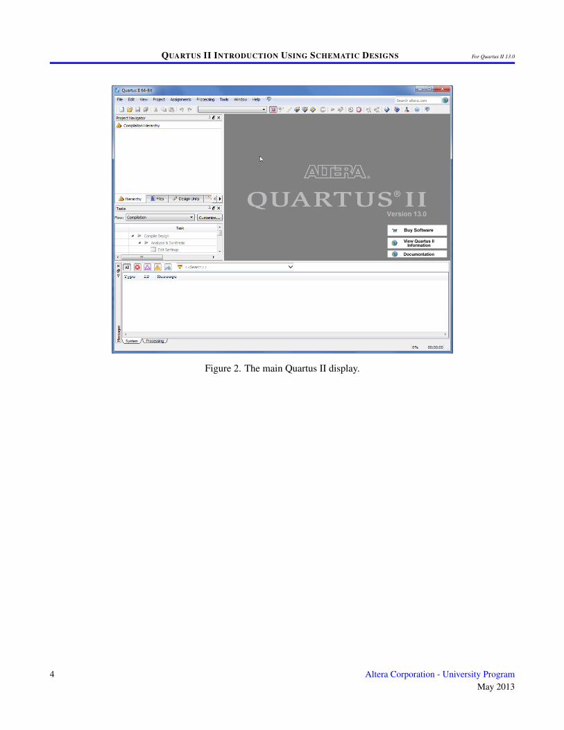
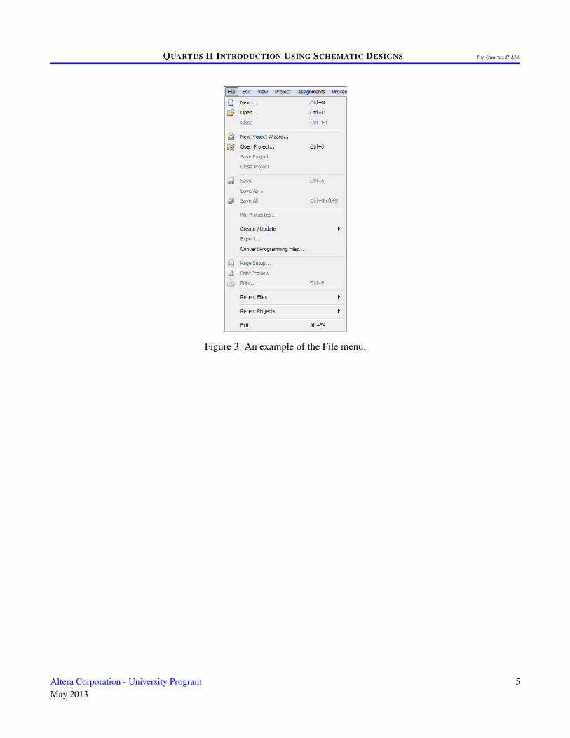
Start the Quartus II software. You should see a display similar to the one in Figure 2. This display consists of severalwindows that provide access to all the features of Quartus II software, which the user selects with the computermouse. Most of the commands provided by Quartus II software can be accessed by using a set of menus that arelocated below the title bar. For example, in Figure 2 clicking the left mouse button on the menu named File opens themenu shown in Figure 3. Clicking the left mouse button on the entry Exit exits from Quartus II software. In general,whenever the mouse is used to select something, the left button is used. Hence we will not normally specify whichbutton to press. In the few cases when it is necessary to use the right mouse button, it will be specified explicitly.
QUARTUS II INTRODUCTION USING SCHEMATIC DESIGNS For Quartus II 13.0
For some commands it is necessary to access two or more menus in sequence. We use the convention Menu1 >Menu2 > Item to indicate that to select the desired command the user should first click the left mouse button onMenu1, then within this menu click on Menu2, and then within Menu2 click on Item. For example, File > Exituses the mouse to exit from the system. Many commands can be invoked by clicking on an icon displayed in one ofthe toolbars. To see the command associated with an icon, position the mouse over the icon and a tooltip will appearthat displays the command name.
3.1 Quartus II Online Help
Quartus II software provides comprehensive online documentation that answers many of the questions that may arisewhen using the software. The documentation is accessed from the Help menu. To get some idea of the extent ofdocumentation provided, it is worthwhile for the reader to browse through the Help menu.
If no web browser is specified, Quartus will complain with an error message. To specify a web browser, go to Tools> Options... > General > Internet Connectivity. Specify a path to a web browser in the web browser field.
The user can quickly search through the Help topics by selecting Help > Search, which opens a dialog box intowhich keywords can be entered. Another method, context-sensitive help, is provided for quickly finding documen-tation for specific topics. While using most applications, pressing the F1 function key on the keyboard opens a Helpdisplay that shows the commands available for the application.
4 Starting a New Project
To start working on a new design we first have to define a new design project. Quartus II software makes thedesigner’s task easy by providing support in the form of a wizard. Create a new project as follows:
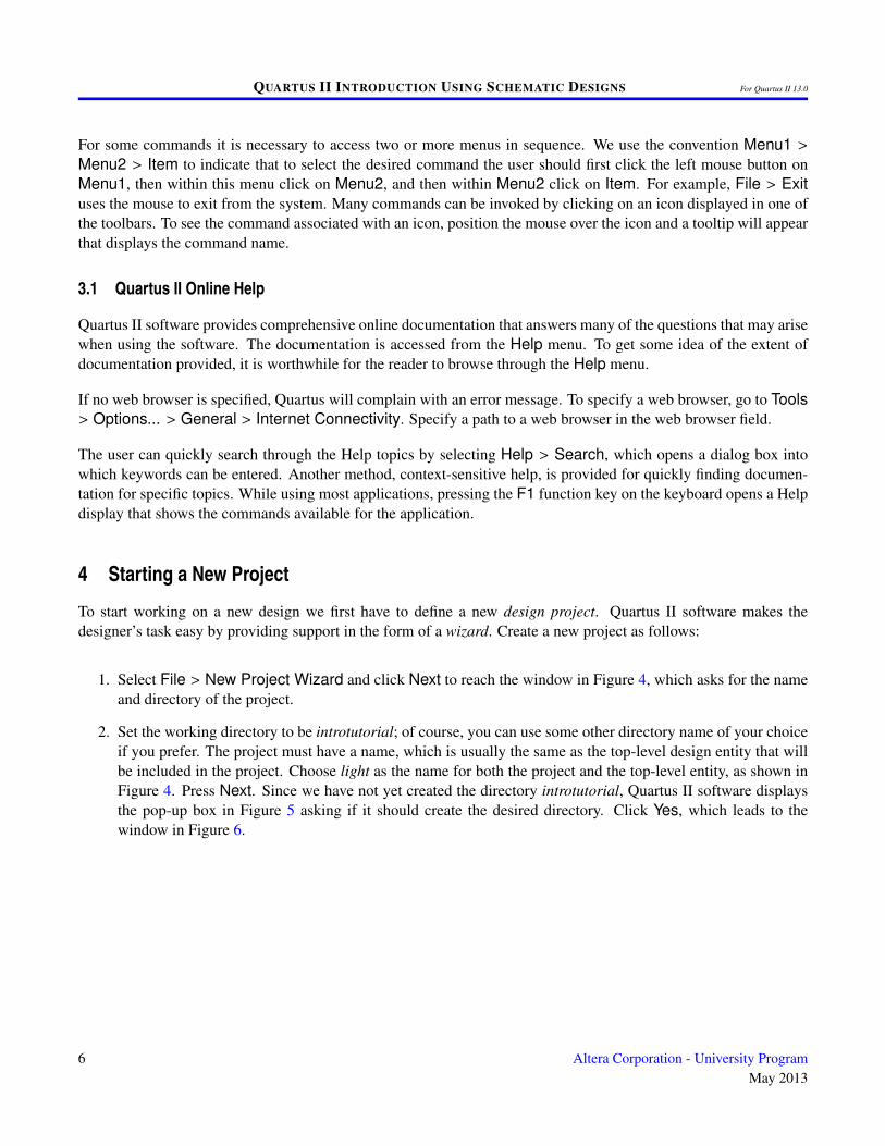
1. Select File > New Project Wizard and click Next to reach the window in Figure 4, which asks for the nameand directory of the project.
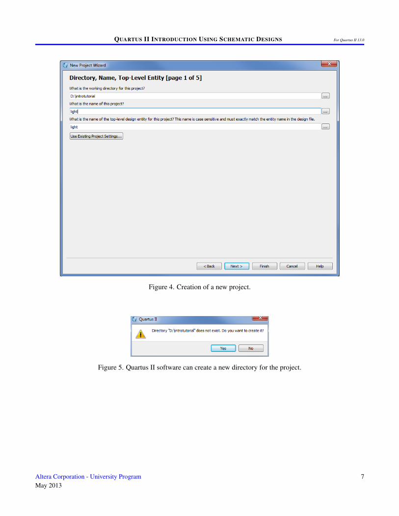
2. Set the working directory to be introtutorial; of course, you can use some other directory name of your choiceif you prefer. The project must have a name, which is usually the same as the top-level design entity that willbe included in the project. Choose light as the name for both the project and the top-level entity, as shown inFigure 4. Press Next. Since we have not yet created the directory introtutorial, Quartus II software displaysthe pop-up box in Figure 5 asking if it should create the desired directory. Click Yes, which leads to thewindow in Figure 6.
QUARTUS II INTRODUCTION USING SCHEMATIC DESIGNS For Quartus II 13.0
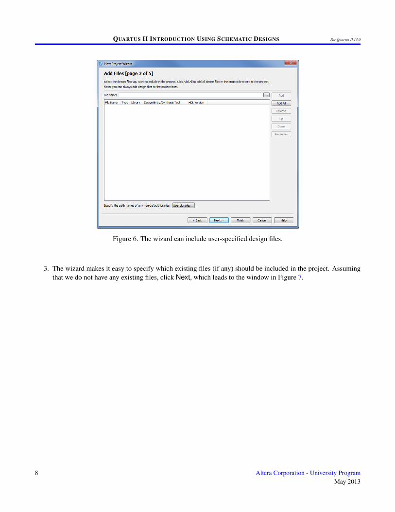
Figure 6. The wizard can include user-specified design files.
3. The wizard makes it easy to specify which existing files (if any) should be included in the project. Assumingthat we do not have any existing files, click Next, which leads to the window in Figure 7.
QUARTUS II INTRODUCTION USING SCHEMATIC DESIGNS For Quartus II 13.0
Figure 7. Choose the device family and a specific device.
4. We have to specify the type of device in which the designed circuit will be implemented. Choose the Cyclone-series device family for your DE-series board. We can let Quartus II software select a specific device in thefamily, or we can choose the device explicitly. We will take the latter approach. From the list of availabledevices, choose the appropriate device name for your DE-series board. A list of devices names on DE-seriesboards can be found in Table 1. Press Next, which opens the window in Figure 8.
Board Device NameDE0 Cyclone III EP3C16F484C6
DE0-Nano Cyclone IVE EP4CE22F17C6DE1 Cyclone II EP2C20F484C7DE2 Cyclone II EP2C35F672C6
DE2-70 Cyclone II EP2C70F896C6DE2-115 Cyclone IVE EP4CE115F29C7
QUARTUS II INTRODUCTION USING SCHEMATIC DESIGNS For Quartus II 13.0
Figure 8. Other EDA tools can be specified.
5. The user can specify any third-party tools that should be used. A commonly used term for CAD softwarefor electronic circuits is EDA tools, where the acronym stands for Electronic Design Automation. This termis used in Quartus II messages that refer to third-party tools, which are the tools developed and marketed bycompanies other than Altera. Since we will rely solely on Quartus II tools, we will not choose any other tools.Press Next.
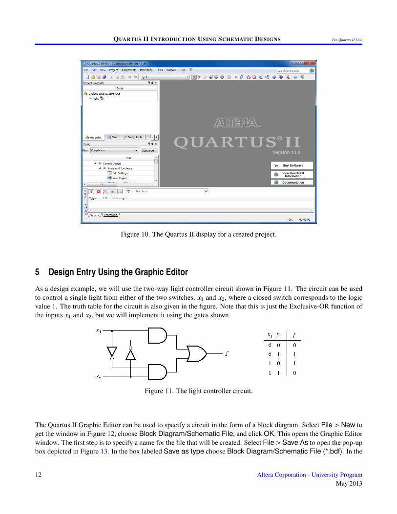
6. A summary of the chosen settings appears in the screen shown in Figure 9. Press Finish, which returns to themain Quartus II window, but with light specified as the new project, in the display title bar, as indicated inFigure 10.
10 Altera Corporation - University ProgramMay 2013
QUARTUS II INTRODUCTION USING SCHEMATIC DESIGNS For Quartus II 13.0
Figure 10. The Quartus II display for a created project.
5 Design Entry Using the Graphic Editor
As a design example, we will use the two-way light controller circuit shown in Figure 11. The circuit can be usedto control a single light from either of the two switches, x1 and x2, where a closed switch corresponds to the logicvalue 1. The truth table for the circuit is also given in the figure. Note that this is just the Exclusive-OR function ofthe inputs x1 and x2, but we will implement it using the gates shown.
Figure 11. The light controller circuit.
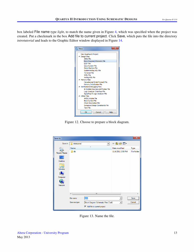
The Quartus II Graphic Editor can be used to specify a circuit in the form of a block diagram. Select File > New toget the window in Figure 12, choose Block Diagram/Schematic File, and click OK. This opens the Graphic Editorwindow. The first step is to specify a name for the file that will be created. Select File > Save As to open the pop-upbox depicted in Figure 13. In the box labeled Save as type choose Block Diagram/Schematic File (*.bdf). In the
12 Altera Corporation - University ProgramMay 2013
QUARTUS II INTRODUCTION USING SCHEMATIC DESIGNS For Quartus II 13.0
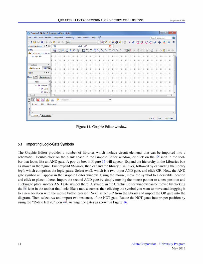
box labeled File name type light, to match the name given in Figure 4, which was specified when the project wascreated. Put a checkmark in the box Add file to current project. Click Save, which puts the file into the directoryintrotutorial and leads to the Graphic Editor window displayed in Figure 14.
QUARTUS II INTRODUCTION USING SCHEMATIC DESIGNS For Quartus II 13.0
Figure 14. Graphic Editor window.
5.1 Importing Logic-Gate Symbols
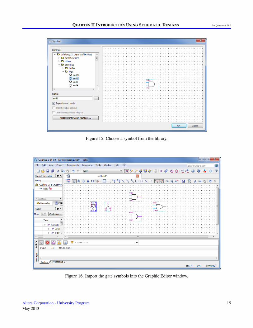
The Graphic Editor provides a number of libraries which include circuit elements that can be imported into aschematic. Double-click on the blank space in the Graphic Editor window, or click on the icon in the tool-bar that looks like an AND gate. A pop-up box in Figure 15 will appear. Expand the hierarchy in the Libraries boxas shown in the figure. First expand libraries, then expand the library primitives, followed by expanding the librarylogic which comprises the logic gates. Select and2, which is a two-input AND gate, and click OK. Now, the ANDgate symbol will appear in the Graphic Editor window. Using the mouse, move the symbol to a desirable locationand click to place it there. Import the second AND gate by simply moving the mouse pointer to a new position andclicking to place another AND gate symbol there. A symbol in the Graphic Editor window can be moved by clickingthe icon in the toolbar that looks like a mouse cursor, then clicking the symbol you want to move and dragging itto a new location with the mouse button pressed. Next, select or2 from the library and import the OR gate into thediagram. Then, select not and import two instances of the NOT gate. Rotate the NOT gates into proper position byusing the “Rotate left 90" icon . Arrange the gates as shown in Figure 16.
14 Altera Corporation - University ProgramMay 2013
QUARTUS II INTRODUCTION USING SCHEMATIC DESIGNS For Quartus II 13.0
5.2 Importing Input and Output Symbols
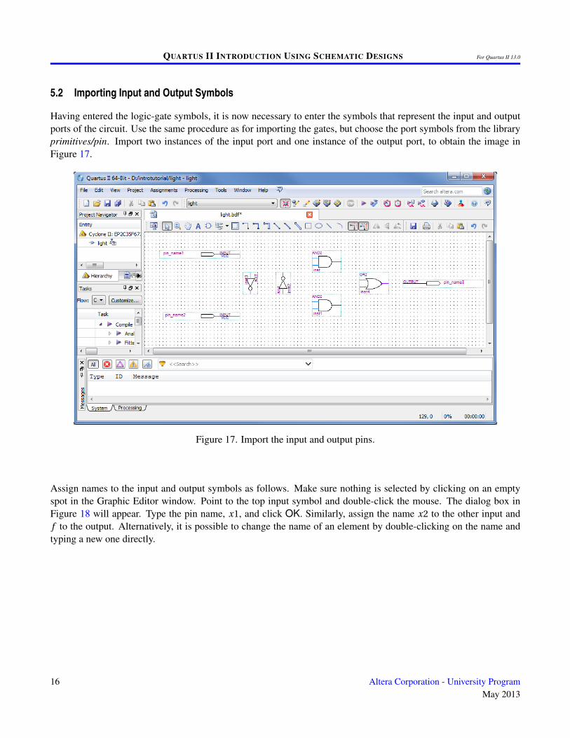
Having entered the logic-gate symbols, it is now necessary to enter the symbols that represent the input and outputports of the circuit. Use the same procedure as for importing the gates, but choose the port symbols from the libraryprimitives/pin. Import two instances of the input port and one instance of the output port, to obtain the image inFigure 17.
Figure 17. Import the input and output pins.
Assign names to the input and output symbols as follows. Make sure nothing is selected by clicking on an emptyspot in the Graphic Editor window. Point to the top input symbol and double-click the mouse. The dialog box inFigure 18 will appear. Type the pin name, x1, and click OK. Similarly, assign the name x2 to the other input andf to the output. Alternatively, it is possible to change the name of an element by double-clicking on the name andtyping a new one directly.
16 Altera Corporation - University ProgramMay 2013
QUARTUS II INTRODUCTION USING SCHEMATIC DESIGNS For Quartus II 13.0
Figure 18. Naming of a pin.
5.3 Connecting Nodes with Wires
The symbols in the diagram have to be connected by drawing lines (wires). Click on the icon in the toolbar toactivate the Orthogonal Node Tool. Position the mouse pointer over the right edge of the x1 input pin. Click andhold the mouse button and drag the mouse to the right until the drawn line reaches the pinstub on the top input of theAND gate. Release the mouse button when you see a box appear, which leaves the line connecting the two pinstubs.Next, draw a wire from the input pinstub of the leftmost NOT gate to touch the wire that was drawn above it. Notethat a dot will appear indicating a connection between the two wires.
Use the same procedure to draw the remaining wires in the circuit. If a mistake is made, a wire can be selected byclicking on it, and removed by pressing the Delete key on the keyboard. Upon completing the diagram, click on the
icon, to activate the Selection Tool. Now, changes in the appearance of the diagram can be made by selecting aparticular symbol or wire and either moving it to a different location or deleting it. The final diagram is shown inFigure 19; save it.
QUARTUS II INTRODUCTION USING SCHEMATIC DESIGNS For Quartus II 13.0
Figure 19. The completed schematic diagram.
6 Compiling the Designed Circuit
The entered schematic diagram file, light.bdf, is processed by several Quartus II tools that analyze the file, synthesizethe circuit, and generate an implementation of it for the target chip. These tools are controlled by the applicationprogram called the Compiler.
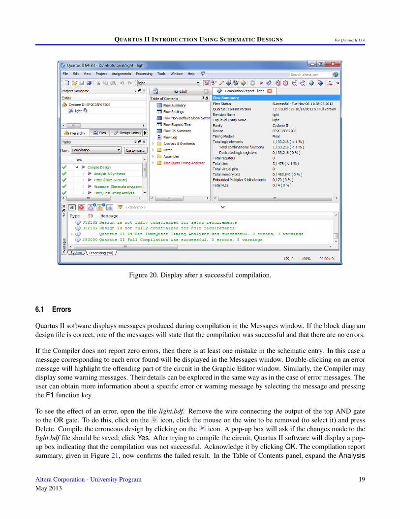
Run the Compiler by selecting Processing > Start Compilation, or by clicking on the toolbar icon that lookslike a purple triangle. Your project must be saved before compiling. As the compilation moves through variousstages, its progress is reported in a window on the left side of the Quartus II display. Successful (or unsuccessful)compilation is indicated in a pop-up box. Acknowledge it by clicking OK, which leads to the Quartus II display inFigure 20. In the message window, at the bottom of the figure, various messages are displayed. In case of errors,there will be appropriate messages given.
When the compilation is finished, a compilation report is produced. A tab showing this report is opened automat-ically, as seen in Figure 20. The tab can be closed in the normal way, and it can be opened at any time either byselecting Processing > Compilation Report or by clicking on the icon . The report includes a number of sec-tions listed on the left side. Figure 20 displays the Compiler Flow Summary section, which indicates that only onelogic element and three pins are needed to implement this tiny circuit on the selected FPGA chip.
18 Altera Corporation - University ProgramMay 2013
QUARTUS II INTRODUCTION USING SCHEMATIC DESIGNS For Quartus II 13.0
Figure 20. Display after a successful compilation.
6.1 Errors
Quartus II software displays messages produced during compilation in the Messages window. If the block diagramdesign file is correct, one of the messages will state that the compilation was successful and that there are no errors.
If the Compiler does not report zero errors, then there is at least one mistake in the schematic entry. In this case amessage corresponding to each error found will be displayed in the Messages window. Double-clicking on an errormessage will highlight the offending part of the circuit in the Graphic Editor window. Similarly, the Compiler maydisplay some warning messages. Their details can be explored in the same way as in the case of error messages. Theuser can obtain more information about a specific error or warning message by selecting the message and pressingthe F1 function key.
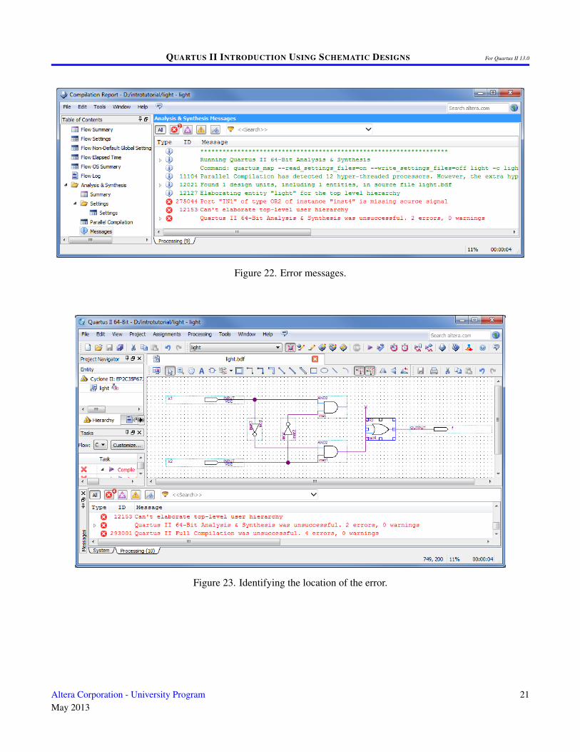
To see the effect of an error, open the file light.bdf. Remove the wire connecting the output of the top AND gateto the OR gate. To do this, click on the icon, click the mouse on the wire to be removed (to select it) and pressDelete. Compile the erroneous design by clicking on the icon. A pop-up box will ask if the changes made to thelight.bdf file should be saved; click Yes. After trying to compile the circuit, Quartus II software will display a pop-up box indicating that the compilation was not successful. Acknowledge it by clicking OK. The compilation reportsummary, given in Figure 21, now confirms the failed result. In the Table of Contents panel, expand the Analysis
QUARTUS II INTRODUCTION USING SCHEMATIC DESIGNS For Quartus II 13.0
& Synthesis part of the report and then select Messages to have the messages displayed as shown in Figure 22.The Compilation Report can be dispayed as a separate window as in Figure 22 by right-clicking its tab and selectingDetach Window, and can be reattached by clicking Window > Attatch Window. Double-click on the first errormessage, which states that one of the nodes is missing a source. Quartus II software responds by displaying thelight.bdf schematic and highlighting the OR gate which is affected by the error, as shown in Figure 23. Correct theerror and recompile the design.
Figure 21. Compilation report for the failed design.
20 Altera Corporation - University ProgramMay 2013
QUARTUS II INTRODUCTION USING SCHEMATIC DESIGNS For Quartus II 13.0
7 Pin Assignment
During the compilation above, the Quartus II Compiler was free to choose any pins on the selected FPGA to serve asinputs and outputs. However, the DE-series board has hardwired connections between the FPGA pins and the othercomponents on the board. We will use two toggle switches, labeled SW0 and SW1, to provide the external inputs, x1
and x2, to our example circuit. These switches are connected to the FPGA pins listed in Table 2. We will connectthe output f to the green light-emitting diode labeled LEDG0. Its FPGA pin assignment can also be found in Table2.
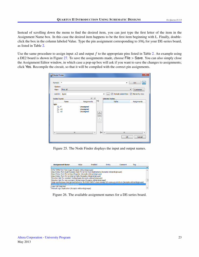
Pin assignments are made by using the Assignment Editor. Select Assignments > Assignment Editor to reach thewindow in Figure 24 (shown here as a detached window). In the Category drop-down menu select All. Click onthe <<new>> button located near the top left corner to make a new item appear in the table. Double click the boxunder the column labeled To so that the Node Finder button appears. Click on the button (not the drop downarrow) to reach the window in Figure 25. Click on to show more search options. In the Filter drop-down menuselect Pins: all. Then click the List button to display the input and output pins to be assigned: f , x1, and x2. Clickon x1 as the first pin to be assigned and click the > button; this will enter x1 in the Selected Nodes box. Click OK.x1 will now appear in the box under the column labeled To. Alternatively, the node name can be entered directly bydouble-clicking the box under the To column and typing in the node name.
Follow this by double-clicking on the box to the right of this new x1 entry, in the column labeled Assignment Name.Now, the drop-down menu in Figure 26 appears. Scroll down and select Location (Accepts wildcards/groups).
22 Altera Corporation - University ProgramMay 2013
QUARTUS II INTRODUCTION USING SCHEMATIC DESIGNS For Quartus II 13.0
Instead of scrolling down the menu to find the desired item, you can just type the first letter of the item in theAssignment Name box. In this case the desired item happens to be the first item beginning with L. Finally, double-click the box in the column labeled Value. Type the pin assignment corresponding to SW0 for your DE-series board,as listed in Table 2.
Use the same procedure to assign input x2 and output f to the appropriate pins listed in Table 2. An example usinga DE2 board is shown in Figure 27. To save the assignments made, choose File > Save. You can also simply closethe Assignment Editor window, in which case a pop-up box will ask if you want to save the changes to assignments;click Yes. Recompile the circuit, so that it will be compiled with the correct pin assignments.
Figure 25. The Node Finder displays the input and output names.
Figure 26. The available assignment names for a DE-series board.
QUARTUS II INTRODUCTION USING SCHEMATIC DESIGNS For Quartus II 13.0
Figure 27. The complete assignment.
The DE-series board has fixed pin assignments. Having finished one design, the user will want to use the same pinassignment for subsequent designs. Going through the procedure described above becomes tedious if there are manypins used in the design. A useful Quartus II feature allows the user to both export and import the pin assignmentsfrom a special file format, rather than creating them manually using the Assignment Editor. A simple file formatthat can be used for this purpose is the Quartus II Settings File (QSF) format. The format for the file for our simpleproject (on a DE2 board) is
set_location_assignment PIN_N25 -to x1set_location_assignment PIN_N26 -to x2set_location_assignment PIN_AE22 -to f
By adding lines to the file, any number of pin assignments can be created. Such qsf files can be imported into anydesign project.
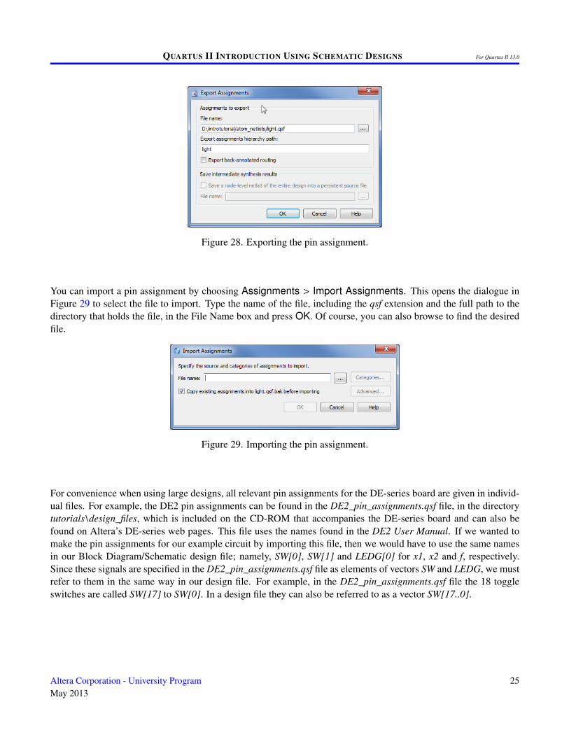
If you created a pin assignment for a particular project, you can export it for use in a different project. To see howthis is done, open again the Assignment Editor to reach the window in Figure 27. Select Assignments > ExportAssignment which leads to the window in Figure 28. Here, the file light.qsf is available for export. Click on OK. Ifyou now look in the directory, you will see that the file light.qsf has been created.
24 Altera Corporation - University ProgramMay 2013
QUARTUS II INTRODUCTION USING SCHEMATIC DESIGNS For Quartus II 13.0
Figure 28. Exporting the pin assignment.
You can import a pin assignment by choosing Assignments > Import Assignments. This opens the dialogue inFigure 29 to select the file to import. Type the name of the file, including the qsf extension and the full path to thedirectory that holds the file, in the File Name box and press OK. Of course, you can also browse to find the desiredfile.
Figure 29. Importing the pin assignment.
For convenience when using large designs, all relevant pin assignments for the DE-series board are given in individ-ual files. For example, the DE2 pin assignments can be found in the DE2_pin_assignments.qsf file, in the directorytutorials\design_files, which is included on the CD-ROM that accompanies the DE-series board and can also befound on Altera’s DE-series web pages. This file uses the names found in the DE2 User Manual. If we wanted tomake the pin assignments for our example circuit by importing this file, then we would have to use the same namesin our Block Diagram/Schematic design file; namely, SW[0], SW[1] and LEDG[0] for x1, x2 and f, respectively.Since these signals are specified in the DE2_pin_assignments.qsf file as elements of vectors SW and LEDG, we mustrefer to them in the same way in our design file. For example, in the DE2_pin_assignments.qsf file the 18 toggleswitches are called SW[17] to SW[0]. In a design file they can also be referred to as a vector SW[17..0].
QUARTUS II INTRODUCTION USING SCHEMATIC DESIGNS For Quartus II 13.0
8 Simulating the Designed Circuit
Before implementing the designed circuit in the FPGA chip on the DE-series board, it is prudent to simulate it toascertain its correctness. Quartus II’s Simulation Waveform Editor tool can be used to simulate the behavior ofa designed circuit. Before the circuit can be simulated, it is necessary to create the desired waveforms, called testvectors, to represent the input signals. It is also necessary to specify which outputs, as well as possible internal pointsin the circuit, the designer wishes to observe. The simulator applies the test vectors to a model of the implementedcircuit and determines the expected response. We will use the Simulation Waveform Editor to draw the test vectors,as follows:
1. In the main Quartus II window, select File > New > Verification/Debugging Files > University ProgramVWF to open the Simulation Waveform Editor.
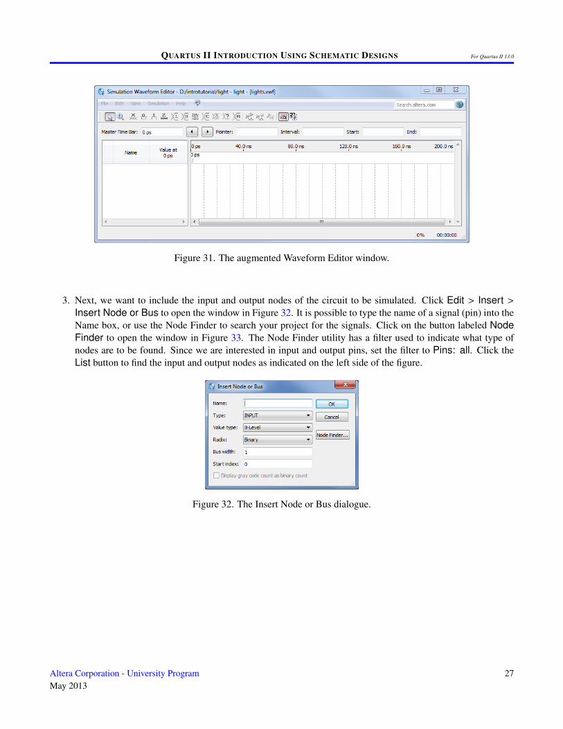
2. The Simulation Waveform Editor window is depicted in Figure 30. Save the file under the name light.vwf;note that this changes the name in the displayed window. Set the desired simulation to run from 0 to 200 ns byselecting Edit > Set End Time and entering 200 ns in the dialog box that pops up. Selecting View > Fit inWindow displays the entire simulation range of 0 to 200 ns in the window, as shown in Figure 31. You maywish to resize the window to its maximum size.
Figure 30. The Waveform Editor window.
26 Altera Corporation - University ProgramMay 2013
QUARTUS II INTRODUCTION USING SCHEMATIC DESIGNS For Quartus II 13.0
Figure 31. The augmented Waveform Editor window.
3. Next, we want to include the input and output nodes of the circuit to be simulated. Click Edit > Insert >Insert Node or Bus to open the window in Figure 32. It is possible to type the name of a signal (pin) into theName box, or use the Node Finder to search your project for the signals. Click on the button labeled NodeFinder to open the window in Figure 33. The Node Finder utility has a filter used to indicate what type ofnodes are to be found. Since we are interested in input and output pins, set the filter to Pins: all. Click theList button to find the input and output nodes as indicated on the left side of the figure.
QUARTUS II INTRODUCTION USING SCHEMATIC DESIGNS For Quartus II 13.0
Figure 33. Selecting nodes to insert into the Waveform Editor.
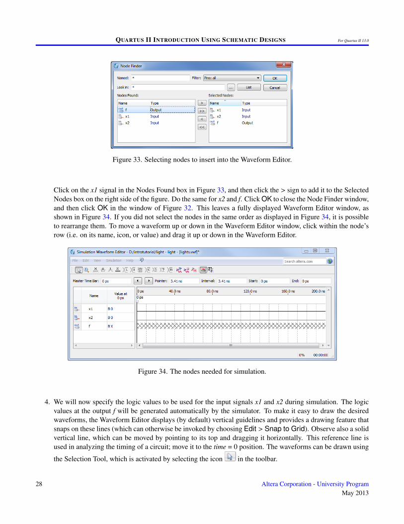
Click on the x1 signal in the Nodes Found box in Figure 33, and then click the > sign to add it to the SelectedNodes box on the right side of the figure. Do the same for x2 and f. Click OK to close the Node Finder window,and then click OK in the window of Figure 32. This leaves a fully displayed Waveform Editor window, asshown in Figure 34. If you did not select the nodes in the same order as displayed in Figure 34, it is possibleto rearrange them. To move a waveform up or down in the Waveform Editor window, click within the node’srow (i.e. on its name, icon, or value) and drag it up or down in the Waveform Editor.
Figure 34. The nodes needed for simulation.
4. We will now specify the logic values to be used for the input signals x1 and x2 during simulation. The logicvalues at the output f will be generated automatically by the simulator. To make it easy to draw the desiredwaveforms, the Waveform Editor displays (by default) vertical guidelines and provides a drawing feature thatsnaps on these lines (which can otherwise be invoked by choosing Edit > Snap to Grid). Observe also a solidvertical line, which can be moved by pointing to its top and dragging it horizontally. This reference line isused in analyzing the timing of a circuit; move it to the time = 0 position. The waveforms can be drawn using
the Selection Tool, which is activated by selecting the icon in the toolbar.
28 Altera Corporation - University ProgramMay 2013
QUARTUS II INTRODUCTION USING SCHEMATIC DESIGNS For Quartus II 13.0
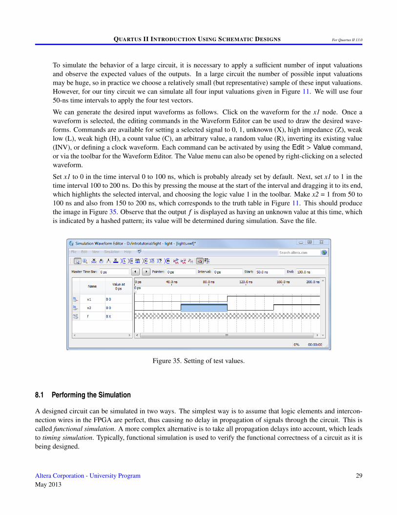
To simulate the behavior of a large circuit, it is necessary to apply a sufficient number of input valuationsand observe the expected values of the outputs. In a large circuit the number of possible input valuationsmay be huge, so in practice we choose a relatively small (but representative) sample of these input valuations.However, for our tiny circuit we can simulate all four input valuations given in Figure 11. We will use four50-ns time intervals to apply the four test vectors.
We can generate the desired input waveforms as follows. Click on the waveform for the x1 node. Once awaveform is selected, the editing commands in the Waveform Editor can be used to draw the desired wave-forms. Commands are available for setting a selected signal to 0, 1, unknown (X), high impedance (Z), weaklow (L), weak high (H), a count value (C), an arbitrary value, a random value (R), inverting its existing value(INV), or defining a clock waveform. Each command can be activated by using the Edit > Value command,or via the toolbar for the Waveform Editor. The Value menu can also be opened by right-clicking on a selectedwaveform.
Set x1 to 0 in the time interval 0 to 100 ns, which is probably already set by default. Next, set x1 to 1 in thetime interval 100 to 200 ns. Do this by pressing the mouse at the start of the interval and dragging it to its end,which highlights the selected interval, and choosing the logic value 1 in the toolbar. Make x2 = 1 from 50 to100 ns and also from 150 to 200 ns, which corresponds to the truth table in Figure 11. This should producethe image in Figure 35. Observe that the output f is displayed as having an unknown value at this time, whichis indicated by a hashed pattern; its value will be determined during simulation. Save the file.
Figure 35. Setting of test values.
8.1 Performing the Simulation
A designed circuit can be simulated in two ways. The simplest way is to assume that logic elements and intercon-nection wires in the FPGA are perfect, thus causing no delay in propagation of signals through the circuit. This iscalled functional simulation. A more complex alternative is to take all propagation delays into account, which leadsto timing simulation. Typically, functional simulation is used to verify the functional correctness of a circuit as it isbeing designed.
QUARTUS II INTRODUCTION USING SCHEMATIC DESIGNS For Quartus II 13.0
8.1.1 Functional Simulation
Before running a functional simulation it is necessary to run Analysis and Synthesis on your design by selecting the
icon in the main Quartus II window. Note that Analysis and Synthesis gets run as a part of the main compilationflow. If you compiled your design in Section 6, then it is not necessary to run Analysis and Synthesis again.
To perform the functional simulation, select Simulation > Run Functional Simulation or select the icon. Apop-up window will show the progress of the simulation then automatically close when it is complete. At the end ofthe simulation, a second Waveform Editor window will open the results of the simulation as illustrated in Figure 36.Observe that the output f is as specified in the truth table of Figure 11.
Figure 36. The result of functional simulation.
8.1.2 Timing Simulation
Having ascertained that the designed circuit is functionally correct, we should now perform the timing simulationto see how it will behave when it is actually implemented in the chosen FPGA device. Before running a timing
simulation, it is necessary to compile your design by selecting the icon in the main Quartus II window. Un-like functional simulations, timing simulations require the full compilation of your design, not just Analysis andSynthesis.
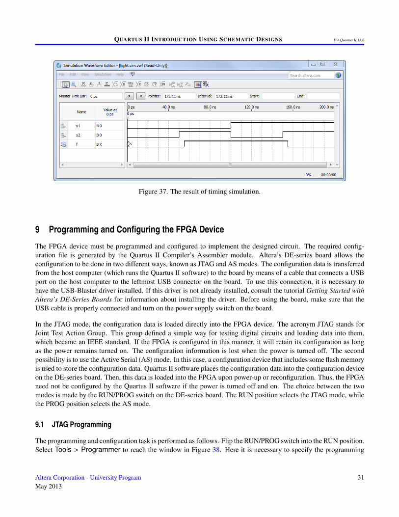
To perform the timing simulation, select Simulation > Run Timing Simulation or select the icon. Thesimulation should produce the waveforms in Figure 37. Observe that there is a delay of about 5 ns in producing achange in the signal f from the time when the input signals, x1 and x2, change their values. This delay is due to thepropagation delays in the logic element and the wires in the FPGA device.
30 Altera Corporation - University ProgramMay 2013
QUARTUS II INTRODUCTION USING SCHEMATIC DESIGNS For Quartus II 13.0
Figure 37. The result of timing simulation.
9 Programming and Configuring the FPGA Device
The FPGA device must be programmed and configured to implement the designed circuit. The required config-uration file is generated by the Quartus II Compiler’s Assembler module. Altera’s DE-series board allows theconfiguration to be done in two different ways, known as JTAG and AS modes. The configuration data is transferredfrom the host computer (which runs the Quartus II software) to the board by means of a cable that connects a USBport on the host computer to the leftmost USB connector on the board. To use this connection, it is necessary tohave the USB-Blaster driver installed. If this driver is not already installed, consult the tutorial Getting Started withAltera’s DE-Series Boards for information about installing the driver. Before using the board, make sure that theUSB cable is properly connected and turn on the power supply switch on the board.
In the JTAG mode, the configuration data is loaded directly into the FPGA device. The acronym JTAG stands forJoint Test Action Group. This group defined a simple way for testing digital circuits and loading data into them,which became an IEEE standard. If the FPGA is configured in this manner, it will retain its configuration as longas the power remains turned on. The configuration information is lost when the power is turned off. The secondpossibility is to use the Active Serial (AS) mode. In this case, a configuration device that includes some flash memoryis used to store the configuration data. Quartus II software places the configuration data into the configuration deviceon the DE-series board. Then, this data is loaded into the FPGA upon power-up or reconfiguration. Thus, the FPGAneed not be configured by the Quartus II software if the power is turned off and on. The choice between the twomodes is made by the RUN/PROG switch on the DE-series board. The RUN position selects the JTAG mode, whilethe PROG position selects the AS mode.
9.1 JTAG Programming
The programming and configuration task is performed as follows. Flip the RUN/PROG switch into the RUN position.Select Tools > Programmer to reach the window in Figure 38. Here it is necessary to specify the programming
QUARTUS II INTRODUCTION USING SCHEMATIC DESIGNS For Quartus II 13.0
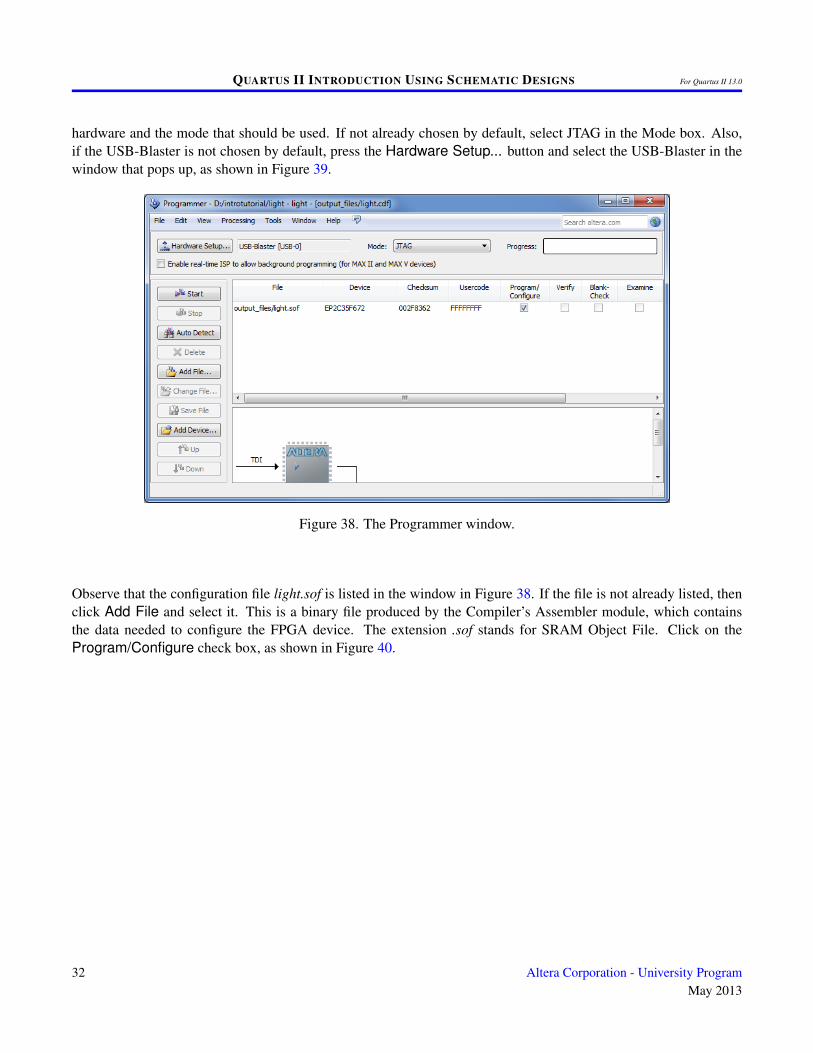
hardware and the mode that should be used. If not already chosen by default, select JTAG in the Mode box. Also,if the USB-Blaster is not chosen by default, press the Hardware Setup... button and select the USB-Blaster in thewindow that pops up, as shown in Figure 39.
Figure 38. The Programmer window.
Observe that the configuration file light.sof is listed in the window in Figure 38. If the file is not already listed, thenclick Add File and select it. This is a binary file produced by the Compiler’s Assembler module, which containsthe data needed to configure the FPGA device. The extension .sof stands for SRAM Object File. Click on theProgram/Configure check box, as shown in Figure 40.
32 Altera Corporation - University ProgramMay 2013
QUARTUS II INTRODUCTION USING SCHEMATIC DESIGNS For Quartus II 13.0
Figure 39. The Hardware Setup window.
Figure 40. The updated Programmer window.
Now, press Start in the window in Figure 40. An LED on the board will light up when the configuration data hasbeen downloaded successfully. If you see an error reported by Quartus II software indicating that programmingfailed, then check to ensure that the board is properly powered on.
QUARTUS II INTRODUCTION USING SCHEMATIC DESIGNS For Quartus II 13.0
9.2 Active Serial Mode Programming
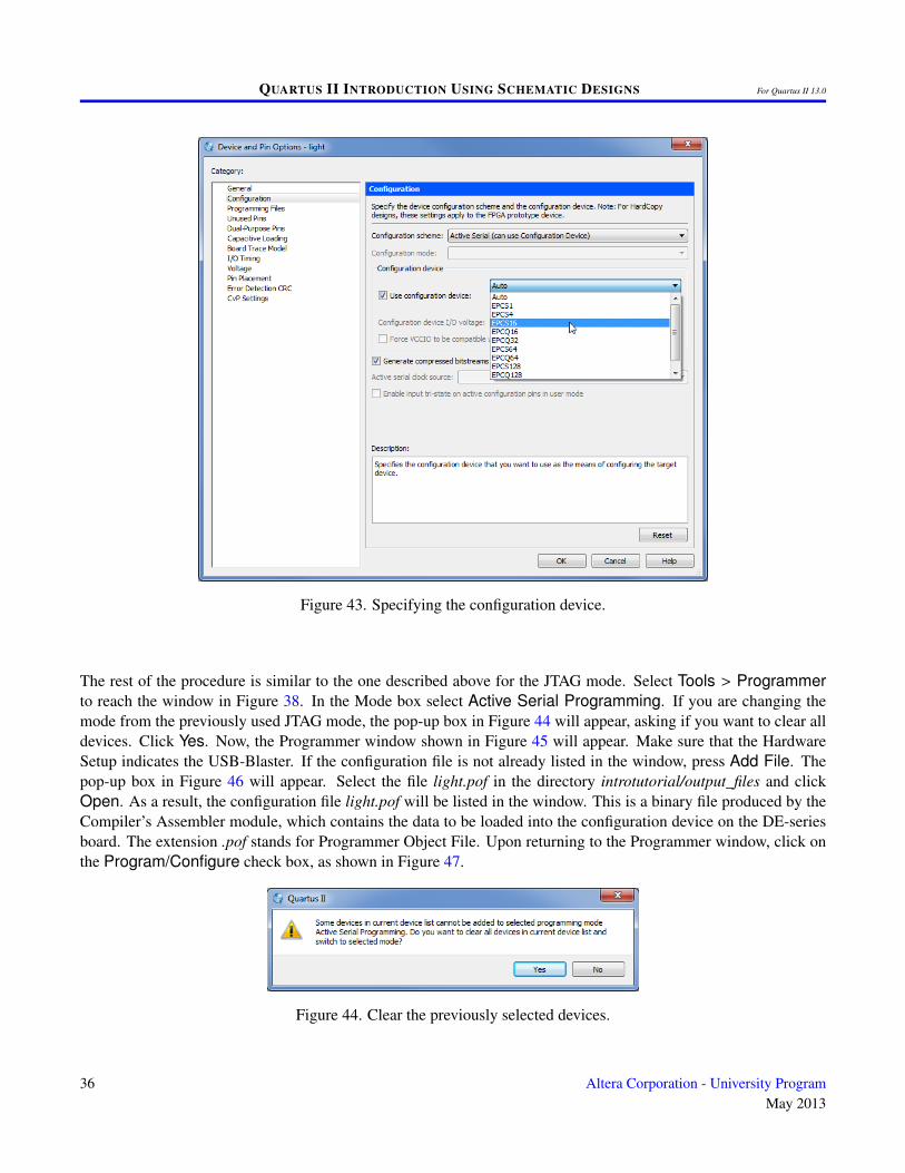
In this case, the configuration data has to be loaded into the configuration device on the DE-series board. Refer toTable 3 for a list of configuration devices on DE-series boards. To specify the required configuration device selectAssignments > Device, which leads to the window in Figure 41. Click on the Device and Pin Options buttonto reach the window in Figure 42. Now, click on Configuration in the menu on the left to obtain the window inFigure 43. In the Configuration device box (which may be set to Auto) choose the correct configuration device nameand click OK. Upon returning to the window in Figure 41, click OK. Recompile the designed circuit.
Board Configuration DeviceDE0 EPCS4
DE0-Nano EPCS64DE1 EPCS4DE2 EPCS16
DE2-70 EPCS64DE2-115 EPCS64
Table 3. DE-series Configuration Device Names
Figure 41. The Device Settings window.
34 Altera Corporation - University ProgramMay 2013
QUARTUS II INTRODUCTION USING SCHEMATIC DESIGNS For Quartus II 13.0
Figure 43. Specifying the configuration device.
The rest of the procedure is similar to the one described above for the JTAG mode. Select Tools > Programmerto reach the window in Figure 38. In the Mode box select Active Serial Programming. If you are changing themode from the previously used JTAG mode, the pop-up box in Figure 44 will appear, asking if you want to clear alldevices. Click Yes. Now, the Programmer window shown in Figure 45 will appear. Make sure that the HardwareSetup indicates the USB-Blaster. If the configuration file is not already listed in the window, press Add File. Thepop-up box in Figure 46 will appear. Select the file light.pof in the directory introtutorial/output_files and clickOpen. As a result, the configuration file light.pof will be listed in the window. This is a binary file produced by theCompiler’s Assembler module, which contains the data to be loaded into the configuration device on the DE-seriesboard. The extension .pof stands for Programmer Object File. Upon returning to the Programmer window, click onthe Program/Configure check box, as shown in Figure 47.
Figure 44. Clear the previously selected devices.
36 Altera Corporation - University ProgramMay 2013
QUARTUS II INTRODUCTION USING SCHEMATIC DESIGNS For Quartus II 13.0
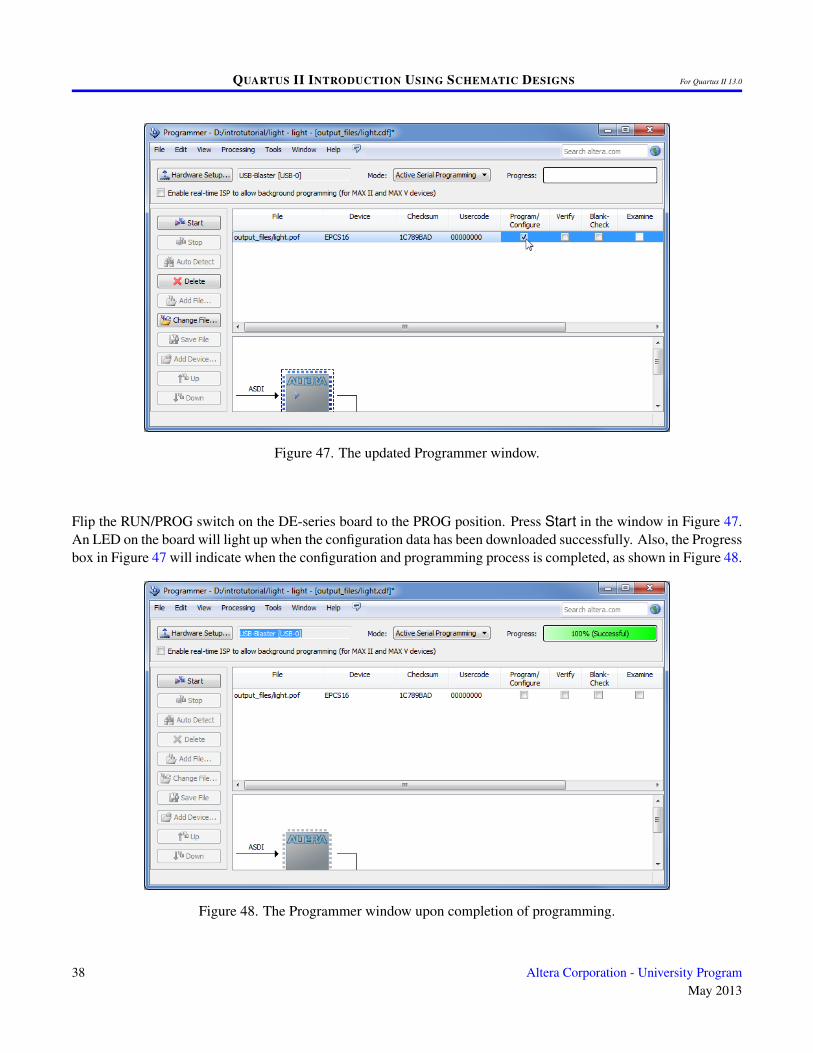
Figure 47. The updated Programmer window.
Flip the RUN/PROG switch on the DE-series board to the PROG position. Press Start in the window in Figure 47.An LED on the board will light up when the configuration data has been downloaded successfully. Also, the Progressbox in Figure 47 will indicate when the configuration and programming process is completed, as shown in Figure 48.
Figure 48. The Programmer window upon completion of programming.
38 Altera Corporation - University ProgramMay 2013
QUARTUS II INTRODUCTION USING SCHEMATIC DESIGNS For Quartus II 13.0
10 Testing the Designed Circuit
Having downloaded the configuration data into the FPGA device, you can now test the implemented circuit. Flipthe RUN/PROG switch to RUN position. Try all four valuations of the input variables x1 and x2, by setting thecorresponding states of the switches SW1 and SW0. Verify that the circuit implements the truth table in Figure 11.
If you want to make changes in the designed circuit, first close the Programmer window. Then make the desiredchanges in the Block Diagram/Schematic file, compile the circuit, and program the board as explained above.
This document is being provided on an “as-is” basis and as an accommodation and therefore all warranties, repre-sentations or guarantees of any kind (whether express, implied or statutory) including, without limitation, warrantiesof merchantability, non-infringement, or fitness for a particular purpose, are specifically disclaimed.
40 Altera Corporation - University ProgramMay 2013