I2C BUS Serial Interface RTC with High-precision Oscillation Adjustment BU9873
Outline
The BU9873 is a CMOS real-time clock, which has a built-in interrupt generation function. This product is connected to the CPU via I2C interface, and configured to perform serial transmission of time and calendar data to the CPU. A high-precision oscillation adjustment circuit is also integrated, which is capable of adjusting time counts with digital method, and correcting deviations in the oscillation frequency of the crystal oscillator.
Features
■ Connected to the CPU via I2C Interface
■ Time (Hour・Minute・Second, Selectable 12-Hour
and 24-Hour Mode Setting)
■ Calendar (Year・Month・Day・Week)
■ Periodic Interrupt Function (Output from INTRB, Ranging from 1 Second to 1 Month)
■ Alarm Interrupt Function
(Day-of-Week ・ Hour ・ Minute in Setting Format,
Output from INTRB)
■ Oscillation Halt Sensing Function
■ 32.768 kHz Clock Output (Output from 32KOUT with Control Register)
■ ±30 Second Adjustment Function
■ Automatic Leap Year Recognition up to the Year 2099
The above circuits do not guarantee operation. Set the circuits and constants after performing sufficient evaluation using the actual application. And please arrange the circuits to keep “Notes during Power On”. If it is necessary, please use the discharge circuits of battery to keep it.
1 32KOUT Output The 32KOUT pin is used to output 32.768 kHz clock pulses, which is controlled by an internal register. This pin is enabled during power-on from 0V, and is CMOS push-pull output.
2 SCL Input The SCL pin is used to input clock pulses synchronizing the input/output data from SDA pin.
3 SDA Input/Output The SDA pin is used to input and output data for writing and reading, which is synchronized with SCL pin. This pin is N-channel open drain output.
4 VSS - The VSS pin is grounded.
5 INTRB Output The INTRB pin is used to output periodic interrupt, or alarm interrupt (Alarm_A, Alarm_B) to the CPU. This pin is disabled during power-on from 0V, and is also N-channel open drain output.
6 OSCOUT - The OSCIN and OSCOUT pins are used to connect the 32.768 kHz crystal oscillator (Beside the crystal, all other oscillation circuit components is already integrated in this IC). 7 OSCIN -
8 VDD - The VDD pin is connected to the power supply.
0.45 (SOP-J8) When using above Ta=25, decreased by 4.5mW/°C.
0.33 (TSSOP-B8) When using above Ta=25, decreased by 3.3mW/°C.
0.31 (MSOP8) When using above Ta=25, decreased by 3.1mW/°C.
0.30 (VSON008X2030) When using above Ta=25, decreased by 3.0mW/°C.
Storage Temperature
Tstg -55 to +125 °C
Operating Temperature
Topt -40 to +85 °C
Terminal Voltage ― -0.3 to VDD +0.3 V The Max value of Terminal Voltage is not over 6.5V.
When the pulse width is 50ns or less, the Min value of
Terminal Voltage is not lower than -0.8V.
Caution: Operating the IC over the absolute maximum ratings may damage the IC. In addition, it is impossible to predict all destructive situations such as
short-circuit modes, open circuit modes, etc. Therefore, it is important to consider circuit protection measures, like adding a fuse, in case the IC is operated in a
special mode exceeding the absolute maximum ratings
Operating Conditions
Item Symbol Rating Unit
Supply Voltage VDD 1.8 to 5.5 V
Timekeeping Voltage(Note 1)
VCLK 1.45 to 5.5 V
Input Voltage VIN 0 to VDD V
(Note1) For minimum time keeping voltage, CGOUT = CDOUT = 0 pF; Quartz crystal unit: CL (load capacitor) = 6 pF to 12.5 pF, Maximum value of R1 (equivalent
IC function will be explained as the following sequence. 1. Communication interface 2. Address mapping of internal register 3. Clock and calendar function 4. Oscillation adjustment function with digital method 5. Alarm interrupts function 6. Periodic interrupt function 7. Test bit 8. ±30 second adjust function 9. Oscillation halts sensing function 10. 32-kHz clock output function
This product can read/write data from I2C bus interface with 2-wires: SDA (data) and SCL (clock). Since the output of SDA
pin is open-drain, data transferring between CPU with different supply voltage is possible by adopting a pull-up resistor on the circuit board.
1-1. I2C BUS Communication
I2C BUS data communication starts by a start condition input, and ends by a stop condition input. The data length is 8-bit,
and acknowledges signal is always required after each byte. I2C BUS carries out data transmission between plural devices connected by 2-wires: serial data (SDA) and serial clock
(SCL). Among these devices, there is “master” that generates clock and control the start and end signal, and “slave” that is controlled by unique device address. RTC is “slave”. And the device that outputs data to bus during data transferring is called “transmitter”, and the device that receives data is called “receiver”.
Figure 17. I2C BUS communication 1-2. Start Condition (start bit recognition)
Before executing any command, start condition (start bit) is necessary, where SDA goes from “H” down to “L” when SCL is “H”. This IC always detects whether SDA and SCL are in start condition (start bit) or not, therefore, unless this condition is satisfied, no command will be executed.
1-3. Stop Condition (stop bit recognition)
Every command can be ended by stop condition (stop bit), where SDA rising from “L” to “H” when SCL is “H”.
1-4. Acknowledge (ACK) Signal
・This acknowledge (ACK) signal is a software rule to judge whether data transfer has been executed successfully or not. For
master and slave, the device (µ-COM during inputting slave address of write command, read command, and this IC during outputting data of read command) at the transmitter side releases the bus after outputting 8-bit data.
・The device (this IC during inputting slave address of write command, read command, and µ-COM during outputting data of
read command) at the receiver side sets SDA “L” during the ninth clock cycle, and outputs acknowledge signal (ACK) showing that it has received the 8-bit data.
・This IC outputs acknowledge signal (ACK) “L” after recognizing start condition and 8-bit slave address.
・Every write action outputs acknowledge signal (ACK) “L” after receiving 8-bit data (word address and write data).
・Every read action outputs 8-bit data (read data), and detects acknowledge signal (ACK) “L”. When acknowledge signal
(ACK) is detected, and stop condition is not sent from the master (µ-COM) side, this IC will continue to output data. When acknowledge signal (ACK) is not detected, this IC will stop data transfer, and end read action after recognizing stop condition (stop bit). Then, this IC will get in off-status.
Write command is illustrated as following: Firstly, input start condition; then, enter the 7-bit slave address. Slave address of
this IC is (0110010). Thereafter, enter “L” for the R/W――
bit, which indicates the direction of data transmission. In the next byte, input the internal address pointer (4-bit) and transmission format (4-bit) to the IC. For write operation, only
one transmission format (0000) is available. The 3rd byte transmits data that will be written to the address specified by the internal address pointer. Internal address pointer settings will also be automatically incremented for 4byte and after. Note that when the internal address pointer is Fh, it will change to 0h during transmitting the next byte. Example of write command (when writing to internal address Eh to Fh)
Figure 18. Write command 1-6. Read Command
This IC allows the following three methods of reading data from an internal register.
1-6-1. Read from a Specified Internal Address
The first method uses data write command to specify the internal address pointer and transfer format, and then repeat the
start condition again. After the 7-bit slave address, enter “H” for the R/ W bit, which indicates the direction of data
transmission. In the next byte, data from the specified internal address will be output. If entering “L” during the timing of ACK, the data from the next address will be output continuously. The read operation will not be ended until entering “H” during the timing of ACK and following a stop condition.
The internal address pointer is reset to Fh when a stop condition is met. Therefore, this read method allows no insertion of stop condition before the end of read.
Example 1 of data read (when data is read from 2h to 3h)
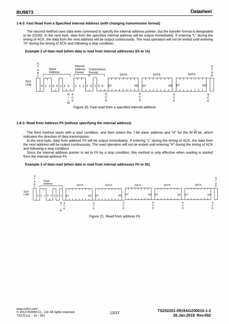
1-6-2. Fast Read from a Specified Internal Address (with changing transmission format)
The second method uses data write command to specify the internal address pointer, but the transfer format is designated
to be (0100). In the next byte, data from the specified internal address will be output immediately. If entering “L” during the timing of ACK, the data from the next address will be output continuously. The read operation will not be ended until entering “H” during the timing of ACK and following a stop condition.
Example 2 of data read (when data is read from internal addresses Eh to 1h)
Figure 20. Fast read from a specified internal address 1-6-3. Read from Address Fh (without specifying the internal address)
The third method starts with a start condition, and then enters the 7-bit slave address and “H” for the R/ W bit, which
indicates the direction of data transmission. In the next byte, data from address Fh will be output immediately. If entering “L” during the timing of ACK, the data from
the next address will be output continuously. The read operation will not be ended until entering “H” during the timing of ACK and following a stop condition
Since the internal address pointer is set to Fh by a stop condition, this method is only effective when reading is started from the internal address Fh.
Example 3 of data read (when data is read from internal addresses Fh to 3h)
To avoid invalid read and write, two features should be noted when accessing the RTC.
Hold function of clock carry-up
While read and write operation is executed (at the same time, RTC clock is still counting-up), this IC temporarily holds the
clock carry-up from start condition to stop condition, to prevent invalid read and write. If clock carry-up happens during this period (read or write from start condition to stop condition), it will be adjusted within approx. 61μs after stop condition.
Automatic release function of access
When 0.5 to 1.0 second elapses after start condition, any access to the RTC will be automatically terminated, to release
the temporarily holding of clock carry-up, set Fh to the address pointer, and access from the CPU is forced to be stopped (as long as stop condition is received, the same action will be made: automatic release function from the I2C bus interface).
Therefore, one access must be completed within 0.5 seconds. The automatic release function prevents delay in SCL clock, even if SCL is stopped because of system sudden failure during read operation.
In addition, a second start condition (after the first start condition and ahead of the stop condition) is regarded as the “repeated start condition”. Therefore, when 0.5 to 1.0 seconds elapses after the first start condition, access to the RTC will also be released automatically.
If access is tried after automatic release function is activated, no acknowledge signal will be output for writing while FFh will be output for reading.
The following points should be noted during accessing the RTC. (1) No stop condition shall be generated until clock and calendar data read/write is started and completed
Bad example of time read (Start condition) → (Read of seconds) → (Read of minutes) → (Stop condition) → (Start condition) → (Read of hours) → (Stop condition)
Assuming read is started at 05:59:59 P.M. and while reading seconds and minutes the time advanced to 06:00:00 P.M. During this time, second digit is hold so the read result is 05:59:59. Then the IC confirms stop condition and carries second digit that is being hold and the time changes to 06:00:00 P.M. Thus, when the hour digit is read, it changes to be 6. The invalid results of 06:59:59 will be read.
(2) One cycle of read/write operation shall be completed within 0.5 seconds. (3) Do not send start condition within 61μs from stop condition, because the clock carry-up that is hold during I2C access
will be adjusted within approx.61μs from stop condition.
E 1 1 1 0 Control Register 1 AALE BALE — — TEST (Note4)
CT2 CT1 CT0
F 1 1 1 1 Control Register 2 — — 12B/24
ADJ (Note2)
XSTP (Note3)
CLENB CTFG AAFG BAFG
(Note1) The “–” mark indicates data which can be read only and set to “0” when it is read.
(Note2) For the ADJ/XSTP bit of control register 2, ADJ will be set to “1” if writing “1”, while XSTP will be set to “0” if writing “0” during normal oscillation.
Conversely, setting ADJ=0 and XSTP=1 cause no event. The value of XSTP bit is output when it is read.
(Note3) When XSTP is set to “1”, the internal register F6 to F0, CT2 to CT0, AALE, BALE, CLENB will be reset to “0”.
(Note4) The TEST bit of control register 1 is for shipment testing. Please always set TEST = 0. If this bit is set to “1” accidentally, it will be reset to “0” after stop
The clock and calendar function is available in this IC, ranging from seconds to years (the last two digits of a year). Every register is configured in BCD code, and assigned to the following address respectively. Second counter (internal address 0h) Minute counter (internal address 1h) Hour counter (internal address 2h) Day-of-week counter (internal address 3h) Day counter (internal address 4h) Month counter (internal address 5h) Year counter (internal address 6h)
3-1. Clock Counter (second counter, minute counter and hour counter)
Time digit in BCD code is displayed as follows. Second counter: be reset to “00” and carried to minute digits when incremented from 00 to 59. Minute counter: be reset to “00” and carried to hour digits when incremented from 00 to 59. Hour counter: be reset to “00” and carried to day and day-of-the-week digits when incremented from 00 to 23 (in 24-hour mode). If non-existent time has been written, any carry from lower digits may cause the time counters to malfunction. Therefore, such incorrect writing should be replaced with the writing of existent time data. Users can choose to display time in 12-hour mode or 24-hour mode by setting the 12B/24 bit (internal address Fh).
12B/24-hour mode selection bit
12B/24 Description
0 12- hour time display system (separate for morning and afternoon)
Setting the 12-hour or 24-hour mode should precede writing time data.
3-2. Day-of-week Counter
Day-of-week digits are incremented by 1 corresponding to the 7 days of week, e.g. (W4, W2, W1) = (0, 0, 0) → (0, 0, 1) → … → (1, 1, 0) → (0, 0, 0) The relation between the days of week and day-of-week digits is user definable. (e.g. Sunday=0, 0, 0) (W4, W2, W1) should not be set to (1, 1, 1).
3-3. Calendar Counter (day counter, month counter and year counter)
The automatic calendar function provides the calendar digit displayed in BCD code.
Day digits: Range from 1 to 31 (for January, March, May, July, August, October, and December) Range from 1 to 30 (for April, June, September, and November) Range from 1 to 29 (for February in leap years) Range from 1 to 28 (for February in ordinary years) Carried to month digits when reset to 1
Month digits: Range from 1 to 12 and carried to year digits when reset to 1. Year digits: Range from 00 to 99 and 00, 04, 08… 92 and 96 are counted as leap years.
If non-existent time has been written, any carry from lower digits may cause the time counters to malfunction. Therefore, such incorrect writing should be replaced with the writing of existent time data.
Automatic judgment function of leap year is included in this IC. Leap year is defined as follows. The year that can be divided by 4 is leap year. The year that can be divided by 100 is ordinary year. The year that can be divided by 400 is leap year. For example, year 2000 is a leap year while year 2100 is ordinary year. Because the year register of this IC only supports the last two digits, a year will be automatically recognized as a leap year if it is a multiple of 4. Therefore, year 2100 or 2000 will be determined as leap year because the last two digits are “00”. This result in automatic judgment of leap years only can be up to the year 2099 in this IC.
4. Oscillation Adjustment Function with Digital Method
This IC has built-in oscillation capacitance CG and CD, the oscillation circuit can be configured easily by connecting an
external crystal oscillator. However, due to some variations such as parasitic capacitance, it is hardly for RTC to oscillate at 32,768 Hz exactly.
Therefore, if you want to achieve high-precision clock, it is necessary to use the error correction method. By using this feature, you can achieve high-precision clock with only ±1.5ppm mismatch at a specified temperature. Because the crystal oscillator has temperature dependency, the clock mismatch will increase when the temperature changes.
The clock adjustment step is about 3ppm and the total range is ±189ppm. As following, some application is possible: (1) If the temperature sensor is integrated in system, by setting the clock adjustment function in accordance with the
variation of temperature, it is possible to realize high-precision clock that does not depend on the temperature. (2) By storing seasonal temperature information to the system, and using the clock adjustment function with this
temperature information, the realization of high-precision clock is available throughout the year. 4-1. Function Description
In the IC, counting up to seconds is made once per 32,768 of clock pulse generated by the oscillator. If oscillation
frequency is not 32,768 Hz which does not match with the number of clock counts, the time error will happen. This function is designated to compensate the clock mismatch.
The adjustment function adds 2 clock pulses every 20 seconds: 2/(32,768×20)=3.051ppm, which delays the clock by approx. 3ppm. Likewise, decrementing 2 clock pulses advances the clock by 3ppm. Thus the clock may be adjusted to the precision of ±1.5ppm. and the total range is ±189.2ppm (±124 steps) according to the internal 7-bit trim register. The time trimming circuit adjusts one second count based on this register when second digit is 00, 20 or 40 seconds. Note that the time trimming function only adjust clock timing and oscillation frequency and 32-kHz clock output is not adjusted.
Setting data to internal register (internal address 7h) activates the time trimming circuit. And bit F6 decides either
increasing or decreasing the clock pulse.
The clock counts will be increased as ((F5, F4, F3, F2, F1, F0)-1) ×2 when F6 is set to “0”.
The clock counts will be decreased as ((/F5, /F4, /F3, /F2, /F1, /F0)+1) ×2 when F6 is set to “1”.
Counts will not change when (F6, F5, F4, F3, F2, F1, F0) are set to (*, 0, 0, 0, 0, 0, *) For example, when 32.768 kHz crystal is used:
When (F6, F5, F4, F3, F2, F1, F0) are set to (0, 0, 0, 0, 1, 1, 1), counts will change as: 32,768+(7-1) ×2=32,780 (clock will
be delayed) when second digit is 00, 20 or 40. When (F6, F5, F4, F3, F2, F1, F0) are set to (0, 0, 0, 0, 0, 0, 1), counts will remain 32,768 without changing when second digit is 00, 20 or 40.
When (F6, F5, F4, F3, F2, F1, F0) are set to (1, 1, 1, 1, 1, 1, 0), counts will change as: 32,768+(-2) ×2=32,764 (clock will
Time adjustment amount can be calculated following the rules below.
Case 1: When oscillation frequency (Note1) >target frequency (Note2) (clock gains)
(Oscillation frequency − Target frequency + 0.1) Adjustment amount (Note3) = --------------------------------------------------------------
Oscillation frequency × 3.051 × 10⁻⁶
≈ (Oscillation frequency − Target frequency) × 10 + 1
(Note1) Oscillation frequency : Clock frequency output from the 32KOUT pin at room temperature. (Note2) Target frequency : A frequency to be adjusted to. Since temperature characteristics of a 32.768 kHz crystal oscillator generally generates the highest frequency at a room temperature, we recommend to set the target frequency to approx. 32768.00Hz to 32768.10Hz (+3.05ppm to 32768Hz).
Note that this value may differ based on the environment or place where the device will be used. (Note3) Adjustment amount: A value to be set finally to F6 to F0 bits. This value is expressed in 7bit binary digits with sign bit.
Example of Calculations
When oscillation frequency=32768.85 Hz; target frequency=32768.05 Hz
In this instance, write the settings (F6, F5, F4, F3, F2, F1, F0) = (0, 0, 0, 1, 0, 0, 1) in the oscillation adjustment register. Thus, an appropriate oscillation adjustment value in the presence of any time count gain represents a distance from 01h.
Case 2:
When oscillation frequency=target frequency (no clock gain or loss)
(F6, F5, F4, F3, F2, F1, F0) = (*, 0, 0, 0, 0, 0, *). In this case, the correction is not performed.
Case 3:
When oscillation frequency<target frequency (clock loses)
(Oscillation frequency − Target frequency) Adjustment amount = ---------------------------------------------------------
Oscillation frequency × 3.051 × 10⁻⁶
≈(Oscillation frequency - Target frequency) × 10
Example of Calculations
When actual oscillation frequency=32763.95 Hz; target frequency=32768.05 Hz
To express -41 in 7bit binary digits with sign bit, subtract 41 (29h) from 128 (80h) in the above case, 80h-29h=57h. Thus, set (F6, F5, F4, F3, F2, F1, F0) to (1, 0, 1, 0, 1, 1, 1). As this example shows, adjustments to be used when the clock loses shall be distance from 80h.
The BU9873 has an alarm function that outputs an interrupt signal from INTRB pin to CPU when the day of the week, hour or minute match with the preset time. There are two systems of alarms (Alarm_A, Alarm_B), and each may output interrupt signal separately at a specified time. The alarm may be selectable between on and off for each day of the week, thus allowing outputting alarm everyday or on a specific day of the week. Polling is possible for each alarm function
5-1. Usage of Alarm Interrupt Function
Users can set the time to generate an alarm interrupt. There are two systems of alarms, Alarm_A register (internal address 8h to Ah), Alarm_B register (internal address Bh to Dh), covering the day of the week, hour and minute. Because Alarm_A and Alarm_B are the same function, only Alarm_A is explained as example.
Alarm_A, Alarm_B hour register D5 is set to for PM in the 12-hour display system at AP/AB. The register D5 indicates 10 digit of hour digit in 24-hour display system at AH20. To activate alarm operation, any imaginary alarm time setting should not be left to avoid un-matching. AW0 to AW6 correspond to the day-of-the-week counter (W4, W2, W1) being set at (0, 0, 0) to (1, 1, 0). No alarm pulses are output when all of AW0 to AW6 are set to 0.
Example of alarm time settings
Designation of day-of-the-week and AW0 to AW6 in the above table is an example. The alarm interruption is enabled only when the AALE, BALE bits are set to “1” (internal address Eh).
Alarm interrupt output is from INTRB pin and the outputting is “L”. In addition, by monitoring the value of AAFG, BAFG bits (internal address Fh), the state of alarm can be checked.
Alarm_A (Alarm_B) Flag Bit
AAFG, BAFG Description
0 Unmatched alarm register with clock counter Default
1 Matched alarm register with clock counter
The flag bit turns to “1” and INTRB is “L” when matched time is sensed for each alarm. The AAFG, BAFG bit may be set only to “0”. Setting this bit to“0” sets the INTRB to OFF status (“H”). When this bit is set to“1” nothing happens. When the AALE, BALE bit is set to“0”, alarm operation is disabled and “0“is read from the INTRB and AAFG (BAFG) bit.
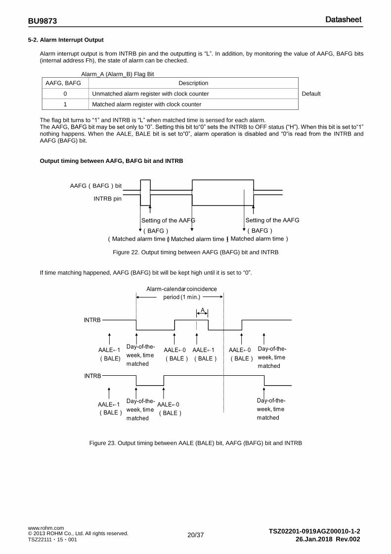
Output timing between AAFG, BAFG bit and INTRB
AAFG(BAFG)bit
INTRB pin
(Matched alarm time)
Setting of the AAFG
(BAFG)
(Matched alarm time)(Matched alarm time)
Setting of the AAFG
(BAFG)
Figure 22. Output timing between AAFG (BAFG) bit and INTRB
If time matching happened, AAFG (BAFG) bit will be kept high until it is set to “0”.
Figure 23. Output timing between AALE (BALE) bit, AAFG (BAFG) bit and INTRB
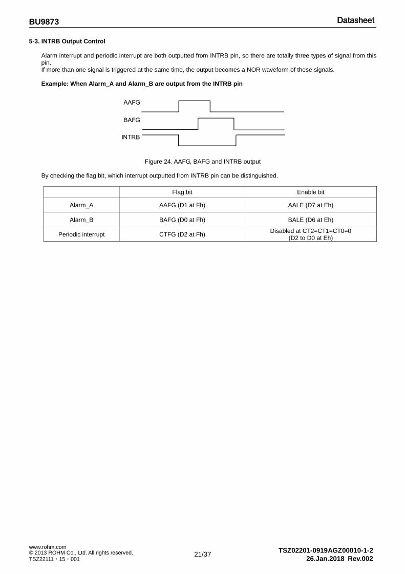
Alarm interrupt and periodic interrupt are both outputted from INTRB pin, so there are totally three types of signal from this pin. If more than one signal is triggered at the same time, the output becomes a NOR waveform of these signals.
Example: When Alarm_A and Alarm_B are output from the INTRB pin
Figure 24. AAFG, BAFG and INTRB output
By checking the flag bit, which interrupt outputted from INTRB pin can be distinguished.
Flag bit Enable bit
Alarm_A AAFG (D1 at Fh) AALE (D7 at Eh)
Alarm_B BAFG (D0 at Fh) BALE (D6 at Eh)
Periodic interrupt CTFG (D2 at Fh) Disabled at CT2=CT1=CT0=0
The BU9873 can output periodic interrupt pulses in addition to alarm function from the INTRB pin. Output waveform for periodic interrupt may be selected from regular pulse waveform (2Hz and 1Hz) and waveforms (every second, every minute, every hour and every month) that are appropriate for CPU level interrupt. The condition of periodic interrupt signals can be monitored with using a polling function.
6-1. Usage of Periodic Interrupt Function
Periodic interrupt function selection with setting value to register (internal address Eh)
CT2 CT1 CT0 Description
Wave From Mode
Cycle and Falling Timing
0 0 0 - OFF Default
0 0 1 - Fixed at “L”
0 1 0 Pulse mode 2Hz (Duty50%)
0 1 1 Pulse mode 1Hz (Duty50%)
1 0 0 Level mode Every second (synchronized with second count-up)
1 0 1 Level mode Every minute (at 00 second of every minute)
1 1 0 Level mode Every hour (at 00 :00 of every hour)
1 1 1 Level mode Every month (1st day, 00:00:00 a.m. of every month)
(1) Pulse mode:Outputs 2Hz, 1Hz clock pulses (duty 50%). Since counting up of second counter is delayed by
approximately 92μs from the falling edge of clock pulse, time reading immediately after the falling edge of clock pulse may appear to lag behind the time counts of the real-time clocks by approximately 1 second.
Figure 25. Output timing of pulse mode
(2) Level mode:One second, one minute or one month may be selected for an interrupt cycle. Counting up of seconds is
matched with falling edge of interrupt output. INTRB pin will be kept “L” until CTFG bit is set to “0”.
Figure 26. Output timing of level mode
(3) When the time trimming circuit is used, periodic interrupt cycle changes every 20 seconds. Pulse mode: “L” duration of output pulses may change in the maximum range of ±3.784ms.
For example, Duty will be 50±0.3784%at 1Hz.
Level mode: Frequency in one second may change in the maximum range of:±3.784ms.
Besides the alarm interrupts function, the periodic interrupt is also outputted from INTRB terminal. If more than one signal is triggered at the same time, the output becomes a NOR waveform of these signals. Further, by reading data from CTFG bit (internal address Fh), it is possible to check the state of interrupt function.
Periodic Interrupt Flag Bit
CTFG Description
0 Periodic Interrupt output=OFF (“H”) Default
1 Periodic Interrupt output=ON (“L”)
This bit is set to “1” when periodic interrupt pulses are output (“L”). The CTFG bit may be set only to “0” in the interrupt level mode. Setting this bit to “0” sets the INTRB to OFF (“H”). When this bit is set to “1”, nothing happens.
7. Test Bit
The TEST bit is for shipment testing in the factory. Please always set TEST = 0. If this bit is set to “1” accidentally, it will be reset to “0” after stop condition is input.
Test Bit
TEST Description
0 normal mode Default
1 test mode
8. ±30 Second Adjust Function
±30 Second Adjust Bit
ADJ Description
0 Ordinary operation Default
1 Second digit adjustment
The following operations are performed by setting the second ADJ bit (internal address Fh) to 1. (1) For second digits ranging “00”to“29”seconds.
Clock counters smaller than seconds are reset and second digits are set to”00”. (2) For second digits ranging “30”to“59”seconds.
Clock counters smaller than seconds are reset and second digits are set to”00”. Minute digits are incremented by 1. Second digits are adjusted within122μs from writing operation to ADJ. The ADJ bit is for write only and allows no read operation.
This IC has a built-in oscillation halt detection circuit, and store the status in XSTP bit (internal address Fh). If initial power on from 0V or supply voltage drops without back-up battery, the XSTP bit will be set to “1” automatically. This function can be applied to judge clock data validity.
Oscillator Halt Sensing Bit
XSTP Description
0 Ordinary oscillation
1 Oscillator halt sensing Default
When oscillation is halted after initial power on from 0V or supply voltage drops, the bit will be set to“1” and remain to be “1”even if oscillation is restarted. This bit may be used to judge validity of clock and calendar data after power on or supply voltage drops. The XSTP bit can be written to “0” during ordinary oscillation.
When this bit is set to“1”, F6~F0, CT2~CT0, AALE, BALE, CLENB bits will be reset to “0”. INTRB output will stop and the
32KOUT will output 32-kHz clock pulses. In order to prevent invalid detection of oscillation halt, the points should be noted as the following. (1) Instantaneous disconnection of VDD (2) Condensation on the crystal oscillator (3) Generation of noise on the PCB in the crystal oscillator (4) Application of voltage exceeding prescribed maximum ratings to the individual pins of the IC
10. 32-kHz Clock Output Function
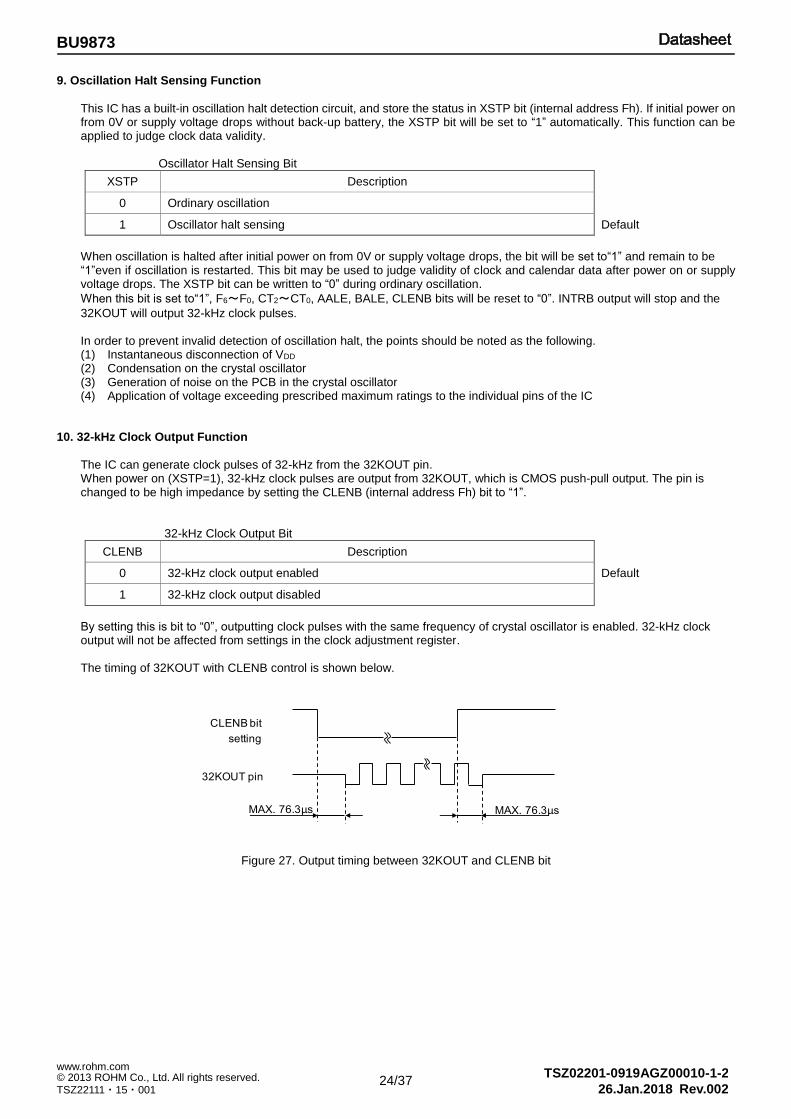
The IC can generate clock pulses of 32-kHz from the 32KOUT pin. When power on (XSTP=1), 32-kHz clock pulses are output from 32KOUT, which is CMOS push-pull output. The pin is changed to be high impedance by setting the CLENB (internal address Fh) bit to “1”.
32-kHz Clock Output Bit
CLENB Description
0 32-kHz clock output enabled Default
1 32-kHz clock output disabled
By setting this is bit to “0”, outputting clock pulses with the same frequency of crystal oscillator is enabled. 32-kHz clock output will not be affected from settings in the clock adjustment register. The timing of 32KOUT with CLENB control is shown below.
Figure 27. Output timing between 32KOUT and CLENB bit
Typical frequency of quartz crystal is 32.768 kHz. Generally, quartz crystal units have basic characteristics including an equivalent series resistance (R1) indicating the oscillation margin and a load capacitance (CL) indicating the degree of their center frequency. We recommended characteristics of crystal units for the BU9873 as follows:
(1) Max. R1 is up to 80kΩ. (2) CL value of 6 to 12.5pF.
The stability of quartz crystal units' oscillation depends on the parasitic capacitance of the circuit board and external oscillator capacitors (CGout and CDout). The best CL value we recommended is 6 to 8pF, but if CL value is more than 8pF, please use the oscillation adjustment method and refer to P17 “Oscillation Adjustment Function with Digital Method”.
Install the quartz crystal unit in the closest position to the real-time clock ICs. Avoid using any long parallel lines to wire the OSCIN and OSCOUT pins. Avoid laying any signal lines or power lines in the vicinity of the oscillation circuit.
2. Pull Up Resistor RPU
(1) Pull up resistance of SDA and INTRB terminal SDA and INTRB output is NMOS open drain, so requires pull up resistance. As for this resistance value (RPU), select an appropriate value from microcontroller VIL, IL, and VOL-IOL characteristics of this IC. If RPU is large, operating frequency is limited. The smaller the RPU, the larger is the consumption current.
(a) Maximum value of RPU
The maximum value of RPU is determined by the following factors.
• SDA rise time to be determined by the capacitance (CBUS) of bus line of RPU and SDA should be tR or lower. And
AC timing should be satisfied even when SDA rise time is slow.
• The bus electric potential ○A to be determined by input leak total (IL) of device connected to bus at output of 'H'
to the SDA line and RPU should sufficiently secure the input 'H' level (VIH) of microcontroller and RTC including
recommended noise margin 0.2Vcc.
IHCCPULCC V V 0.2RIV ≥--
L
IHCCPU
I
VVR
-8.0∴
Ex.) Vcc =3V IL=10µA VIH=0.7 Vcc
thus
6PU1010
370380R -
-∴
×
×.×.≤
][≤ Ωk30
(b) Minimum value of RPU
The minimum value of RPU is determined by the following factors.
• When IC outputs LOW, it should be satisfied that VOLMAX=0.4V and IOLMAX=1mA.
Therefore, the second condition is also satisfied.
(2) Pull up resistance of SCL terminal
When SCL control is made at CMOS output port, there is no need for a pull up resistor. But when there is timing where SCL becomes 'Hi-Z', add a pull up resistance. As for the pull up resistor value, one of several kΩ to several ten kΩ is recommended in consideration of drive performance of output port of microcontroller.
3. Bypass Capacitor C1 and C2
When noise or surge gets in the power source line, malfunction may occur, therefore, for removing these, it is recommended to attach bypass capacitors between IC VDD and GND. Set bypass capacitors as close as possible to the IC, use a capacitor for high frequency and another capacitor for low frequency in parallel. Recommended value for big capacitor C2 is 0.1µF, and small capacitor C1 is several pF to hundreds of pF depending on the real application. And, it is also recommended to attach a bypass capacitor between board VDD and GND.
Connecting the power supply in reverse polarity can damage the IC. Take precautions against reverse polarity when connecting the power supply, such as mounting an external diode between the power supply and the IC’s power supply terminals.
2. Power Supply Lines
Design the PCB layout pattern to provide low impedance supply lines. Separate the ground and supply lines of the digital and analog blocks to prevent noise in the ground and supply lines of the digital block from affecting the analog block. Furthermore, connect a capacitor to ground at all power supply pins. Consider the effect of temperature and aging on the capacitance value when using electrolytic capacitors.
3. Ground Voltage
Ensure that no pins are at a voltage below that of the ground pin at any time, even during transient condition.
4. Ground Wiring Pattern
When using both small-signal and large-current ground traces, the two ground traces should be routed separately but connected to a single ground at the reference point of the application board to avoid fluctuations in the small-signal ground caused by large currents. Also ensure that the ground traces of external components do not cause variations on the ground voltage. The ground lines must be as short and thick as possible to reduce line impedance.
5. Thermal Consideration
Should by any chance the power dissipation rating be exceeded, the rise in temperature of the chip may result in deterioration of the properties of the chip. The absolute maximum rating of the Pd stated in this specification is when the IC is mounted on a 70mm x 70mm x 1.6mm glass epoxy board. In case of exceeding this absolute maximum rating, increase the board size and copper area to prevent exceeding the Pd rating.
6. Operating Conditions
These conditions represent a range within which the expected characteristics of the IC can be approximately obtained. The electrical characteristics are guaranteed under the conditions of each parameter.
7. Rush Current
When power is first supplied to the IC, it is possible that the internal logic may be unstable and inrush current may flow instantaneously due to the internal powering sequence and delays, especially if the IC has more than one power supply. Therefore, give special consideration to power coupling capacitance, power wiring, width of ground wiring, and routing of connections.
8. Operation Under Strong Electromagnetic Field
Operating the IC in the presence of a strong electromagnetic field may cause the IC to malfunction.
9. Testing on Application Boards
When testing the IC on an application board, connecting a capacitor directly to a low-impedance output pin may subject the IC to stress. Always discharge capacitors completely after each process or step. The IC’s power supply should always be turned off completely before connecting or removing it from the test setup during the inspection process. To prevent damage from static discharge, ground the IC during assembly and use similar precautions during transport and storage.
10. Inter-pin Short and Mounting Errors
Ensure that the direction and position are correct when mounting the IC on the PCB. Incorrect mounting may result in damaging the IC. Avoid nearby pins being shorted to each other especially to ground, power supply and output pin. Inter-pin shorts could be due to many reasons such as metal particles, water droplets (in very humid environment) and unintentional solder bridge deposited in between pins during assembly to name a few.
11. Unused Input Terminals
Input terminals of an IC are often connected to the gate of a MOS transistor. The gate has extremely high impedance and extremely low capacitance. If left unconnected, the electric field from the outside can easily charge it. The small charge acquired in this way is enough to produce a significant effect on the conduction through the transistor and cause unexpected operation of the IC. So unless otherwise specified, unused input terminals should be connected to the power supply or ground line.
12. Regarding Input Pins of the IC
In the construction of this IC, P-N junctions are inevitably formed creating parasitic diodes or transistors. The operation of these parasitic elements can result in mutual interference among circuits, operational faults, or physical damage. Therefore, conditions which cause these parasitic elements to operate, such as applying a voltage to an input pin lower than the ground voltage should be avoided. Furthermore, do not apply a voltage to the input terminals when no power supply voltage is applied to the IC. Even if the power supply voltage is applied, make sure that the input terminals have voltages within the values specified in the electrical characteristics of this IC.
During power on, in IC internal circuit and set, VDD rises through unstable low voltage area, and IC inside is not completely reset, and malfunction may occur. To prevent this, functions of POR circuit and LVDD circuit are equipped. To assure the action, observe the following conditions during power on.
(1) Set SDA = “H” and SCL =“L” or “H” (2) Start power source so as to satisfy conditions of tR, tOFF, and Vbot for operating POR circuit. If it is necessary, please use the discharge circuits of battery to satisfy its conditions.
P.1 “Control Register” was updated. P.2 Typical application circuit was updated. P.4 “Recommend” was deleted from Operating Conditions. Tstg was updated. P.4 Figure 4 was updated. P.5 “L” Output Current was updated. P.6 (Note1) was updated. “Condition” was updated. P.16 “from 00 to 59” and “from 00 to 23” were updated.
P.17 (*, 0, 0, 0, 0, 0, *) was updated. “((/F5, /F4, /F3, /F2, /F1, /F0)+1) ×2” was updated.
P.18 Example of Calculations was updated. P.19 Usage of Alarm Interrupt Function’s table was updated. P.19 “12-hour system” was updated. P.20 “INTRB and AAFG (BAFG) bit” was updated. Figure 23 was updated. P.21 Figure 24 was updated. P.22 Figure 25 was updated. The inaccurate spelling and sentence were updated. P.24 Figure 27 was updated. P.25 “RTC” was updated. P.26 “RTC” was updated. P.28 “Recommend” was deleted from Operating Conditions. P.29 Notes during Power ON was updated. P.30 Packaging and Forming Specification was updated. Lineup was updated.
Precaution on using ROHM Products 1. Our Products are designed and manufactured for application in ordinary electronic equipment (such as AV equipment,
OA equipment, telecommunication equipment, home electronic appliances, amusement equipment, etc.). If you intend to use our Products in devices requiring extremely high reliability (such as medical equipment
(Note 1), transport
equipment, traffic equipment, aircraft/spacecraft, nuclear power controllers, fuel controllers, car equipment including car accessories, safety devices, etc.) and whose malfunction or failure may cause loss of human life, bodily injury or serious damage to property (“Specific Applications”), please consult with the ROHM sales representative in advance. Unless otherwise agreed in writing by ROHM in advance, ROHM shall not be in any way responsible or liable for any damages, expenses or losses incurred by you or third parties arising from the use of any ROHM’s Products for Specific Applications.
(Note1) Medical Equipment Classification of the Specific Applications
JAPAN USA EU CHINA
CLASSⅢ CLASSⅢ
CLASSⅡb CLASSⅢ
CLASSⅣ CLASSⅢ
2. ROHM designs and manufactures its Products subject to strict quality control system. However, semiconductor
products can fail or malfunction at a certain rate. Please be sure to implement, at your own responsibilities, adequate safety measures including but not limited to fail-safe design against the physical injury, damage to any property, which a failure or malfunction of our Products may cause. The following are examples of safety measures:
[a] Installation of protection circuits or other protective devices to improve system safety [b] Installation of redundant circuits to reduce the impact of single or multiple circuit failure
3. Our Products are designed and manufactured for use under standard conditions and not under any special or extraordinary environments or conditions, as exemplified below. Accordingly, ROHM shall not be in any way responsible or liable for any damages, expenses or losses arising from the use of any ROHM’s Products under any special or extraordinary environments or conditions. If you intend to use our Products under any special or extraordinary environments or conditions (as exemplified below), your independent verification and confirmation of product performance, reliability, etc, prior to use, must be necessary:
[a] Use of our Products in any types of liquid, including water, oils, chemicals, and organic solvents [b] Use of our Products outdoors or in places where the Products are exposed to direct sunlight or dust [c] Use of our Products in places where the Products are exposed to sea wind or corrosive gases, including Cl2,
H2S, NH3, SO2, and NO2
[d] Use of our Products in places where the Products are exposed to static electricity or electromagnetic waves [e] Use of our Products in proximity to heat-producing components, plastic cords, or other flammable items [f] Sealing or coating our Products with resin or other coating materials [g] Use of our Products without cleaning residue of flux (even if you use no-clean type fluxes, cleaning residue of
flux is recommended); or Washing our Products by using water or water-soluble cleaning agents for cleaning residue after soldering
[h] Use of the Products in places subject to dew condensation
4. The Products are not subject to radiation-proof design. 5. Please verify and confirm characteristics of the final or mounted products in using the Products. 6. In particular, if a transient load (a large amount of load applied in a short period of time, such as pulse. is applied,
confirmation of performance characteristics after on-board mounting is strongly recommended. Avoid applying power exceeding normal rated power; exceeding the power rating under steady-state loading condition may negatively affect product performance and reliability.
7. De-rate Power Dissipation depending on ambient temperature. When used in sealed area, confirm that it is the use in
the range that does not exceed the maximum junction temperature. 8. Confirm that operation temperature is within the specified range described in the product specification. 9. ROHM shall not be in any way responsible or liable for failure induced under deviant condition from what is defined in
this document.
Precaution for Mounting / Circuit board design 1. When a highly active halogenous (chlorine, bromine, etc.) flux is used, the residue of flux may negatively affect product
performance and reliability.
2. In principle, the reflow soldering method must be used on a surface-mount products, the flow soldering method must be used on a through hole mount products. If the flow soldering method is preferred on a surface-mount products, please consult with the ROHM representative in advance.
For details, please refer to ROHM Mounting specification
Precautions Regarding Application Examples and External Circuits 1. If change is made to the constant of an external circuit, please allow a sufficient margin considering variations of the
characteristics of the Products and external components, including transient characteristics, as well as static characteristics.
2. You agree that application notes, reference designs, and associated data and information contained in this document
are presented only as guidance for Products use. Therefore, in case you use such information, you are solely responsible for it and you must exercise your own independent verification and judgment in the use of such information contained in this document. ROHM shall not be in any way responsible or liable for any damages, expenses or losses incurred by you or third parties arising from the use of such information.
Precaution for Electrostatic This Product is electrostatic sensitive product, which may be damaged due to electrostatic discharge. Please take proper caution in your manufacturing process and storage so that voltage exceeding the Products maximum rating will not be applied to Products. Please take special care under dry condition (e.g. Grounding of human body / equipment / solder iron, isolation from charged objects, setting of Ionizer, friction prevention and temperature / humidity control).
Precaution for Storage / Transportation 1. Product performance and soldered connections may deteriorate if the Products are stored in the places where:
[a] the Products are exposed to sea winds or corrosive gases, including Cl2, H2S, NH3, SO2, and NO2 [b] the temperature or humidity exceeds those recommended by ROHM [c] the Products are exposed to direct sunshine or condensation [d] the Products are exposed to high Electrostatic
2. Even under ROHM recommended storage condition, solderability of products out of recommended storage time period may be degraded. It is strongly recommended to confirm solderability before using Products of which storage time is exceeding the recommended storage time period.
3. Store / transport cartons in the correct direction, which is indicated on a carton with a symbol. Otherwise bent leads
may occur due to excessive stress applied when dropping of a carton. 4. Use Products within the specified time after opening a humidity barrier bag. Baking is required before using Products of
which storage time is exceeding the recommended storage time period.
Precaution for Product Label A two-dimensional barcode printed on ROHM Products label is for ROHM’s internal use only.
Precaution for Disposition When disposing Products please dispose them properly using an authorized industry waste company.
Precaution for Foreign Exchange and Foreign Trade act Since concerned goods might be fallen under listed items of export control prescribed by Foreign exchange and Foreign trade act, please consult with ROHM in case of export.
Precaution Regarding Intellectual Property Rights 1. All information and data including but not limited to application example contained in this document is for reference
only. ROHM does not warrant that foregoing information or data will not infringe any intellectual property rights or any other rights of any third party regarding such information or data.
2. ROHM shall not have any obligations where the claims, actions or demands arising from the combination of the Products with other articles such as components, circuits, systems or external equipment (including software).
3. No license, expressly or implied, is granted hereby under any intellectual property rights or other rights of ROHM or any third parties with respect to the Products or the information contained in this document. Provided, however, that ROHM will not assert its intellectual property rights or other rights against you or your customers to the extent necessary to manufacture or sell products containing the Products, subject to the terms and conditions herein.
Other Precaution 1. This document may not be reprinted or reproduced, in whole or in part, without prior written consent of ROHM.
2. The Products may not be disassembled, converted, modified, reproduced or otherwise changed without prior written consent of ROHM.
3. In no event shall you use in any way whatsoever the Products and the related technical information contained in the Products or this document for any military purposes, including but not limited to, the development of mass-destruction weapons.
4. The proper names of companies or products described in this document are trademarks or registered trademarks of ROHM, its affiliated companies or third parties.
General Precaution 1. Before you use our Products, you are requested to carefully read this document and fully understand its contents.
ROHM shall not be in any way responsible or liable for failure, malfunction or accident arising from the use of any ROHM’s Products against warning, caution or note contained in this document.
2. All information contained in this document is current as of the issuing date and subject to change without any prior
notice. Before purchasing or using ROHM’s Products, please confirm the latest information with a ROHM sales representative.
3. The information contained in this document is provided on an “as is” basis and ROHM does not warrant that all
information contained in this document is accurate and/or error-free. ROHM shall not be in any way responsible or liable for any damages, expenses or losses incurred by you or third parties resulting from inaccuracy or errors of or concerning such information.