Raider ® GT Copper Interconnect El t h i lD iti S t Electrochemical Deposition System Uniform, Small Feature Fill March 16, 2011 External Use SILICON SYSTEMS GROUP External Use SILICON SYSTEMS GROUP
Transcript
Raider® GT Copper Interconnect El t h i l D iti S tElectrochemical Deposition SystemUniform, Small Feature Fill
March 16, 2011
External UseSILICON SYSTEMS GROUP External UseSILICON SYSTEMS GROUP
Silicon Systems Group Overview
#1 in the Wafer Fab Equipment (WFE) and advanced(WFE) and advanced packaging markets
I 2011 t t WFE In 2011, expect to grow WFE market share for the 3rd consecutive year y
Growth fueled by new product innovations alignedinnovations aligned to technology inflections
External UseSILICON SYSTEMS GROUP2
Source: Gartner, April 2010
Innovations Enable Inflections
Conforma™ Doping
Centris™ Etch Avenir™ RF PVD Ni
Avila™ CVD
Tetra X™
Aera3™
Silvia™ EtchDFinder™ Inspection
Avenir™ RF PVD Gate
Eterna™ FCVD
Raider™ GT
Mesa™ Etch InVia™ CVDCentinel™ PVD / ALDSiconi™ for Epi
Success of Business Combination with Applied Materialswith Applied Materials
Semitool Rapid Innovation of New Technology Rapid Innovation of New Technology Leadership in Electrochemical Deposition Raider Platform Flexibility and Productivity
Semitool Combined with Applied Materials World Class Manufacturing and Logistics World Class Manufacturing and Logistics Dynamic Integration Development and Demonstration with Maydan
Technology Center Market Leadership and Mutual Customer Trust and Respect Leverage of Applied Global Support Infrastructure and Expertise Fueled for Growth
External UseSILICON SYSTEMS GROUP External UseSILICON SYSTEMS GROUPSILICON SYSTEMS GROUP
Fueled for Growth
9
Raider Customer Traction in Copper Interconnect PlatingInterconnect Plating
2006 2010Acquisition
Customer Tool-of-Record Tool-of-Record
A
B c/ dry 3 new customer
penetrations andC
D
Logi
Foun
d
penetrations and tool-of-record wins all driven through better small feature fill
A
B
C
mor
y
21% estimated market share in 2010(source: Gartner Mar ‘11)
D
E
Mem
( )
External UseSILICON SYSTEMS GROUP10
F
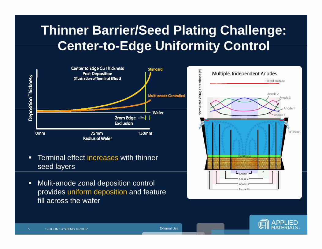
Applied Raider GT for Cu Electrochemical DepositionElectrochemical Deposition
Powerful Technology Superior Small Feature Fill Lowest Cost of Ownership
Innovation and Leadership Time to Market Technology Leading Integration Capability