4Raman Spectroscopy: from Graphite to sp2 Nanocarbons
This chapter gives a broad perspective on how Raman spectroscopy provides anespecially sensitive characterization tool for carbon-based materials and even moreso for sp2 nanocarbon materials. Since many other optical effects can also be uti-lized in probing sp2 carbons, to gain a clear understanding of the Raman scatteringprocess, we start by contextualizing the optical processes under the broad headingof light–matter interaction phenomena. We then briefly review a number of pho-tophysical phenomena in order to put the Raman effect into proper perspective(Sections 4.1 and 4.2). Following this discussion, we present the big picture of Ra-man spectra from sp2 carbon nanomaterials (Section 4.3). The atomic vibrationalnature of the modes related to each Raman peak is then introduced and the differ-ences in the observed Raman spectra for the different sp2 structures are addressed(Section 4.4). The presentation here is basic and follows a historic perspective, aim-ing to give the reader a broad picture of the Raman spectra from bulk graphite tosp2 nanocarbons. In Chapters 5 and 6 we discuss the quantum description and se-lection rules for the Raman scattering process, respectively. In Part Two of the bookwe elaborate on the science of each Raman mode that is introduced in the presentchapter, showing the great deal of information one can obtain from each of theseRaman features for each specific sp2 carbon system.
4.1Light Absorption
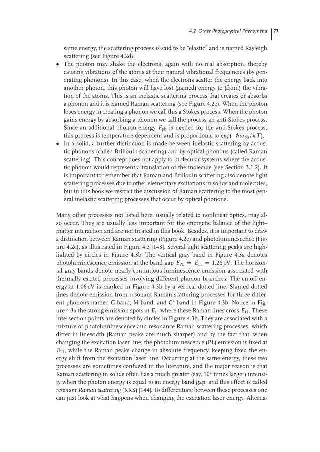
When shining light into a material (molecule or solid), part of the energy simplypasses through the sample (by transmission), while the remaining photons interactwith the system through light absorption, reflection, photoluminescence or lightscattering. The amount of light that will be transmitted, as well as the details for allthe light–matter interactions will be determined by the electronic and vibrationalproperties of the material. Furthermore, different phenomena occur when shininglight into a given material with different energy photons [1, 142], because differentenergies will be related to the different optical transitions occurring in the medium.As an example of the richness of light–matter interactions, a schematic opticalabsorption curve for a semiconducting material is shown in Figure 4.1. Using this
74 4 Raman Spectroscopy: from Graphite to sp2 Nanocarbons
Figure 4.1 Photophysical mechanisms operative for various regions of the electromagneticspectrum as photons in various energy ranges interact with materials.
figure as a guide, examples are given for the many different effects that might occurwhen light interacts with a material.
Starting from the high energy side of Figure 4.1:
� The photon (1–5 eV) can be absorbed by an electron making a transition fromthe valence band to the conduction band. Such a transition generates a freeelectron in the conduction band leaving behind a “hole” in the valence band,using the nomenclature of semiconductor physics.
� The photon with an energy smaller than the energy gap can generate an excitonlevel, which corresponds to an electron bound to a hole through the Coulombinteraction. Whereas excitonic levels in model semiconductor systems have ex-citonic levels of a few millielectron volts below the band gap, the energies incarbon nanotubes are much deeper (on the order of a few hundred millielec-tron volt range).
� If the semiconductor crystal contains impurities (foreign atoms), new energylevels appear in the energy band gap for an electron bound to such an impurityatom. If the impurity atom has more valence electrons than the atom it replaces,the impurity will act as an electron donor. If it has fewer electrons it will bean electron acceptor. Light can be absorbed, generating electronic transitionsfrom the valence band to the donor impurity levels, or taking electrons from theacceptor level to the conduction band. The corresponding photon energy is 10to 100 meV smaller than the energy gap.
4.2 Other Photophysical Phenomena 75
� When the photon energy coincides with the energy of optical phonons (10 meVto 0.2 eV for first-order processes), light will be absorbed, thereby creatingphonons. Harmonics and combination modes are observed also, extending thephoton energy range to � 350 meV. These processes occur in the infrared en-ergy range (infrared absorption), and play a major role in the field of infraredspectroscopy.
� Shallow donor level transitions to the conduction band and valence band transi-tions to shallow acceptor levels can also be responsible for light absorption. Thecorresponding photon energy would be significantly lower than the stronger ex-citations from the dominant bright state. In some cases the lowest state is a darkstate, which means it cannot be created by light absorption.
� The free carriers, which are electrons in metallic systems, and electrons and/orholes in doped semiconducting systems, can also absorb light, usually occur-ring over a broad energy range from 1 to 10 meV. Other free carrier processesnot shown in the diagram also occur. In a much higher energy region (1 to20 eV), the collective excitation of electrons also occurs. This is known as plas-mon absorption.For the much higher energy region of ultraviolet and X-ray electron excitation(not shown in Figure 4.1), transitions from core levels also occur. In this casewe observe the photoexcited electrons using experimental techniques knownas ultra-violet photoelectron spectroscopy (UPS) and X-ray photoelectron spec-troscopy (XPS).
One important aspect of optical absorption by crystals is related to wave vector orcrystal momentum conservation. In the visible range, the wavelength of light is onthe order of λlight � 500 nm. The dimensions of the Brillouin zones are defined bythe maximum value of the wave vector k, which is usually given by kBZ D π/a (seeSection 2.1.5), where the primitive translation vector a in the unit cell is about 0.1to 0.2 nm. Therefore, the photon wave vector is related to the maximum dimensionof the Brillouin zone (kBZ) by
klight D 2πλlight
� kBZ
3000. (4.1)
Since klight � kBZ, we say that a photon excites one electron from the valence bandto the conduction band with the same k. The transition is vertical in the electronenergy dispersion, that is, there is no change of wave vector in the electronic energydispersion.
4.2Other Photophysical Phenomena
Section 4.1 describes schematically various mechanisms that are responsible forthe optical absorption of light in a semiconducting material, as displayed in Fig-
76 4 Raman Spectroscopy: from Graphite to sp2 Nanocarbons
Figure 4.2 The light–matter interaction, show-ing the most commonly occurring processes.The waved arrows indicate incident and scat-tered photons. The vertical arrows denote thelight-induced transitions between (a) vibra-tional levels (see Figure 3.2) and (b–e) elec-tronic states. Curved arrow segments indicateelectron–phonon (hole–phonon) scatteringevents. In (e) the shortest vertical arrow alsoindicates an electron–phonon transition in Ra-
man scattering. In (d) and (e) the processeswill be resonant if the incident (or scattered)light energy exactly matches the energy dif-ference between initial and excited electronicstates. When far from the resonance win-dow where resonance occurs, the transitionis called virtual. The intensity for resonanceRaman scattering can be much larger for thevertical processes.
ure 4.1. Now we broadly discuss different phenomena occurring via light–matterinteractions (see Figure 4.2):
� The photon energy that has been absorbed can in one case be transformed intoatomic vibrations, that is, heat. When the light energy matches the energy forallowed phonon transitions, the photon can transfer energy directly to create anacoustic or optical phonon (see Figure 4.2a). This resonance process is calledinfrared (IR) absorption, since phonon energies occur at infrared frequencies.
� Even if the photon energy does not match the energy of the optical phonons,this photon energy can be transferred to the electrons. The photoexcited elec-trons then lose energy by creating multiple phonons of different frequencies byelectron–phonon coupling. In a metal, such photoexcited electrons will decaydown to their ground states through electron–phonon coupling in a process asshown in Figure 4.2b. If the material has an energy gap between the occupied(valence) and unoccupied (conduction) bands, the photoexcited electron can de-cay first to the bottom of the conduction band by an electron–phonon processand then to its ground state by emitting a photon with the band gap energy, (seeFigure 4.2c). This process is called photoluminescence.
� A photon may be virtually absorbed by a material (not real absorption), whichmeans the photon (oscillating electric field) just shakes the electrons, which willthen scatter that energy back to another photon with the same energy as theincident one. In the case where the incident and scattered photons have the
4.2 Other Photophysical Phenomena 77
same energy, the scattering process is said to be “elastic” and is named Rayleighscattering (see Figure 4.2d).
� The photon may shake the electrons, again with no real absorption, therebycausing vibrations of the atoms at their natural vibrational frequencies (by gen-erating phonons). In this case, when the electrons scatter the energy back intoanother photon, this photon will have lost (gained) energy to (from) the vibra-tion of the atoms. This is an inelastic scattering process that creates or absorbsa phonon and it is named Raman scattering (see Figure 4.2e). When the photonloses energy in creating a phonon we call this a Stokes process. When the photongains energy by absorbing a phonon we call the process an anti-Stokes process.Since an additional phonon energy Eph is needed for the anti-Stokes process,this process is temperature-dependent and is proportional to exp(�„ωph/ k T ).
� In a solid, a further distinction is made between inelastic scattering by acous-tic phonons (called Brillouin scattering) and by optical phonons (called Ramanscattering). This concept does not apply to molecular systems where the acous-tic phonon would represent a translation of the molecule (see Section 3.1.2). Itis important to remember that Raman and Brillouin scattering also denote lightscattering processes due to other elementary excitations in solids and molecules,but in this book we restrict the discussion of Raman scattering to the most gen-eral inelastic scattering processes that occur by optical phonons.
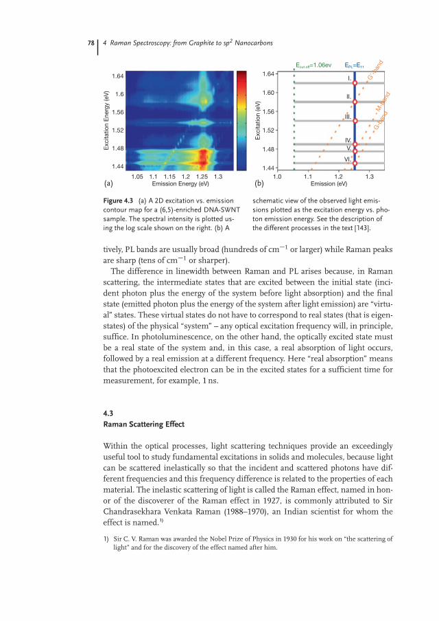
Many other processes not listed here, usually related to nonlinear optics, may al-so occur. They are usually less important for the energetic balance of the light–matter interaction and are not treated in this book. Besides, it is important to drawa distinction between Raman scattering (Figure 4.2e) and photoluminescence (Fig-ure 4.2c), as illustrated in Figure 4.3 [143]. Several light scattering peaks are high-lighted by circles in Figure 4.3b. The vertical gray band in Figure 4.3a denotesphotoluminescence emission at the band gap EPL D E11 D 1.26 eV. The horizon-tal gray bands denote nearly continuous luminescence emission associated withthermally excited processes involving different phonon branches. The cutoff en-ergy at 1.06 eV is marked in Figure 4.3b by a vertical dotted line. Slanted dottedlines denote emission from resonant Raman scattering processes for three differ-ent phonons named G-band, M-band, and G0-band in Figure 4.3b. Notice in Fig-ure 4.3a the strong emission spots at E11 where these Raman lines cross E11. Theseintersection points are denoted by circles in Figure 4.3b. They are associated with amixture of photoluminescence and resonance Raman scattering processes, whichdiffer in linewidth (Raman peaks are much sharper) and by the fact that, whenchanging the excitation laser line, the photoluminescence (PL) emission is fixed atE11, while the Raman peaks change in absolute frequency, keeping fixed the en-ergy shift from the excitation laser line. Occurring at the same energy, these twoprocesses are sometimes confused in the literature, and the major reason is thatRaman scattering in solids often has a much greater (say, 103 times larger) intensi-ty when the photon energy is equal to an energy band gap, and this effect is calledresonant Raman scattering (RRS) [144]. To differentiate between these processes onecan just look at what happens when changing the excitation laser energy. Alterna-
78 4 Raman Spectroscopy: from Graphite to sp2 Nanocarbons
1.01.05
1.44
(a) (b)
1.48
1.52
1.56
1.6
1.64
1.1 1.15 1.2 1.25 1.3Emission (eV)Emission Energy (eV)
Exc
itatio
n (e
V)
Exc
itatio
n E
nerg
y (e
V)
1.44
1.48
1.52
1.56
1.60
1.64
Ecut off=1.06ev EPL=E11
G'-b
and
M-b
and
G-b
and
1.1 1.2 1.3
I.
II.
III.
IV.V.
VI.
Figure 4.3 (a) A 2D excitation vs. emissioncontour map for a (6,5)-enriched DNA-SWNTsample. The spectral intensity is plotted us-ing the log scale shown on the right. (b) A
schematic view of the observed light emis-sions plotted as the excitation energy vs. pho-ton emission energy. See the description ofthe different processes in the text [143].
tively, PL bands are usually broad (hundreds of cm�1 or larger) while Raman peaksare sharp (tens of cm�1 or sharper).
The difference in linewidth between Raman and PL arises because, in Ramanscattering, the intermediate states that are excited between the initial state (inci-dent photon plus the energy of the system before light absorption) and the finalstate (emitted photon plus the energy of the system after light emission) are “virtu-al” states. These virtual states do not have to correspond to real states (that is eigen-states) of the physical “system” – any optical excitation frequency will, in principle,suffice. In photoluminescence, on the other hand, the optically excited state mustbe a real state of the system and, in this case, a real absorption of light occurs,followed by a real emission at a different frequency. Here “real absorption” meansthat the photoexcited electron can be in the excited states for a sufficient time formeasurement, for example, 1 ns.
4.3Raman Scattering Effect
Within the optical processes, light scattering techniques provide an exceedinglyuseful tool to study fundamental excitations in solids and molecules, because lightcan be scattered inelastically so that the incident and scattered photons have dif-ferent frequencies and this frequency difference is related to the properties of eachmaterial. The inelastic scattering of light is called the Raman effect, named in hon-or of the discoverer of the Raman effect in 1927, is commonly attributed to SirChandrasekhara Venkata Raman (1988–1970), an Indian scientist for whom theeffect is named.1)
1) Sir C. V. Raman was awarded the Nobel Prize of Physics in 1930 for his work on “the scattering oflight” and for the discovery of the effect named after him.
4.3 Raman Scattering Effect 79
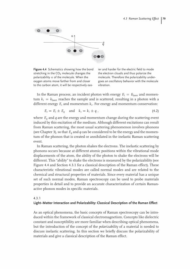
α
q
Figure 4.4 Schematics showing how the bondstretching in the CO2 molecule changes thepolarizability α of the molecule. When theoxygen atoms move farther from and closerto the carbon atom, it will be respectively eas-
ier and harder for the electric field to modethe electron clouds and thus polarize themolecule. Therefore the polarizability under-goes an oscillatory behavior with the moleculevibration.
In the Raman process, an incident photon with energy Ei D Elaser and momen-tum ki D klaser reaches the sample and is scattered, resulting in a photon with adifferent energy Es and momentum ks . For energy and momentum conservation:
Es D Ei ˙ Eq and ks D ki ˙ q , (4.2)
where Eq and q are the energy and momentum change during the scattering eventinduced by this excitation of the medium. Although different excitations can resultfrom Raman scattering, the most usual scattering phenomenon involves phonons(see Chapter 3), so that Eq and q can be considered to be the energy and the momen-tum of the phonon that is created or annihilated in the inelastic Raman scatteringevent.
In Raman scattering, the photon shakes the electrons. The inelastic scattering byphonons occurs because at different atomic positions within the vibrational modedisplacements of the atom, the ability of the photon to shake the electrons will bedifferent. This “ability” to shake the electrons is measured by the polarizability (seeFigure 4.4 and Section 4.3.1 for a classical description of the Raman effect). Thesecharacteristic vibrational modes are called normal modes and are related to thechemical and structural properties of materials. Since every material has a uniqueset of such normal modes, Raman spectroscopy can be used to probe materialsproperties in detail and to provide an accurate characterization of certain Raman-active phonon modes in specific materials.
4.3.1Light–Matter Interaction and Polarizability: Classical Description of the Raman Effect
As an optical phenomena, the basic concepts of Raman spectroscopy can be intro-duced within the framework of classical electromagnetism. Concepts like dielectricconstant and susceptibility are more familiar when describing optical phenomena,but the introduction of the concept of the polarizability of a material is needed todiscuss inelastic scattering. In this section we briefly discuss the polarizability ofmaterials and give a classical description of the Raman effect.
80 4 Raman Spectroscopy: from Graphite to sp2 Nanocarbons
In describing the polarizability α of an atom in a material, we start by defining αin terms of the polarization vector of the atom p and the local electric field Elocal atthe position of the atom:
p D αElocal . (4.3)
The polarizability α is an atomic property, and the dielectric constant � of a materialwill depend on the manner in which the atoms are assembled to form a crystal. Fora nonspherical atom, α is described by a tensor.2) The polarization P of a crystal orof a molecule may be approximated by summing the product of the polarizabilityof the individual atoms in the crystal (or of the molecule) times the local electricfields
P DX
j
N j p j DX
j
N j α j Elocal( j ) , (4.4)
where N j is the atomic concentration of each species and we sum over all theatoms in the crystal using the atomic polarization p j given by Eq. (4.3). If the localfield Elocal( j ) is given by the Lorentz relation Elocal( j ) D E C (4π/3)P , then weobtain
P DX
j
N j α j
�E C 4π
3P
�. (4.5)
Solving for the susceptibility � we then obtain
� � P
ED
Pj N j α j
1 � 4π3
Pj N j α j
. (4.6)
Using the definition for the dielectric constant � which relates the displacementvector D to the electric field E through the relation � D 1 C 4π�, one obtains theClausius–Mossotti relation
� � 1� C 2
D 4π3
Xj
N j α j , (4.7)
which relates the dielectric constant � to the electronic polarizability α, but only forcrystal structures for which the Lorentz local field relation applies.
Light scattering can then be understood simply on the basis of classical electro-magnetic theory. When an electric field E is applied to a solid, a polarization Presults
P D$α �E , (4.8)
2) In this case, the second-rank tensor α isa 3 � 3 matrix. When we consider p andElocal using another coordinate system,each component of the p and Elocal vectorsis transformed by a unitary matrix U,representing rotation, inversion, etc., such asU p and U Elocal. Then α is transformed bythe unitary transformation U αU�1, which
preserves length scales. A matrix whichtransforms as U αU�1 for a transformationof coordinates is defined as a second-ranktensor. p and Elocal are both vectors and arecalled first-rank tensors since U appears onceunder a coordinate or more general unitarytransformation.
4.3 Raman Scattering Effect 81
where$α is the polarizability tensor of the atom in the solid, indicating that positive
charge moves in one direction and negative charge moves in the opposite directionunder the influence of the applied field. We now use these results to obtain a clas-sical description for the Raman effect.
In light scattering experiments, the electric field of the light is oscillating at anoptical frequency ω i
E D E0 sin ω i t . (4.9)
The lattice vibrations in the solid with a frequency ωq modulate the polarizabilityof the atoms α, where
α D α0 C α1 sin ωq t , (4.10)
and ωq is a normal mode frequency of the solid that couples to the optical field sothat the polarization which is induced by the applied electric field becomes:
P D E0(α0 C α1 sin ωq t) sin ω0 t
D E0
�α0 sin(ω i t) C 1
2α1 cos(ω i � ωq)t � 1
2α1 cos(ω i C ωq)t
�. (4.11)
Thus, we see from Eq. (4.11) that light will be scattered both elastically at a frequen-cy ω i (Rayleigh scattering) and also inelastically, being downshifted by the naturalvibration frequency ωq of the atom (i. e., by the Stokes process for the emission ofa phonon) or upshifted by the same frequency ωq (by the anti-Stokes process forthe absorption of a phonon). For a good appreciation of α1, it is necessary to intro-duce quantum theory, and this is the subject of Chapter 5. In the present chapterwe simply introduce the basic concept of Raman spectroscopy. In Section 4.3.2, wedescribe its general characteristics.
4.3.2Characteristics of the Raman Effect
In this section we very briefly summarize a number of the important characteristicsof the Raman Effect that will be broadly used throughout this book.
4.3.2.1 Stokes and Anti-Stokes Raman ProcessesIn the inelastic scattering process, the incident photon can decrease or increase itsenergy by creating (Stokes process) or destroying (anti-Stokes process) a phononexcitation in the medium. The plus (minus) signs in Eqs. (4.2) and inside paren-thesis in Eq. (4.11) apply when energy has been received from (transferred to) themedium excited by the Raman signal. The probability for the two types of eventsdepends on the excitation photon energy Ei in the scattered photon energy Es andon the temperature.
The probability to annihilate or create a phonon depends on the phonon statis-tics, which is given by the Bose–Einstein distribution function. At a given temper-ature, the average number of phonons n with energy Eq is given by:
n D 1eEq/ kB T � 1
, (4.12)
82 4 Raman Spectroscopy: from Graphite to sp2 Nanocarbons
where kB is the Boltzmann constant and T is the temperature. Since the vibrationalenergy Eq of the harmonic oscillator with n phonons is given by Eq(n C 1/2), con-sequently the scattering event for having n phonons depends on the temperature.The probability for the Stokes (S) and anti-Stokes (aS) processes differs because inthe Stokes process the system goes from n phonons to n C 1, while in the anti-Stokes process the opposite occurs. Using time reversal symmetry, the matrix ele-ments for the transition n ! n C 1 (Stokes) and n C 1 ! n (anti-Stokes) are thesame, and the intensity ratio between the Stokes and anti-Stokes signals from onegiven phonon can be obtained by
IS
IaS/ n C 1
nD eEq/ kB T , (4.13)
where IS and IaS denote the measured intensity for the Stokes and anti-Stokespeaks, respectively.
Since Eq. (4.13) is obtained through time reversal symmetry, this relation shouldbe applicable only when the Stokes and anti-Stokes processes are measured usingdifferent incident photon energies (different Elaser), that is, when the incident ener-gy for the Stokes process matches the scattered energy for the anti-Stokes process(time reversal). However, usually this is not important, since the phonon energyis much smaller than the laser energy, so that incident and scattered energies arevery close to each other. The previous assumption does not hold when resonanceRaman scattering with sharp energy levels takes place. In this case, strong devia-tions from Eq. (4.13) can be obtained if IS and IaS are taken with the same Elaser.The resonance condition might not occur at the same Elaser for S and aS Ramanscattering.
Finally, because the anti-Stokes signal is usually weaker than the Stokes process,it is usual that people only care about the Stokes spectra. Therefore, in this book,when not referring explicitly to the type of scattering process, it is the Stokes pro-cess that is being addressed.
4.3.2.2 The Raman SpectrumA Raman spectrum is a plot of the scattered intensity Is as a function of Elaser �Es (Raman shift, see Figure 4.5), and the energy conservation relation given byEq. (4.2) is a very important aspect of Raman spectroscopy. The Raman spectrawill show peaks at a phonon energy ˙Eq , where Eq is the energy of the excitationassociated with the Raman effect. By convention, the energy of the Stokes processoccurs at positive energy while the anti-Stokes process occurs at a negative energy.Thus, in the spectrometer (grating) which divides the scattered light into differentdirections, the anti-Stokes signal appears in the opposite position relative to theStokes signal with respect to the central Rayleigh signal.
4.3.2.3 Raman Lineshape and Raman Spectral Linewidth Γq
The Raman spectrum exhibits a peak at Elaser � Es D Eq where the phonon exci-tation can be represented by a harmonic oscillator damped by the interaction withother excitations in the medium (similar to a mass-spring system inside a liquid).
4.3 Raman Scattering Effect 83
Figure 4.5 Schematics showing the Rayleigh(at 0 cm�1) and the Raman spectrum. TheRayleigh intensity is always much strongerand it has to be filtered out for any mean-ingful Raman experiment. The Stokes pro-
cesses (positive frequency peaks) are usu-ally stronger than the anti-Stokes processes(negative frequency peaks) due to phononcreation/annihilation statistics.
Therefore, the shape of the Raman peak will be the response of a damped har-monic oscillator with eigenfrequency ωq that is forced by an external field with afrequency ω. Considering the damping energy given by Γq , the power dissipatedby a forced damped harmonic oscillator is a Lorentzian curve
I(ω) D I0
πΓq
1(ω � ωq)2 C Γ 2
q
, (4.14)
in the limit where the frequency ωq � Γq .3) The full width at half maximum in-tensity is given by FWHM = 2Γq . The center of the Lorentzian gives the naturalvibration frequency ωq , and Γq is related to the damping or the energy uncertaintyor the lifetime of the phonon [145]. Therefore, when the damping of the amplitudeoccurs as the scattered light energy is varied, as characterized by Γq, the corre-sponding phonon has a finite life time, ∆ t. The uncertainty principle ∆E∆ t � „gives an uncertainty in the value of the phonon energy, as measured in the Ra-man spectrum, which corresponds to the spectral FWHM of 2Γq . Therefore, Γq isthe inverse of the lifetime for a phonon, and Raman spectra in this way provideinformation on phonon lifetimes.
There are two main reasons for the finite phonon lifetime:
� Anharmonicity of the potential for the phonon so that, for large q far from thepotential minimum, qeq is no longer a good quantum number and phonon scat-tering occurs by emitting a phonon (third-order process) or by phonon–phonon
3) The solution of a forced damped harmonic oscillator is not a Lorentzian. It approaches theLorentzian function for ωq � Γq . If ωq approaches Γq , the lineshape departs from a Lorentzianshape.
84 4 Raman Spectroscopy: from Graphite to sp2 Nanocarbons
scattering (fourth-order anharmonicity). Anharmonicity is a main contributionto the thermal expansion (third-order process) and to the thermal conductivity(fourth-order process).
� Another possible interaction is the electron–phonon interaction in which aphonon excites an electron in the valence band to the conduction band orscatters a photoexcited electron to other unoccupied states. The former elec-tron–phonon process works for electrons in the valence band while the latterelectron–phonon process associated with anharmonicity works for electronsin excited states. Thus the origin of these two electron–phonon processes aredifferent from each other.
In specific cases, the Raman feature can deviate from the simple Lorentzian shape.One obvious case is when the feature is actually composed of more than onephonon contribution. Then the Raman peak will be a convolution of severalLorentzian peaks, depending on the weight of each phonon contribution. An-other case is when the lattice vibration couples to electrons, that is, when theelectron–phonon interaction takes place. In this case, additional line broadeningand even distorted (asymmetric) lineshapes can result and this effect is known asthe Kohn anomaly. In cases where phonons are coupled to electrons, the Ramanpeak may exhibit a so-called Breit–Wigner–Fano (BWF) lineshape, given by [147]:
I(ω) D I0[1 C (ω � ωBWF/qBWF ΓBWF)]2
1 C [(ω � ωBWF/ΓBWF)]2, (4.15)
where 1/qBWF is a measure of the interaction of a discrete level (the phonon) witha continuum of states (the electrons), ωBWF is the BWF peak frequency at maxi-mum intensity I0, and ΓBWF is the half width of the BWF peak. Such effects areobserved in certain metallic sp2 carbon materials and are discussed in Chapter 8,in connection with metallic carbon nanotubes.
4.3.2.4 Energy Units: cm�1
The energy axis in the Raman spectra is usually displayed in units of cm�1. 1 cm�1
is the energy of a photom whose wavelength is 2π cm. Lasers are usually describedby the wavelength of the light, that is, in nanometers, but the phonon energies areusually too small a number when displayed in nanometers, and the Raman shiftsare thus given in units of cm�1 (1 cm�1 is equivalent to 10�7 nm�1). Furthermore,the accuracy of a common Raman spectrometer is on the order of 1 cm�1. It isimportant to note that the wave number is expressed in units of cm�1 but thedefinition of the wavenumber in this case is k D 1/λ (where λ is the wavelengthof light) which is different from the definition of the wavenumber in solid statephysics, k D 2π/λ. The energy conversion factors are: 1 eV D 8065.5 cm�1 D2.418 1014 Hz D 11 600 K. Also 1 eV corresponds to a wavelength of 1.2398 µm.
4.3 Raman Scattering Effect 85
4.3.2.5 Resonance Raman Scattering and Resonance Window Linewidth γr
The laser excitation energies are usually much higher than the phonon energies.Therefore, although the exchange in energy between light and the medium is trans-ferred to the atomic vibrations, the light–matter interaction is mediated by elec-trons. Usually the photon energy is not large enough to achieve a real electronictransition, and the electron that absorbs the light is said to be excited to a “virtualstate”, from where it couples to the lattice, generating the Raman scattering pro-cess. However, when the excitation laser energy Elaser matches the actual energygap between the valence and conduction bands Eg in a semiconducting medium(or between an occupied initial state and an unoccupied final state more generally),the probability for the scattering event to occur increases by many orders of mag-nitude (� 103), and the process is then called a resonance Raman process (non-resonant otherwise). The same happens if the scattered light (Elaser ˙ Eq, where“C” denotes the anti-Stokes and “�” denotes the Stokes process) is equal to theelectronic transition Eg . Therefore, by varying Elaser through a discrete level Eg , theRaman intensity should increase when Elaser ! Eg (resonance with incident light)and when Elaser ! Eg ˙ Eq (resonance with scattered light). A plot of the Ramanintensity vs. Elaser gives the Raman excitation profile, according to
I(Elaser) Dˇ̌̌ˇ A
(Elaser � Eg � i γr)(Elaser � (Eg ˙ Eq) � i γr)
ˇ̌̌ˇ2
. (4.16)
The FWHM of each peak in such a plot of the Raman excitation profile is theresonance window width γr , and is related to the lifetime of the excited states, thatis, the lifetime for the Raman scattering process, which is the time delay betweenabsorption of the incoming photon and emission of the outgoing photon. In otherwords, γr is the inverse of the lifetime for the photoexcited carrier. The photoexcit-ed carrier can be relaxed from the excited states by
� The electron–phonon interaction for all possible phonons (with lifetimes< 1 ps);
� The electron–photon interaction (with lifetimes < 1 ns);� Other excitations such as the Auger process (Coulomb interaction) (lifetime
range not known yet for sp2 carbon).
Thus the electron–phonon interaction from k (a photoexcited state) to the energy-momentum conserved k C q (phonon emitting electron state) is dominant. Noticeγr (resonance window width) is different from the Γq (width on the Raman inten-sity vs. scattered light energy Raman spectrum, where Γq is related to the phononlifetime, see Section 4.3.2.3). These two experimental widths may be related or not,depending on the electron–phonon coupling. The physics behind the connectionbetween these widths is further discussed in Part Two of this book.The resonance effect is extremely important in nano-scale systems, since the Ra-man signal from nanomaterials is generally very weak because of the very smallsample size. Thus the large resonance enhancement by the resonance Raman ef-fect allows the observation of measurable Raman signals from nanostructures.
86 4 Raman Spectroscopy: from Graphite to sp2 Nanocarbons
For example, the large enhancement associated with the resonance Raman scat-tering (RRS) process provides a means to study the Raman spectrum from a singlegraphene sheet, a single graphene ribbon or an individual carbon nanotube, asdiscussed further in Section 4.4.
4.3.2.6 Momentum Conservation and Backscattering Configuration of LightAs discussed in this section, the q vector of the phonon carries information aboutthe wavelength of the vibration (q D 2π/λ) and the direction along which theoscillation occurs. In an inelastic scattering process, momentum conservation isrequired as given by Eq. (4.2). Different scattering geometries of light are possibleby the appropriate placement of the detector of the scattered light relative to thedirection of the incident light. If we select a specific choice of this geometry, wecan select different phonons due to the anisotropy of the scattering event by theselection rules for Raman scattering.
In a general scattering geometry in which the scattered light wave vector k s
makes an angle φ with the incident k i , the modulus of the phonon wave vector q
will be given by the law of cosines:
q2 D k2i C k2
s ˙ 2ki ks cos φ . (4.17)
The backscattering configuration of the light, for which ki and ks for the incidentand scattered light, respectively, have the same direction and opposite signs, givesthe largest possible q vector and is the most common scattering geometry whenworking with nanomaterials, because a microscope is usually needed to focus theincident light onto small samples and the scattered light is also collected by thesame microscope.
For the Raman-allowed one-phonon scattering process, the momentum transferis usually neglected, that is, ks � ki D q � 0. The momenta associated with thefirst-order light scattering process are on the order of ki D 2π/λlight, where λlight
is in the visible range (800–400 nm). Therefore, ki is very small when comparedto the dimensions of the first Brillouin zone, which is limited to vectors no longerthan q D 2π/a, and where the unit cell vector a in real space is on the order of atenth of a nanometer and a D 0.246 nm for graphene and carbon nanotubes. Thisdiscussion explains why the first-order Raman process can only access phononsat q ! 0, that is, very near to the Γ point. Thus, the phonon momentum q ¤ 0becomes important only in defect-induced or higher-order Raman scattering pro-cesses.
4.3.2.7 First and Higher-Order Raman ProcessesThe order of the Raman process is given by the number of scattering events thatare involved in the Raman process. The most usual case is the first-order StokesRaman scattering process, where the photon energy exchange creates one phononin the crystal with a very small momentum (q � 0). If two, three or more scat-tering events occur in the Raman process, the process is called second, third, orhigher-order, respectively. The first-order Raman process gives the basic quantumof vibration, while higher-order processes give very interesting information about
4.3 Raman Scattering Effect 87
overtones and combination modes. In the case of overtones, the Raman signal ap-pears at nEq (n D 2, 3, . . .) and the Raman signal from combination modes appearsat the sum of different phonon energies (Eq1 C Eq2, etc.). What is an interestingpoint in the higher-order Raman signal in a solid material is that the restriction forq � 0 in first-order Raman scattering is relaxed. The photoexcited electron at k canbe scattered to k C q and can go back to its original position at k after the secondscattering event by a phonon with wave vector �q, which allows the recombinationof photoexcited electrons with their corresponding holes. The probability for select-ing a pair of q and �q phonons is usually small and not very important for solids.However, we will see in Chapters 12 and 13 that, under special resonance condi-tions (multiple resonance condition) common in sp2 nanocarbons, we can expect adistinct Raman signal from q ¤ 0 scattering events.
For example, in Figure 1.5, the one-phonon Raman bands in sp2 carbons go upto frequencies of 1620 cm�1, and the spectra above 1620 cm�1 are composed ofovertone (G 0 D 2D , 2G ) and combination (D C D 0) modes. The disorder-inducedone-phonon D and D0 features are due to second-order Raman scattering process,since both features involve a scattering event by a q ¤ 0 phonon and anotherscattering event induced by a symmetry breaking elastic scattering process such asa defect which contributes with a wave vector qdefect D �q, to achieve momentumconservation. The effect of defects is discussed in Chapter 13.
4.3.2.8 CoherenceIt is not trivial to define whether a real system is large enough to be consideredas effectively infinite and therefore to exhibit a continuous phonon (or electron)energy dispersion relation. Whether or not a dispersion relation can be definedindeed depends on the process that is under evaluation and the characteristics ofthis process. In the Raman process, we ask how long does it take for an electronexcited by the incident photon to decay? Considering this scattering time, what isthe distance probed by an electron wave function? These issues are discussed incondensed matter physics textbooks under the concept of coherence. The coherencetime is the time the electron takes to experience an event such as a scattering pro-cess that changes its state. Thus, the coherence length is the size over which theelectron maintains its quantum state identity and its coherence. The coherencelength is defined by the electron speed and the coherence time, both of which canbe measured experimentally. The Raman process is an extremely fast process, inthe range of femtoseconds (10�15 s). Considering the speed of electrons in graphiteand graphene (106 m/s), this electron speed gives a coherence length on the orderof nanometers. Interestingly this number is much smaller than the wavelength ofvisible light. On the other hand, this is a particle picture for the scattering processand consideration of both the particle and wave aspects of electrons and phononsare important for carbon nanostructures. Playing with these concepts is actuallyquite interesting and important when dealing with local processes induced by de-fects, as is discussed in Chapter 13.
88 4 Raman Spectroscopy: from Graphite to sp2 Nanocarbons
4.4General Overview of the sp2 Carbon Raman Spectra
Next, we provide an overview of the Raman spectra of sp2 carbon-based materialsfollowing the basic concepts of Raman spectroscopy described above. Figure 1.5shows the Raman spectra from different crystalline and disordered sp2 carbonnanostructures in comparison to graphite and amorphous carbon. In the presentsection we will introduce the spectral features observed in the Raman spectra ofmany sp2 carbons, following a historic perspective, that is, starting from the pre-cursor material graphite, going through nanotubes and ending with the most fun-damental material, graphene.
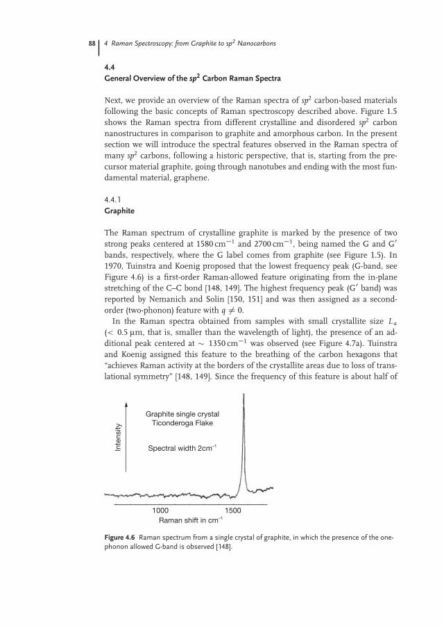
4.4.1Graphite
The Raman spectrum of crystalline graphite is marked by the presence of twostrong peaks centered at 1580 cm�1 and 2700 cm�1, being named the G and G0
bands, respectively, where the G label comes from graphite (see Figure 1.5). In1970, Tuinstra and Koenig proposed that the lowest frequency peak (G-band, seeFigure 4.6) is a first-order Raman-allowed feature originating from the in-planestretching of the C–C bond [148, 149]. The highest frequency peak (G0 band) wasreported by Nemanich and Solin [150, 151] and was then assigned as a second-order (two-phonon) feature with q ¤ 0.
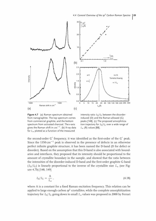
In the Raman spectra obtained from samples with small crystallite size L a
(< 0.5 µm, that is, smaller than the wavelength of light), the presence of an ad-ditional peak centered at � 1350 cm�1 was observed (see Figure 4.7a). Tuinstraand Koenig assigned this feature to the breathing of the carbon hexagons that“achieves Raman activity at the borders of the crystallite areas due to loss of trans-lational symmetry” [148, 149]. Since the frequency of this feature is about half of
Inte
nsity
Graphite single crystalTiconderoga Flake
Spectral width 2cm–1
1000 1500Raman shift in cm–1
Figure 4.6 Raman spectrum from a single crystal of graphite, in which the presence of the one-phonon allowed G-band is observed [148].
4.4 General Overview of the sp2 Carbon Raman Spectra 89
1500 00.0
0.5
1.0
1.5
2.0 a·C nc·G
Tuinstra Koenig
α La
2.5
1.0
I1355
I1575
0.1
10
20
30103
La(A)
5 10
I(D)/
I(G)
15 20 20
°
°La(A)60 100 140 180 220 3002601000
Inte
nsity
Raman shift in cm–1
2
α 1/La
(a) (c)
(b)
Figure 4.7 (a) Raman spectrum obtainedfrom nanographite. The top spectrum comesfrom commercial graphite, and the bottomspectrum from activated charcoal. The x-axisgives the Raman shift in cm�1. (b) X-ray datafor La plotted as a function of the measured
intensity ratio ID/IG between the disorder-induced (D) and the Raman-allowed (G)peaks [148]. (c) The proposed amorphitiza-tion trajectory for ID/IG over a wide range ofLa (Å) values [88].
the second-order G0 frequency, it was identified as the first-order of the G0 peak.Since the 1350 cm�1 peak is observed in the presence of defects in an otherwiseperfect infinite graphite structure, it has been named the D-band (D for defect ordisorder). Based on the assumption that this D-band is also associated with bound-aries and interfaces, they proposed that its intensity should be proportional to theamount of crystallite boundary in the sample, and showed that the ratio betweenthe intensities of the disorder-induced D-band and the first-order graphite G-band(ID/IG) is linearly proportional to the inverse of the crystallite size L a (see Fig-ure 4.7b) [148, 149]
ID/IG D AL a
, (4.18)
where A is a constant for a fixed Raman excitation frequency. This relation can beapplied to large enough carbon sp2 crystallites, while the complete amorphitizationtrajectory for ID/IG going down to small L a values was proposed in 2000 by Ferrari
90 4 Raman Spectroscopy: from Graphite to sp2 Nanocarbons
and Robertson [88] (see Figure 4.7c). As proposed by Ferrari and Robertson, ID/IG
starts to decrease for sp2 carbon hexagonal structure starts to disappear. Further-more, this ID/IG intensity ratio was further shown to be excitation laser energy-dependent [152]. Another disorder-induced band centered at 1620 cm�1 is usuallyobserved in the Raman spectra of disordered graphitic materials, although withsmaller intensity as compared to the D-band. This feature, reported in 1978 by Tsuet al. [153], has been named the D0-band and also depends on L a and Elaser [153].
In 1981, Vidano et al. [154] showed that the D and G0-band are dispersive,that is, their frequencies change with the incident laser energy Elaser [154] with∆ωD/∆Elaser � 50 cm�1/eV and ∆ωG0 /∆Elaser � 100 cm�1/eV. The out-of-planestacking order has also been shown to affect the G0 Raman spectra [155–157].Baranov et al. [158] proposed, in 1987, that the dispersive behavior of the D-bandcomes from the coupled resonance between the excited electron and the scatteredphonons, as previously discussed in semiconductor physics [91, 142]. The fullappreciation of the double resonance model came in 2000, as discussed by Thom-sen and Reich [159], and extended to explain the mechanism behind many otherdispersive Raman peaks usually observed in the literature [160], yielding an expla-nation for all the features observed in the Raman spectra of ordered and disorderedgraphite [88]. Many of the weak Raman features are dispersive and can be used tomeasure the graphite phonon dispersion [160], that is, the atomic vibrations withdifferent wave vectors, usually obtained only with inelastic neutron scattering dueto momentum conservation requirements. Another interesting result obtained bythe double resonance model (see Chapter 13) was the definition of the atomicstructure at graphite edges [161].
In parallel to the solid state physics approach for exhibiting the Raman spectraof sp2 carbons, a molecular approach to the Raman spectroscopy of graphite hasdeveloped based on polycyclic aromatic hydrocarbons (PAH) [162–164]. Here PAHdenotes a class of planar two-dimensional π-conjugated structures consisting ofcondensed aromatic rings, with a structure similar to graphene (see Figure 4.8).The PAHs can be synthesized with well-defined size and shape [165, 166], allow-ing study of the effects of the confinement and de-localization of π-electrons usingquantum chemistry calculations. The quantum chemical studies show two collec-tive vibrational displacements characteristic of PAHs giving rise to strong Ramansignals, the first appearing in the frequency range 1200–1400 cm�1, with a largeprojection of a totally symmetric atomic vibration related to the D-band, and thesecond appearing in the frequency range 1600–1700 cm�1, with a large projectionon the G-band displacement (see Figure 4.8). The D-like band is active in PAHsdue to the relaxation of the structure correlated with the confinement of π elec-trons. The confinement and de-localization effects can be induced in the presenceof finite-size graphite domains or edges. These effects change progressively withthe molecular size in connection with disordered and nanostructured sp2 carbonmaterials, and exhibit a clear size-dependent resonance phenomenon. These con-cepts have been behind the development of long-range electron–phonon couplingmodels for the periodic graphene structure, such as for the Kohn anomaly, dis-cussed in Chapter 8 [141].
4.4 General Overview of the sp2 Carbon Raman Spectra 91
Figure 4.8 (a) nuclear displacements asso-ciated with the G-band (at Γ point) and D-band phonons (at the K point) of a perfect 2Dgraphene monolayer. (b) comparison with se-
lected normal modes of C114H30, as obtainedfrom semi-empirical quantum consistent-force-field π electron method (QC FF/PI) cal-culations [167].
At this point, the main ingredients responsible for the large impact of Ramanspectroscopy on sp2 nanocarbons are already in place. The G-band gives the first-order signature. As we will see, the G-band exhibits a rich behavior for nanostruc-tured systems due to quantum confinement effects, curvature effects and electron–phonon coupling. The G0-band is sensitive to small changes in both the electronicand vibrational structures, and acts as a probe for electrons and phonons and theiruniqueness in each distinct sp2 nanocarbon. The disorder-induced D-band (and al-so the smaller intensity D0-band) appears due to symmetry-breaking effects, and,together with theory, can provide valuable information about local disorder. TheD-band is a second-order process that includes an inelastic scattering event andthus D-band is not the first-order process of the G0-band which only involves twophonon scattering processes of the same phonon as for the D-band. Finally, manyother small features can be observed and related to specific physical properties.
To conclude this brief review of the Raman spectra of graphite, we note that whenstrong amorphitization takes place, substantially increasing the sp3 carbon sam-ple content, significant changes in the Raman lineshapes are observed [88]. Amor-phous carbon and diamond-like materials have been intensively studied and thesematerials have been broadly utilized in surface coating applications. This book willdiscuss in depth the disorder-induced features related to symmetry breaking of thesp2 configuration, but discussion of the Raman spectra associated with amorphi-tization is beyond the scope of this volume. For more discussion on sp3 carbonsystems, see for example [88].
92 4 Raman Spectroscopy: from Graphite to sp2 Nanocarbons
4.4.2Carbon Nanotubes – Historical Background
The use of Raman spectroscopy to characterize carbon materials generally [90, 168]motivated researchers to apply this technique also to SWNTs shortly after the earlysynthesis of SWNTs in 1993 [25, 26]. Even though only � 1% of the carbonaceousmaterial in the sample used in the 1994 experiments was estimated to be due toSWNTs [169], a unique Raman spectrum was observed, different from any oth-er previously observed spectrum, namely a double-peak G-band structure. Thesefindings motivated further development of this noninvasive characterization tech-nique for SWNTs, and the laser ablation technique, developed in 1996 to synthesizelarge enough quantities of high purity SWNT material [170], opened up this fieldof investigation [136].
The first phase explorations of Raman spectroscopy on SWNTs spanned the fouryear period 1997–2001. Figure 4.9 gives a general view of the Raman spectra from atypical SWNT bundle sample. There are two dominant Raman signatures in theseRaman spectra that distinguish a SWNT from other forms of carbon. The firstrelates to the low frequency feature, usually in the range 100–300 cm�1, arisingfrom phonon scattering by the radial breathing mode (RBM), which correspondsto symmetric in-phase displacements of all the carbon atoms in the radial direction
500 1000 1500
RBM
G band
2000
1700
1500
1300
A LO
TO
Γ Κq
ω (κ
) (cm
–1) E2E1
Wavenumbers
Wavenumbers1450 1500 1550 1600 1650
Ram
an in
tens
ity
Ram
an in
tens
ity
(a) (d)
(b) (c)
Figure 4.9 (a) Room temperature Ramanspectrum from a SWNT bundle grown by thelaser vaporization method. The inset showsa Lorentzian fit to the G-band multiple fea-ture [112, 136]. (b) The G-band eigenvectorsfor the C–C bond stretching mode. The G-band is composed of up to six peaks that areallowed in the first-order Raman spectra. Thevibrations are tangential to the tube surface,three along the tube axis (LO) and three along
the circumference (TO), having two modeswith A, E1 and E2 symmetries. Within the setof three peaks, what changes is the relativephase of the vibration, containing 0, 2 or 4nodes along the tube circumference, whichis related to increasing q in the unfoldedgraphene phonon dispersion ω(q) along Γ Kin the Brillouin zone (c). (d) Eigenvector forthe radial breathing mode (RBM) appearingaround 186 cm�1 in (a).
4.4 General Overview of the sp2 Carbon Raman Spectra 93
(see Figure 4.9d). The second signature relates to the multi-component higher fre-quency features (around 1500–1600 cm�1) associated with the tangential (G-band)vibrational modes of SWNTs and is related to both the early observations in [169]and to the Raman-allowed feature appearing in Raman spectra for graphite (seeFigure 4.9b,c). Neither the RBM feature nor the multi-component G-band featuresin the Raman spectra for SWNTs were previously observed in any other sp2 bondedcarbon material.
Like in graphite, several studies were carried out on the D, G, G0 bands of carbonnanotubes, as well as on other combination modes and overtones [112]. The powerof Raman spectroscopy for studying carbon nanotubes was in particular revealedthrough exploitation of the resonance Raman effect, which is greatly enhanced bythe singular density of electronic states, which comes from one-dimensional con-finement of the electronic states. Soon after the discovery of the resonance Ramaneffect in SWNTs [136], it was found that the resonance lineshape could be used todistinguish metallic from semiconducting SWNTs. Specifically, the lineshape forthe lower frequency G-band feature (G�) is broader for a metallic tube, and this fea-ture follows a Breit–Wigner–Fano lineshape, and downshifted in frequency fromthat for a semiconducting tube of similar diameter (see Figure 4.10a) [147, 171].The RBMs from SWNT bundles were found to exhibit an oscillatory behavior de-pending on the excitation laser energy, due to the confinement of the electronicstructure [172], and a similar effect was observed for the G0 band [173]. The in-terpretation of all these resonance Raman effects was systematized by the develop-
1400 1500 1600 1700
Ram
an in
tens
ity
Raman shift (cm 1)
0.941.171.59
1.831.922.072.102.142.412.713.05
1.70
(eV)
laser
1.00 1.25 1.50 1.75
1.0
1.5
2.0
2.5
3.0
Nanotube diameter (nm)
Tran
sitio
n en
ergy
Eii (
eV)
(a) (b)
Figure 4.10 (a) Raman spectra of the tan-gential G-band modes of carbon nanotubebundles measured with several different laserlines showing lineshapes typical of semicon-ducting and metallic carbon nanotubes, takenfrom [171]. (b) Optical transition energiesfor the nanotube diameter distribution in thebundles (the vertical solid line is the averagenanotube diameter and the vertical dashed
lines define the full width at half maximum di-ameter distribution of the nanotube sample).Crosses denote optical transition energiesfor semiconducting nanotubes and open cir-cles are for metallic SWNTs. The G-band getsbroad and downshifted when the laser is inresonance with optical transitions from metal-lic SWNTs, as shown in (a) [110].
94 4 Raman Spectroscopy: from Graphite to sp2 Nanocarbons
ment, in 1999, of the so-called Kataura plot, where Kataura and coworkers displayedthe optical transition energies for each (n, m) SWNT as a function of tube diame-ter [174], as shown in Figure 4.10b. Advances in the synthesis of carbon nanotubesalso took place in the 1997–2001 time frame, allowing the use of catalyzed chemicalvapor deposition (CVD) techniques in the growth of samples of isolated individualSWNTs on an insulating substrate, such as oxidized silicon (Si/SiO2) [175].
The second phase explorations of the Raman spectroscopy of SWNTs spannedthe four year period 2001–2004 and this phase was opened by the observation ofRaman spectra from a single isolated SWNT [176], as shown in Figure 4.11. Mea-surements of the frequency of the radial breathing mode and the resonant energyEi i at the single nanotube level allow a determination to be made of the (n, m) in-
Figure 4.11 (a) Raman spectra from SWNTsat the single nanotube level. The Raman fea-tures denoted by “*” come from the Si/SiO2substrate on which the nanotube is mount-
ed. (b) Atomic force microscopy image of theSWNT sample used in the experiment. Theinset (lower right) shows the diameter distri-bution of the sample in (b) [176].
Figure 4.12 (a) The G-band for highly orientedpyrolytic graphite (HOPG), one semicon-ducting SWNT and one metallic SWNT. ForC60 fullerenes a peak in the Raman spectra isobserved at 1469 cm�1, but it is not consid-ered a G-band. (b) The radial breathing mode
(RBM) and the G-band Raman spectra forthree semiconducting isolated SWNTs withthe indicated (n, m) values. (c) Frequency vs.1/dt for the two most intense G-band features(ωG� and ωGC ) from isolated semiconduct-ing and metallic SWNTs [179].
4.4 General Overview of the sp2 Carbon Raman Spectra 95
tegers of a SWNT as a function of nanotube diameter dt and chiral angle θ [31].Once the (n, m) of a given tube is identified, then the dependence of the frequen-cy, width and intensity of each of the features in the Raman spectra on diameterand chiral angle can be found, including the RBM, G-band, D-band, G0-band, andvarious overtone and combination modes within the first-order and higher-orderfrequency regimes (see Figure 4.12 for the ωG dependence on 1/dt) [80, 179]. Suchstudies have played a major role in advancing both the fundamental understand-ing of Raman spectroscopy for 1D systems and in characterizing actual SWNTsamples [80, 177, 178].
Third phase explorations of Raman spectroscopy on SWNTs started in 2004. Itwas initiated by both the development of the high pressure CO (HiPCO) and com-pact synthesis processes for nanotubes, that generated a large amount of SWNTs inthe low diameter limit of 0.7–1.3 nm, and the development of a method for dispers-ing the nanotube bundles to produce isolated tubes in solution. The presence ofisolated tubes with relatively small diameters allowed detailed studies to be madeof the first electronic transition E S
11 for semiconducting nanotubes using mostlyphotoluminescence experiments [180] (Ei i / 1/dt, E S
11 being in the far-infraredspectral range for usual tube diameters dt > 1.3 nm). Studies on the small diam-eter SWNTs led to an observation of the departure from the tight-binding modelwhich predicted the “ratio rule”, that is, E S
22/E S11 D 2 for armchair tubes [181]. The
observation of 2n C m family effects [180, 182] led to much more sophisticated firstprinciples and tight-binding models for treating many-body effects in 1D systems.
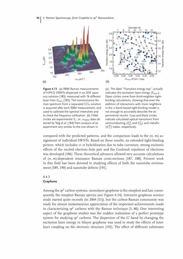
In order to accurately study the optical transition energies, resonance Raman ex-periments with many laser lines and tunable laser systems (based on dye lasersand Ti:Sapphire laser systems) started to be made [183, 184]. Using several close-ly spaced excitation laser energies, 2D plots were made from the RBM spectraobtained from Stokes resonance Raman measurements as a function of Elaser.Figure 4.13a presents a map of Stokes resonance Raman measurements of car-bon nanotubes grown by the HiPCO process, dispersed in aqueous solution andwrapped with sodium dodecyl sulfate (SDS) [185], in the frequency region of theRBM features, built from 76 values of Elaser for 1.52 Elaser 2.71 eV. SeveralRBM peaks appear in Figure 4.13a, each peak corresponding to an (n, m) SWNTin resonance with Elaser, thereby delineating for each nanotube both the resonancespectra as a function of Elaser and the resonance window (Raman intensity as afunction of the energy in the range where the RBM feature can be observed).
Figure 4.13b shows a comparison between the experimental and theoreticalKataura plots. The filled circles are experimental Ei i vs. ωRBM obtained by Telget al. [184] from analysis of an experiment very similar to the one performed byFantini et al. [183] and shown in Figure 4.13a. The open circles come from a third-neighbor tight-binding calculation [184]. Black and gray open circles represent, re-spectively, M-SWNTs and S-SWNTs. The geometrical patterns for carbon nanotubefamilies with (2n C m) D constant (dashed gray lines) for E S
22, E M11 and E S
33 arealso shown along with the (n, m) values assigned for some SWNTs. The energiesdo not match very well due to the simplicity of the TB method, even going up tothird-neighbor interactions. However, the observed geometrical patterns can be
96 4 Raman Spectroscopy: from Graphite to sp2 Nanocarbons
Figure 4.13 (a) RBM Raman measurementsof HiPCO SWNTs dispersed in an SDS aque-ous solution [185], measured with 76 differentlaser lines Elaser [183]. The nonresonance Ra-man spectrum from a separated CCl4 solutionis acquired after each RBM measurement, andused to calibrate the spectral intensities andto check the frequency calibration. (b) Filledcircles are experimental Ei i vs. ωRBM data ob-tained by Telg et al. [184] from analysis of anexperiment very similar to the one shown in
(a). The label “Transition energy exp.” actuallyindicates the excitation laser energy (Elaser).Open circles come from third-neighbor tight-binding calculations, showing that even theaddition of interactions with more neighborsin the π-band based tight-binding model isnot enough to accurately describe the ex-perimental results. Gray and black circlesindicate calculated optical transitions fromsemiconducting (E S
22 and E S33) and metallic
(E M11 ) tubes, respectively.
compared with the predicted patterns, and the comparison leads to the (n, m) as-signment of individual SWNTs. Based on these results, an extended tight-bindingpicture, which includes σ–π hybridization due to tube curvature, strong excitoniceffects of the excited electron–hole pair and the Coulomb repulsion of electronswas developed [186]. These theoretical advances allowed very accurate calculationsof (n, m)-dependent resonance Raman cross-sections [187, 188]. Present workin this field has been devoted to studying effects of both the nanotube environ-ment [189, 190] and nanotube defects [191].
4.4.3Graphene
Among the sp2 carbon systems, monolayer graphene is the simplest and has, conse-quently, the simplest Raman spectra (see Figure 4.14). Intensive graphene sciencestudy started quite recently (in 2004 [51]), but the carbon-Raman community wasready for almost instantaneous appreciation of the important achievements madein characterizing sp2 carbons with the Raman technique [5, 86]. One interestingaspect of the graphene studies was the sudden realization of a perfect prototypesystem for studying sp2 carbons. The dispersion of the G0-band by changing theexcitation laser energy in bilayer graphene was used to study the effects of inter-layer coupling on the electronic structure [192]. The effect of different substrates
4.4 General Overview of the sp2 Carbon Raman Spectra 97
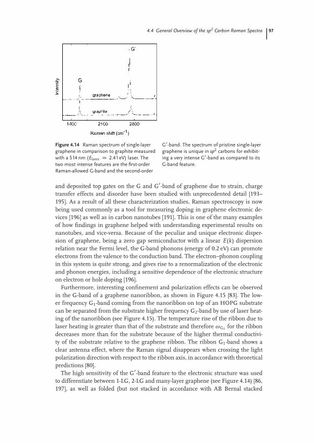
Figure 4.14 Raman spectrum of single-layergraphene in comparison to graphite measuredwith a 514 nm (Elaser D 2.41 eV) laser. Thetwo most intense features are the first-orderRaman-allowed G-band and the second-order
G0-band. The spectrum of pristine single-layergraphene is unique in sp2 carbons for exhibit-ing a very intense G0-band as compared to itsG-band feature.
and deposited top gates on the G and G0-band of graphene due to strain, chargetransfer effects and disorder have been studied with unprecedented detail [193–195]. As a result of all these characterization studies, Raman spectroscopy is nowbeing used commonly as a tool for measuring doping in graphene electronic de-vices [196] as well as in carbon nanotubes [191]. This is one of the many examplesof how findings in graphene helped with understanding experimental results onnanotubes, and vice-versa. Because of the peculiar and unique electronic disper-sion of graphene, being a zero gap semiconductor with a linear E(k) dispersionrelation near the Fermi level, the G-band phonons (energy of 0.2 eV) can promoteelectrons from the valence to the conduction band. The electron–phonon couplingin this system is quite strong, and gives rise to a renormalization of the electronicand phonon energies, including a sensitive dependence of the electronic structureon electron or hole doping [196].
Furthermore, interesting confinement and polarization effects can be observedin the G-band of a graphene nanoribbon, as shown in Figure 4.15 [83]. The low-er frequency G1-band coming from the nanoribbon on top of an HOPG substratecan be separated from the substrate higher frequency G2-band by use of laser heat-ing of the nanoribbon (see Figure 4.15). The temperature rise of the ribbon due tolaser heating is greater than that of the substrate and therefore ωG1 for the ribbondecreases more than for the substrate because of the higher thermal conductivi-ty of the substrate relative to the graphene ribbon. The ribbon G1-band shows aclear antenna effect, where the Raman signal disappears when crossing the lightpolarization direction with respect to the ribbon axis, in accordance with theoreticalpredictions [80].
The high sensitivity of the G0-band feature to the electronic structure was usedto differentiate between 1-LG, 2-LG and many-layer graphene (see Figure 4.14) [86,197], as well as folded (but not stacked in accordance with AB Bernal stacked
98 4 Raman Spectroscopy: from Graphite to sp2 Nanocarbons
Figure 4.15 (a) The G-band Raman spectrafrom a graphene nanoribbon (G1) and fromthe graphite substrate on which the nanorib-bon sits (G2). (b) The G1 peak intensity de-pendence on the light polarization directionwith respect to the ribbon axis, including
experimental points on the dark curve andtheoretical predictions by the dashed curve.(c) Frequency of the G-band peaks as a func-tion of incident laser power for the grapheneribbon (G2) in contrast to the results for theHOPG substrate (G1) [83].
graphite) layers [198]. The Raman technique soon became the fingerprint for quickcharacterization of few-layer graphene samples. Raman imaging also differentiatesbetween the number of layers in different locations of a large graphene flake, dueto the dependence of the Raman intensity on the number of scattering layers [197],although this information has not yet provided an accurate characterization toolfor determining the number of layers in few-layer graphene. The epitaxial growthof graphene on a SiC substrate, among others, and the effect of other chemical-ly induced environmental interactions has also been studied using Raman spec-troscopy [199].
Problems
[4-1] This problem tests your understanding of the difference between resonanceRaman scattering (RRS) and hot luminescence (PL) processes. Consider amaterial with a discrete optical level with energy Eg and a phonon withenergy Eq. Build a plot of Ei vs. Es and show how the PL and the RRSshould appear in such a plot. Make schematic pictures to show you candifferentiate the two processes when they overlap in energy.
4.4 General Overview of the sp2 Carbon Raman Spectra 99
[4-2] Obtain Eq. (4.7) from Eq. (4.6).
[4-3] Consider the equation for a damped harmonic oscillator driven by a forceF0
m@2x
@t2 C γ@x
@tC K x D F0 exp i(ω t C φ) . (4.19)
a. Obtain and plot the oscillator response x as a function of the drivingfrequency ω.
b. Show that the power response (jx j2) exhibits a Lorentzian lineshapewhen the natural oscillator frequency is much larger than the peak fullwidth at half maximum intensity. Obtain an expression for the time de-pendence of the full width at half maximum intensity.
[4-4] Show that 1 eV corresponds to 8065 cm�1. What is the energy in eV for theG-band Raman spectrum of graphite at 1580 cm�1?
[4-5] Obtain the energy in eV of a laser with a wavelength of 633 nm. What is theconversion formula from nm to eV, and from eV to nm?
[4-6] What is the wavelength of the Stokes and anti-Stokes scattered light for thegraphene (1590 cm�1) G-band for 514.5 nm laser light?
[4-7] When we consider the room temperature Raman spectrum for a carbonnanotube at 300 K, what is the intensity ratio of the anti-Stokes and Stokesintensities IaS/IS for the G-band (1590 cm�1) and for the radial breathingmode for a 1nm diameter SWNT, with ωRBM D 227 cm�1? When the tem-perature is changed to 4 K and to 2000 K, what are the new values of IaS/IS
for these cases?
[4-8] Derive the relation between the Raman peak FWHM and phonon lifetime.
[4-9] Calculate the wave vectors for 488 nm, 514 nm, 633 nm lasers and comparethem with the wave vector of the K and M points of graphene.
[4-10] Consider the linear dispersion of energy for graphene,
E(k) D ˙p
3γ0
2
�qk2
x C k2y
�a ,
where ˙ denote the valence and conduction bands, respectively, and γ0 D2.9 eV (nearest neighbor transfer energy for an optical transition) and a D0.246 nm. Show that this energy dispersion has the shape of two cone struc-tures with the apexes of their Dirac cones that touch each other at the K(Dirac) point. Calculate the jkj value (distance from the Γ point in k space)for an optical transition observed with a 514 nm laser.
[4-11] In Problem 4-10, when an optical phonon (LO branch) with energy1580 cm�1 is emitted, show the energy-momentum conserved final states
100 4 Raman Spectroscopy: from Graphite to sp2 Nanocarbons
in the energy dispersion and show the possible q vectors in a figure. (Hint:the final states should be on an equi-energy contour of Elaser � Eq).
[4-12] In the case of graphene, the Dirac cone shape appears not only at the K pointbut also at the K 0 point. Explain in what ways K and K 0 are not equivalentto each other. If we consider the inelastic scattering from k in the K Diraccone to k � q in the K 0 Dirac cone, plot the possible q vectors measuredfrom the Γ point in the two-dimensional Brillouin zone.
[4-13] In the previous problem, for a given laser excitation, the k wave vector forphotoexcited electrons exists on an equi-energy contour. Plot the possible qvectors in the two-dimensional Brillouin zone.
[4-14] The condition for the resonance Raman effect is given by Elaser D Egap,where Egap denotes the energy separation between the conduction and va-lence energy bands. If the resonance condition is applied for the scatteredresonance for phonon energy Eq, show the resonance condition for the scat-tered light, which we call the scattered light resonance condition. Explainwhy the scattered light resonance condition depends on the phonon energywhile the incident light resonance condition does not.
[4-15] When we plot the Raman intensity as a function of Elaser (Raman excitationprofile), we expect two peaks: one for the incident resonance and one for thescattered resonance conditions. When we have two different phonons withdifferent phonon energies, illustrate the expected Raman excitation profiles.
[4-16] Explain the resonance conditions for anti-Stokes shifts. Illustrate two Ra-man excitation profiles for the Stokes and anti-Stokes Raman signals. Ex-plain why the two Raman excitation profiles do not appear at the same exci-tation energy values.
[4-17] If we consider second-order Raman scattering for a q ¤ 0 phonon forgraphene, we have two distinct q vectors for a q ¤ 0 scattering event. Ex-plain this situation by using the two Dirac cone model. We denote these twoscattering events by intravalley scattering and intervalley scattering.
[4-18] Explain the results in Problem 4-17 with an illustration of intervalley scat-tering for the forward (q) and backward (�q) scattering geometries.
[4-19] Explain in the phonon dispersion of graphene (Figure 3.1), which phononsare selected for intravalley and intervalley q ¤ 0 scattering. Explain whathappens for the case of forward and backward scattering.
[4-20] For an intravalley process, when we consider two laser energies E1 < E2,show that the q vectors are larger for Elaser D E2. When the laser energyincreases, how is the scattered q vector selected in the phonon energy dis-persion?
[4-21] If Elaser is selected in the Raman measurement of single-wall carbon nan-otubes (SWNTs), we can get a Raman signal only from SWNTs, which satis-
4.4 General Overview of the sp2 Carbon Raman Spectra 101
fy the resonance condition Elaser D Ei i . When we observe the radial breath-ing mode (RBM) whose frequency is inversely proportional to the diameter,how can we determine (n, m) values from the known calculated values ofEi i and ωRBM? Explain a procedure that could be used to get (n, m) values.
[4-22] In order to obtain all the (n, m) values for SWNTs in a given sample, weneed an almost continuously tunable energy output from Elaser. Supposethat you have a laser system with continuously tunable energy, how shouldyou arrange the experimental schedule to obtain all these (n, m) values?Explain your purpose and the method you will use.
[4-23] Suppose that we have only one SWNT on a Si substrate. The position ofthe SWNT cannot be seen by optical microscopy. Explain why obtaining(n, m) for the specified SWNT by Raman spectroscopy is difficult. In orderto overcome this difficulty, how should we prepare our samples or arrangeour experimental set up?
[4-24] Try to correlate the modifications in the G0 feature, as shown in Figure 4.14bwith the changes in the electronic structure, as discussed in Section 2.2.4.
[4-25] How should the ID/IG intensity ratio depend on the defect density in agraphene layer? Discuss a physical picture for some defect density conditionwith use of some typical lengths of the system.