33
Design of a Transceiver for 3G DECT Physical Layer - Rohit Budhiraja

Design of a Transceiver for 3G DECT Physical Layer
- Rohit Budhiraja
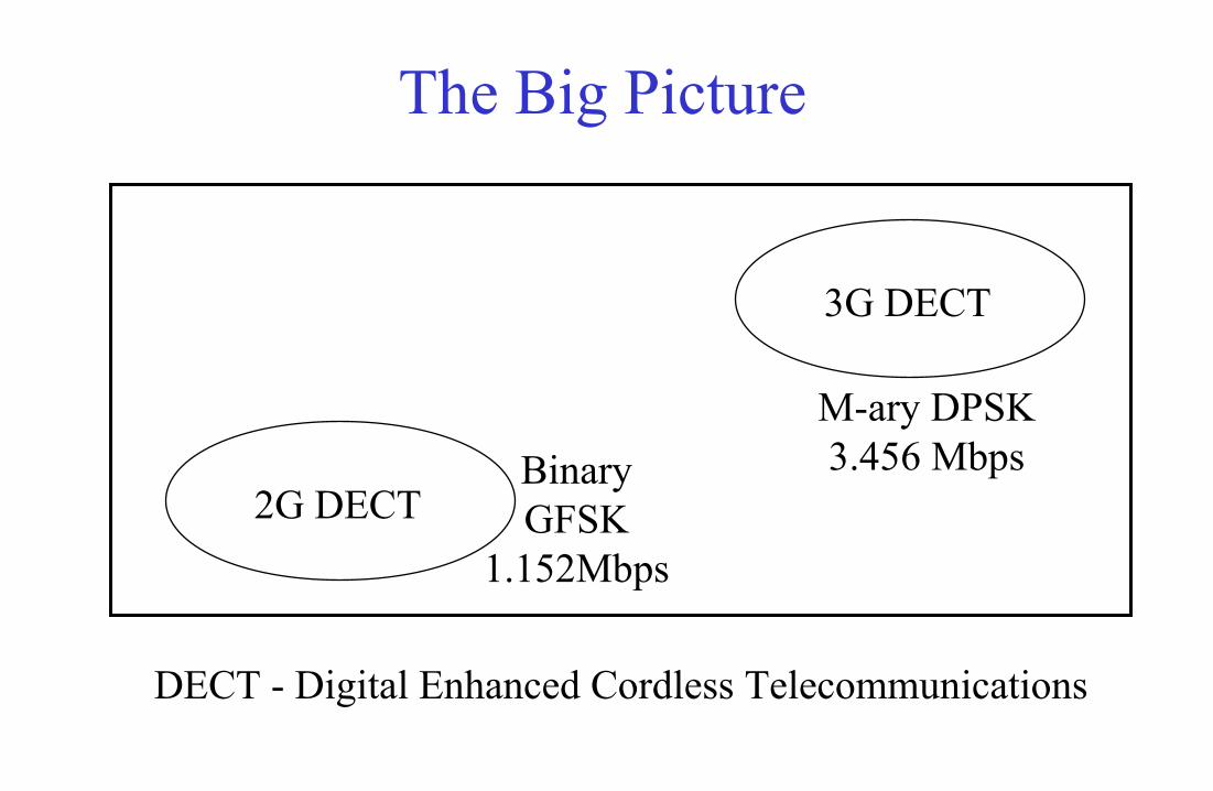
The Big Picture
DECT - Digital Enhanced Cordless Telecommunications
2G DECT
3G DECT
BinaryGFSK
1.152Mbps
M-ary DPSK3.456 Mbps

• 2G DECT specifications and 2G transceiver
• 3G DECT specifications
• Issues in receiver design
• Digital FM demodulator
• Coherent detector for DPSK symbols
• Results and Conclusion
Overview
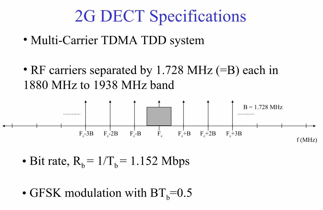
• Multi-Carrier TDMA TDD system
• RF carriers separated by 1.728 MHz (=B) each in 1880 MHz to 1938 MHz band
2G DECT Specifications
• Bit rate, Rb = 1/Tb = 1.152 Mbps
• GFSK modulation with BTb=0.5
f (MHz)Fc+BFc-BFc-2BFc-3B Fc Fc+2B Fc+3B
B = 1.728 MHz
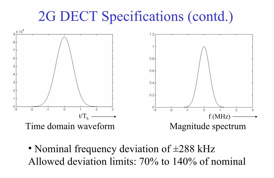
2G DECT Specifications (contd.)
Time domain waveform Magnitude spectrumf (MHz)t/Tb
• Nominal frequency deviation of ±288 kHz Allowed deviation limits: 70% to 140% of nominal
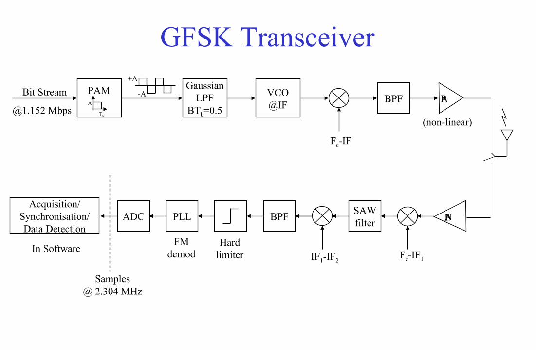
GFSK Transceiver
Fc-IF1
SAWfilter
IF1-IF2
PLL
Hardlimiter
ADC BPF LNAAcquisition/
Synchronisation/Data Detection
FMdemodIn Software
Samples@ 2.304 MHz
+A
-ABit Stream PAMA
Tb
GaussianLPF
BTb=0.5
VCO@IF
Fc-IF
PABPF
(non-linear)@1.152 Mbps
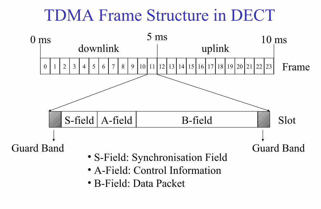
TDMA Frame Structure in DECT
0 1 2 3 4 5 6 7 8 9 10 11 12 13 14 15 16 17 18 19 20 21 22 23
downlink uplink0 ms 5 ms 10 ms
Frame
Slot
• S-Field: Synchronisation Field• A-Field: Control Information• B-Field: Data Packet
S-field A-field B-field
Guard BandGuard Band
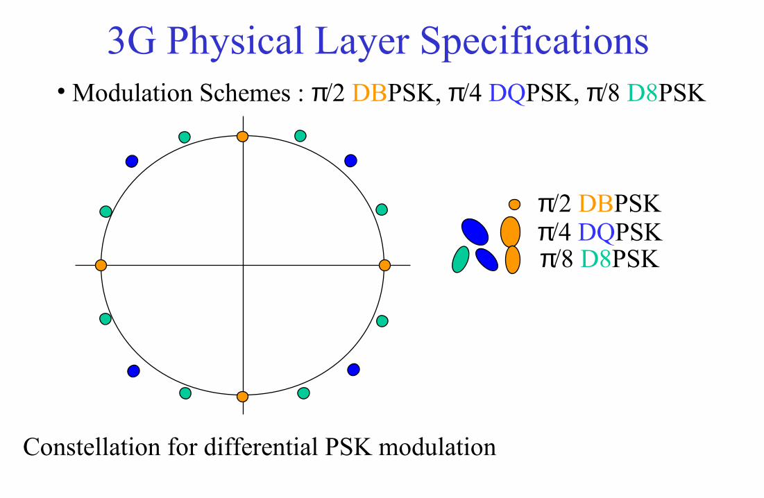
• Modulation Schemes : π/2 DBPSK, π/4 DQPSK, π/8 D8PSK
π/2 DBPSKπ/4 DQPSK
Constellation for differential PSK modulation
π/8 D8PSK
3G Physical Layer Specifications
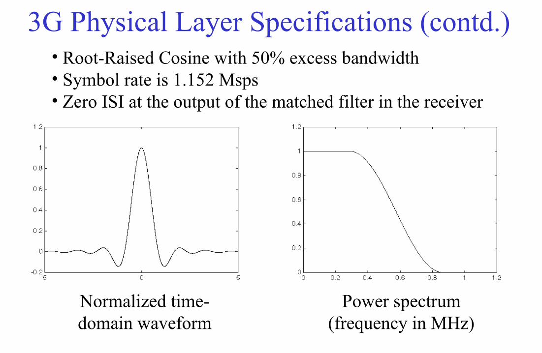
Normalized time-domain waveform
Power spectrum(frequency in MHz)
• Root-Raised Cosine with 50% excess bandwidth• Symbol rate is 1.152 Msps• Zero ISI at the output of the matched filter in the receiver
3G Physical Layer Specifications (contd.)
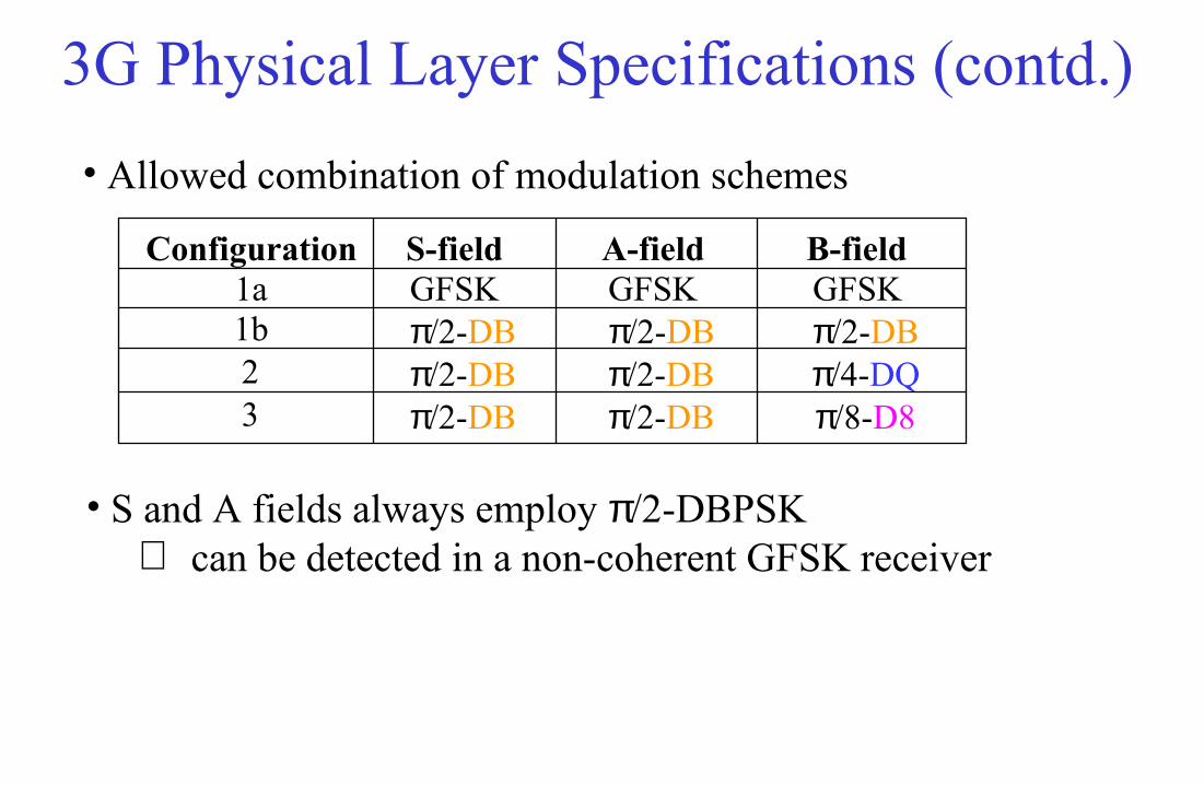
3G Physical Layer Specifications (contd.)
• Allowed combination of modulation schemes
• S and A fields always employ π/2-DBPSK ⇒ can be detected in a non-coherent GFSK receiver
Configuration S-field A-field B-field1a GFSK GFSK GFSK1b π/2-DB π/2-DB π/2-DB2 π/2-DB π/2-DB π/4-DQ3 π/2-DB π/2-DB π/8-D8
Signal processingin digital domain
IF1+IF2
ADCBit Stream
BPF2
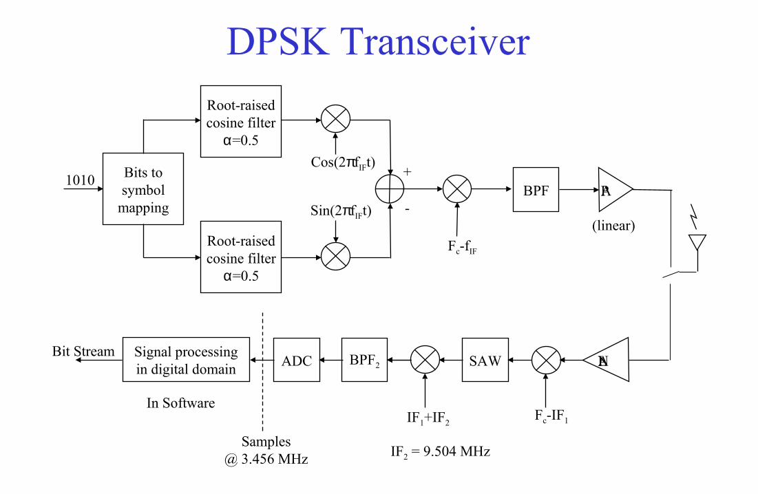
Root-raisedcosine filter
α=0.5
1010 Bits tosymbol
mapping
Root-raisedcosine filter
α=0.5
Cos(2πfIFt)
Sin(2πfIFt)
+
-
Fc-fIF
Fc-IF1
SAW LNA
PABPF
(linear)
DPSK Transceiver
In Software
Samples@ 3.456 MHz IF2 = 9.504 MHz
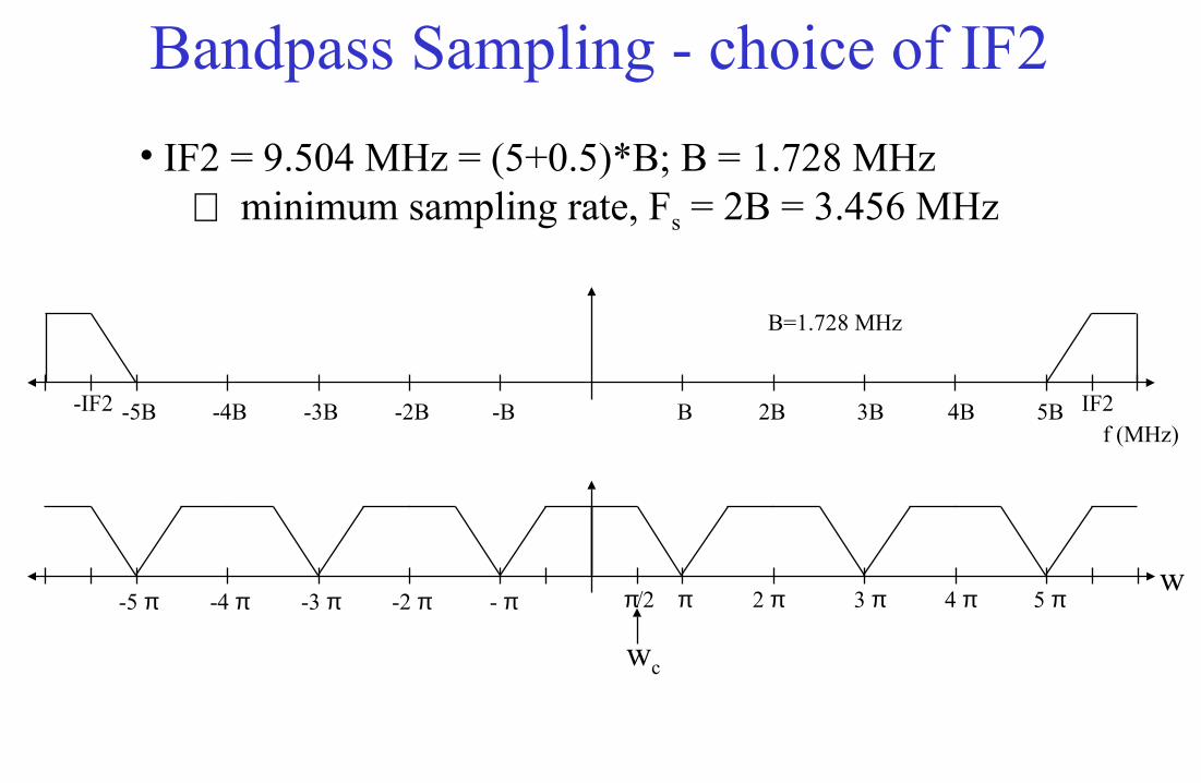
Bandpass Sampling - choice of IF2
• IF2 = 9.504 MHz = (5+0.5)*B; B = 1.728 MHz⇒ minimum sampling rate, Fs = 2B = 3.456 MHz
f (MHz)IF2-IF2 B 2B 3B 4B 5B-B-2B-3B-4B-5B
B=1.728 MHz
wπ 2 π 3 π 4 π 5 π- π-2 π-3 π-4 π-5 π π/2
wc
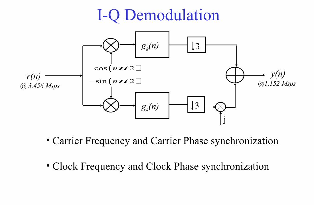
I-Q Demodulation
• Carrier Frequency and Carrier Phase synchronization
• Clock Frequency and Clock Phase synchronization
r(n)
gk(n)
( )cos / 2nπ
( )sin / 2nπ−
gk(n)
y(n)@ 3.456 Msps @1.152 Msps
3
3
j
θ
I
Q
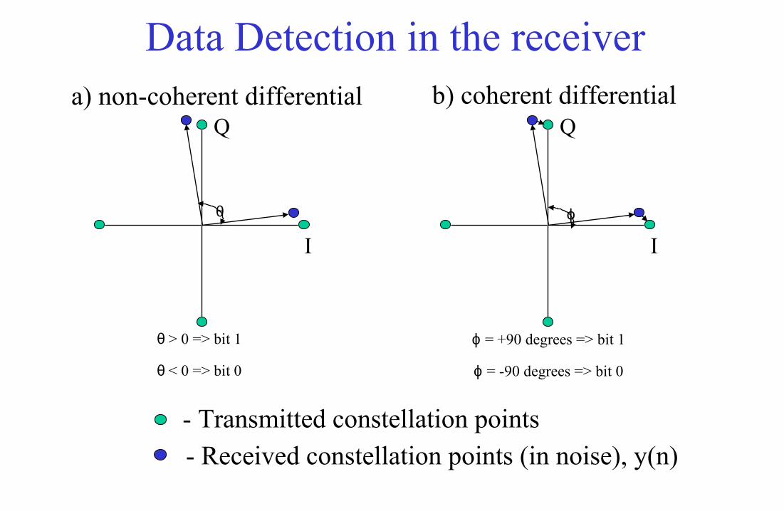
- Transmitted constellation points
- Received constellation points (in noise), y(n)
θ > 0 => bit 1
θ < 0 => bit 0
I
Q
ϕ = +90 degrees => bit 1
ϕ = -90 degrees => bit 0
ϕ
Data Detection in the receivera) non-coherent differential b) coherent differential

Performance of Different DemodulationSchemes
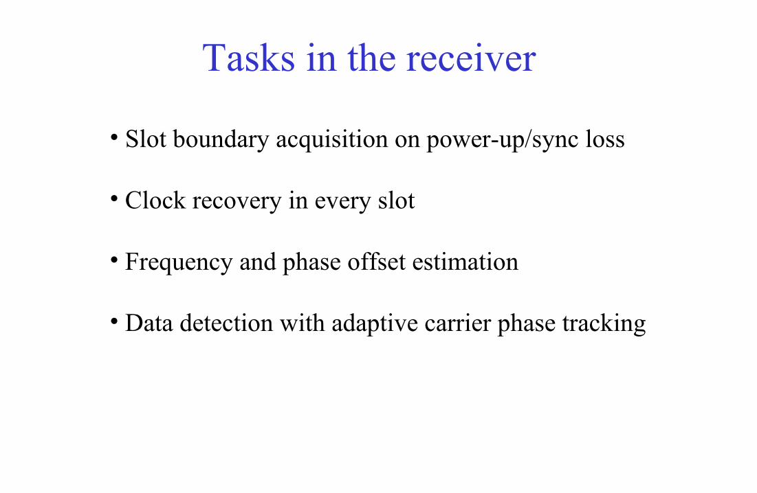
• Slot boundary acquisition on power-up/sync loss
• Clock recovery in every slot
• Frequency and phase offset estimation
• Data detection with adaptive carrier phase tracking
Tasks in the receiver

Signal Processing in Digital Domain
Symbol clockphase (kTb/12, k=0,1…11)
Coherent data detector with adaptive phase
correction
Carrier frequencyand phase offset
estimator
DemodulatedDPSK data
Start ofS-field
B-field
S-fieldonly
Bandpass samples
@ 3.456 MHz
Acq & Sync/data (for GFSK)
DigitalFM
demodulator
S & A fieldsB field (if GFSK)
DemodulatedGFSK data
@ 2.304 MHz
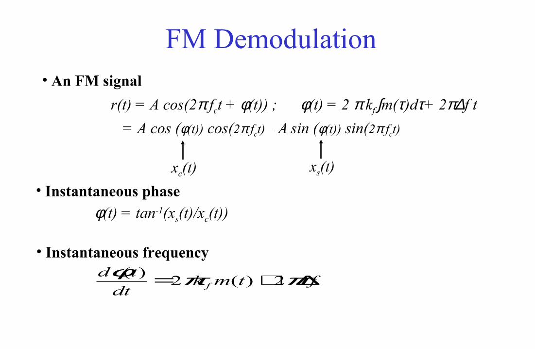
FM Demodulation
• An FM signal
r(t) = A cos(2π fct + φ(t)) ; φ(t) = 2 π kf ∫m(τ)dτ+ 2π∆f t
= A cos (φ(t)) cos(2π fct) – A sin (φ(t)) sin(2π fct)
• Instantaneous phase
ftmkdt
tdf ∆+= ππφ
2)(2)(
• Instantaneous frequency
φ(t) = tan-1(xs(t)/xc(t))
xs(t)xc(t)
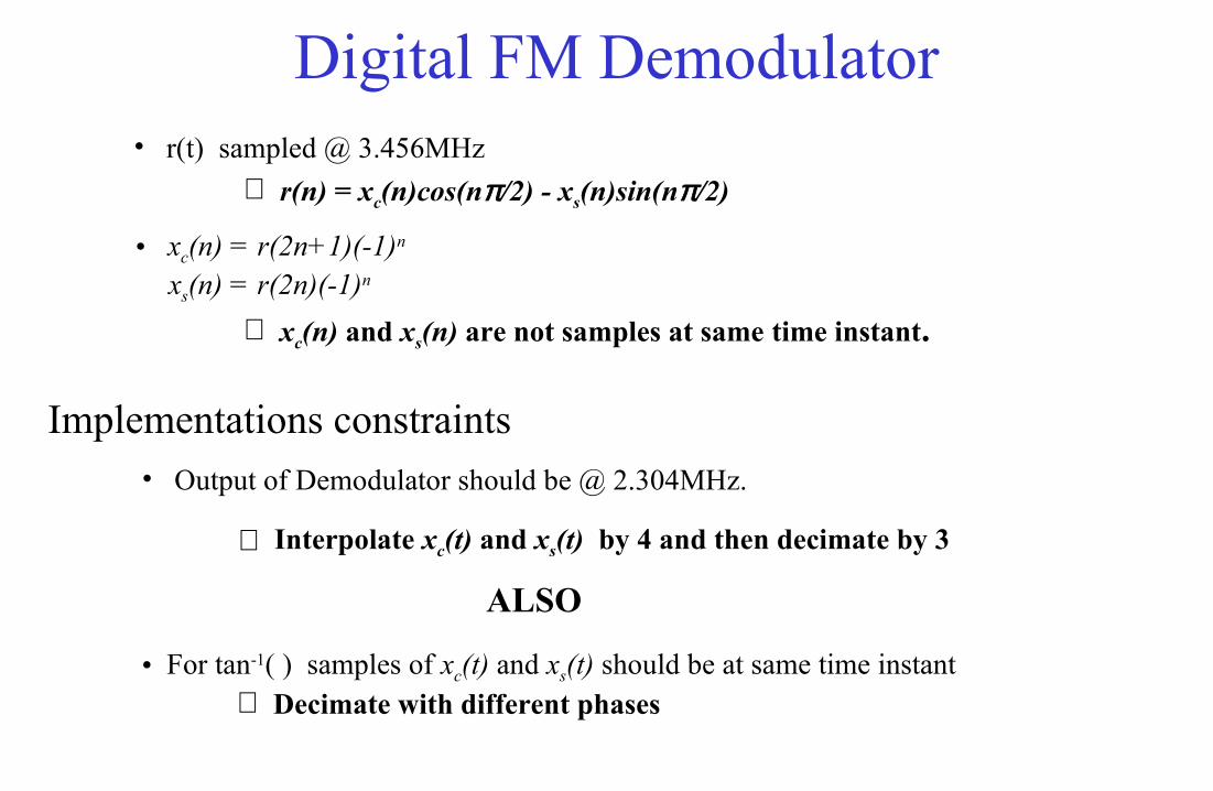
Digital FM Demodulator
Implementations constraints• Output of Demodulator should be @ 2.304MHz.
ALSO
⇒ Interpolate xc(t) and xs(t) by 4 and then decimate by 3
• For tan-1( ) samples of xc(t) and xs(t) should be at same time instant⇒ Decimate with different phases
⇒ r(n) = xc(n)cos(nπ /2) - xs(n)sin(nπ /2)
⇒ xc(n) and xs(n) are not samples at same time instant.
• xc(n) = r(2n+1)(-1)n
xs(n) = r(2n)(-1)n
• r(t) sampled @ 3.456MHz
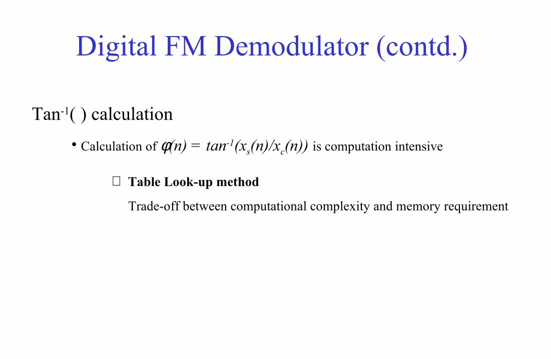
Tan-1( ) calculation
• Calculation of φ(n) = tan-1(xs(n)/xc(n)) is computation intensive
⇒ Table Look-up method
Trade-off between computational complexity and memory requirement
Digital FM Demodulator (contd.)
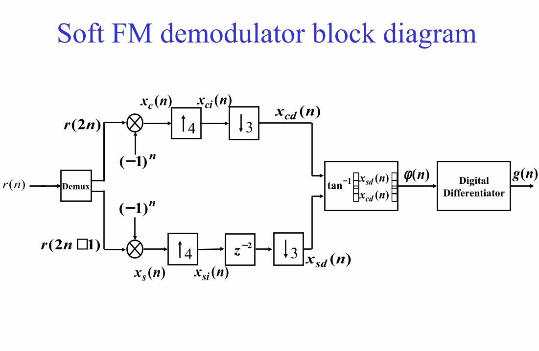
Soft FM demodulator block diagram
)12( +nr
)2( nr
)(nr Demux
)(nxc )(nxci )(nxcd
n)1(−
−
)(
)(tan 1
nx
nx
cd
sd)(nφ )(ng
DigitalDifferentiator
4 3)(nxs )(nxsi
)(nxsd
4 3
2−z
n)1(−

Signal Processing in Digital Domain
Coherent detector with adaptive phase
correction
Carrier frequencyand phase offset
estimator
Symbol clockphase (kTb/12, k=0,1…11)
DemodulatedDPSK data
Start ofpreamble
A and Bfields
S-fieldonly
Bandpass samples
@ 3.456 MHz
Acq & Sync/data (for GFSK)
DigitalFM
demodulator
S & A fieldsB field (if GFSK)
DemodulatedGFSK data
@ 2.304 MHz
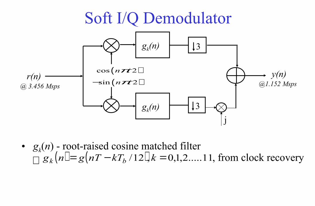
Soft I/Q Demodulator
r(n)
gk(n)
( )cos / 2nπ
( )sin / 2nπ−
gk(n)
y(n)@ 3.456 Msps @1.152 Msps
3
3
j
• gk(n) - root-raised cosine matched filter ⇒
( ) ( ) 11.....2,1,0,12/ =−= kkTnTgng bk , from clock recovery
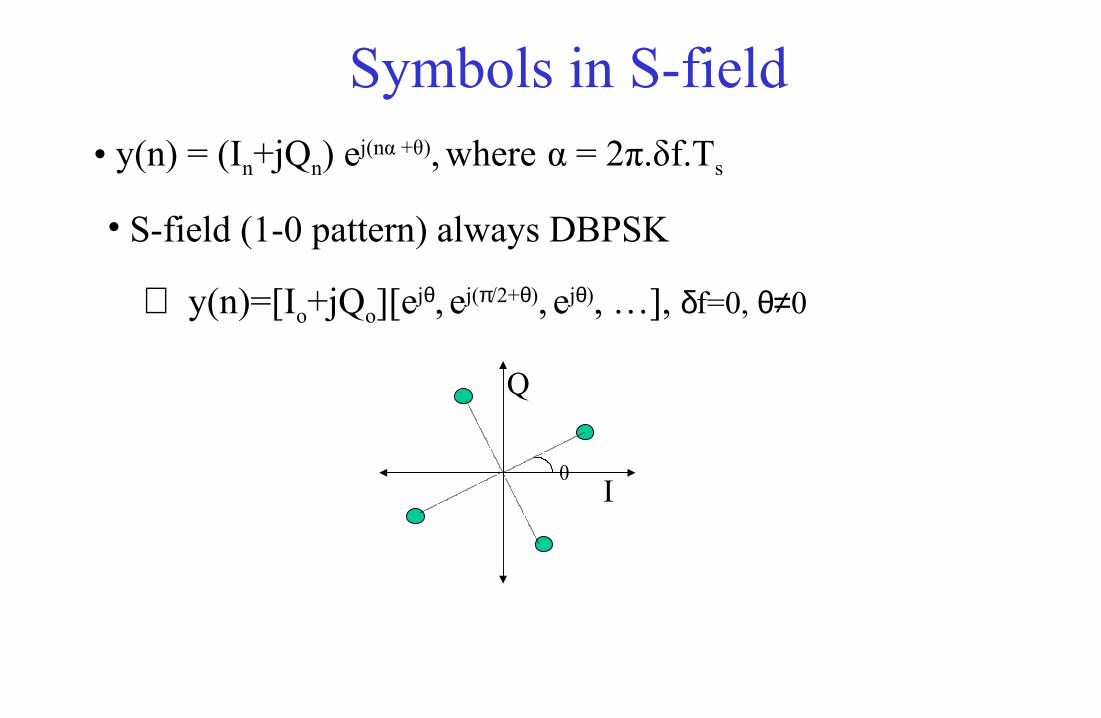
• y(n) = (In+jQn) ej(nα +θ), where α = 2π.δf.Ts
Symbols in S-field
• S-field (1-0 pattern) always DBPSK
I
Q
θ
⇒ y(n)=[Io+jQo][ejθ, ej(π/2+θ), ejθ), …], δf=0, θ≠0
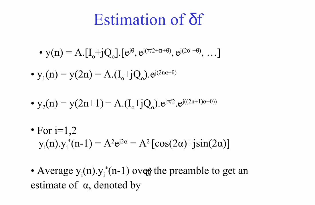
• y1(n) = y(2n) = A.(Io+jQo).ej(2nα+θ)
• y2(n) = y(2n+1) = A.(Io+jQo).ejπ/2.ej((2n+1)α+θ))
• For i=1,2 yi(n).yi
*(n-1) = A2ej2α = A2 [cos(2α)+jsin(2α)]
• Average yi(n).yi*(n-1) over the preamble to get an
estimate of α, denoted by
Estimation of δf
α̂
• y(n) = A.[Io+jQo].[ejθ, ej(π/2+α+θ), ej(2α +θ), …]

Estimation of θ• Compensate for δf
θθααα jnn
njnn
jnd ejQIejQIenyny ][][)()( )ˆ(ˆ +≈+== +−−
)12()12(
)2()2( 2/
+=+= −
nynz
enynz
de
jde
π
2/)12()12(
)2()2(πj
do
do
enynz
nynz−+=+
=
• Form two sequences ze(n), zo(n)
⇒ze(n)
⇒zo(n)
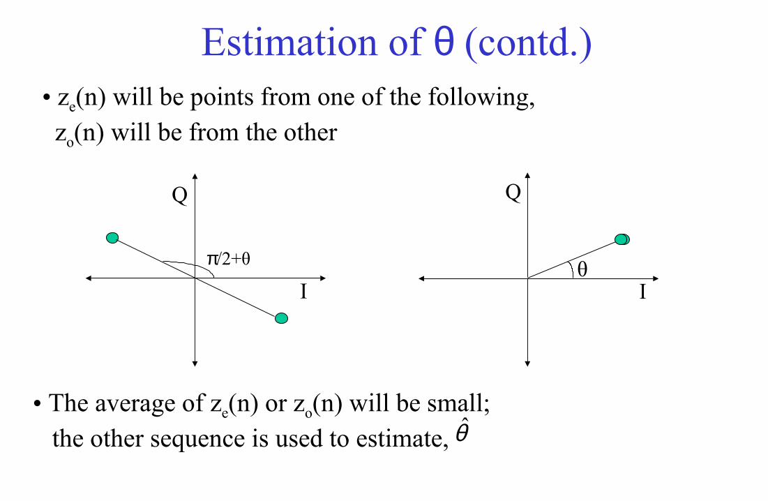
• The average of ze(n) or zo(n) will be small; the other sequence is used to estimate,
Estimation of θ (contd.)
θI
Q
• ze(n) will be points from one of the following, zo(n) will be from the other
π/2+θ
I
Q
θ̂
( )y n ( )d̂ n
( )*w n
e (n )
+_ˆˆ( . )e j n α θ− +
( )u n ( )v n
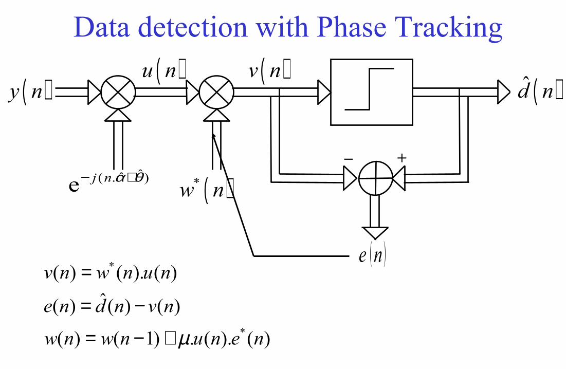
Data detection with Phase Tracking
ˆ( ) ( ) ( )e n d n v n= −*( ) ( 1) . ( ). ( )w n w n u n e nµ= − +
*( ) ( ). ( )v n w n u n=
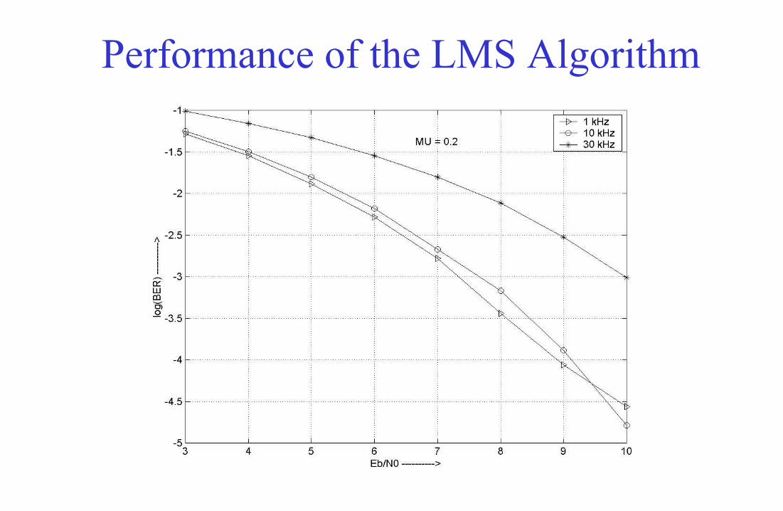
Performance of the LMS Algorithm
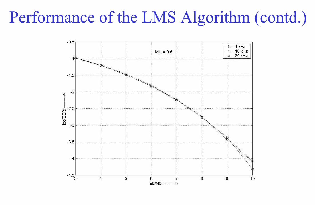
Performance of the LMS Algorithm (contd.)
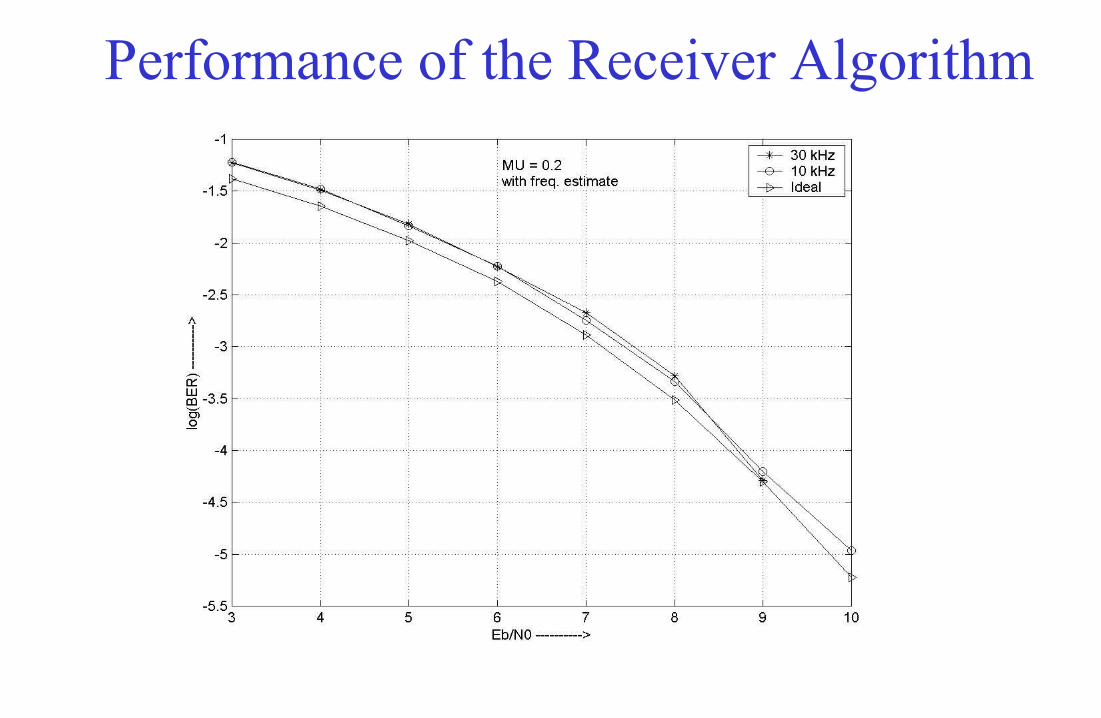
Performance of the Receiver Algorithm
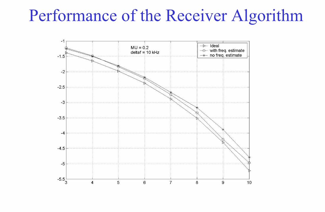
Performance of the Receiver Algorithm
Conclusions
• Transceiver hardware design for 3G DECT physical layer was presented
• Issues involved in the receiver design were discussed
• Carrier synchronization algorithms were discussed
• Performance results of the receiver were presented


