Reconfigurable Baseband Blocks for Wireless Multistandard Transceivers Department of Electrical and Computer Engineering Faculty of Engineering and Architecture American University of Beirut Final Year Project Spring 2005-2006 Advisors: Prof. Mazen Saghir Prof. Walid Ali Ahmad Members: Abdul Hadi Al-Sayed 200300531 Hasan Khalifeh 200301843 Houssam Hayek 200302327 Submitted On: 23.5.2006
Transcript
Reconfigurable Baseband Blocks for Wireless Multistandard Transceivers
Department of Electrical and Computer Engineering
Faculty of Engineering and Architecture American University of Beirut
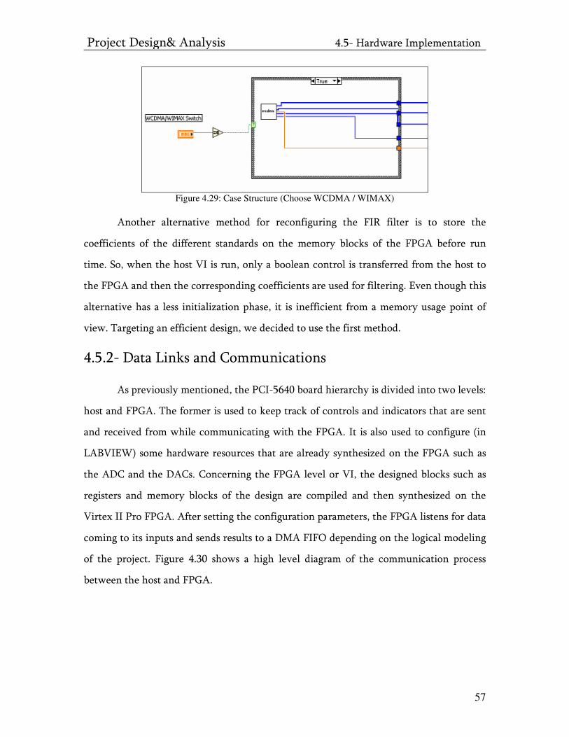
-Figure 4.29: Case Structure (Choose WCDMA / WIMAX) 57
viii
-Figure 4.30: Host-FPGA Link 58
-Figure 4.31: FPGA Read Process 59
-Figure 4.32: DMA FIFO Read Method 60
-Figure 4.33: FIR implementation Using Arrays and FIFOs 61
-Figure 4.34: Write a 32-bit coefficient in the memory 62
-Figure 4.35: Convolution Process 65
-Figure 4.36: HOST VI 66
-Figure 4.37: FPGA VI 67
-Figure 4.38: Frequency Domain of the Input WCDMA signal 70
-Figure 4.39: Frequency Domain of the Input WCDMA signal 70
-Figure 4.40: WCDMA Initial Constellations 71
-Figure 4.41: WCDMA Filtered Constellations 71
-Figure 4.42: Frequency Domain of the Input WIMAX signal 72
-Figure 4.43: Frequency Domain of the filtered WIMAX signal 73
-Figure A.1: Transposed FIR 82
-Figure A.2: Transposed FIR with multiplier block 82
-Figure A.3: High level FPGA_ I/O architecture 85
-Figure A.5: High level Diagram of the PCI 5640 85
ix
List of TablesList of TablesList of TablesList of Tables
-Table 4.1: MATLAB code to generate FIR coefficients of WIMAX 31
-Table 4.2: MATLAB Testing for Fixed Point Notation 63
x
AbstractAbstractAbstractAbstract
As new wireless communication standards are introduced to market, the idea of
reconfigurable systems is becoming essential to solve the different problems that the
coexistence of multiple standards poses. In this report, a proposed implementation
technique is given to reconfigure WIMAX and WCDMA transceivers. This
implementation technique highlights the design considerations related to the channel
FIR filter present in the receiver of each of the prementioned standards. This report, also,
discusses the features of PCI5640 Labview8.0 device on which the proposed design is
downloaded. In addition, a common architecture design is proposed in order to facilitate
future job of reconfiguring the different modules in the transceiver. Implementation,
performance, reconfigurable FIR filter testing, and results are further discussed in details.
1. Introduction
1.1- Problem Definition
1.2- Report Structure
Reconfigurable Baseband Blocks for Wireless
Multistandard Transceivers
Introduction 1.1- Problem Definition
2
1-Introduction
Since early 1980s, the evolution of new wireless communication standards has been
remarkably noticed, especially in migrating from analog communication systems to their
equivalent in the digital domain. Later, the industrial competition between Asia, Europe,
and America encouraged the development of a unique mobile system standardized all
over the world which would be of great benefit to the market [1]. From now till the
deployment of the above mentioned standard, the market will be facing many problems
due to the coexistence of multistandardized communication systems. Nowadays, many
researchers are working on short end solutions before the transition to the worldwide
standards takes place. One leading solution, the subject of our project, is the dynamic
reconfiguration of the different modules in the system to suit the specs of as many
standards as possible.
1.1- Problem Definition
Nowadays, the heterogeneity found at the different layers of wireless communication
channel is increasing as new standards are introduced. Despite this problem, many
countries such as European countries and Japan, are willing to install new base stations
that support multitude of communication standards such as GSM, EDGE, UMTS-FDD and
Bluetooth. Designing such base stations efficiently requires studying the reconfigurable
aspects of the different modules in order to avoid duplication of resources. Thus, the
system is capable of dynamically reconfiguring itself to the environment as needed. This
solution is beneficial for both, to the final user and the manufacturers. Starting with the
end user, he will benefit from a higher quality of service, better connectivity, and
enhanced roaming concept. Concerning the manufacturers, they would profit from ease
of introduction of new types of services, less to market time and reduction in the cost of
addition of new standards.
Introduction 1.2- Report Structure
3
In this report, we present the design and implementation of some blocks of a
reconfigurable transceiver that is adaptable to WCDMA and WIMAX.
1.2- Report Structure
Our report is organized as follows. Chapter 2Chapter 2Chapter 2Chapter 2 introduces our topic by giving a general
survey about the related subjects in our design; an overview of WIMAX, and WCDMA
wireless standards, with their specifications, is given. A general introduction about SDR
concept comes afterwards. FIR filters and FPGA related topics are followed. . In chapter chapter chapter chapter
3333, different design alternatives that were studied throughout our survey are presented. A
more detailed description of our system design and analysis, including simulation and
hardware implementation, is then introduced in chapter chapter chapter chapter 4444. In this chapter, we also go
further by presenting our testing scheme used and a detailed description of the results
obtained. In chapter chapter chapter chapter 5555, we present system design constraints form different perspective
such as economic, social, sustainability, political… Finally a conclusionconclusionconclusionconclusion section is added.
An appendix appendix appendix appendix covering further details about the fixed point notation, the PCI 5640, area
considerations in FIR design, Virtex II pro FPGA capabilities and filter coefficients design
is included for further information.
System Design Constraints
2. Literature Survey
2.1- Overview of Proposed Wireless Standards 2.1.1- WIMAX
2.1.2- WCDMA
2.2- Software Radio Concept
2.3- FIR Filters 2.3.1- Variable FIR Filters 2.3.1.1- Design Methods for Variable FIR Filters
2.3.1.2- FIR Tap Design With Variable Frequency Response
2.3.2- Area Considerations in FIR Design Schemes 2.4- Hardware Platforms 2.4.1- FPGA features
2.4.2- LABVIEW 8.0 System Board: PCI 5640
2.5- Error Vector Magnitude (EVM) Metric
Reconfigurable Baseband Blocks for Wireless Multistandard Transceivers
Literature Survey 2.1- Overview of proposed Wireless Standards
5
2- Literature Survey
In this chapter, we present a literature survey about some topics needed for the design
and implementation of the final year project. An overview the proposed 3G wireless
standards: WIMAX and WCDMA including their specifications is presented. A general
description of the software radio concept (SDR) is also introduced. A survey about FIR
filters, in particular variable FIR filters and some design related techniques follows.
Finally, we present the features of the used Virtex-II Pro FPGA as well as the definition
of the used Error Vector Magnitude (EVM) metric.
2.1- Overview of Proposed Wireless Standards
Due to the evolving technology, users’ needs are becoming more crucial, especially in
the field of wireless communication. He no more feels sufficient to use his mobile phone
for voice communication, but also looks forward for high data rata communications
through SMS or even multimedia communication. For all these reasons, new wireless
standards evolved in order to meet such and other user’s requirements. Of these
standards, we mention: WIMAX and WCDMA.
2.1.1- WIMAX
WIMAX, (Worldwide for Microwave Interoperability Access) also referred to as
802.16, is the current standard for Broadband Wireless MAN networks that is aimed to
provide a wireless alternative to cable, DSL and T1/E1 for last mile broadband access. It
will be also used to connect hot-spots to the internet [2]. It has the potential for very long
range (5 - 30 miles) and high speeds [3]. The first version of WIMAX was approved as an
IEEE Standard 802.16-2001 and this was published in 2002. This standard, however, had
the drawback of addressing only fixed line-of-sight connections by focusing on licensed
Literature Survey 2.1- Overview of proposed Wireless Standards
6
frequencies in the range of 10-66 GHz; this standard could reach a maximum distance of
5 Km [2].
Because of the mentioned drawbacks, they had to enhance the current standard thus
leading to a new standard 802.16a that addresses lower frequencies 2-11 GHz range; it
could reach a maximum distance of 50Km (ten times better) with a bit rate up to
75Mbit/s. The most important advantage for this standard, in addition to the previous
mentioned ones, is the fact that it supports Non-line-of-sight. This is because this
standard runs on lower frequency bands in comparison to the high frequency bands
involved in the previous standard (10-66GHz) [2].
WIMAX has a higher capacity with a lower cost than DSL or any cable for extending
fiber networks. It also has the advantage of supporting multimedia and fast internet
applications. The block diagram of 802.16a is illustrated in figure 2.1.
Figure 2.1: WIMAX Block Diagram
As shown in the above diagram, the WIMAX uses OFDM and this provides the possibility
of using NLOS (no line of sight) systems as deduced [2].
WIMAX specifications are summarized below:
- Selectable channel bandwidths of 1.5, 1.75, 3, 3.5, 5.5, 7, 10, 14 and 20 MHz
Literature Survey 2.1- Overview of proposed Wireless Standards
7
- 256 – point FFT / IFFT
- 10-bit AGC with fully programmable outputs for interface to any type of attenuator.
- Supports maximum 128dB of attenuation with 1⁄2 dB step resolution.
- Includes interpolation and decimation filters for 2x oversampling
Moreover, the filter characteristics depend on the ADC (Analog to digital converter)
dynamic range and sample rate [5].
It is useful at this step, to explain some of the blocks that appeared in the figure above:
Convolutional EncoderConvolutional EncoderConvolutional EncoderConvolutional Encoder: This encoder encodes a stream of binary input vectors (K) and
outputs a, usually, larger stream of output vectors (K*L) where L is a certain positive
integer chosen suitably for the design specifications [4]. This encoder plays an important
role in a fading, or noisy, environment because it is capable of correcting some errors
affected by such environment.
Interleaver: Interleaver: Interleaver: Interleaver: This block improves further the performance of encoder at the transmitter
side and decoder at the receiver side [4]. Its presence becomes more important in a fading
environment where it spreads the errors into many (K*L) output bits thus leaving few
errors in each (K*L) output bits and thus is capable of correcting these few errors.
Modulator: Modulator: Modulator: Modulator: It (802.11a) uses OFDM (Orthogonal frequency division multiplexing) where
it divides the given bandwidth into many multicarriers and sends the data (for one user
or multiple users) on each multicarrier. It uses shifted pulse shaping filters at transmitter
and receiver. This would filter some crossings between the multicarriers [4].
Time guard: Time guard: Time guard: Time guard: This block is added to improve the modulator more by decreasing the effect
of multipath propagation. Accordingly, OFDM needs only one multiplication on each
subcarrier as equalization [4].
Puncturer: Puncturer: Puncturer: Puncturer: This block decreases the rate of bits to match the rate of the interleaver in
such a way, it won’t loose any information.
Literature Survey 2.1- Overview of proposed Wireless Standards
8
2.1.2- WCDMA
Wideband CDMA is a third-generation (3G) wireless standard. It uses a 5 MHz
channel for both voice and data, offering an initial data speed of 384 Kbps [3]. It can also
reach speeds of up to 2 Mbps for voice, video, data and image transmission.
WCDMA is also referred to as UMTS - the two terms have become interchangeable [3].
This standard is based on code division multiple access modulation (CDMA) which
provides the capability of finding multi-user scenarios. However, this leads to inter-
symbol and intra-symbol interference (ISI). Thus, it uses a spread spectrum modulation
technique (SS) that is capable of reducing interference by a factor “L” called “the
spreading gain” or the “spreading factor”. Actually, this modulation technique has other
advantages. For example, it spreads the signal into a larger bandwidth with same energy,
(thus reducing the amplitude of the signal) and accordingly, it can escape any voluntarily
jamming action that has a certain noise threshold (the information signal will lie below
this threshold). Also, this technique enables for multiple accessing for the same frequency
band and at the same time. This, however, leads to some problems, especially,
interference which can be solved by some techniques that are implemented by the
WCDMA like: Soft handover, and softer handover solution techniques. The WCDMA
block diagram is shown in figure 2.2.
As shown in the figure 2.2, the mapping used is a QPSK mapping which maps every
two bits into one symbol. Upsampling is then performed, usually by a factor of 4, to
increase the bit rate. Upsampling is performed so that we can input the output of our
processing blocks at the same rate to the DAC to be processed correctly [6].
Upsampling is performed by inserting (4-1) zeros between each original input and the
net result would be a compressed DTFT signal by a factor of 4 [7]. However, Upsampling
adds to the original signal undesired spectral images which are centered on multiples of
the original sampling rate. Accordingly, we have to perform some kind of filtering to
Literature Survey 2.1- Overview of proposed Wireless Standards
9
remove the undesired spectral images (this is the interpolation filtering at the end of the
chain) [6].
Figure 2.2: WCDMA Block Diagram
The standard uses a root raised cosine filter (RRC) which has the characteristic, in
addition to being a pulse shaping filter, of canceling ISI in an ideal channel scenario since
the peak of only one of the signals will lie above the zero crossings of all the other signals.
This means that all the other signals will have no impact on this single signal and thus it
will not suffer from ISI. The FIR root raised cosine time function is given in Figure 2.3.
The function obeys the following equation:
Where α is the rolloff factor.
2
(1 ) (1 )cos sin
4 4( )
41
t T t
T t Th t
T
T
α π α π
α α
π α
+ − +
=
−
Literature Survey 2.1- Overview of proposed Wireless Standards
10
Figure 2.3: Ideal root raised cosine filters
Upcoversion is then followed. It converts the low frequency signal into an RF
frequency signal. A filter is then applied called “interpolation filter”, this filter, as
discussed previously, removes the undesired spectral images caused by upsampling and
upconversion. The output has then the same rate as the DAC and accordingly, it can now
be inputted to the DAC block and then transmitted.
The receiver components contain the inverse of the blocks explained previously.
Literature Survey 2.2- Software Radio Concept
11
2.2- Software Radio Concept
In the transformation from 2G to 3G standards, we need a common implementation
platform which can group all wireless standards in one way or another.
One evolving technique for the variable FIR implementation is using the SDR concept.
“SDR is a rapidly evolving technology that is receiving enormous recognition and
generating widespread interest in the telecommunication industry. It is the focus of
research in the communication field world wide” [8].
“SDR refers to the technology where software modules running on a generic
hardware platform are used to implement radio functions” [8, 9]. In other words, the
hardware platform supports multiple software modules. So the system can switch
between different standards by running the corresponding software.
SDR tries to achieve two main goals [10].
-to move the digital part of the transmitter and the receiver as much as possible
toward the antenna (RF end)
-to replace ASIC with DSPs since DSPs are able to process baseband signals and thus
radio functionalities through software
As illustrated above, most solutions are trying to rely on software to solve different
problems. These solutions, however, need not be the optimal ones. In addition to
software, hardware programmable devices such as FPGAs need to be used in parallel to
reach optimal performance.
SDR offers many advantages to the user, the most important of which is
reconfigurability. The Reconfigurability subject has been extensively researched in the
last decade especially in the field of mobile communications. Different people have been
working on reconfiguring the different modules of the channels. For example in [11], the
paper presents the implementation in software of the different modulation/demodulation
schemes for the GSM, UMTS, EDGE and Bluetooth on a unique hardware platform.
Looking into these schemes, UMTS uses QPSK as modulation technique, GSM – GMSK,
Literature Survey 2.2- Software Radio Concept
12
EDGE - 8PSK, Bluetooth-GFSK. The need to implement these different systems on the
hardware platform forced the researchers to look into the mathematical representation of
these types of modulation. They observed that all these modulation schemes can be
expressed by a quadrature decomposition, which encouraged them to build a common
architecture called digital-IF. Their implementation is totally done in software and is
download on a DSP, also the transition in the frequency band is done in software. This
implementation takes advantage of the common mathematical aspect of the different
modulation schemes and benefits from DSP board that allows work to be done in the
software domain.
More advantages can be offered by SDR. These include “Multi service”; the SDR
system can theoretically operate in multi-service environments, without being
constrained to a particular standard, “Multi band”; SDR systems can theoretically
function on any radio frequency band, “Update Feature”: the software modules that
implement new characteristics can be downloaded to the hardware platform and thus the
system can be kept up to date [1,8,12,13].
Some drawbacks of SDR is that the system can have higher power consumption,
higher processing power (MIPS) requirement or higher initial costs depending on the
design.
Literature Survey 2.3-FIR Filters
13
2.3- FIR Filters
The digital filter is one of the basic blocks in Digital Signal Processing and
Communication systems. Their design and thus their operation can affect the
performance of the whole system. FIR Filters are characterized by several parameters
including their orders and the values of their coefficients which depend on the desired
frequency response. Generally, there are two kinds of digital filters: IIR and FIR. Infinite
Impulse Response, IIR, Filters are filters whose impulse response can be infinite in
duration. Finite impulse response filter, FIR, on the other hand, is a special kind that
contains a finite number of taps in its impulse response [14, 15, 16]. It is one of the most
widely used modules in DSP applications. “It performs a moving, weighted average on a
discrete input signal, x(n), to produce an output signal” [17]. Thus, the FIR output
depends only on the previous N inputs; where N is the number of taps.
The basic operation in the filtering process is to convolve the input by the filter weights
or taps as given by the following equation:
0
( ) ( ) ( )N
k
y n x n h n k=
= −∑ (1)
Fig 2.4 shows the architecture of a standard fully pipelined FIR filter for the
implementation above formula.
Figure 2.4: Standard FIR Filter
FIR filter design involves two main stages: coefficients design and architecture design.
The following section deals with the first stage: coefficients design. The second stage,
architecture design, is referred to in the FIR Implementation section. For more
Literature Survey 2.3-FIR Filters
14
information about the first stage, the filter coefficients design, refer to section I in the
Appendix. As for the second stage, the FIR implementation stage, it is illustrated in
chapter 3 in the report, Project design and analysis.
2.3.1- Variable FIR filters
Variable digital filters are digital filters whose frequency characteristics depend on
control or tuning parameters. The most common variable parameters include:
•••• Variable cutoff frequency
•••• Adjustable Passband Width
•••• Adjustable Stopband Width
•••• Controllable Fractional Delay
•••• Magnitude and number of ripples
•••• Attenuation level in various bands
Varying any of the above parameters results in a change of the order of the filter i.e. the
number of taps or coefficients of the filter and of course their values.
2.3.2.3.2.3.2.3.1111.1.1.1.1---- Design Methods for Variable FIR Filters Design Methods for Variable FIR Filters Design Methods for Variable FIR Filters Design Methods for Variable FIR Filters
Methods for designing variable digital filters can be classified into two main
categories: the transformation based methods and the spectral parameter approximation
methods [18]. The transformation methods are based on first designing a filter with
certain fixed frequency characteristics and then applying a certain transformation to
obtain the new filter with new desired frequency characteristics based on predesigned
parameters. Generally, this method is applied to filters with variable cutoff frequencies.
The spectral parameter approximation methods, on the other hand, approximate either
the impulse response or the poles and the zeros of the filter by polynomials that are
functions of certain spectral parameters [18, 19, 20, 21]. One used technique is the curve
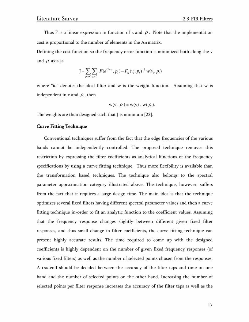
fitting technique as shall be examined in the following section.
Literature Survey 2.3-FIR Filters
15
2.3.1.2- FIR Tap Design with Variable Frequency Response
Different approaches for each category have been proposed for the design of digital
variable filters taps. In this paper, we try to focus on the most widely used approaches.
One old but still evolving technique that belongs to the second category expresses the FIR
impulse response as a linear combination of some basis functions. Another technique
relies on the Frequency masking concept. Note that the frequency masking approach is a
mix of the two categories as will be illustrated later.
In the former, each filter coefficient is a multidimensional function or polynomial of the
spectral parameter. The famous algorithms for the optimal approximation of filter
coefficients include the LSE (least squares method), the WLS (weighted least squares) and
4.4.2.14.4.2.14.4.2.14.4.2.1---- WIMAX WIMAX WIMAX WIMAX ChannelChannelChannelChannel FIR Filter Design FIR Filter Design FIR Filter Design FIR Filter Design
4.4.2.24.4.2.24.4.2.24.4.2.2---- WCDMA Channel FIR Filter Desi WCDMA Channel FIR Filter Desi WCDMA Channel FIR Filter Desi WCDMA Channel FIR Filter Designgngngn
After conducting a literature survey, we move to the design and analysis phase.
The chapter presents the details of the system definition, the design of the variable FIR
filter, the performed simulations, the reconfigurable architecture, as well as the hardware
implementation and the project assessment.
4.1 System Definition
Our system is primarily a reconfigurable transceiver supporting two of the 3G
standards: WCDMA and WIMAX standards. The transceiver is optimized to support
these two standards that include different modules in their channels. Initially, we studied
each scheme alone by looking into its channel and requirements, and then we tried to
build a common architecture where we emphasize on the idea of reconfiguring the
common modules like channel filers, pulse shaping filters, modulation on both sides from
the transceiver. This reconfigurability scheme helps in developing new systems that
supply the designer with both flexibility of design as well as less hardware resources,
especially that the hardware platforms used in such implementations have limited
resources. For example, implementing three different FIR channel filters would require
the use of 3n multipliers, instead of n multipliers for one reconfigurable filter. The
hardware platform used in our project is PCI 5640 IF RIO system board, manufactured by
National Instruments. This board is typical for our design providing us with high data
rates, AD and DA converters, and the Virtex II-PRO v3000 FPGA. Our system has two
types of inputs: the control/switch, to choose between the two used standards, and the
data input port which receives a sequence of I & Q modulated values representing a given
message sent over one of these standards. At the output side, we get another set of I & Q
values and we would be targeting a low EVM degradation.
Project Design& Analysis 4.2- FIR Filter Coefficients Design
29
4.2- FIR Filter Coefficients Design
This section discusses the design of an FIR filter, in terms of order and coefficient
values design. First, however, we define the FIR system and then move to the generation
of the filter coefficients for the WCDMA and the WIMAX channel filters.
4.2.1- FIR System Definition
A reconfigurable FIR filter, supporting WCDMA and WIMAX standards, with a
variable frequency response is proposed. This reconfigurability aspect has the vivid
advantage of removing some extra unneeded hardware. Our system is part of a larger
system aiming to adapt itself to a large variety of wireless systems, already standardized,
by means of a common hardware platform. We will first generate the different impulse
responses of the different filters using MATLAB. Then, we will use the Virtex-II V2MB
1000 system board as the hardware platform for our system. We will instantiate different
hardware blocks on the system board including the interrupt controller (choose type of
signal), BRAM memory (storing coefficients), on-chip multipliers …and then connect the
different components to come up with the whole system. Our system includes control as
well as data inputs. In-order for the filter to be able to distinguish between the different
proposed standards, the system checks a boolean control: TRUE for WCDMA and FALSE
for WIMAX. The data input is the “InputSignal”, sequence of I & Q values that need to be
filtered. Based on the control, it then uses the corresponding response in the convolution
process. The output for our system is the “OutputSignal” is the filtered values.
4.2.2- Filter Coefficients Generation
The filter design is mainly divided into 2 steps: order and coefficients. The order of
the filter varies according to the specs. In order to achieve certain specs, there is a
minimum order that we need to satisfy to get an acceptable frequency response.
Increasing the order above this target will lead to a more sharp response, but we will pay
Project Design& Analysis 4.2- FIR Filter Coefficients Design
30
for the delay and hardware usage. First, we wrote a MATLAB function that generates the
required order of the filter, generate its coefficients, and then plots its frequency response
based on the rejections in the different bands and the pass-band as shown in Table 4.1.
We also used the FS_10 program to generate the FIR filter coefficients and compare them
with those generated by the MATLAB simulation. In the subsequent section, we generate
the FIR coefficients for the WIMAX standard. Coefficients for the WLAN can be
similarly generated and shall be included in the spring final project report.
4.2.2.1- WIMAX Channel FIR Filter Design
Section 2.1.1, WIMAX standard specification, presents the different bit rates that
WIMAX can support. Of these bit rates, we consider an RF bandwidth of 7 MHz. That is,
the WIMAX can send a data rate up to 7 Mbits/sec at RF. Accordingly, at baseband the
bandwidth of the WIMAX signal will be 3.5M1. [5] presents the FIR baseband
specifications of WIMAX. Based on these specifications, we wrote a MATLAB code to
generate the FIR coefficients as shown in table 4.1. The order of the filter came to be 52.
Figure 4.1 shows the corresponding frequency response of the WIMAX FIR filter. As you
notice, the center frequency is approximately 3 MHz and the specs are met.
% The WIMAX has a bandwidth of 7MHz at RF frequency. Therefore, at baseband, it % has a bandwidth of 7/2 = 3.5MHz. At Adj. Ch (7MHz), the attenuation is at least % 38dB. At Alt. Ch (14MHz) the attenuation is at least 57dB freq_band =[0 2000 3500 7000 14000 16000]; % define the frequency bands of WIMAX attenuation_dB = [0 0 -38 -57]; % define the attenuation at each band in (dB) attenuation = 10 .^(attenuation_dB/10); % transform the attenuation into linear scale Ripple_Ratio = [0.001 0.001 0.001 0.001];% define the percentage ripple at each band Sampling_Frequency = 32e3; % the sampling time is given by ADS to be 0.03125us [N,fpts,mag,wt]= firpmord(freq_band,attenuation,Ripple_Ratio,Sampling_Frequency); b = remez(N,fpts,mag);% apply the remez algorithm given the order % and frequency bands with their attenuations [H,f]=freqz(b,1,512); plot(f/pi*11500,20*log10(abs(H))) axis([0 10000 -100 1]) xlabel('Frequency (Hz)'); ylabel('Attenuation (dB)') title('FIR Baseband filter of WIMAX')
1 7M/2
Project Design& Analysis 4.2- FIR Filter Coefficients Design
31
Table 4.1: MATLAB code to generate FIR coefficients of WIMAX
Figure 4.1: WIMAX FIR baseband filter
To validate our results, the specs were supplied to the FS10 program as shown in
Figure 4.2. The sampling rate is 32 MHz, the same value used by the MATLAB code. This
is also true for the order of the filter and the center frequency. Figure 4.3 shows the
corresponding frequency response, which came to be as expected. The only difference is
the presence of higher amplitude ripples which are characteristic of the built in function
of the program. The group delay, also shown in the figure, is constant. This implies a
linear phase filter, a common characteristic of FIR.
Figure 4.2: FS10 WIMAX FIR
Project Design& Analysis 4.2- FIR Filter Coefficients Design
32
Figure 4.3: WIMAX FIR Filter Response using FS10
4.2.2.2- WCDMA Channel FIR Filter Design
The WCDMA signal is a wideband signal of bandwidth 3.84MHz at radio frequency.
Accordingly, at baseband frequency, the cutoff frequency is 1.92MHz. [26] specifies the
baseband filter specifications of WCDMA. Following the same procedure as the one in
the previous section, the order of the filter turned out to be 48 with the frequency
response shown in figure 4.4. As shown in the figure, the cutoff frequency is
approximately 1.92MHz at -3dB value. This frequency response looks very similar to the
one shown in figure 4.5 which is simulated using the FS10 program. Again the group
delay is constant.
Project Design& Analysis 4.2- FIR Filter Coefficients Design
This degradation is also higher than the obtained one from the simulation which is
3.12%. We should mention that the value of the EVM in the case of the WIMAX is
higher than the one for WCDMA because the transmitter part from the WIMAX channel
does not include a pulse shaping filter as in the WCDMA case, especially that the pulse
shaping filter plays a major role in well distributing the constellations, so reducing the
EVM value. Concerning the frequency domain representation of the input signal and the
output signal are represented in figures 4.42 and 4.43 respectively. We easily notice that
the transition phase in PSD, shown in figure 4.42, is shopped off as seen in figure 4.43.
Figure 4.42: Frequency Domain of the Input WIMAX signal (Amp vs. Freq)
Project Design& Analysis 4.6- Project Assessment
73
Figure 4.42: Frequency Domain of the filtered WIMAX signal (Amp vs. Freq)
After presenting our results, we believe that the LABVIEW simulation and the
hardware implementation have reached quite similar results with some differences in the
case of EVM in favor of the simulation and the frequency response in favor of the
hardware implementation. So, implementing a reconfigurable FIR filter on an FPGA is a
good option and it would be able to compete with the implementation of any other type
of FIR filters.
CH 5: System Design
Constraints
Reconfigurable Baseband Blocks for Wireless
Multistandard Transceivers
System Design Constraints
75
5- System Design Constraints
For any project, designers should be down to earth and try to face as many constraints
as possible that their system poses and at any level, ranging from economical levels,
passing through social, political and ethical levels and ending with more technical
constraints; like manufacturability and sustainability.
Actually our project is a very important step towards achieving a uniform global
system, which although has different languages of communications within it (WIMAX,
WLAN, WCDMA, GSM, etc…) there would exist a unique communication language
capable of connecting all such non-uniform standards. Accordingly, there will be no
more a need for the present so called “Roaming Service” which is a relatively costly
service. Therefore, economically, there would be huge savings due to the absence of such
service on one hand especially for business men who keep traveling from one region to
anther. On the other hand, such reconfigurable system has the vivid advantage of
reducing hardware resources and adapting to different standards.
However, such system poses some economical constraints. This might be due to the
fact that since this reconfigurable system has to group multiple standards together, base
stations and mobile systems or any wireless card have to install new wireless blocks such
as switches (to switch between these reconfigurable standards) or blocks to remove any
possible RF coupling between these signals; such blocks are not needed in the case of a
single wireless standard device.
Socially, our project would help increase the social activities between different
cultures because it would allow people from different regions using different
communication standards to communicate with each other at low costs. Moreover, this
would lead to a decrease in the price of the international calls, thus parents can easily
contact their relatives and keep track of their news.
System Design Constraints
76
Also, the manufacturing process would take a long time to be processed especially
that installing a reconfigurable hardware design on today cell phones and base stations
would take a long time. This transition phase between these two generations is going to
affect the huge advancement in the latest facilities and applications integrated in our
phones such as cameras, video streaming… because the research in this phase would be
mainly concentrated on building area and power efficient reconfigurable blocks. So, as a
result, this transition includes a kind of trade-off between unifying the world and having
a low development rate in design and facilities.
Our project would be a typical competitor to roaming services by replacing them with
very low costs. But, this would create an issue of security since communications between
different countries would be allowed without sufficient level of control which may pose
its own effect especially nowadays where many countries have been encouraged by
globalization to dominate others.
Projecting the issue of security, discussed previously, on an individual bases may lead
to some of the undesirable ethical consequences. Again, people may take advantage of
this new system to spy other systems and you can imagine in what such unethical act
would result and to whom it might be directed if this subject was not solved. For this
serious problem, there needs to be a sufficient attention given to this issue and its effects
need to be seriously considered and dealt with.
Concerning sustainability, our project imposes a common hardware platform on
which any new standard can be integrated. However, this wouldn’t be applicable for new
highly developed standards especially if they follow a complete different architecture.
Thus, two possibilities are left for our reconfigurable design, either to survive with
present standards on behalf of the new ones, or undergo major changes in its architecture
to support the new standards; surely this would lead to sacrificing some old ones.
77
ConclusionConclusionConclusionConclusion
The objective of our FYP project is to give a solution to the problem that the
commercial wireless communication industry is currently facing due to the different
link-layer evolution steps that each wireless standard has undergone. This existence, in
many countries, of incompatible different wireless network technologies, ranging from
2G to 4G, has imposed many difficulties in the deployment of global roaming facilities
and problems in rolling-out new features or services due to the presence of wide-spread
legacy subscriber handsets [26]. Our project concept promises to solve such problems by
implementing the radio functionality as Software modules (using LABVIEW) running on
a generic hardware platform, the PCI5640 Labview8.0 board.
We started with a general overview of the design by giving a literature survey about the
related subjects such as FIR, SDR, EVM etc… We have seen some proposed
reconfigurable, common, architectures and, more importantly, our proposed
reconfigurable block diagram for WIMAX, and WCDMA, in a noisy environment, is
introduced. We have simulated the WCDMA and WIMAX chains using LABVIEW to
have a theoretical reference for our implementation. Moreover, FIR design was
established, and most importantly a reconfigurable FIR module was implemented on the
PCI5640 Labview8.0 board. The results were quite pleasing especially when compared
with the theoretical outcomes resulted from LABVIEW simulation. There was a small
difference between EVM degradation of both the simulation and implementation which
proves the validity of both our design and implementation.
We believe that such project is a very important step towards achieving a whole
reconfigurable transceiver. Therefore, we suggest for future FYP students to continue
where we stopped and try to reconfigure the other blocks in the whole channel
transceiver.
Appendix I- Digital Filter Coefficients Design
78
APPENDIAPPENDIAPPENDIAPPENDIXXXX
I- Digital Filter Coefficients Design
Filter coefficients can be designed using an automated tool, a software application that
generates the taps based on various user-defined parameters. One example of such tools is
the “FS10.0” software or the “Filter Solutions 10.0”.
The following algorithm explains the tap design of an FIR filter. The frequency response
for FIR filters is periodic in the frequency domain with a period of sampling frequency.
Since it is periodic, it can be represented by a Fourier series as shown below:
∑∞
−∞=
Ω−Ω =k
jKjekheH ).()(
where h(k) are the impulse response coefficients that describe the digital FIR filter [16].
These coefficients can be determined from the frequency response using the following
equation:
Ω= Ω
+Ω
−Ω
Ω
∫ deeHnh jjo
o
π
π
ππ
).(2
1)(
Notice the finite number of coefficients given in the above formula. The chosen number
of coefficients (N) should be chosen according to time delay and implementation cost.
The indices above range between –M and M and accordingly, we are assuming the
number of coefficients is equal to N = 2M+1. By making this selection, we are effectively
setting all other coefficients to zero [15].
The frequency response can be determined using the following formula:
∑∞
−∞=
Ω−Ω =n
jnjenheH ).()(
Plotting the desired frequency response and the one based on the designed coefficients
allows us to check if the design is acceptable. Thus, the user can adjust several
Appendix I- Digital Filter Coefficients Design
79
parameters: allowed ripple, transition band … and accordingly increase or decrease the
number of taps that implement the filter [15].
Appendix II- Area Considerations for Variable FIR Design
80
II-Area Considerations for Variable FIR Design
As mentioned in section 2.3.2, there exists a never-ending demand for decreasing the
amount of hardware used in a system. This leads to substantial benefits like reduced cost
and power consumption, increased application functionality1, and thus increased
utilization of FPGA resources …
In most FIR implementation, hardware consumption is mainly due to the multiplier
blocks rather than adder modules [23]. Different algorithms have been proposed for
efficient implementation of multiplier blocks. Previously, different algorithms were
proposed for minimizing adder hardware cost since it was assumed that the adder cost
dominates the area requirement; from a VLSI point of view. However, after the
introduction of the FPGA as the hardware platform, the solution of minimizing adders’
complexity does not work anymore since the “FPGA has a fixed architecture for
implementing digital logic”. Instead, it is the architecture design that minimizes such cost
[23].
Different commonly used approaches and architectures that increase resource
utilization are considered below:
Consider first the standard FIR implementation shown in figure 2.4. The figure shows a
full parallel, fixed coefficient FIR filter. For each tap, the filter requires one multiplier,
one adder and one delay element. Thus the resource usage is proportional to the number
of coefficients [14, 24, 25].
Other enhanced architectures and techniques with higher complexity include array
multiplication, multipliers using add and shift operations, transposed FIR, transposed FIR
architecture with multiplier block, MAG (Minimized adder group) algorithm or
multiplier design, architecture based on computational sharing multipliers (CSHM).
These algorithms are explained in more details below:
1 by using the extra available area
Appendix II- Area Considerations for Variable FIR Design
81
Array MultiplicationArray MultiplicationArray MultiplicationArray Multiplication: this is one of the most commonly used techniques when fast
multiplication is needed. It is mainly used to implement MAC (multiply and Accumulate)
operations. In array multiplication, rows of adders are placed in parallel. Multiplexers
then decide whether to add partial products or not, based on the corresponding bit of the
multiplicand [24]. A pipeline structure can be implemented by inserting flip-flops or
registers between the different rows of adders or stages. The drawback of array
multiplication is that it needs a large number of logic blocks, even for a small number of
multipliers multiplier.
Multipliers Using Add and Shift OperationsMultipliers Using Add and Shift OperationsMultipliers Using Add and Shift OperationsMultipliers Using Add and Shift Operations: this technique is also called distributed
arithmetic. It differs from the previously mentioned technique in the order in which it
performs the steps in a MAC operation. Consider the FIR example: One typical operation
in the FIR is the multiplication of ai by bj, the multiplication of the ith tap (ai) by the jth
input (bj). By breaking ai into its bits, aibj can be represented as follows:
In other words, addition is performed before the multiplication operation (i.e shift and
then add). This helps reduce FPGA resources [24].
Transposed FIR filterTransposed FIR filterTransposed FIR filterTransposed FIR filter: Another commonly used architecture is the transposed FIR
architecture. The architecture is shown in figure A.1. This architecture is mathematically
identical to the standard FIR implementation. However, it performs a more efficient
pipelining than the standard one because of its reduced latency; taps receive input sample
simultaneously and thus identical tap coefficient magnitudes can share multiplication
resources [27].
Appendix II- Area Considerations for Variable FIR Design
82
Figure A.1: Transposed FIR
Transposed FIR aTransposed FIR aTransposed FIR aTransposed FIR architecture with multiplier blockrchitecture with multiplier blockrchitecture with multiplier blockrchitecture with multiplier block: this is an enhanced version of the
transposed FIR filter. The architecture is shown in figure A.2. This architecture
introduces a multiplier block that is based on cascaded additions, subtractions or shifts.
The complexity of the multiplication process is hidden inside the block and is
independent of the other operations. The multiplier block, thus, determines the
efficiency of the filter implementation [23].
Figure A.2: Transposed FIR with multiplier block
MAG (MinimizMAG (MinimizMAG (MinimizMAG (Minimized adder group) algorithm or multiplier designed adder group) algorithm or multiplier designed adder group) algorithm or multiplier designed adder group) algorithm or multiplier design: The algorithm was
proposed by Dempster and Macleod. It generates minimum adder graphs that minimize
the number of adders used for implementing integer multiplication. These adder
reductions reduce hardware cost. In brief, the algorithm first finds different graphs that
can perform the required multiplication. It then chooses between the different graphs
according to the minimum number of required single-bit full adders [23].
Architecture based on ComputationalArchitecture based on ComputationalArchitecture based on ComputationalArchitecture based on Computational Sharing Multipliers (CSHM): Sharing Multipliers (CSHM): Sharing Multipliers (CSHM): Sharing Multipliers (CSHM): The architecture
takes advantage of the computational reuse of different partial vector products inorder to
enhance resource utilization. It aims to reduce redundant computations in the
convolution process. The main idea is to decompose the sequence of bits that represent
the different coefficients by a smaller set of sequences called alphabets. For example, if
Appendix II- Area Considerations for Variable FIR Design
83
c0= 00110111, then C0.X can be rewritten as 24.x. (0011) + 0111.x. Thus the coefficient is
composed of two alphabets 0011 and 0111. Note that an alphabet space should span all
the available coefficients. So if another coefficient contains an equal alphabet of another
coefficient, it can reuse the previously computed multiplication result. Moreover, the
entire multiplication process is reduced to a set of add and shift operations [12,27]. The
approach can also be applied for FIR filters with programmable coefficients.
Appendix III- LABVIEW 8.0 System Board: PCI 5640
84
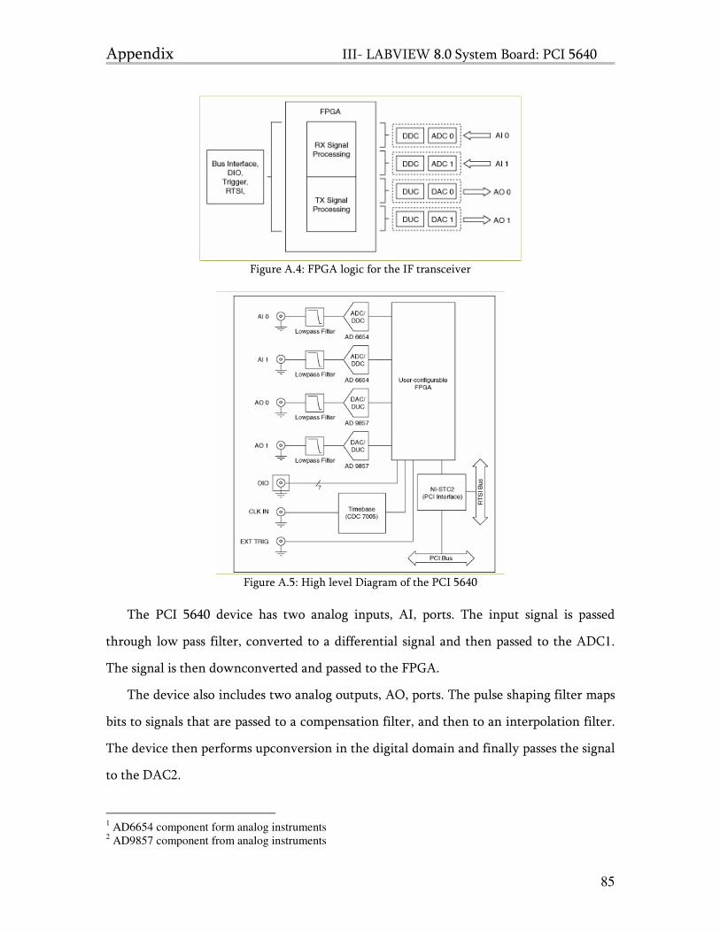
III-LABVIEW 8.0 System Board: PCI 5640
The PCI 5640 device, a LABVIEW 8.0 RIO system board, is mainly based on a
reconfigurable FPGA and some fixed I/O resources, i.e. an IF transceiver. Unlike
traditional IF digitizers where the functionality of the system is completely
predetermined, the FPGA allows the user to configure the behavior of various modules to
meet the system requirements. The FPGA is built around a reconfigurable architecture
where the user can define I/O resources or create new ones. Figure A.3 shows a high level
diagram of the reconfigurable architecture [28].
Figure A.3: High level FPGA_ I/O architecture
The I/O resources can either be outputs of the ADC and DAC, digital input lines,
digital output lines …. Software modules access the device through the BUS interface
while the FPGA provides logic need for the connectivity1 between the bus interface and
the I/O resources. Figure A.4 illustrates the FPGA logic for the IF transceiver [28].
Figure A.5 shows a high level diagram of the PCI 5640 device. Note that the DC power
control and the memory modules are hidden to simply the diagram [28].
1 Timing, triggering, processing, custom I/O
Appendix III- LABVIEW 8.0 System Board: PCI 5640
85
Figure A.4: FPGA logic for the IF transceiver
Figure A.5: High level Diagram of the PCI 5640
The PCI 5640 device has two analog inputs, AI, ports. The input signal is passed
through low pass filter, converted to a differential signal and then passed to the ADC1.
The signal is then downconverted and passed to the FPGA.
The device also includes two analog outputs, AO, ports. The pulse shaping filter maps
bits to signals that are passed to a compensation filter, and then to an interpolation filter.
The device then performs upconversion in the digital domain and finally passes the signal
to the DAC2.
1 AD6654 component form analog instruments
2 AD9857 component from analog instruments
Appendix III- LABVIEW 8.0 System Board: PCI 5640
86
The RTSI, real time system integration bus, allows multiple RIO PCI-5640 devices to
share the same trigger and events’ synchronization signals.
The PCI bus provides PCI bus interface for the PCI 5640 device with bus mastering
capabilities. The PCI bus allows to efficiently transfer data between the host PC and the
5640 device.
The PCI 5640 device also includes onboard memory of 2 MB (SRAM) inaddition to
the RAM available in the Virtex-II Pro (XC2VP30) FPGA. Section IV in the Appendix
gives more details about the capabilities of the FPGA.
The advantage of such board in our project is that it uses a relatively easy software,
LABVIEW, and thus hides the complexity of the common HDL languages, VHDL and
Verilog, that are commonly used to design hardware components. Moreover, it also
supports designs that are created using HDL. So, modules created using VHDL or some
other HDL language can be imported to the LABVIEW as custom VIs
Appendix IV- Virtex-II Pro FPGA Capabilities
87
IV- Virtex II Pro FPGA Capabilities
The LABVIEW 8.0 PCI 5640 System board contains a Virtex II Pro device that is
connected to all resources on the device (ADC, DAC, clk distribution circuit (CDC),
external trigger…). The Virtex II Pro is a platform FPGA based on IP cores and
customized modules [29]. The device present in our system board is the XC2VP30 FPGA.
This kind of device incorporates many resources and features some of which are:
----RocketIO transceiver blocks:RocketIO transceiver blocks:RocketIO transceiver blocks:RocketIO transceiver blocks: a full duplex serial transceiver whose baud rates range
from 600 Mbits/sec to 3.125 Gbits/sec. It is a flexible serial to parallel and parallel to serial
embedded transceiver cores used to interconnect busses, backplanes or other subsystems
with high bandwidth [29]. Our device supports up to 8 RocketIO transceiver blocks.
----PowerPC Processor blocksPowerPC Processor blocksPowerPC Processor blocksPowerPC Processor blocks: an embedded 300 MHz or more with Harvard architecture
block. It can execute instructions at a sustained rate of 1 instruction per cycle. Our
device can support up to 2 PowerPC processors [29].
----30816 logic cells30816 logic cells30816 logic cells30816 logic cells where a logic cell is defined as
----18x18 multiplier block18x18 multiplier block18x18 multiplier block18x18 multiplier block: an 18 bit x 18 bit multiplier block. The block is a two’s
complement signed multiplier and is characterized by a very efficient structure. The
device can hold up to 136 multiplier blocks.
----SelectRAM+ blockSelectRAM+ blockSelectRAM+ blockSelectRAM+ block: this block contains memory resources of 18 Kb of True Dual Port
RAM. It can be cascaded to implement large memory blocks. Our device supports 136
18Kb blocks with MaxBlock RAM of 2448 Kb.
----Max User I/O pads of 644Max User I/O pads of 644Max User I/O pads of 644Max User I/O pads of 644
----DCMDCMDCMDCM: digital clock manager; provides self calibrating, fully digital solutions for clock
distribution delay compensation, clock multiplication and division, and fine and coarse
clock phase shifting. Our device can support up to 8 DCMs.
Appendix V- Fixed Point Notation
88
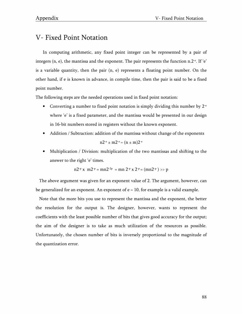
V- Fixed Point Notation
In computing arithmetic, any fixed point integer can be represented by a pair of
integers (n, e), the mantissa and the exponent. The pair represents the function n.2-e. If ‘e’
is a variable quantity, then the pair (n, e) represents a floating point number. On the
other hand, if e is known in advance, in compile time, then the pair is said to be a fixed
point number.
The following steps are the needed operations used in fixed point notation:
• Converting a number to fixed point notation is simply dividing this number by 2-e
where ‘e’ is a fixed parameter, and the mantissa would be presented in our design
in 16-bit numbers stored in registers without the known exponent.
• Addition / Subtraction: addition of the mantissa without change of the exponents
n2-e ± m2-e = (n ± m)2-e
• Multiplication / Division: multiplication of the two mantissas and shifting to the
answer to the right ‘e’ times.
n2-p x m2-p = mn2-2p = mn 2-p x 2-p = (mn2-p ) >> p
The above argument was given for an exponent value of 2. The argument, however, can
be generalized for an exponent. An exponent of e = 10, for example is a valid example.
Note that the more bits you use to represent the mantissa and the exponent, the better
the resolution for the output is. The designer, however, wants to represent the
coefficients with the least possible number of bits that gives good accuracy for the output;
the aim of the designer is to take as much utilization of the resources as possible.
Unfortunately, the chosen number of bits is inversely proportional to the magnitude of
the quantization error.
89
BibliographyBibliographyBibliographyBibliography
1. Buracchini, E. “The software radio concept”. IEEE, Communications Magazine.