Research and design of high precise adjustable power supply device
LIU Hong-bing (Hunan Railway Professional Technology College, Zhuzhou, 412001)
Keywords: LDO; Adjustable power supply; Voltage surge; Ripple;
Abstract. This paper research and design a precision adjustable power supply. Thevoltage in the range of 3.3V to 3.4V, the ripple voltage and its peak value of not more than 100mV, power is about 1W, the power supply can be provided to theoptical module, its security is good, and can support the RF device,the power supply starting surge voltage time close to 0. In the choice of method of removing surge ripple, designed a rated output voltage 5V, rated output current of 1A low dropout linear regulator (LDO), the device is compared to the DC/DC circuit, effectively reducing the ripple. By experimental verification, the design scheme is feasible, and has good application value.
Introduction
With the rapid development of information science technology, power supply becomes more and more important. Especially low voltage stabilized power supply more popular in intelligent instruments and today, more and more extensive application, low voltage stabilizing circuit so the research and design of adjustable power supply technology, become the focus again in the. In recent years, with the development and application of sensor technology, optical module is used more and more in the sensor circuit, driving the light module of the power supply requirements of high stability, and the price is expensive, the voltage fluctuation exceeds a certain range, it is easy to burn【1,2,3】,Therefore, in this paper a technique parameters in the drive voltage of between 3.3V-3.4V,optical module and ripple peak voltage should not exceed 100mV, the design of adjustable power supply, a high precision. The ripple power to remove the circuit using LDO, which has a small volume, high power supply rejection ratio, low power consumption, low noise and the advantages of simple circuit application end, in addition, LDO also has a good linear transient response and load transient response, complete the design of the high precision adjustable power supply can provide light module in 25GHz, security is good, can support the RF device, and the power supply startup surge voltage close to 0.
The design of LDO device
LDO consists of a current source, voltage reference, error amplifier, adjust the tube and a sampling circuit, the design of the power performance requirements of rated voltage 5V, output current 1A; power measurement module circuit signals are input to collection points magnification, A/D conversion module and then input to the STC12C5A60S2 SCM, the analog signal is converted to digital signal [6], and then through the single-chip power calculation, through the liquid crystal display power; leakage protection module input the signal acquisition to the amplifier circuit, signal amplification, two ways of signal amplification signal output by control RS trigger is more amplified, control relay drive circuit, the realization of leakage protection and automatic cutting. The schematic diagram shown in Fig. 1.
International Conference on Applied Science and Engineering Innovation (ASEI 2015)
The power from the constant current source (the core components for the PNP pipe, NPN pipe, Q1 voltage reference (Q2) voltage regulator tube, an error amplifier (D1) integrated operational amplifier (OP295), adjusting pipe (two PNP tubes Q4 and Q5) and a sampling circuit, reached the rated voltage 5V, output current performance requirements 1A. The sampling voltage is applied on the in-phase input terminal of the comparator OP295, compared with the added to the inverting input terminal of the reference voltage Uz , the difference between the two after the amplifier amplified OP295series adjustment, control pipe pressure drop, and thus the stability of the output voltage. When the output voltage of Uout is reduced, the difference between the reference voltage and a sample voltage increases, the comparison amplifier output driving current increase, series adjusting pipe pressure drop decreases, so that the output voltage rise. On the contrary, if the output voltage exceeds the set value of Uout required, comparison amplifier out put front drive current is reduced, thereby reducing the output voltage. The specific circuit as shown in Fig 2.
Fig. 2 LDO unit circuit
The design of the adjustable voltage unit circuit
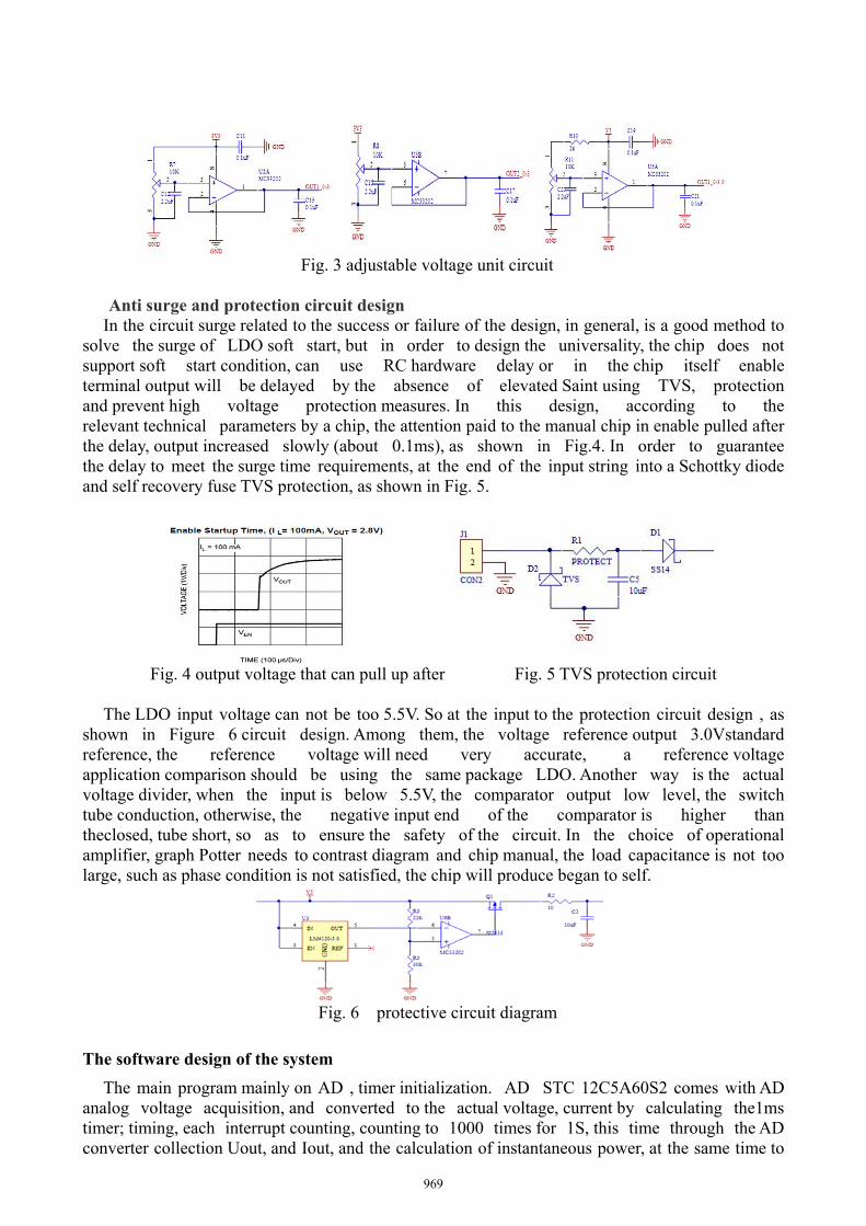
Fig. 3 is the adjustable voltage unit circuit, are the input and output of rail2rail, so as to ensure maximum adjustable range. One way is to be transferred to the 5V, so that the sliding way and a resistor string, to ensure that such plus electrical output in 5v5 is also less than 5V, because generally lowered the rarely used 5V voltage, so the voltage lower than 5V has little.
968
Fig. 3 adjustable voltage unit circuit
Anti surge and protection circuit design In the circuit surge related to the success or failure of the design, in general, is a good method to
solve the surge of LDO soft start, but in order to design the universality, the chip does not support soft start condition, can use RC hardware delay or in the chip itself enable terminal output will be delayed by the absence of elevated Saint using TVS, protection and prevent high voltage protection measures. In this design, according to the relevant technical parameters by a chip, the attention paid to the manual chip in enable pulled after the delay, output increased slowly (about 0.1ms), as shown in Fig.4. In order to guarantee the delay to meet the surge time requirements, at the end of the input string into a Schottky diode and self recovery fuse TVS protection, as shown in Fig. 5.
Fig. 4 output voltage that can pull up after Fig. 5 TVS protection circuit
The LDO input voltage can not be too 5.5V. So at the input to the protection circuit design , as
shown in Figure 6 circuit design. Among them, the voltage reference output 3.0Vstandard reference, the reference voltage will need very accurate, a reference voltage application comparison should be using the same package LDO. Another way is the actual voltage divider, when the input is below 5.5V, the comparator output low level, the switch tube conduction, otherwise, the negative input end of the comparator is higher than theclosed, tube short, so as to ensure the safety of the circuit. In the choice of operational amplifier, graph Potter needs to contrast diagram and chip manual, the load capacitance is not too large, such as phase condition is not satisfied, the chip will produce began to self.
Fig. 6 protective circuit diagram
The software design of the system
The main program mainly on AD , timer initialization. AD STC 12C5A60S2 comes with AD analog voltage acquisition, and converted to the actual voltage, current by calculating the1ms timer; timing, each interrupt counting, counting to 1000 times for 1S, this time through the AD converter collection Uout, and Iout, and the calculation of instantaneous power, at the same time to
969
send LCD display. Data acquisition frequency is 1HZ. The program flow chart as shown in Fig. 7.
Start
( )Interrupt initialization T0
LCD initialization
AD initialization
Wait
The stop start
The initial value of timer
A second time?
Acquisition of U and I, the calculation of P
Display
Interrupt return
N
Y
The flow chart of the main program T0 timer interrupt subroutine flow chart
Fig. 7 system program flow chart
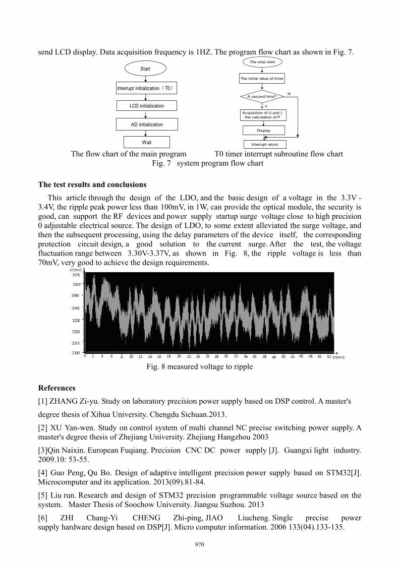
The test results and conclusions
This article through the design of the LDO, and the basic design of a voltage in the 3.3V - 3.4V, the ripple peak power less than 100mV, in 1W, can provide the optical module, the security is good, can support the RF devices and power supply startup surge voltage close to high precision 0 adjustable electrical source. The design of LDO, to some extent alleviated the surge voltage, and then the subsequent processing, using the delay parameters of the device itself, the corresponding protection circuit design, a good solution to the current surge. After the test, the voltage fluctuation range between 3.30V-3.37V, as shown in Fig. 8, the ripple voltage is less than 70mV, very good to achieve the design requirements.
Fig. 8 measured voltage to ripple
References
[1] ZHANG Zi-yu. Study on laboratory precision power supply based on DSP control. A master's
degree thesis of Xihua University. Chengdu Sichuan.2013.
[2] XU Yan-wen. Study on control system of multi channel NC precise switching power supply. A master's degree thesis of Zhejiang University. Zhejiang Hangzhou 2003
[3]Qin Naixin. European Fuqiang. Precision CNC DC power supply [J]. Guangxi light industry. 2009.10: 53-55.
[4] Guo Peng, Qu Bo. Design of adaptive intelligent precision power supply based on STM32[J]. Microcomputer and its application. 2013(09).81-84.
[5] Liu run. Research and design of STM32 precision programmable voltage source based on the system. Master Thesis of Soochow University. Jiangsu Suzhou. 2013
[6] ZHI Chang-Yi CHENG Zhi-ping, JIAO Liucheng. Single precise power supply hardware design based on DSP[J]. Micro computer information. 2006 133(04).133-135.
970
[7] SU Lei, LIE bin, Mao Xiu-fen. Design and implementation of a thermal conductivity detector precision constant current source [J]. Microcomputer and its application. 2011.14(30),16-19.