Shanghai Institute of Microsystem and Information Technology Research progress of SOI devices and modeling in SIMIT State Key Laboratory of Functional Materials for Informatics Shanghai Institute of Microsystem and Information Technology Chinese Academy of Sciences Jun. 27, 2016 Jing Chen 1 Email: [email protected]
Transcript
Shanghai Institute of Microsystem and Information Technology
Research progress of SOI devices and modeling in SIMIT
State Key Laboratory of Functional Materials for InformaticsShanghai Institute of Microsystem and Information Technology
Shanghai Institute of Microsystem and Information Technology
Outline
Introduction of SOI Group
Research results
Summary
DC Device Model
RF Device Model
Research of SOI Device
Fruits of international cooperation
2
Shanghai Institute of Microsystem and Information Technology
Staff
3
Prof. Xi Wang Academician of the Chinese Academy of
Sciences
Prof. Shichang ZouAcademician of the Chinese Academy of
Sciences
Total 78 people 14 professors 10 associate Professors 38 graduate students
Shanghai Institute of Microsystem and Information Technology 4
Research field
• SiGe, Strain SOI• GaN, GrapheneSOI Material
• Process, Device, Modeling• PDK, Library, IP
SOI Design Service
• ASIC, FPGA, ADC, SwitchSOI Circuit
• AWG, MMI, High-end microprocessorSOI Photonics
SIMIT research teams are actively driving new SOI technologydevelopment, e.g. material, device, process, design services,products etc., help to build up SOI ecosystem.
Shanghai Institute of Microsystem and Information Technology 5
100+ papers published, 150+ patents applied ( including 50+ international), within the last 5 years.
the Prize of National Science & Technology Advancement (1st grade)
Achievements
Shanghai Institute of Microsystem and Information Technology 6
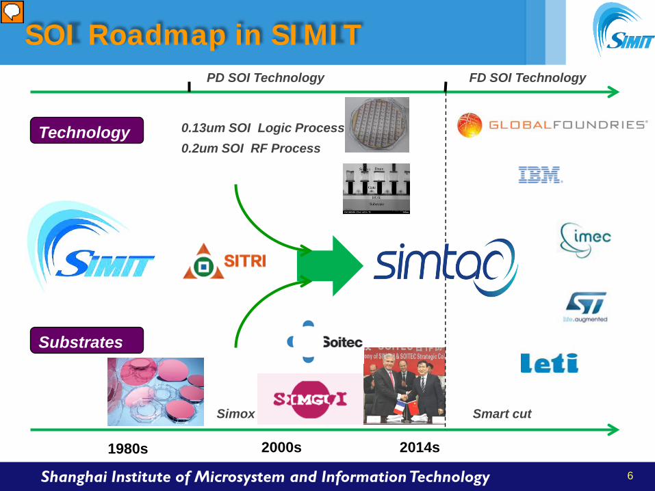
SOI Roadmap in SIMIT
Simox Smart cut
0.13um SOI Logic Process0.2um SOI RF Process
Technology
PD SOI Technology FD SOI Technology
Substrates
1980s 2000s 2014s
演示者
演示文稿备注
Through the SIMTAC platform, we will establish a more close cooperation with industry, and promoting the transformation of SOI research results.
Shanghai Institute of Microsystem and Information Technology 7
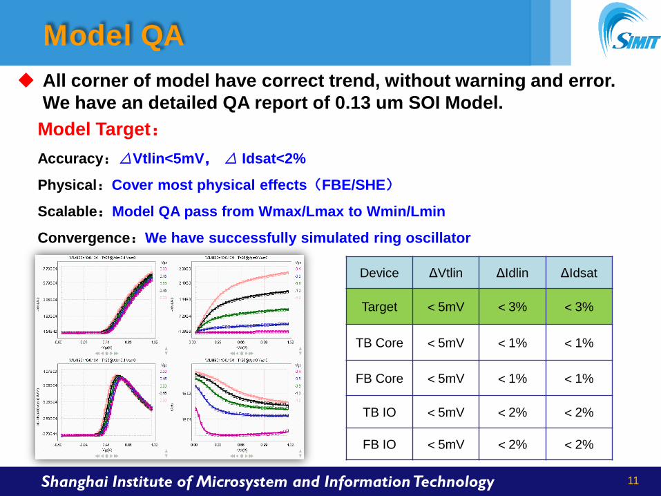
• TT, FF, SS, FS, SFCornerSimulation result of RF NMOS
Shanghai Institute of Microsystem and Information Technology 16
0.13 um SOI model was applied to SOI Library and ASIC circuit design. The model has become an important part of 0.13 um SOI technology
platform, which provides a powerful guarantee for the SOI highreliability circuit design.
Chip Parameters Performance
Working Frequency 50Mhz
Chip Scale > 2M gates
Chip Area 8mm x 9mm
Dynamic Power 250mA
ASIC Chip Verification
Application of SOI Model
Shanghai Institute of Microsystem and Information Technology 17
Novel Body Contact Structure
0.0 0.3 0.6 0.9 1.20
1
2
3
4
5
6
W/L=10um/0.13um
FB SOI TDBC SOI
PD SOI nMOSFET@VG=0.6~1.2V, Step=0.2V
Drai
n Cu
rrent
, I D(m
A)
Drain Voltage, VD (V)
•Jing Chen, Jiexin Luo et al., IEEE Electron Device Letters, 32(10), 1346, 2011•Jiexin Luo, Jing Chen et al., IEEE Transactions on Electron Devices, 59(1), 101, 2012•Kai Lu, Jing Chen et al., IEEE Electron Device Letters, 35(1), 15, 2014
-0.2 0.0 0.2 0.4 0.6 0.8 1.00
10
20
30
40
50
60
70
80
90
100
-0.2 0.0 0.2 0.4 0.6 0.8 1.0102030405060708090
100110120130140
f T(G
Hz)
VGS-VTH(V)
FB TB TDBC
(a) (b)
f MAX
(GH
z)
VGS-VTH(V)
FB TB TDBC
TDBC SOI devices without floating-body effects are successfullydemonstrated, which represent an improvement of 10% for the fTand of 90% for the fMAX compared with conventional T-gate body-contact devices.
Kink are perfectly suppressed in TDBC devices Superior RF performance of TDBC devices
Shanghai Institute of Microsystem and Information Technology 18
TDBC contact makes these SOI transistors strongly resistant to back channel radiation effects.
Jiexin Luo, Jing Chen et al., IEEE Transaction on Nuclear Science, 61(6), 11, 2014
It is expected to find applications in designing compact opticalcomponents to achieve the on-chip beam steering in photonic circuits.
Shanghai Institute of Microsystem and Information Technology 22
High-K SiGe/SOI quantum well
•Bo Zhang et al., Applied Physics Letters, 98, 252101 (2011)•Bo Zhang et al., Solid-State Electronics, 62(1), 185, 2011
sSi/sSiGe/sSOI substrate 2.5X larger than Bulk channelCarries are confined in sSiGe
Hol
e m
obili
ty
Cooperated with Juelich Research Center, Germany
Epitaxial growth of strain silicon substrates was achieved via an Alinterlayer mediated epitaxial. The hole mobility is 2.5X larger thanBulk channel.
Shanghai Institute of Microsystem and Information Technology 23
Nanowire on SOI
•Xin Ou et al., Nano Letters, 10(1), 171, 2010
Perfect structure with gate all-rounded
Easy to implement on SOI
Nanowire on Hybrid orientation SOI
100 nm
SSRM (Scanning Spreading Resistance Microscopy)
Cooperated with ForschungszentrumDresden-Rossendorf, Germany
•Xin Ou et al., Advanced Materials, 22(36), 4020, 2010
•Xiao Deyuan et al., Journal of Semiconductors, 30(1), 2009
SSRM has been used to characterize doping in silicon nanowire for the firsttime. The GAAC FinFET appears to be a good potential candidate forscaling down to sub-10 nm sizes.
Shanghai Institute of Microsystem and Information Technology
Outline
Introduction of SOI Group
Research results
Summary
24
DC Device Model
RF Device Model
Research of SOI Device
Fruits of international cooperation
Shanghai Institute of Microsystem and Information Technology 25
Summary
• The leading SOI research teams in China areactively driving new SOI technologydevelopment, help to build up SOI ecosystem.
SOI Group
• We have extracted a complete Model for 0.13um SOI technology, which was applied to SOILibrary and ASIC circuit design.
Device Modeling
• We have designed TDBC SOI device, FBGC Cell,LDMOS, Nanowire, Silicon photonics integratedchip, and so on.
Research of SOI Device
• We have fruits of international cooperation with some famous university in USA and Research Centers in Germany.
International cooperation
Shanghai Institute of Microsystem and Information Technology