25
International RF-SOI Workshop Shanghai, September 2017 Leveraging SOI in RFIC Analog Subsystems Yoshiharu Furui

International RF-SOI Workshop
Shanghai, September 2017
Leveraging SOI in RFIC Analog Subsystems
Yoshiharu Furui

• Introduction to Silvaco
• Real-world example of leveraging FD-SOI in RFIC
• Design flow and tool considerations
• Conclusion
Agenda
- 2 -

• Leading TCAD, EDA and IP provider
• Founded in 1984
• Worldwide footprint of 400+ customers
• 200 employees with global footprint in United States, United Kingdom,
France, Japan, Korea, Taiwan, China, Singapore, India
• Delivering complete TCAD-to-Signoff product portfolio
• TCAD, 3D RC extraction
• SPICE modeling & simulation, Variation Analysis
• Custom IC Design and Power Integrity Signoff
• Growth vision to ensure long term strength for Silvaco’s customers
Silvaco Introduction
- 3 -
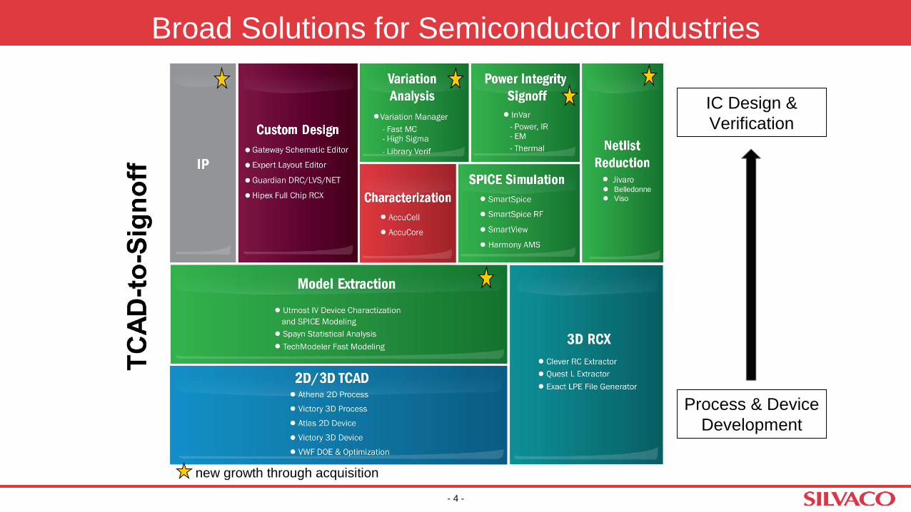
Process & Device
Development
IC Design &
Verification
Broad Solutions for Semiconductor Industries
Belledonne
Viso
new growth through acquisition
- 4 -
Silvaco Confidential
Real-world example of leveraging FD-SOI in RFIC
- 5 -

Typical RFIC System
Radio divided into 2 sections, RF and Baseband
• RF 700Mhz to 3.5Ghz (LTE), 2.4Ghz/5Ghz (WiFi)
• Baseband <100Mhz operation (low Frequency)
Duplexer
RFout
(TX)
RFin
(RX)
RF
in/out
- 6 -

Product Example from Partner: Seamless Devices
High SNDR at low power and small area
Half the power of best-in-class ADCs with
better SNDR
Bandwidth SNDR Power Clock Jitter SFDR Supply Technology
SD40M Measured
40MHz 68.4dB 25.3mW
4ps rms 82dB
0.9V 28nm Simulated 70dB 24.8mW -
SD80M Measured
80MHz 65dB 41.7mW
2ps rms 81dB
0.9V 28nm Simulated 68dB 37mW -
Low overall system cost
Single core voltage supply operation
Robust jitter-tolerant design (up to 4ps)
Easy to integrate IP block • No need for complex anti-aliasing block
• Resistive input is easier to drive
• Highly integrated solution
DECAP
DECAP
BANDGAP
DEC
APSD40M
DECAP
DECAP
BANDGAP
DEC
APSD80M
Si-proven Si-proven
- 7 -
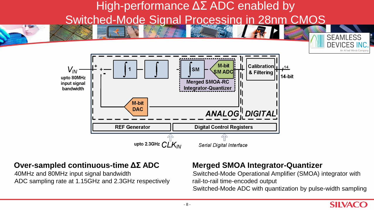
High-performance ΔΣ ADC enabled by
Switched-Mode Signal Processing in 28nm CMOS
Over-sampled continuous-time ΔΣ ADC •40MHz and 80MHz input signal bandwidth
•ADC sampling rate at 1.15GHz and 2.3GHz respectively
Merged SMOA Integrator-Quantizer •Switched-Mode Operational Amplifier (SMOA) integrator with
rail-to-rail time-encoded output
•Switched-Mode ADC with quantization by pulse-width sampling
- 8 -
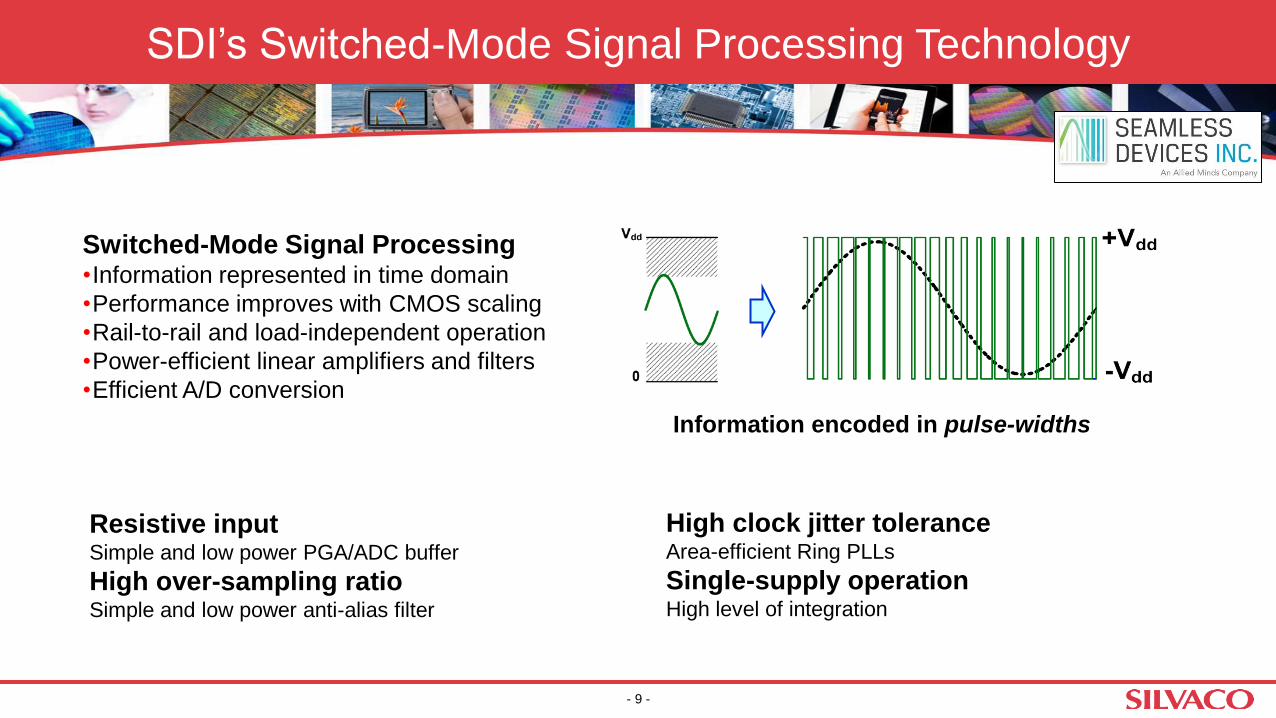
SDI’s Switched-Mode Signal Processing Technology
Switched-Mode Signal Processing •Information represented in time domain
•Performance improves with CMOS scaling
•Rail-to-rail and load-independent operation
•Power-efficient linear amplifiers and filters
•Efficient A/D conversion
Information encoded in pulse-widths
High clock jitter tolerance Area-efficient Ring PLLs
Single-supply operation High level of integration
Resistive input Simple and low power PGA/ADC buffer
High over-sampling ratio Simple and low power anti-alias filter
- 9 -
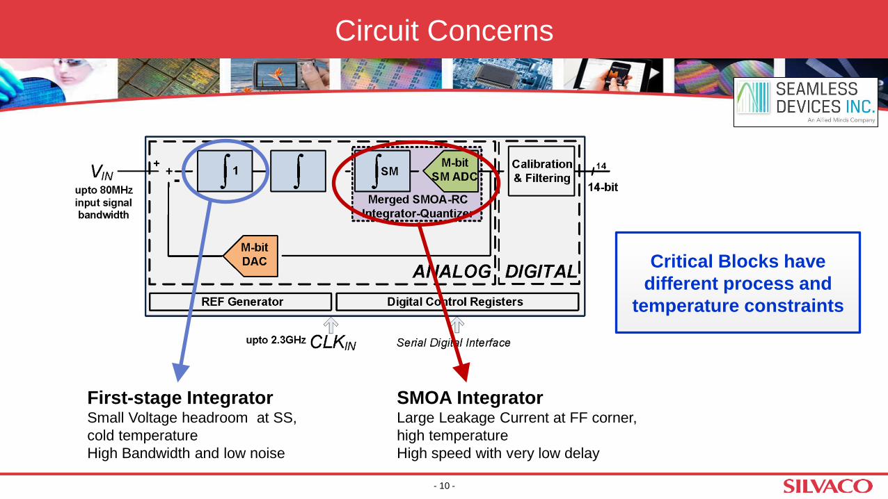
Circuit Concerns
First-stage Integrator Small Voltage headroom at SS,
cold temperature
High Bandwidth and low noise
SMOA Integrator Large Leakage Current at FF corner,
high temperature
High speed with very low delay
Critical Blocks have
different process and
temperature constraints
- 10 -

•Problem: Low voltage headroom at SS corner •Available voltage headroom is 50-80mV at SS corner, cold temperature, low VDD,
•results in Larger devices sizes => Large capacitance => Lower bandwidth and higher power consumption
First Stage Integrator Design Challenges
•Solution: using FD-SOI •Larger voltage headroom at SS, low temp, low VDD
•using forward body biasing
•- Gains about 100mV-150mV of headroom
•- Smaller devices sizes enables higher bandwidth and
• lower power consumption
•=> 20% Power reduction in FD-SOI
- 11 -

•Problem: SMOA requires low delay operation for stability considerations •Low Vt transistors are required for low delay in SS, low temp., low VDD
•Low Vt transistor have significant leakage in FF, high temp., high VDD
SMOA Integrator Design Challenges
•Solution: using FD-SOI •Adaptive body bias for corners vs speed/leakage trade-off
- at SS, low temp., low VDD
• Higher body bias to reduce delay
•- at FF, high temp., high VDD
• Lower body bias to reduce leakage
•=> 50% Power reduction in FD-SOI
- 12 -

Silvaco Confidential
Design flow and tool considerations
- 13 -
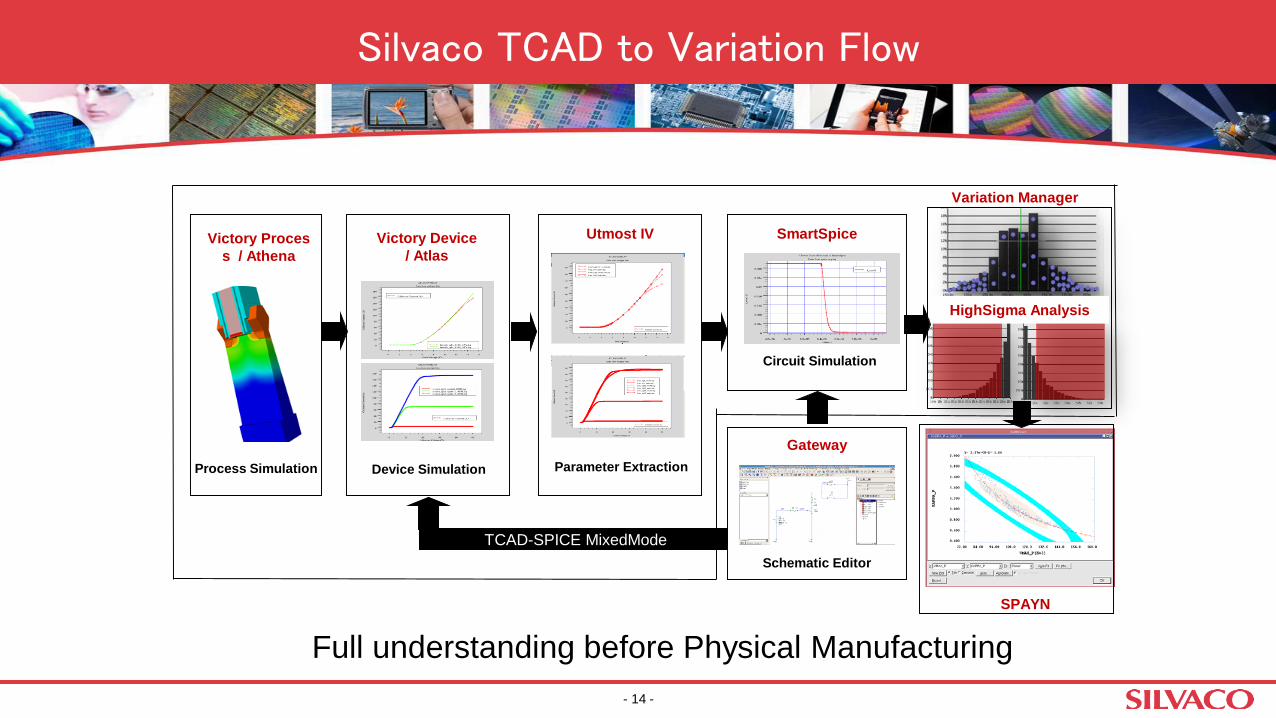
Silvaco TCAD to Variation Flow
Victory Proces
s / Athena
Victory Device
/ Atlas
Utmost IV SmartSpice
Circuit Simulation
Parameter Extraction Device Simulation Process Simulation
Gateway
Schematic Editor
TCAD-SPICE MixedMode
SPAYN
Variation Manager
HighSigma Analysis
Full understanding before Physical Manufacturing
- 14 -
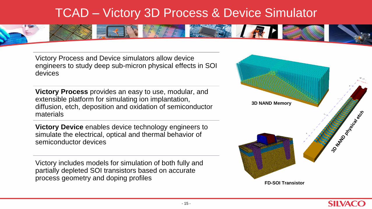
TCAD – Victory 3D Process & Device Simulator
3D NAND Memory
Victory Process and Device simulators allow device engineers to study deep sub-micron physical effects in SOI devices
Victory includes models for simulation of both fully and partially depleted SOI transistors based on accurate process geometry and doping profiles
Victory Process provides an easy to use, modular, and extensible platform for simulating ion implantation, diffusion, etch, deposition and oxidation of semiconductor materials Victory Device enables device technology engineers to simulate the electrical, optical and thermal behavior of semiconductor devices
- 15 -
FD-SOI Transistor

Fully Depleted. Effect of Body Bias
20nm FD-SOI simulated by Victory
Reverse Body Bias increases Vth but decreases leakage,
Forward Body Bias increases Leakage but decreases Vth (making device faster)
- 16 -
FBB
RBB
No Body Bias
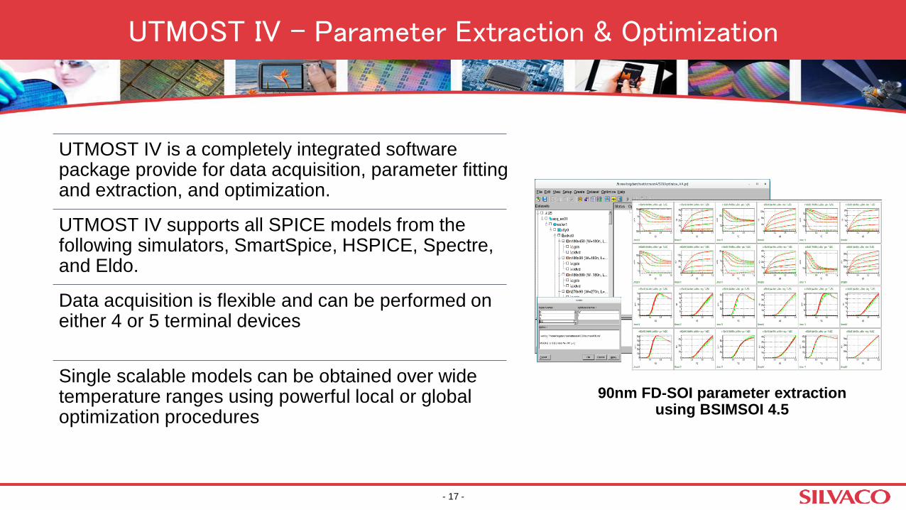
UTMOST IV is a completely integrated software package provide for data acquisition, parameter fitting and extraction, and optimization.
UTMOST IV supports all SPICE models from the following simulators, SmartSpice, HSPICE, Spectre, and Eldo.
Data acquisition is flexible and can be performed on either 4 or 5 terminal devices
Single scalable models can be obtained over wide temperature ranges using powerful local or global optimization procedures
UTMOST IV - Parameter Extraction & Optimization
90nm FD-SOI parameter extraction using BSIMSOI 4.5
- 17 -

Supported SOI Compact Models in Silvaco Tools
PDSOI FDSOI UTBB-FDSOI
BSIM-SOI v3.0-3.2 and v4.0-4.5
BSIM-IMG v102.0-102.8
HiSIM-SOI v1.0.0-v1.3.0
HiSIM-SOTB v1.0.0-1.1.0
LETI-SOI v3.0-3.2 v4.0
LETI-UTSOI v2.1
- 18 -
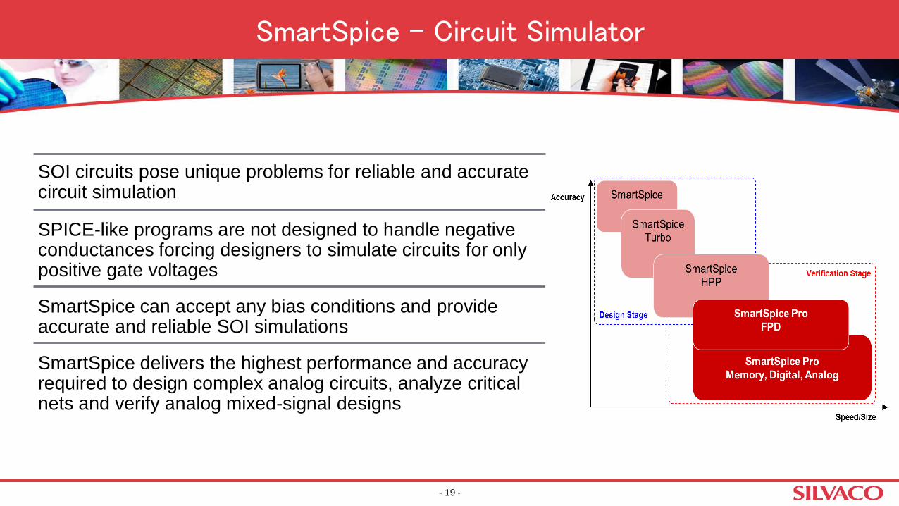
SOI circuits pose unique problems for reliable and accurate circuit simulation
SPICE-like programs are not designed to handle negative conductances forcing designers to simulate circuits for only positive gate voltages
SmartSpice can accept any bias conditions and provide accurate and reliable SOI simulations
SmartSpice delivers the highest performance and accuracy required to design complex analog circuits, analyze critical nets and verify analog mixed-signal designs
SmartSpice - Circuit Simulator
- 19 -

Power Integrity and Reliability Analysis
InVar Power InVar IR InVar EM
InVar Thermal
Concurrent Power-Voltage-Thermal Analysis Block to full chip level
Quick design analysis to signoff
Early (layout only) IR/EM analysis
TSMC N16FF+ certified for Gate level
Pure SPICE accuracy for Transistor level
- 20 -

Variation Analysis
Sense Amplifier, FD-SOI 28nm
Variation Manager validated on 1M of MC runs
Q-Q Plot (sigma vs performance) Brute Force MC vs Variation Manager
Red: Monte Carlo (1M runs)
Blue: Variation Manager (2K runs) Extremes
- 21 -
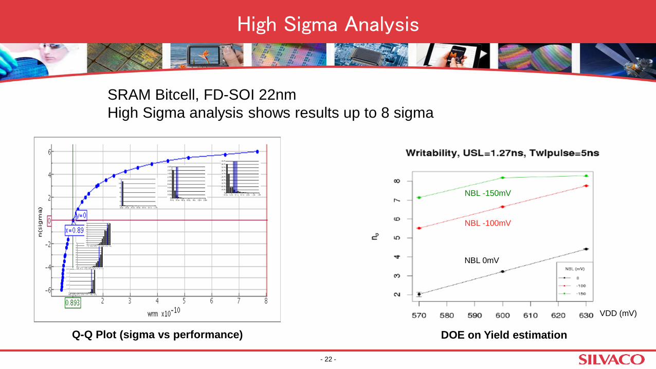
High Sigma Analysis
Q-Q Plot (sigma vs performance) DOE on Yield estimation
VDD (mV)
NBL 0mV
NBL -100mV
NBL -150mV
SRAM Bitcell, FD-SOI 22nm
High Sigma analysis shows results up to 8 sigma
- 22 -
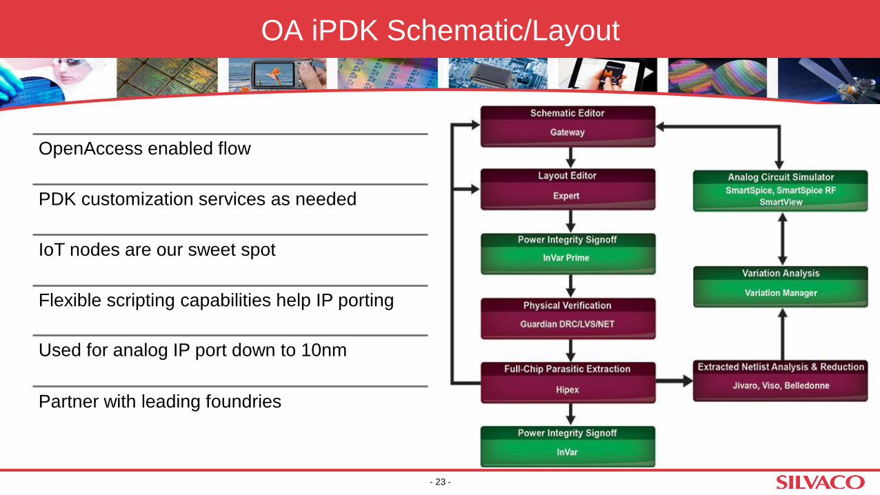
OA iPDK Schematic/Layout
OpenAccess enabled flow
PDK customization services as needed
IoT nodes are our sweet spot
Flexible scripting capabilities help IP porting
Used for analog IP port down to 10nm
Partner with leading foundries
- 23 -

Silvaco IP Businesses
• Collaborations with Tier 1 semiconductor companies to unlock valuable IP for licensing to the entire semiconductor industry
IP Commercialization
• Powered by Silvaco’s Xena IP Management Software an on-line catalog for IP Vendors to offer their IP Solutions to customers.
On-Line IP Store
• Xena is a scalable cloud-based platform for managing IP inside semiconductor and IP companies
IP Management
• IP Fingerprinting and DNA analysis that allows for detection of IP in SoC devices
IP Compliance
- 24 -

• Global EDA Leader driving growth to provide value to our customers in
Advanced IC, Display, Power and AMS
• Provider delivering complete TCAD-to-Signoff solutions for predictive and
comprehensive design work before applying $$$ to Silicon
• Utilizing acquisitions combined with organic development to drive high
growth rate
• Custom CAD supports fabless community across many foundries
• New IP division with unique IP Fingerprint tools allow Silvaco to participate
in the highest growth area of EDA
• Financially strong driving double digit growth from the balance sheet
• Cost Effective partner to the FD-SOI community
Conclusion
- 25 -


