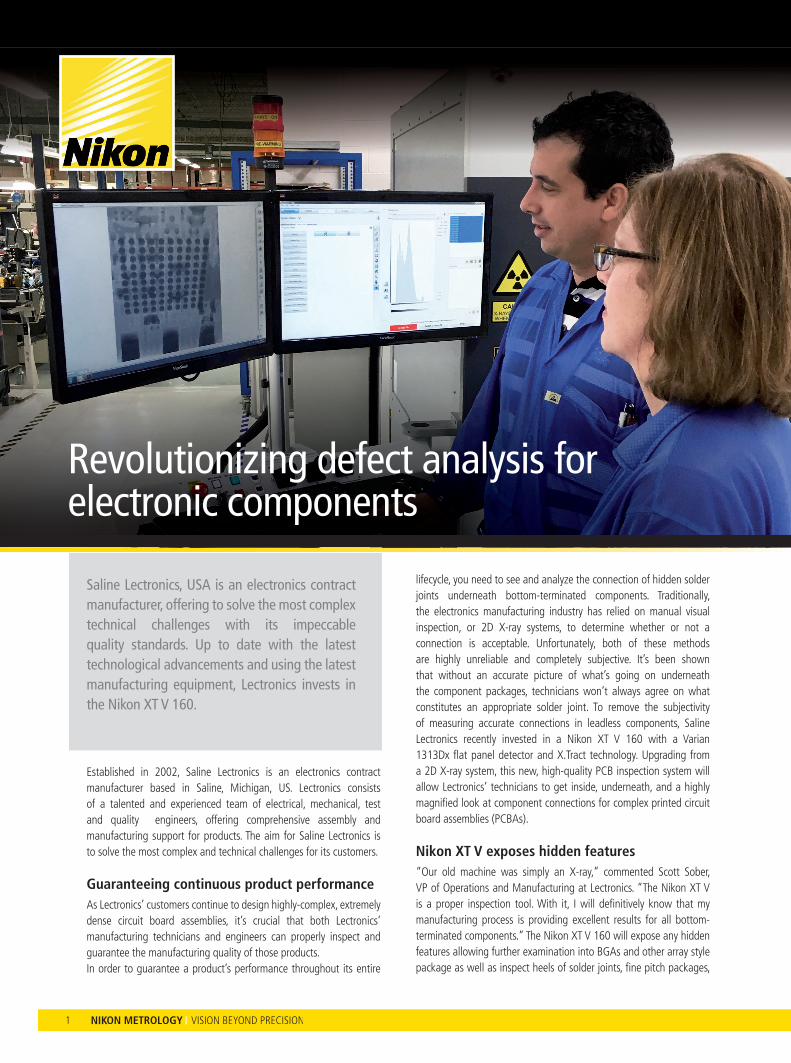
lifecycle, you need to see and analyze the connection of hidden solder joints underneath bottom-terminated components. Traditionally, the electronics manufacturing industry has relied on manual visual inspection, or 2D X-ray systems, to determine whether or not a connection is acceptable. Unfortunately, both of these methods are highly unreliable and completely subjective. It’s been shown that without an accurate picture of what’s going on underneath the component packages, technicians won’t always agree on what constitutes an appropriate solder joint. To remove the subjectivity of measuring accurate connections in leadless components, Saline Lectronics recently invested in a Nikon XT V 160 with a Varian 1313Dx flat panel detector and X.Tract technology. Upgrading from a 2D X-ray system, this new, high-quality PCB inspection system will allow Lectronics’ technicians to get inside, underneath, and a highly magnified look at component connections for complex printed circuit board assemblies (PCBAs). Nikon XT V exposes hidden features “Our old machine was simply an X-ray,” commented Scott Sober, VP of Operations and Manufacturing at Lectronics. “The Nikon XT V is a proper inspection tool. With it, I will definitively know that my manufacturing process is providing excellent results for all bottom- terminated components.” The Nikon XT V 160 will expose any hidden features allowing further examination into BGAs and other array style package as well as inspect heels of solder joints, fine pitch packages, Saline Lectronics, USA is an electronics contract manufacturer, offering to solve the most complex technical challenges with its impeccable quality standards. Up to date with the latest technological advancements and using the latest manufacturing equipment, Lectronics invests in the Nikon XT V 160. 1 Revolutionizing defect analysis for electronic components Established in 2002, Saline Lectronics is an electronics contract manufacturer based in Saline, Michigan, US. Lectronics consists of a talented and experienced team of electrical, mechanical, test and quality engineers, offering comprehensive assembly and manufacturing support for products. The aim for Saline Lectronics is to solve the most complex and technical challenges for its customers. Guaranteeing continuous product performance As Lectronics’ customers continue to design highly-complex, extremely dense circuit board assemblies, it’s crucial that both Lectronics’ manufacturing technicians and engineers can properly inspect and guarantee the manufacturing quality of those products. In order to guarantee a product’s performance throughout its entire
Transcript
lifecycle, you need to see and analyze the connection of hidden solder joints underneath bottom-terminated components. Traditionally, the electronics manufacturing industry has relied on manual visual inspection, or 2D X-ray systems, to determine whether or not a connection is acceptable. Unfortunately, both of these methods are highly unreliable and completely subjective. It’s been shown that without an accurate picture of what’s going on underneath the component packages, technicians won’t always agree on what constitutes an appropriate solder joint. To remove the subjectivity of measuring accurate connections in leadless components, Saline Lectronics recently invested in a Nikon XT V 160 with a Varian 1313Dx fl at panel detector and X.Tract technology. Upgrading from a 2D X-ray system, this new, high-quality PCB inspection system will allow Lectronics’ technicians to get inside, underneath, and a highly magnifi ed look at component connections for complex printed circuit board assemblies (PCBAs).
Nikon XT V exposes hidden features“Our old machine was simply an X-ray,” commented Scott Sober, VP of Operations and Manufacturing at Lectronics. “The Nikon XT V is a proper inspection tool. With it, I will defi nitively know that my manufacturing process is providing excellent results for all bottom-terminated components.” The Nikon XT V 160 will expose any hidden features allowing further examination into BGAs and other array style package as well as inspect heels of solder joints, fi ne pitch packages,
Saline Lectronics, USA is an electronics contract manufacturer, offering to solve the most complex technical challenges with its impeccable quality standards. Up to date with the latest technological advancements and using the latest manufacturing equipment, Lectronics invests in the Nikon XT V 160.
1
Revolutionizing defect analysis for electronic components
Established in 2002, Saline Lectronics is an electronics contract manufacturer based in Saline, Michigan, US. Lectronics consists of a talented and experienced team of electrical, mechanical, test and quality engineers, offering comprehensive assembly and manufacturing support for products. The aim for Saline Lectronics is to solve the most complex and technical challenges for its customers.
Guaranteeing continuous product performanceAs Lectronics’ customers continue to design highly-complex, extremely dense circuit board assemblies, it’s crucial that both Lectronics’ manufacturing technicians and engineers can properly inspect and guarantee the manufacturing quality of those products. In order to guarantee a product’s performance throughout its entire
and internal characteristics of solder joints. With a proprietary NanoTech 160kV X-ray spot and electromagnetic lens, this system offers the latest digital imaging technology available and produces clear, sharp images at the micron level.
This Nikon XT V 160 will also serve as an excellent process development tool for Lectronics. Getting clear pictures of specifi c areas on a PCBA that were not previously seen on Lectronics’ older X-ray, will help to reveal any hidden, unknown defects. With defects being brought to light sooner in the assembly process, Lectronics’ manufacturing team will be able to engage in root-cause analysis, and update production procedures in order to prevent the defects from re-occurring.
Automated X-ray inspection helps to save timeWith the automated inspection mode feature on the Nikon XT V 160, Lectronics will be able to program a variety of “routines” into the system that will function as batch Automated X-ray Inspection (AXI). These routines will automatically inspect a certain PCBA, or area of components on the PCB, and perform a full 2D and 3D analysis of the region of interest. This will enable Lectronics’ technicians to quickly and intuitively run routines of repeated inspections for production circuit board assemblies. Running routines will help Lectronics’ team save time on fi rst time build assemblies as well as during the troubleshooting process of any production fall-out. The Intelligent Program Control feature on the X-ray allows for customizable system control, which makes setting up the camera for each PCBA seamless and quick.
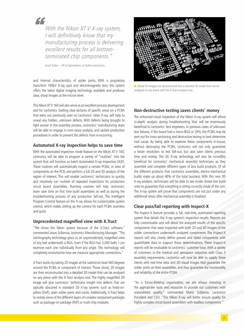
Unprecedented magnifi ed view with X.Tract“We chose the Nikon system because of the X.Tract software,” commented Jason Sciberras, Lectronics Manufacturing Manager. “The laminography technology gives us an unprecedented, magnifi ed view of any ball underneath a BGA. Even if the BGA has 2,000 balls, I can examine each one individually from any angle. This technology will completely revolutionize how we measure appropriate connections.”
X.Tract works by taking 2D images at the submicron level 360 degreesaround the PCBA or component of interest. Those sliced, 2D imagesare then reconstructed into a detailed 3D model that can be analyzedon any plane with the X.Tract analysis tool. The highly magnifi ed 3Dimage will give Lectronics’ technicians insight into defects that aretypically obscured in standard 2D X-ray systems such as head-on-pillow (HoP), open solder joints and cracks. Additionally, X.Tract helpsto isolate views of the different layers of complex component packages such as package-on-package (PoP) or multi-chip modules.
Non-destructive testing saves clients’ moneyThe enhanced visual inspection of the Nikon X-ray system will afford in-depth analysis during troubleshooting that will be enormously benefi cial to Lectronics’ test engineers. In previous cases of unknown test failures, if the board had a micro-BGA or QFN, the PCBA may be sent out for cross-sectioning and destructive testing to best determine root cause. By being able to examine these components in-house, without destroying the PCBA, Lectronics will not only guarantee a faster resolution to test fall-out, but also save clients precious time and money. The 3D X-ray technology will also be incredibly benefi cial for Lectronics’ mechanical assembly technicians as they assemble and complete different types of box build products. Of all the different products that Lectronics assembles, electro-mechanical builds make up about 40% of the total business. With this new 3D X-ray analysis, technicians will be able to see inside closed box buildunits to guarantee that everything is sitting correctly inside of the unit. The X-ray system will prove that components are not put under anyadditional stress after mechanical assembly is fi nalized.
Clear pass/fail reporting with Inspect-XThe Inspect-X feature provides a full, real-time, automated reporting system that details the X-ray system’s inspection results. Reports are fully customizable and will detail the analyzed results of the specifi c components that were inspected with both 2D and 3D images of the solder connections underneath analyzed components. The Inspect-X reports will also clearly defi ne passed and failed components with quantifi able data to support those determinations. These Inspect-X reports will be invaluable to Lectronics’ customer base. With a variety of customers in the medical and aerospace industries with Class 3 assembly requirements, Lectronics will now be able to supply these clients with real-time data and 3D visual images that guarantee the solder joints on their assemblies, and thus guarantee the functionality and reliability of the entire PCBA.
“As a future-thinking organization, we are always investing in the appropriate tools and resources to provide our customers with unparalleled quality,” commented Mario Sciberras, Lectronics President and CEO. “This Nikon X-ray will better ensure quality for highly-complex circuit board assemblies with leadless components.”
2
“ With the Nikon XT V X-ray system, I will definitively know that my manufacturing process is delivering excellent results for all bottom-terminated chip components.”Scott Sober – VP of Operations at Saline Lectronics.
Sliced 2D images are reconstructed into a detailed 3D model that can be analyzed on any plane with the X.Tract analysis tool.


![PARTS LIST - media.nilfisk-onlineshop.de · 4 107415058 1 pcba afc 1m1s p2 220-240v [1] 4 107415649 1 pcba afc 1m1s p2 110-120v [2] 4 107415094 1 pcba auto on/off afc 1m1s p2 220-240v](https://static.documents.pub/doc/80x56/60c108f447990555363a4711/parts-list-medianilfisk-4-107415058-1-pcba-afc-1m1s-p2-220-240v-1-4-107415649.jpg)


