249


SystemVue - RF Design Kit Library
1
SystemVue 2011.032011
RF Design Kit Library
This is the default Notice page

SystemVue - RF Design Kit Library
2
© Agilent Technologies, Inc. 2000-2010395 Page Mill Road, Palo Alto, CA 94304 U.S.A.No part of this manual may be reproduced in any form or by any means (includingelectronic storage and retrieval or translation into a foreign language) without prioragreement and written consent from Agilent Technologies, Inc. as governed by UnitedStates and international copyright laws.
Acknowledgments Mentor Graphics is a trademark of Mentor Graphics Corporation inthe U.S. and other countries. Microsoft®, Windows®, MS Windows®, Windows NT®, andMS-DOS® are U.S. registered trademarks of Microsoft Corporation. Pentium® is a U.S.registered trademark of Intel Corporation. PostScript® and Acrobat® are trademarks ofAdobe Systems Incorporated. UNIX® is a registered trademark of the Open Group. Java™is a U.S. trademark of Sun Microsystems, Inc. SystemC® is a registered trademark ofOpen SystemC Initiative, Inc. in the United States and other countries and is used withpermission. MATLAB® is a U.S. registered trademark of The Math Works, Inc.. HiSIM2source code, and all copyrights, trade secrets or other intellectual property rights in and tothe source code in its entirety, is owned by Hiroshima University and STARC.
Errata The SystemVue product may contain references to "HP" or "HPEESOF" such as infile names and directory names. The business entity formerly known as "HP EEsof" is nowpart of Agilent Technologies and is known as "Agilent EEsof". To avoid broken functionalityand to maintain backward compatibility for our customers, we did not change all thenames and labels that contain "HP" or "HPEESOF" references.
Warranty The material contained in this document is provided "as is", and is subject tobeing changed, without notice, in future editions. Further, to the maximum extentpermitted by applicable law, Agilent disclaims all warranties, either express or implied,with regard to this manual and any information contained herein, including but not limitedto the implied warranties of merchantability and fitness for a particular purpose. Agilentshall not be liable for errors or for incidental or consequential damages in connection withthe furnishing, use, or performance of this document or of any information containedherein. Should Agilent and the user have a separate written agreement with warrantyterms covering the material in this document that conflict with these terms, the warrantyterms in the separate agreement shall control.
Technology Licenses The hardware and/or software described in this document arefurnished under a license and may be used or copied only in accordance with the terms ofsuch license.
Portions of this product is derivative work based on the University of California PtolemySoftware System.
In no event shall the University of California be liable to any party for direct, indirect,special, incidental, or consequential damages arising out of the use of this software and itsdocumentation, even if the University of California has been advised of the possibility ofsuch damage.
The University of California specifically disclaims any warranties, including, but not limitedto, the implied warranties of merchantability and fitness for a particular purpose. Thesoftware provided hereunder is on an "as is" basis and the University of California has noobligation to provide maintenance, support, updates, enhancements, or modifications.
Portions of this product include code developed at the University of Maryland, for theseportions the following notice applies.
In no event shall the University of Maryland be liable to any party for direct, indirect,special, incidental, or consequential damages arising out of the use of this software and itsdocumentation, even if the University of Maryland has been advised of the possibility ofsuch damage.
The University of Maryland specifically disclaims any warranties, including, but not limitedto, the implied warranties of merchantability and fitness for a particular purpose. thesoftware provided hereunder is on an "as is" basis, and the University of Maryland has noobligation to provide maintenance, support, updates, enhancements, or modifications.
Portions of this product include the SystemC software licensed under Open Source terms,which are available for download at http://systemc.org/ . This software is redistributed byAgilent. The Contributors of the SystemC software provide this software "as is" and offerno warranty of any kind, express or implied, including without limitation warranties orconditions or title and non-infringement, and implied warranties or conditionsmerchantability and fitness for a particular purpose. Contributors shall not be liable forany damages of any kind including without limitation direct, indirect, special, incidentaland consequential damages, such as lost profits. Any provisions that differ from thisdisclaimer are offered by Agilent only.With respect to the portion of the Licensed Materials that describes the software andprovides instructions concerning its operation and related matters, "use" includes the rightto download and print such materials solely for the purpose described above.
Restricted Rights Legend If software is for use in the performance of a U.S.Government prime contract or subcontract, Software is delivered and licensed as"Commercial computer software" as defined in DFAR 252.227-7014 (June 1995), or as a"commercial item" as defined in FAR 2.101(a) or as "Restricted computer software" asdefined in FAR 52.227-19 (June 1987) or any equivalent agency regulation or contractclause. Use, duplication or disclosure of Software is subject to Agilent Technologies´standard commercial license terms, and non-DOD Departments and Agencies of the U.S.Government will receive no greater than Restricted Rights as defined in FAR 52.227-

SystemVue - RF Design Kit Library
3
19(c)(1-2) (June 1987). U.S. Government users will receive no greater than LimitedRights as defined in FAR 52.227-14 (June 1987) or DFAR 252.227-7015 (b)(2) (November1995), as applicable in any technical data.
SystemVue - RF Design Kit Library
4
About RF Design Kit Library . . . . . . . . . . . . . . . . . . . . . . . . . . . . . . . . . . . . . . . . . . . . . . . . . 8 Amp (2nd and 3rd Order) Part . . . . . . . . . . . . . . . . . . . . . . . . . . . . . . . . . . . . . . . . . . . . . . . 9 Amp (RF) Part . . . . . . . . . . . . . . . . . . . . . . . . . . . . . . . . . . . . . . . . . . . . . . . . . . . . . . . . . . 10
RFAmp1V . . . . . . . . . . . . . . . . . . . . . . . . . . . . . . . . . . . . . . . . . . . . . . . . . . . . . . . . . . . . 10 RFAmp2V . . . . . . . . . . . . . . . . . . . . . . . . . . . . . . . . . . . . . . . . . . . . . . . . . . . . . . . . . . . . 11 RFAMP . . . . . . . . . . . . . . . . . . . . . . . . . . . . . . . . . . . . . . . . . . . . . . . . . . . . . . . . . . . . . . 13 RFAMP_HO . . . . . . . . . . . . . . . . . . . . . . . . . . . . . . . . . . . . . . . . . . . . . . . . . . . . . . . . . . . 14 RFAMP_HOV . . . . . . . . . . . . . . . . . . . . . . . . . . . . . . . . . . . . . . . . . . . . . . . . . . . . . . . . . . 18 SDATA_NL . . . . . . . . . . . . . . . . . . . . . . . . . . . . . . . . . . . . . . . . . . . . . . . . . . . . . . . . . . . 21 SDATA_NL_HO . . . . . . . . . . . . . . . . . . . . . . . . . . . . . . . . . . . . . . . . . . . . . . . . . . . . . . . . 22
Amp (Variable Gain) Part . . . . . . . . . . . . . . . . . . . . . . . . . . . . . . . . . . . . . . . . . . . . . . . . . . . 24 VarAmp . . . . . . . . . . . . . . . . . . . . . . . . . . . . . . . . . . . . . . . . . . . . . . . . . . . . . . . . . . . . . 24 VarAmp1V . . . . . . . . . . . . . . . . . . . . . . . . . . . . . . . . . . . . . . . . . . . . . . . . . . . . . . . . . . . 26
Gain Block (Power) Part . . . . . . . . . . . . . . . . . . . . . . . . . . . . . . . . . . . . . . . . . . . . . . . . . . . 29 Lin . . . . . . . . . . . . . . . . . . . . . . . . . . . . . . . . . . . . . . . . . . . . . . . . . . . . . . . . . . . . . . . . . 29
NonLinear Block (Power) Part . . . . . . . . . . . . . . . . . . . . . . . . . . . . . . . . . . . . . . . . . . . . . . . . 30 NonLin . . . . . . . . . . . . . . . . . . . . . . . . . . . . . . . . . . . . . . . . . . . . . . . . . . . . . . . . . . . . . . 30
NonLinear High Order Block (Power) Part . . . . . . . . . . . . . . . . . . . . . . . . . . . . . . . . . . . . . . . 32 NonLinHO . . . . . . . . . . . . . . . . . . . . . . . . . . . . . . . . . . . . . . . . . . . . . . . . . . . . . . . . . . . . 32
Current Probe Part . . . . . . . . . . . . . . . . . . . . . . . . . . . . . . . . . . . . . . . . . . . . . . . . . . . . . . . 36 RF IPROBE . . . . . . . . . . . . . . . . . . . . . . . . . . . . . . . . . . . . . . . . . . . . . . . . . . . . . . . . . . . . . 37 Ground Part . . . . . . . . . . . . . . . . . . . . . . . . . . . . . . . . . . . . . . . . . . . . . . . . . . . . . . . . . . . . 38
Ground (GND) . . . . . . . . . . . . . . . . . . . . . . . . . . . . . . . . . . . . . . . . . . . . . . . . . . . . . . . . . 38 Input(DC Curr) Part . . . . . . . . . . . . . . . . . . . . . . . . . . . . . . . . . . . . . . . . . . . . . . . . . . . . . . 39 RF INP IDC . . . . . . . . . . . . . . . . . . . . . . . . . . . . . . . . . . . . . . . . . . . . . . . . . . . . . . . . . . . . 40 Input Part . . . . . . . . . . . . . . . . . . . . . . . . . . . . . . . . . . . . . . . . . . . . . . . . . . . . . . . . . . . . . 41
Standard Input (*INP) . . . . . . . . . . . . . . . . . . . . . . . . . . . . . . . . . . . . . . . . . . . . . . . . . . . 41 Output Port Part . . . . . . . . . . . . . . . . . . . . . . . . . . . . . . . . . . . . . . . . . . . . . . . . . . . . . . . . . 42
Standard Output (*OUT) . . . . . . . . . . . . . . . . . . . . . . . . . . . . . . . . . . . . . . . . . . . . . . . . . 42 Signal Ground Part . . . . . . . . . . . . . . . . . . . . . . . . . . . . . . . . . . . . . . . . . . . . . . . . . . . . . . . 43 Source(DC Curr) Part . . . . . . . . . . . . . . . . . . . . . . . . . . . . . . . . . . . . . . . . . . . . . . . . . . . . . 44 RF IDC . . . . . . . . . . . . . . . . . . . . . . . . . . . . . . . . . . . . . . . . . . . . . . . . . . . . . . . . . . . . . . . 45 Source(DC Volt) Part . . . . . . . . . . . . . . . . . . . . . . . . . . . . . . . . . . . . . . . . . . . . . . . . . . . . . . 46 RF VDC . . . . . . . . . . . . . . . . . . . . . . . . . . . . . . . . . . . . . . . . . . . . . . . . . . . . . . . . . . . . . . . 47 Subcircuit (w 2-PortNoGnd) Part . . . . . . . . . . . . . . . . . . . . . . . . . . . . . . . . . . . . . . . . . . . . . 48 Subcircuit (w NET2) Part . . . . . . . . . . . . . . . . . . . . . . . . . . . . . . . . . . . . . . . . . . . . . . . . . . . 49 Test Point Part . . . . . . . . . . . . . . . . . . . . . . . . . . . . . . . . . . . . . . . . . . . . . . . . . . . . . . . . . . 50 RF TEST POINT . . . . . . . . . . . . . . . . . . . . . . . . . . . . . . . . . . . . . . . . . . . . . . . . . . . . . . . . . 51 Capacitor Part . . . . . . . . . . . . . . . . . . . . . . . . . . . . . . . . . . . . . . . . . . . . . . . . . . . . . . . . . . 52
Capacitor (CAP) . . . . . . . . . . . . . . . . . . . . . . . . . . . . . . . . . . . . . . . . . . . . . . . . . . . . . . . 52 CapacitorQ Part . . . . . . . . . . . . . . . . . . . . . . . . . . . . . . . . . . . . . . . . . . . . . . . . . . . . . . . . . 53
Capacitor with Q . . . . . . . . . . . . . . . . . . . . . . . . . . . . . . . . . . . . . . . . . . . . . . . . . . . . . . . 53 Coax Cable(RG6) Part . . . . . . . . . . . . . . . . . . . . . . . . . . . . . . . . . . . . . . . . . . . . . . . . . . . . . 54
Coaxial Cable Type (RG6) . . . . . . . . . . . . . . . . . . . . . . . . . . . . . . . . . . . . . . . . . . . . . . . . . 54 Coax Cable(RG8) Part . . . . . . . . . . . . . . . . . . . . . . . . . . . . . . . . . . . . . . . . . . . . . . . . . . . . . 55
Coaxial Cable Type (RG8) . . . . . . . . . . . . . . . . . . . . . . . . . . . . . . . . . . . . . . . . . . . . . . . . . 55 Coax Cable(RG9) Part . . . . . . . . . . . . . . . . . . . . . . . . . . . . . . . . . . . . . . . . . . . . . . . . . . . . . 56
Coaxial Cable Type (RG9) . . . . . . . . . . . . . . . . . . . . . . . . . . . . . . . . . . . . . . . . . . . . . . . . . 56 Coax Cable(RG58) Part . . . . . . . . . . . . . . . . . . . . . . . . . . . . . . . . . . . . . . . . . . . . . . . . . . . . 57
Coaxial Cable Type (RG58) . . . . . . . . . . . . . . . . . . . . . . . . . . . . . . . . . . . . . . . . . . . . . . . . 57 Coax Cable(RG59) Part . . . . . . . . . . . . . . . . . . . . . . . . . . . . . . . . . . . . . . . . . . . . . . . . . . . . 58
Coaxial Cable Type (RG59) . . . . . . . . . . . . . . . . . . . . . . . . . . . . . . . . . . . . . . . . . . . . . . . . 58 Coax Cable(RG214) Part . . . . . . . . . . . . . . . . . . . . . . . . . . . . . . . . . . . . . . . . . . . . . . . . . . . 59
Coaxial Cable Type (RG214) . . . . . . . . . . . . . . . . . . . . . . . . . . . . . . . . . . . . . . . . . . . . . . . 59 Coax Cable Part . . . . . . . . . . . . . . . . . . . . . . . . . . . . . . . . . . . . . . . . . . . . . . . . . . . . . . . . . 60
Coaxial Cable (CABLE) . . . . . . . . . . . . . . . . . . . . . . . . . . . . . . . . . . . . . . . . . . . . . . . . . . . 60 Bandpass Filter(Bessel) Part . . . . . . . . . . . . . . . . . . . . . . . . . . . . . . . . . . . . . . . . . . . . . . . . 61
BPF_BESSEL . . . . . . . . . . . . . . . . . . . . . . . . . . . . . . . . . . . . . . . . . . . . . . . . . . . . . . . . . . 61 BPF_BESSEL_C . . . . . . . . . . . . . . . . . . . . . . . . . . . . . . . . . . . . . . . . . . . . . . . . . . . . . . . . 61
Bandpass Filter(Butterworth) Part . . . . . . . . . . . . . . . . . . . . . . . . . . . . . . . . . . . . . . . . . . . . . 62 BPF_BUTTER . . . . . . . . . . . . . . . . . . . . . . . . . . . . . . . . . . . . . . . . . . . . . . . . . . . . . . . . . . 62 BPF_BUTTER_C . . . . . . . . . . . . . . . . . . . . . . . . . . . . . . . . . . . . . . . . . . . . . . . . . . . . . . . . 62
Bandpass Filter(Chebyshev) Part . . . . . . . . . . . . . . . . . . . . . . . . . . . . . . . . . . . . . . . . . . . . . 63 BPF_CHEBY . . . . . . . . . . . . . . . . . . . . . . . . . . . . . . . . . . . . . . . . . . . . . . . . . . . . . . . . . . 63 BPF_CHEBY_C . . . . . . . . . . . . . . . . . . . . . . . . . . . . . . . . . . . . . . . . . . . . . . . . . . . . . . . . . 63
Bandpass Filter(Elliptic) Part . . . . . . . . . . . . . . . . . . . . . . . . . . . . . . . . . . . . . . . . . . . . . . . . 65 BPF_ELLIPTIC . . . . . . . . . . . . . . . . . . . . . . . . . . . . . . . . . . . . . . . . . . . . . . . . . . . . . . . . . 65 BPF_ELLIPTIC_C . . . . . . . . . . . . . . . . . . . . . . . . . . . . . . . . . . . . . . . . . . . . . . . . . . . . . . . 65
Bandpass Filter(Pole Zero) Part . . . . . . . . . . . . . . . . . . . . . . . . . . . . . . . . . . . . . . . . . . . . . . 67 BPF_POLEZERO . . . . . . . . . . . . . . . . . . . . . . . . . . . . . . . . . . . . . . . . . . . . . . . . . . . . . . . . 67
Bandstop Filter(Bessel) Part . . . . . . . . . . . . . . . . . . . . . . . . . . . . . . . . . . . . . . . . . . . . . . . . . 68 BSF_BESSEL . . . . . . . . . . . . . . . . . . . . . . . . . . . . . . . . . . . . . . . . . . . . . . . . . . . . . . . . . . 68 BSF_BESSEL_C . . . . . . . . . . . . . . . . . . . . . . . . . . . . . . . . . . . . . . . . . . . . . . . . . . . . . . . . 68
Bandstop Filter(Buttersworth) Part . . . . . . . . . . . . . . . . . . . . . . . . . . . . . . . . . . . . . . . . . . . . 69 BSF_BUTTER . . . . . . . . . . . . . . . . . . . . . . . . . . . . . . . . . . . . . . . . . . . . . . . . . . . . . . . . . 69 BSF_BUTTER_C . . . . . . . . . . . . . . . . . . . . . . . . . . . . . . . . . . . . . . . . . . . . . . . . . . . . . . . . 69
Bandstop Filter(Chebyshev) Part . . . . . . . . . . . . . . . . . . . . . . . . . . . . . . . . . . . . . . . . . . . . . 70 BSF_CHEBY . . . . . . . . . . . . . . . . . . . . . . . . . . . . . . . . . . . . . . . . . . . . . . . . . . . . . . . . . . 70 BSF_CHEBY_C . . . . . . . . . . . . . . . . . . . . . . . . . . . . . . . . . . . . . . . . . . . . . . . . . . . . . . . . 70
Bandstop Filter(Elliptic) Part . . . . . . . . . . . . . . . . . . . . . . . . . . . . . . . . . . . . . . . . . . . . . . . . . 72 BSF_ELLIPTIC . . . . . . . . . . . . . . . . . . . . . . . . . . . . . . . . . . . . . . . . . . . . . . . . . . . . . . . . . 72 BSF_ELLIPTIC_C . . . . . . . . . . . . . . . . . . . . . . . . . . . . . . . . . . . . . . . . . . . . . . . . . . . . . . . 72
Bandstop Filter(Pole Zero) Part . . . . . . . . . . . . . . . . . . . . . . . . . . . . . . . . . . . . . . . . . . . . . . 74 BSF_POLEZERO . . . . . . . . . . . . . . . . . . . . . . . . . . . . . . . . . . . . . . . . . . . . . . . . . . . . . . . . 74
Highpass Filter(Bessel) Part . . . . . . . . . . . . . . . . . . . . . . . . . . . . . . . . . . . . . . . . . . . . . . . . . 75 HPF_BESSEL . . . . . . . . . . . . . . . . . . . . . . . . . . . . . . . . . . . . . . . . . . . . . . . . . . . . . . . . . . 75
SystemVue - RF Design Kit Library
5
HPF_BESSEL_C . . . . . . . . . . . . . . . . . . . . . . . . . . . . . . . . . . . . . . . . . . . . . . . . . . . . . . . . 75 Highpass Filter(Butterworth) Part . . . . . . . . . . . . . . . . . . . . . . . . . . . . . . . . . . . . . . . . . . . . . 76
HPF_BUTTER . . . . . . . . . . . . . . . . . . . . . . . . . . . . . . . . . . . . . . . . . . . . . . . . . . . . . . . . . . 76 HPF_BUTTER_C . . . . . . . . . . . . . . . . . . . . . . . . . . . . . . . . . . . . . . . . . . . . . . . . . . . . . . . . 76
Highpass Filter(Chebyshev) Part . . . . . . . . . . . . . . . . . . . . . . . . . . . . . . . . . . . . . . . . . . . . . . 77 HPF_CHEBY . . . . . . . . . . . . . . . . . . . . . . . . . . . . . . . . . . . . . . . . . . . . . . . . . . . . . . . . . . 77 HPF_CHEBY_C . . . . . . . . . . . . . . . . . . . . . . . . . . . . . . . . . . . . . . . . . . . . . . . . . . . . . . . . 77
Highpass Filter(Elliptic) Part . . . . . . . . . . . . . . . . . . . . . . . . . . . . . . . . . . . . . . . . . . . . . . . . . 79 HPF_ELLIPTIC . . . . . . . . . . . . . . . . . . . . . . . . . . . . . . . . . . . . . . . . . . . . . . . . . . . . . . . . . 79 HPF_ELLIPTIC_C . . . . . . . . . . . . . . . . . . . . . . . . . . . . . . . . . . . . . . . . . . . . . . . . . . . . . . . 79
Highpass Filter(Pole Zero) Part . . . . . . . . . . . . . . . . . . . . . . . . . . . . . . . . . . . . . . . . . . . . . . . 81 HPF_POLEZERO . . . . . . . . . . . . . . . . . . . . . . . . . . . . . . . . . . . . . . . . . . . . . . . . . . . . . . . . 81
Lowpass Filter(Bessel) Part . . . . . . . . . . . . . . . . . . . . . . . . . . . . . . . . . . . . . . . . . . . . . . . . . 82 LPF_BESSEL . . . . . . . . . . . . . . . . . . . . . . . . . . . . . . . . . . . . . . . . . . . . . . . . . . . . . . . . . . 82 LPF_BESSEL_C . . . . . . . . . . . . . . . . . . . . . . . . . . . . . . . . . . . . . . . . . . . . . . . . . . . . . . . . 82
Lowpass Filter(Butterworth) Part . . . . . . . . . . . . . . . . . . . . . . . . . . . . . . . . . . . . . . . . . . . . . 83 LPF_BUTTER . . . . . . . . . . . . . . . . . . . . . . . . . . . . . . . . . . . . . . . . . . . . . . . . . . . . . . . . . . 83 LPF_BUTTER_C . . . . . . . . . . . . . . . . . . . . . . . . . . . . . . . . . . . . . . . . . . . . . . . . . . . . . . . . 83
Lowpass Filter(Chebyshev) Part . . . . . . . . . . . . . . . . . . . . . . . . . . . . . . . . . . . . . . . . . . . . . . 84 LPF_CHEBY . . . . . . . . . . . . . . . . . . . . . . . . . . . . . . . . . . . . . . . . . . . . . . . . . . . . . . . . . . . 84 LPF_CHEBY_C . . . . . . . . . . . . . . . . . . . . . . . . . . . . . . . . . . . . . . . . . . . . . . . . . . . . . . . . . 84
Lowpass Filter(Elliptic) Part . . . . . . . . . . . . . . . . . . . . . . . . . . . . . . . . . . . . . . . . . . . . . . . . . 86 LPF_ELLIPTIC . . . . . . . . . . . . . . . . . . . . . . . . . . . . . . . . . . . . . . . . . . . . . . . . . . . . . . . . . 86 LPF_ELLIPTIC_C . . . . . . . . . . . . . . . . . . . . . . . . . . . . . . . . . . . . . . . . . . . . . . . . . . . . . . . 86
Lowpass Filter(Pole Zero) Part . . . . . . . . . . . . . . . . . . . . . . . . . . . . . . . . . . . . . . . . . . . . . . . 88 LPF_POLEZERO . . . . . . . . . . . . . . . . . . . . . . . . . . . . . . . . . . . . . . . . . . . . . . . . . . . . . . . . 88
Circulator Part . . . . . . . . . . . . . . . . . . . . . . . . . . . . . . . . . . . . . . . . . . . . . . . . . . . . . . . . . . 89 CIRCULATOR . . . . . . . . . . . . . . . . . . . . . . . . . . . . . . . . . . . . . . . . . . . . . . . . . . . . . . . . . 89
Delay Part . . . . . . . . . . . . . . . . . . . . . . . . . . . . . . . . . . . . . . . . . . . . . . . . . . . . . . . . . . . . . 90 DELAY . . . . . . . . . . . . . . . . . . . . . . . . . . . . . . . . . . . . . . . . . . . . . . . . . . . . . . . . . . . . . . 90
Phase Shift Part . . . . . . . . . . . . . . . . . . . . . . . . . . . . . . . . . . . . . . . . . . . . . . . . . . . . . . . . . 91 PHASE . . . . . . . . . . . . . . . . . . . . . . . . . . . . . . . . . . . . . . . . . . . . . . . . . . . . . . . . . . . . . . 91
Inductor Part . . . . . . . . . . . . . . . . . . . . . . . . . . . . . . . . . . . . . . . . . . . . . . . . . . . . . . . . . . . 92 Inductor (IND) . . . . . . . . . . . . . . . . . . . . . . . . . . . . . . . . . . . . . . . . . . . . . . . . . . . . . . . . 92
InductorQ Part . . . . . . . . . . . . . . . . . . . . . . . . . . . . . . . . . . . . . . . . . . . . . . . . . . . . . . . . . . 93 Inductor with Q (INDQ) . . . . . . . . . . . . . . . . . . . . . . . . . . . . . . . . . . . . . . . . . . . . . . . . . . 93
Dataset 1-Port (S Param) Part . . . . . . . . . . . . . . . . . . . . . . . . . . . . . . . . . . . . . . . . . . . . . . . 94 NPOD1 . . . . . . . . . . . . . . . . . . . . . . . . . . . . . . . . . . . . . . . . . . . . . . . . . . . . . . . . . . . . . . 94 1-Port Data File (S-Parameter w/1-Term) [ONE] . . . . . . . . . . . . . . . . . . . . . . . . . . . . . . . . . 94
Dataset 2-Port (S Param) Part . . . . . . . . . . . . . . . . . . . . . . . . . . . . . . . . . . . . . . . . . . . . . . . 96 NPOD2 . . . . . . . . . . . . . . . . . . . . . . . . . . . . . . . . . . . . . . . . . . . . . . . . . . . . . . . . . . . . . . 96 2-Port Data File (S-Parameter w/Generic) [TWO] . . . . . . . . . . . . . . . . . . . . . . . . . . . . . . . . 96
File 1-Port (S Param) Part . . . . . . . . . . . . . . . . . . . . . . . . . . . . . . . . . . . . . . . . . . . . . . . . . . 98 File 2-Port(Generic) Part . . . . . . . . . . . . . . . . . . . . . . . . . . . . . . . . . . . . . . . . . . . . . . . . . . . 99 File 2-Port (S Param) Part . . . . . . . . . . . . . . . . . . . . . . . . . . . . . . . . . . . . . . . . . . . . . . . . . . 100 File 2-Port(S Param w block) Part . . . . . . . . . . . . . . . . . . . . . . . . . . . . . . . . . . . . . . . . . . . . . 101 File 2-Port Split Gnd (S Param) Part . . . . . . . . . . . . . . . . . . . . . . . . . . . . . . . . . . . . . . . . . . . 102
TWO_SPLIT_GND . . . . . . . . . . . . . . . . . . . . . . . . . . . . . . . . . . . . . . . . . . . . . . . . . . . . . . 102 File 3-Port (S Param) Part . . . . . . . . . . . . . . . . . . . . . . . . . . . . . . . . . . . . . . . . . . . . . . . . . . 104
NPOD3 . . . . . . . . . . . . . . . . . . . . . . . . . . . . . . . . . . . . . . . . . . . . . . . . . . . . . . . . . . . . . . 104 3-Port Data File (S-Parameter) [THR] . . . . . . . . . . . . . . . . . . . . . . . . . . . . . . . . . . . . . . . . 104
File 4-Port (S Param) Part . . . . . . . . . . . . . . . . . . . . . . . . . . . . . . . . . . . . . . . . . . . . . . . . . . 106 4-Port Data File (S-Parameter) [FOU] . . . . . . . . . . . . . . . . . . . . . . . . . . . . . . . . . . . . . . . . 106 NPOD4 . . . . . . . . . . . . . . . . . . . . . . . . . . . . . . . . . . . . . . . . . . . . . . . . . . . . . . . . . . . . . . 107
File 5-Port (S Param) Part . . . . . . . . . . . . . . . . . . . . . . . . . . . . . . . . . . . . . . . . . . . . . . . . . . 108 5-Port Data File (S-Parameter w/NPO5) [NPO5] . . . . . . . . . . . . . . . . . . . . . . . . . . . . . . . . . 108
File 6-Port (S Param) Part . . . . . . . . . . . . . . . . . . . . . . . . . . . . . . . . . . . . . . . . . . . . . . . . . . 110 6-Port Data File (S-Parameter w/NPO6) [NPO6] . . . . . . . . . . . . . . . . . . . . . . . . . . . . . . . . . 110
File 7-Port (S Param) Part . . . . . . . . . . . . . . . . . . . . . . . . . . . . . . . . . . . . . . . . . . . . . . . . . . 112 7-Port Data File (S-Parameter w/NPO7) [NPO7] . . . . . . . . . . . . . . . . . . . . . . . . . . . . . . . . . 112 NPOD7 . . . . . . . . . . . . . . . . . . . . . . . . . . . . . . . . . . . . . . . . . . . . . . . . . . . . . . . . . . . . . . 113
File 8-Port (S Param) Part . . . . . . . . . . . . . . . . . . . . . . . . . . . . . . . . . . . . . . . . . . . . . . . . . . 114 8-Port Data File (S-Parameter w/NPO8) [NPO8] . . . . . . . . . . . . . . . . . . . . . . . . . . . . . . . . . 114 NPOD8 . . . . . . . . . . . . . . . . . . . . . . . . . . . . . . . . . . . . . . . . . . . . . . . . . . . . . . . . . . . . . . 115
File 9-Port (S Param) Part . . . . . . . . . . . . . . . . . . . . . . . . . . . . . . . . . . . . . . . . . . . . . . . . . . 116 9-Port Data File (S-Parameter w/NPO9) [NPO9] . . . . . . . . . . . . . . . . . . . . . . . . . . . . . . . . . 116 NPOD9 . . . . . . . . . . . . . . . . . . . . . . . . . . . . . . . . . . . . . . . . . . . . . . . . . . . . . . . . . . . . . . 117
File 10-Port (S Param) Part . . . . . . . . . . . . . . . . . . . . . . . . . . . . . . . . . . . . . . . . . . . . . . . . . 118 N-port Data File (S-Parameter w/NPO_N) [NPO10] . . . . . . . . . . . . . . . . . . . . . . . . . . . . . . . 118 NPOD10 . . . . . . . . . . . . . . . . . . . . . . . . . . . . . . . . . . . . . . . . . . . . . . . . . . . . . . . . . . . . . 119
File N-Port (S Param) Part . . . . . . . . . . . . . . . . . . . . . . . . . . . . . . . . . . . . . . . . . . . . . . . . . . 120 Transformer(Center-Tapped) Part . . . . . . . . . . . . . . . . . . . . . . . . . . . . . . . . . . . . . . . . . . . . . 121 TRFCT . . . . . . . . . . . . . . . . . . . . . . . . . . . . . . . . . . . . . . . . . . . . . . . . . . . . . . . . . . . . . . . . 122 Transformer Part . . . . . . . . . . . . . . . . . . . . . . . . . . . . . . . . . . . . . . . . . . . . . . . . . . . . . . . . 123 TRF . . . . . . . . . . . . . . . . . . . . . . . . . . . . . . . . . . . . . . . . . . . . . . . . . . . . . . . . . . . . . . . . . . 124 Mixer Part . . . . . . . . . . . . . . . . . . . . . . . . . . . . . . . . . . . . . . . . . . . . . . . . . . . . . . . . . . . . . 125
MIXER_BASIC . . . . . . . . . . . . . . . . . . . . . . . . . . . . . . . . . . . . . . . . . . . . . . . . . . . . . . . . . 125 Double Balanced Mixer [MIXER_DBAL] . . . . . . . . . . . . . . . . . . . . . . . . . . . . . . . . . . . . . . . . 128 MIXER_TBL . . . . . . . . . . . . . . . . . . . . . . . . . . . . . . . . . . . . . . . . . . . . . . . . . . . . . . . . . . . 131
Circuit_Link Part . . . . . . . . . . . . . . . . . . . . . . . . . . . . . . . . . . . . . . . . . . . . . . . . . . . . . . . . . 141 Circuit_Link . . . . . . . . . . . . . . . . . . . . . . . . . . . . . . . . . . . . . . . . . . . . . . . . . . . . . . . . . . 141 Setup UI . . . . . . . . . . . . . . . . . . . . . . . . . . . . . . . . . . . . . . . . . . . . . . . . . . . . . . . . . . . . 141 Circuit Link Parameters Tab . . . . . . . . . . . . . . . . . . . . . . . . . . . . . . . . . . . . . . . . . . . . . . . 141 Frequency Translation Tab . . . . . . . . . . . . . . . . . . . . . . . . . . . . . . . . . . . . . . . . . . . . . . . . 142 Convergence Options Tab . . . . . . . . . . . . . . . . . . . . . . . . . . . . . . . . . . . . . . . . . . . . . . . . . 142
X-parameters Part . . . . . . . . . . . . . . . . . . . . . . . . . . . . . . . . . . . . . . . . . . . . . . . . . . . . . . . 144

SystemVue - RF Design Kit Library
6
XPARAMS . . . . . . . . . . . . . . . . . . . . . . . . . . . . . . . . . . . . . . . . . . . . . . . . . . . . . . . . . . . . 144 Resistor Part . . . . . . . . . . . . . . . . . . . . . . . . . . . . . . . . . . . . . . . . . . . . . . . . . . . . . . . . . . . 148
Resistor (RES) . . . . . . . . . . . . . . . . . . . . . . . . . . . . . . . . . . . . . . . . . . . . . . . . . . . . . . . . 148 ADC (Basic) Part . . . . . . . . . . . . . . . . . . . . . . . . . . . . . . . . . . . . . . . . . . . . . . . . . . . . . . . . . 149
ADC_BASIC . . . . . . . . . . . . . . . . . . . . . . . . . . . . . . . . . . . . . . . . . . . . . . . . . . . . . . . . . . 149 Antenna Path Part . . . . . . . . . . . . . . . . . . . . . . . . . . . . . . . . . . . . . . . . . . . . . . . . . . . . . . . 151
PATH . . . . . . . . . . . . . . . . . . . . . . . . . . . . . . . . . . . . . . . . . . . . . . . . . . . . . . . . . . . . . . . 151 Attenuator (DC Control) Part . . . . . . . . . . . . . . . . . . . . . . . . . . . . . . . . . . . . . . . . . . . . . . . . 152
ATTN_Ctrl . . . . . . . . . . . . . . . . . . . . . . . . . . . . . . . . . . . . . . . . . . . . . . . . . . . . . . . . . . . . 152 Attenuator (Frequency) Part . . . . . . . . . . . . . . . . . . . . . . . . . . . . . . . . . . . . . . . . . . . . . . . . 153
AttnFreq . . . . . . . . . . . . . . . . . . . . . . . . . . . . . . . . . . . . . . . . . . . . . . . . . . . . . . . . . . . . . 153 Attenuator(Variable) Part . . . . . . . . . . . . . . . . . . . . . . . . . . . . . . . . . . . . . . . . . . . . . . . . . . 154
ATTN_VAR_Linear . . . . . . . . . . . . . . . . . . . . . . . . . . . . . . . . . . . . . . . . . . . . . . . . . . . . . . 154 ATTN_VAR_NonLinear . . . . . . . . . . . . . . . . . . . . . . . . . . . . . . . . . . . . . . . . . . . . . . . . . . . 154
Attenuator Part . . . . . . . . . . . . . . . . . . . . . . . . . . . . . . . . . . . . . . . . . . . . . . . . . . . . . . . . . 156 ATTN_Linear . . . . . . . . . . . . . . . . . . . . . . . . . . . . . . . . . . . . . . . . . . . . . . . . . . . . . . . . . . 156 ATTN_NonLinear . . . . . . . . . . . . . . . . . . . . . . . . . . . . . . . . . . . . . . . . . . . . . . . . . . . . . . . 156
Coupled Antenna Part . . . . . . . . . . . . . . . . . . . . . . . . . . . . . . . . . . . . . . . . . . . . . . . . . . . . . 158 AntCpld . . . . . . . . . . . . . . . . . . . . . . . . . . . . . . . . . . . . . . . . . . . . . . . . . . . . . . . . . . . . . 158
Coupler(90 Deg Hybrid) Part . . . . . . . . . . . . . . . . . . . . . . . . . . . . . . . . . . . . . . . . . . . . . . . . 159 HYBRID1 . . . . . . . . . . . . . . . . . . . . . . . . . . . . . . . . . . . . . . . . . . . . . . . . . . . . . . . . . . . . 159
Coupler(180 Deg Hybrid) Part . . . . . . . . . . . . . . . . . . . . . . . . . . . . . . . . . . . . . . . . . . . . . . . 160 HYBRID180 . . . . . . . . . . . . . . . . . . . . . . . . . . . . . . . . . . . . . . . . . . . . . . . . . . . . . . . . . . 160
Coupler(Dual Dir) Part . . . . . . . . . . . . . . . . . . . . . . . . . . . . . . . . . . . . . . . . . . . . . . . . . . . . . 161 COUPLER2 . . . . . . . . . . . . . . . . . . . . . . . . . . . . . . . . . . . . . . . . . . . . . . . . . . . . . . . . . . . 161
Coupler(Single Dir) Part . . . . . . . . . . . . . . . . . . . . . . . . . . . . . . . . . . . . . . . . . . . . . . . . . . . 162 COUPLER1 . . . . . . . . . . . . . . . . . . . . . . . . . . . . . . . . . . . . . . . . . . . . . . . . . . . . . . . . . . . 162
Digital Divider Part . . . . . . . . . . . . . . . . . . . . . . . . . . . . . . . . . . . . . . . . . . . . . . . . . . . . . . . 163 DIG_DIV . . . . . . . . . . . . . . . . . . . . . . . . . . . . . . . . . . . . . . . . . . . . . . . . . . . . . . . . . . . . 163
Duplexer(Chebyshev) Part . . . . . . . . . . . . . . . . . . . . . . . . . . . . . . . . . . . . . . . . . . . . . . . . . . 165 Duplexer_C . . . . . . . . . . . . . . . . . . . . . . . . . . . . . . . . . . . . . . . . . . . . . . . . . . . . . . . . . . 165
Duplexer(Elliptic) Part . . . . . . . . . . . . . . . . . . . . . . . . . . . . . . . . . . . . . . . . . . . . . . . . . . . . . 166 Duplexer_E . . . . . . . . . . . . . . . . . . . . . . . . . . . . . . . . . . . . . . . . . . . . . . . . . . . . . . . . . . . 166
Freq Divider Part . . . . . . . . . . . . . . . . . . . . . . . . . . . . . . . . . . . . . . . . . . . . . . . . . . . . . . . . 167 FREQ_DIV . . . . . . . . . . . . . . . . . . . . . . . . . . . . . . . . . . . . . . . . . . . . . . . . . . . . . . . . . . . 167
Freq Multiplier Part . . . . . . . . . . . . . . . . . . . . . . . . . . . . . . . . . . . . . . . . . . . . . . . . . . . . . . . 169 FREQ_MULT . . . . . . . . . . . . . . . . . . . . . . . . . . . . . . . . . . . . . . . . . . . . . . . . . . . . . . . . . . 169
Isolator Part . . . . . . . . . . . . . . . . . . . . . . . . . . . . . . . . . . . . . . . . . . . . . . . . . . . . . . . . . . . . 171 ISO . . . . . . . . . . . . . . . . . . . . . . . . . . . . . . . . . . . . . . . . . . . . . . . . . . . . . . . . . . . . . . . . 171
Log Detector Part . . . . . . . . . . . . . . . . . . . . . . . . . . . . . . . . . . . . . . . . . . . . . . . . . . . . . . . . 172 LOG_DET . . . . . . . . . . . . . . . . . . . . . . . . . . . . . . . . . . . . . . . . . . . . . . . . . . . . . . . . . . . . 172
Splitter(2-Way 0 deg) Part . . . . . . . . . . . . . . . . . . . . . . . . . . . . . . . . . . . . . . . . . . . . . . . . . . 173 SPLIT2 . . . . . . . . . . . . . . . . . . . . . . . . . . . . . . . . . . . . . . . . . . . . . . . . . . . . . . . . . . . . . . 173
Splitter(2-way 90 deg) Part . . . . . . . . . . . . . . . . . . . . . . . . . . . . . . . . . . . . . . . . . . . . . . . . . 174 SPLIT290 . . . . . . . . . . . . . . . . . . . . . . . . . . . . . . . . . . . . . . . . . . . . . . . . . . . . . . . . . . . . 174
Splitter(2-way 180 deg) Part . . . . . . . . . . . . . . . . . . . . . . . . . . . . . . . . . . . . . . . . . . . . . . . . 175 SPLIT2180 . . . . . . . . . . . . . . . . . . . . . . . . . . . . . . . . . . . . . . . . . . . . . . . . . . . . . . . . . . . 175
Splitter(3-way 0 deg) Part . . . . . . . . . . . . . . . . . . . . . . . . . . . . . . . . . . . . . . . . . . . . . . . . . . 176 SPLIT3 . . . . . . . . . . . . . . . . . . . . . . . . . . . . . . . . . . . . . . . . . . . . . . . . . . . . . . . . . . . . . . 176
Splitter(4-way 0 deg) Part . . . . . . . . . . . . . . . . . . . . . . . . . . . . . . . . . . . . . . . . . . . . . . . . . . 177 SPLIT4 . . . . . . . . . . . . . . . . . . . . . . . . . . . . . . . . . . . . . . . . . . . . . . . . . . . . . . . . . . . . . . 177
Splitter(5-way 0 deg) Part . . . . . . . . . . . . . . . . . . . . . . . . . . . . . . . . . . . . . . . . . . . . . . . . . . 178 SPLIT5 . . . . . . . . . . . . . . . . . . . . . . . . . . . . . . . . . . . . . . . . . . . . . . . . . . . . . . . . . . . . . . 178
Splitter(6-way 0 deg) Part . . . . . . . . . . . . . . . . . . . . . . . . . . . . . . . . . . . . . . . . . . . . . . . . . . 179 SPLIT6 . . . . . . . . . . . . . . . . . . . . . . . . . . . . . . . . . . . . . . . . . . . . . . . . . . . . . . . . . . . . . . 179
Splitter(8-way 0 deg) Part . . . . . . . . . . . . . . . . . . . . . . . . . . . . . . . . . . . . . . . . . . . . . . . . . . 180 SPLIT8 . . . . . . . . . . . . . . . . . . . . . . . . . . . . . . . . . . . . . . . . . . . . . . . . . . . . . . . . . . . . . . 180
Splitter(9-way 0 deg) Part . . . . . . . . . . . . . . . . . . . . . . . . . . . . . . . . . . . . . . . . . . . . . . . . . . 182 SPLIT9 . . . . . . . . . . . . . . . . . . . . . . . . . . . . . . . . . . . . . . . . . . . . . . . . . . . . . . . . . . . . . . 182
Splitter(10-way 0 deg) Part . . . . . . . . . . . . . . . . . . . . . . . . . . . . . . . . . . . . . . . . . . . . . . . . . 183 SPLIT10 . . . . . . . . . . . . . . . . . . . . . . . . . . . . . . . . . . . . . . . . . . . . . . . . . . . . . . . . . . . . . 183
Splitter(12-way 0 deg) Part . . . . . . . . . . . . . . . . . . . . . . . . . . . . . . . . . . . . . . . . . . . . . . . . . 184 SPLIT12 . . . . . . . . . . . . . . . . . . . . . . . . . . . . . . . . . . . . . . . . . . . . . . . . . . . . . . . . . . . . . 184
Splitter(16-way 0 deg) Part . . . . . . . . . . . . . . . . . . . . . . . . . . . . . . . . . . . . . . . . . . . . . . . . . 187 SPLIT16 . . . . . . . . . . . . . . . . . . . . . . . . . . . . . . . . . . . . . . . . . . . . . . . . . . . . . . . . . . . . . 187
Splitter(24-way 0 deg) Part . . . . . . . . . . . . . . . . . . . . . . . . . . . . . . . . . . . . . . . . . . . . . . . . . 189 SPLIT24 . . . . . . . . . . . . . . . . . . . . . . . . . . . . . . . . . . . . . . . . . . . . . . . . . . . . . . . . . . . . . 189
Splitter(48-way 0 deg) Part . . . . . . . . . . . . . . . . . . . . . . . . . . . . . . . . . . . . . . . . . . . . . . . . . 190 SPLIT48 . . . . . . . . . . . . . . . . . . . . . . . . . . . . . . . . . . . . . . . . . . . . . . . . . . . . . . . . . . . . . 190
Switch(SP3T) Part . . . . . . . . . . . . . . . . . . . . . . . . . . . . . . . . . . . . . . . . . . . . . . . . . . . . . . . 192 SDSwitch3 . . . . . . . . . . . . . . . . . . . . . . . . . . . . . . . . . . . . . . . . . . . . . . . . . . . . . . . . . . . 192 SWITCH_Linear3 . . . . . . . . . . . . . . . . . . . . . . . . . . . . . . . . . . . . . . . . . . . . . . . . . . . . . . . 192 SWITCH_NonLinear3 . . . . . . . . . . . . . . . . . . . . . . . . . . . . . . . . . . . . . . . . . . . . . . . . . . . . 193
Switch(SP4T) Part . . . . . . . . . . . . . . . . . . . . . . . . . . . . . . . . . . . . . . . . . . . . . . . . . . . . . . . 195 SDSwitch4 . . . . . . . . . . . . . . . . . . . . . . . . . . . . . . . . . . . . . . . . . . . . . . . . . . . . . . . . . . . 195 SWITCH_Linear4 . . . . . . . . . . . . . . . . . . . . . . . . . . . . . . . . . . . . . . . . . . . . . . . . . . . . . . . 195 SWITCH_NonLinear4 . . . . . . . . . . . . . . . . . . . . . . . . . . . . . . . . . . . . . . . . . . . . . . . . . . . . 196
Switch(SP5T) Part . . . . . . . . . . . . . . . . . . . . . . . . . . . . . . . . . . . . . . . . . . . . . . . . . . . . . . . 198 SWITCH_Linear5 . . . . . . . . . . . . . . . . . . . . . . . . . . . . . . . . . . . . . . . . . . . . . . . . . . . . . . . 198 SWITCH_NonLinear5 . . . . . . . . . . . . . . . . . . . . . . . . . . . . . . . . . . . . . . . . . . . . . . . . . . . . 198
Switch(SP6T) Part . . . . . . . . . . . . . . . . . . . . . . . . . . . . . . . . . . . . . . . . . . . . . . . . . . . . . . . 200 SDSwitch6 . . . . . . . . . . . . . . . . . . . . . . . . . . . . . . . . . . . . . . . . . . . . . . . . . . . . . . . . . . . 200 SWITCH_Linear6 . . . . . . . . . . . . . . . . . . . . . . . . . . . . . . . . . . . . . . . . . . . . . . . . . . . . . . . 200 SWITCH_NonLinear6 . . . . . . . . . . . . . . . . . . . . . . . . . . . . . . . . . . . . . . . . . . . . . . . . . . . . 201
Switch(SP7T) Part . . . . . . . . . . . . . . . . . . . . . . . . . . . . . . . . . . . . . . . . . . . . . . . . . . . . . . . 203 SWITCH_Linear7 . . . . . . . . . . . . . . . . . . . . . . . . . . . . . . . . . . . . . . . . . . . . . . . . . . . . . . . 203

SystemVue - RF Design Kit Library
7
SWITCH_NonLinear7 . . . . . . . . . . . . . . . . . . . . . . . . . . . . . . . . . . . . . . . . . . . . . . . . . . . . 203 Switch(SP8T) Part . . . . . . . . . . . . . . . . . . . . . . . . . . . . . . . . . . . . . . . . . . . . . . . . . . . . . . . 205
SDSwitch8 . . . . . . . . . . . . . . . . . . . . . . . . . . . . . . . . . . . . . . . . . . . . . . . . . . . . . . . . . . . 205 SWITCH_Linear8 . . . . . . . . . . . . . . . . . . . . . . . . . . . . . . . . . . . . . . . . . . . . . . . . . . . . . . . 205 SWITCH_NonLinear8 . . . . . . . . . . . . . . . . . . . . . . . . . . . . . . . . . . . . . . . . . . . . . . . . . . . . 206
Switch(SP9T) Part . . . . . . . . . . . . . . . . . . . . . . . . . . . . . . . . . . . . . . . . . . . . . . . . . . . . . . . 208 SWITCH_Linear9 . . . . . . . . . . . . . . . . . . . . . . . . . . . . . . . . . . . . . . . . . . . . . . . . . . . . . . . 208 SWITCH_NonLinear9 . . . . . . . . . . . . . . . . . . . . . . . . . . . . . . . . . . . . . . . . . . . . . . . . . . . . 208
Switch(SP10T) Part . . . . . . . . . . . . . . . . . . . . . . . . . . . . . . . . . . . . . . . . . . . . . . . . . . . . . . . 210 SWITCH_Linear10 . . . . . . . . . . . . . . . . . . . . . . . . . . . . . . . . . . . . . . . . . . . . . . . . . . . . . . 210 SWITCH_NonLinear10 . . . . . . . . . . . . . . . . . . . . . . . . . . . . . . . . . . . . . . . . . . . . . . . . . . . 210
Switch(SP11T) Part . . . . . . . . . . . . . . . . . . . . . . . . . . . . . . . . . . . . . . . . . . . . . . . . . . . . . . . 212 SWITCH_Linear11 . . . . . . . . . . . . . . . . . . . . . . . . . . . . . . . . . . . . . . . . . . . . . . . . . . . . . . 212 SWITCH_NonLinear11 . . . . . . . . . . . . . . . . . . . . . . . . . . . . . . . . . . . . . . . . . . . . . . . . . . . 212
Switch(SP12T) Part . . . . . . . . . . . . . . . . . . . . . . . . . . . . . . . . . . . . . . . . . . . . . . . . . . . . . . . 214 SWITCH_Linear12 . . . . . . . . . . . . . . . . . . . . . . . . . . . . . . . . . . . . . . . . . . . . . . . . . . . . . . 214 SWITCH_NonLinear12 . . . . . . . . . . . . . . . . . . . . . . . . . . . . . . . . . . . . . . . . . . . . . . . . . . . 214
Switch(SP13T) Part . . . . . . . . . . . . . . . . . . . . . . . . . . . . . . . . . . . . . . . . . . . . . . . . . . . . . . . 216 SWITCH_Linear13 . . . . . . . . . . . . . . . . . . . . . . . . . . . . . . . . . . . . . . . . . . . . . . . . . . . . . . 216 SWITCH_NonLinear13 . . . . . . . . . . . . . . . . . . . . . . . . . . . . . . . . . . . . . . . . . . . . . . . . . . . 216
Switch(SP14T) Part . . . . . . . . . . . . . . . . . . . . . . . . . . . . . . . . . . . . . . . . . . . . . . . . . . . . . . . 218 SWITCH_Linear14 . . . . . . . . . . . . . . . . . . . . . . . . . . . . . . . . . . . . . . . . . . . . . . . . . . . . . . 218 SWITCH_NonLinear14 . . . . . . . . . . . . . . . . . . . . . . . . . . . . . . . . . . . . . . . . . . . . . . . . . . . 218
Switch(SP15T) Part . . . . . . . . . . . . . . . . . . . . . . . . . . . . . . . . . . . . . . . . . . . . . . . . . . . . . . . 220 SWITCH_Linear15 . . . . . . . . . . . . . . . . . . . . . . . . . . . . . . . . . . . . . . . . . . . . . . . . . . . . . . 220 SWITCH_NonLinear15 . . . . . . . . . . . . . . . . . . . . . . . . . . . . . . . . . . . . . . . . . . . . . . . . . . . 220
Switch(SP16T) Part . . . . . . . . . . . . . . . . . . . . . . . . . . . . . . . . . . . . . . . . . . . . . . . . . . . . . . . 222 SWITCH_Linear16 . . . . . . . . . . . . . . . . . . . . . . . . . . . . . . . . . . . . . . . . . . . . . . . . . . . . . . 222 SWITCH_NonLinear16 . . . . . . . . . . . . . . . . . . . . . . . . . . . . . . . . . . . . . . . . . . . . . . . . . . . 222
Switch(SP17T) Part . . . . . . . . . . . . . . . . . . . . . . . . . . . . . . . . . . . . . . . . . . . . . . . . . . . . . . . 224 SWITCH_Linear17 . . . . . . . . . . . . . . . . . . . . . . . . . . . . . . . . . . . . . . . . . . . . . . . . . . . . . . 224 SWITCH_NonLinear17 . . . . . . . . . . . . . . . . . . . . . . . . . . . . . . . . . . . . . . . . . . . . . . . . . . . 224
Switch(SP18T) Part . . . . . . . . . . . . . . . . . . . . . . . . . . . . . . . . . . . . . . . . . . . . . . . . . . . . . . . 226 SWITCH_Linear18 . . . . . . . . . . . . . . . . . . . . . . . . . . . . . . . . . . . . . . . . . . . . . . . . . . . . . . 226 SWITCH_NonLinear18 . . . . . . . . . . . . . . . . . . . . . . . . . . . . . . . . . . . . . . . . . . . . . . . . . . . 226
Switch(SP19T) Part . . . . . . . . . . . . . . . . . . . . . . . . . . . . . . . . . . . . . . . . . . . . . . . . . . . . . . . 228 SWITCH_Linear19 . . . . . . . . . . . . . . . . . . . . . . . . . . . . . . . . . . . . . . . . . . . . . . . . . . . . . . 228 SWITCH_NonLinear19 . . . . . . . . . . . . . . . . . . . . . . . . . . . . . . . . . . . . . . . . . . . . . . . . . . . 228
Switch(SP20T) Part . . . . . . . . . . . . . . . . . . . . . . . . . . . . . . . . . . . . . . . . . . . . . . . . . . . . . . . 230 SWITCH_Linear20 . . . . . . . . . . . . . . . . . . . . . . . . . . . . . . . . . . . . . . . . . . . . . . . . . . . . . . 230 SWITCH_NonLinear20 . . . . . . . . . . . . . . . . . . . . . . . . . . . . . . . . . . . . . . . . . . . . . . . . . . . 230
Switch(SPDT) Part . . . . . . . . . . . . . . . . . . . . . . . . . . . . . . . . . . . . . . . . . . . . . . . . . . . . . . . 232 SDSwitch2 . . . . . . . . . . . . . . . . . . . . . . . . . . . . . . . . . . . . . . . . . . . . . . . . . . . . . . . . . . . 232 SWITCH_Linear2 . . . . . . . . . . . . . . . . . . . . . . . . . . . . . . . . . . . . . . . . . . . . . . . . . . . . . . . 232 SWITCH_NonLinear2 . . . . . . . . . . . . . . . . . . . . . . . . . . . . . . . . . . . . . . . . . . . . . . . . . . . . 233
Switch(SPST) Part . . . . . . . . . . . . . . . . . . . . . . . . . . . . . . . . . . . . . . . . . . . . . . . . . . . . . . . 235 SDSwitch1 . . . . . . . . . . . . . . . . . . . . . . . . . . . . . . . . . . . . . . . . . . . . . . . . . . . . . . . . . . . 235 SWITCH_Linear1 . . . . . . . . . . . . . . . . . . . . . . . . . . . . . . . . . . . . . . . . . . . . . . . . . . . . . . . 235 SWITCH_NonLinear1 . . . . . . . . . . . . . . . . . . . . . . . . . . . . . . . . . . . . . . . . . . . . . . . . . . . . 236
Zero IF Receiver Part . . . . . . . . . . . . . . . . . . . . . . . . . . . . . . . . . . . . . . . . . . . . . . . . . . . . . 238 ZIF_Rx . . . . . . . . . . . . . . . . . . . . . . . . . . . . . . . . . . . . . . . . . . . . . . . . . . . . . . . . . . . . . . 238
Oscillator(Power) Part . . . . . . . . . . . . . . . . . . . . . . . . . . . . . . . . . . . . . . . . . . . . . . . . . . . . . 239 PwrOscillator . . . . . . . . . . . . . . . . . . . . . . . . . . . . . . . . . . . . . . . . . . . . . . . . . . . . . . . . . . 239
Source (Multi) Part . . . . . . . . . . . . . . . . . . . . . . . . . . . . . . . . . . . . . . . . . . . . . . . . . . . . . . . 240 Transformer(Ruthroff) Part . . . . . . . . . . . . . . . . . . . . . . . . . . . . . . . . . . . . . . . . . . . . . . . . . 246 TRFRUTH . . . . . . . . . . . . . . . . . . . . . . . . . . . . . . . . . . . . . . . . . . . . . . . . . . . . . . . . . . . . . . 247 Transmission Line(elec) Part . . . . . . . . . . . . . . . . . . . . . . . . . . . . . . . . . . . . . . . . . . . . . . . . 248
Transmission line (TLE) . . . . . . . . . . . . . . . . . . . . . . . . . . . . . . . . . . . . . . . . . . . . . . . . . . 248

SystemVue - RF Design Kit Library
8
About RF Design Kit Library

SystemVue - RF Design Kit Library
9
Amp (2nd and 3rd Order) Part RF Amplifier
Categories: Amplifiers (rfdesign), System (rfdesign)
The models associated with this part are listed below. To view detailed information on amodel (description, parameters, equations, notes, etc.), please click the appropriate link.
Model
RFAMP (rfdesign)
RFAmp1V (rfdesign)
RFAmp2V (rfdesign)
SDATA_NL (rfdesign)

SystemVue - RF Design Kit Library
10
Amp (RF) Part RF Amplifier
Categories: Amplifiers (rfdesign), System (rfdesign)
The models associated with this part are listed below. To view detailed information on amodel (description, parameters, equations, notes, etc.), please click the appropriate link.
Model
RFAMP (rfdesign)
RFAMP_HO (rfdesign)
RFAmp1V (rfdesign)
RFAmp2V (rfdesign)
RFAMP_HOV (rfdesign)
SDATA_NL (rfdesign)
SDATA_NL_HO (rfdesign)
RFAmp1V
Description: RF AmplifierAssociated Parts: Amp (RF) Part (rfdesign)
Model Parameters
Name Description Default Units Type Runtime Tunable
Av Voltage Gain 20 dB20 Float NO
FAv Frequency for Av 100 MHz Float NO
FEnb Av Freq Response (0-Off, 1-On) 1 Integer NO
Vni Equivalent Input Noise Voltage 0.001 uV Float NO
IV1dB Input 1 dB Voltage Compression 31.623 V Float NO
IVSAT Input Saturation Voltage 44.668 V Float NO
IIV3 Input 3rd Order Intercept Voltage 100 V Float NO
IIV2 Input 2nd Order Intercept Voltage 316.228 V Float NO
RVISO Reverse Voltage Isolation 50 dB20 Float NO
Zin Input Impedance 50 ohm Float NO
Zout Output Impedance 50 ohm Float NO
This part is used to provide voltage gain in the RF path. If the input and outputimpedances are matched and the device is operated in its linear region the voltage gain inthe circuit will be the gain specified by the voltage gain parameters. In order to maintain aconstant voltage gain with differing input and output impedances the power gain acrossthe amplifier must change. The power and voltage gain of an amplifier will only matchwhen the input and output impedances are the same.
There are 2 fundamental 2nd and 3rd order voltage RF amplifier models (RFAmp1V andRFAmp2V). The main differences between these models is in the specification and creationof the intermods and harmonics. The RFAmp1V model has one set of specifications ofvoltage intercept points that control both the intermods and harmonics. The RFAmp2Vmodel however, has two sets of specifications of voltage intercept points one that controlsthe creation of intermods and the other for harmonics.
Both of these models are really user models that call the high order voltage amplifiermodel (RFAMP_HOV) with the appropriate parameters.
Additional Parameter Information
Voltage Gain
This voltage gain will only be achieved when the input and output impedances of theamplifier is matched. The voltage gain is complex so both magnitude and phase can bespecified. The 'dbpolar()' function can be used to specify a voltage gain and angle. Forexample, when the voltage gain is set to =dbpolar( 12, 45 ) **the voltage gain of theamplifier will be 12 dB at an angle of 45 degrees.
Frequency for Av
This is the 3 dB corner frequency for the specified voltage gain. This is an approximationto a 1st order rolloff. At low frequencies the voltage gain will be 20 Log( sqrt(2) ) dBhigher that at the corner frequency. This rolloff does not apply to intermods andharmonics, however, noise will be affected by this frequency response. This rolloff onlyapplies to signals traveling in the forward direction through the amplifier.
Av Freq Response ( 0-Off, 1-On )
When enabled the gain and noise response of the amplifier will follow the first orderrolloff.
Equivalent Input Noise Voltage
This is the equivalent input noise voltage per root Hz into the amplifier stage. The input

SystemVue - RF Design Kit Library
11
resistance used in calculations in the real part of the input impedance. See StageEquivalent Input Noise Voltage measurement for more information.
Input 1 dB Voltage Compression
When the input voltage is at this value the amplifier gain will be compressed by 1 dB fromits small signal gain value.
Input Saturation Voltage
This is the input voltage at which in the output voltage saturation point is reached. Thisparameter is mainly a user convenience since in reality it is the output voltage of thedevice that saturates. The output saturation voltage is determined by multiplying the inputsaturation voltage by the linear amplifier gain.
Input 3rd Order Intercept Voltage
This is the third order intercept voltage. For the RFAmp1V model this parameter controlsboth the intermod and harmonic levels. In the RFAmp2V models this parameter onlycontrols the intermod levels.
Input 2nd Order Intercept Voltage
This is the second order intercept voltage. For the RFAmp1V model this parametercontrols both the intermod and harmonic levels. In the RFAmp2V models this parameteronly controls the intermod levels.
Input Intercept for 3rd Harmonics
This is the third order intercept voltage. This parameter is available in the RFAmp2Vmodel. This parameter governs the 3rd harmonic level.
Input Intercept for 2nd Harmonics
This is the second order intercept voltage. This parameter is available in the RFAmp2Vmodel. This parameter governs the 2nd harmonic level.
Reverse Voltage Isolation
Reverse isolation is the coupling from the amplifier output to its input. All signals arrivingon the output port will appear at the input port after being attenuated by the reverseisolation. All harmonics and intermods created from the amplifier input signals will appearback at the input after being attenuated by the reverse isolation.
Input Impedance
Input impedance of the amplifier. The impedance can be complex. To specify a complexvalue use the function '=complex(x,y)'. For example, if the input impedance is specified at50 + j10 ohms the value '=complex( 50, 10 ) would be entered in this parameter.
Output Impedance
Output impedance of the amplifier. The impedance can be complex. To specify a complexvalue use the function '=complex(x,y)'. For example, if the output impedance is specifiedat 50 + j10 ohms the value '=complex( 50, 10 ) would be entered in this parameter.
Additional Operation Information
Amplifier Compression
To accurately model compression in deep saturation several polynomial coefficients areneeded. Furthermore, polynomial stability in deep saturation can be an issue. In order tominimize the needed coefficients and improve the saturations stability in saturation anasymptotic polynomial approximation is used in this region. Intermod accuracy in thisregion is not guaranteed because a large polynomial is need to accurately represent thisregion and in most cases puts a huge burden on the user to find all of the coefficients.Furthermore, the simulation time will increase dramatically as the order is increased. Forthese reasons hyperbolic tangent functions are used to model compression to avoidpolynomial instabilities. Compression and saturation are defined to be based on a singleinput signal. Multiple input signals will have different compression characteristics. To verifythe compression point of the amplifier a single tone must be used.
Note: If the input saturation is greater than about 9 dB above the input 1 dB compression point thesaturation power will be set to 3 dB above the 1 dB compression point.
DC Block
DC is blocked.
WARNING: Only the linear portion of this model is used by simulators other than Spectrasys.
RFAmp2V
Description: RF AmplifierAssociated Parts: Amp (RF) Part (rfdesign)

SystemVue - RF Design Kit Library
12
Model Parameters
Name Description Default Units Type Runtime Tunable
Av Voltage Gain 20 dB20 Float NO
FAv Frequency for Av 100 MHz Float NO
FEnb Av Freq Response (0-Off, 1-On) 1 Integer NO
Vni Equivalent Input Noise Voltage 0.001 uV Float NO
IV1dB Input 1 dB Voltage Compression 31.623 V Float NO
IVSAT Input Saturation Voltage 44.668 V Float NO
IIV3 Input 3rd Order Intercept Voltage 100 V Float NO
IIV2 Input 2nd Order Intercept Voltage 316.228 V Float NO
IIVH3 Input Intercept for 3rd Harmonics 100 V Float NO
IIVH2 Input Intercept for 2ndHarmonics
316.228 V Float NO
RVISO Reverse Isolation Voltage 50 dB20 Float NO
Zin Input Impedance 50 ohm Float NO
Zout Output Impedance 50 ohm Float NO
This part is used to provide voltage gain in the RF path. If the input and outputimpedances are matched and the device is operated in its linear region the voltage gain inthe circuit will be the gain specified by the voltage gain parameters. In order to maintain aconstant voltage gain with differing input and output impedances the power gain acrossthe amplifier must change. The power and voltage gain of an amplifier will only matchwhen the input and output impedances are the same.
There are 2 fundamental 2nd and 3rd order voltage RF amplifier models (RFAmp1V andRFAmp2V). The main differences between these models is in the specification and creationof the intermods and harmonics. The RFAmp1V model has one set of specifications ofvoltage intercept points that control both the intermods and harmonics. The RFAmp2Vmodel however, has two sets of specifications of voltage intercept points one that controlsthe creation of intermods and the other for harmonics.
Both of these models are really user models that call the high order voltage amplifiermodel (RFAMP_HOV) with the appropriate parameters.
Additional Parameter Information
Voltage Gain
This voltage gain will only be achieved when the input and output impedances of theamplifier is matched. The voltage gain is complex so both magnitude and phase can bespecified. The 'dbpolar()' function can be used to specify a voltage gain and angle. Forexample, when the voltage gain is set to =dbpolar( 12, 45 ) **the voltage gain of theamplifier will be 12 dB at an angle of 45 degrees.
Frequency for Av
This is the 3 dB corner frequency for the specified voltage gain. This is an approximationto a 1st order rolloff. At low frequencies the voltage gain will be 20 Log( sqrt(2) ) dBhigher that at the corner frequency. This rolloff does not apply to intermods andharmonics, however, noise will be affected by this frequency response. This rolloff onlyapplies to signals traveling in the forward direction through the amplifier.
Av Freq Response ( 0-Off, 1-On )
When enabled the gain and noise response of the amplifier will follow the first orderrolloff.
Equivalent Input Noise Voltage
This is the equivalent input noise voltage per root Hz into the amplifier stage. The inputresistance used in calculations in the real part of the input impedance. See StageEquivalent Input Noise Voltage measurement for more information.
Input 1 dB Voltage Compression
When the input voltage is at this value the amplifier gain will be compressed by 1 dB fromits small signal gain value.
Input Saturation Voltage
This is the input voltage at which in the output voltage saturation point is reached. Thisparameter is mainly a user convenience since in reality it is the output voltage of thedevice that saturates. The output saturation voltage is determined by multiplying the inputsaturation voltage by the linear amplifier gain.
Input 3rd Order Intercept Voltage
This is the third order intercept voltage. For the RFAmp1V model this parameter controlsboth the intermod and harmonic levels. In the RFAmp2V models this parameter onlycontrols the intermod levels.
Input 2nd Order Intercept Voltage
This is the second order intercept voltage. For the RFAmp1V model this parametercontrols both the intermod and harmonic levels. In the RFAmp2V models this parameteronly controls the intermod levels.

SystemVue - RF Design Kit Library
13
Input Intercept for 3rd Harmonics
This is the third order intercept voltage. This parameter is available in the RFAmp2Vmodel. This parameter governs the 3rd harmonic level.
Input Intercept for 2nd Harmonics
This is the second order intercept voltage. This parameter is available in the RFAmp2Vmodel. This parameter governs the 2nd harmonic level.
Reverse Voltage Isolation
Reverse isolation is the coupling from the amplifier output to its input. All signals arrivingon the output port will appear at the input port after being attenuated by the reverseisolation. All harmonics and intermods created from the amplifier input signals will appearback at the input after being attenuated by the reverse isolation.
Input Impedance
Input impedance of the amplifier. The impedance can be complex. To specify a complexvalue use the function '=complex(x,y)'. For example, if the input impedance is specified at50 + j10 ohms the value '=complex( 50, 10 ) would be entered in this parameter.
Output Impedance
Output impedance of the amplifier. The impedance can be complex. To specify a complexvalue use the function '=complex(x,y)'. For example, if the output impedance is specifiedat 50 + j10 ohms the value '=complex( 50, 10 ) would be entered in this parameter.
Additional Operation Information
Amplifier Compression
To accurately model compression in deep saturation several polynomial coefficients areneeded. Furthermore, polynomial stability in deep saturation can be an issue. In order tominimize the needed coefficients and improve the saturations stability in saturation anasymptotic polynomial approximation is used in this region. Intermod accuracy in thisregion is not guaranteed because a large polynomial is need to accurately represent thisregion and in most cases puts a huge burden on the user to find all of the coefficients.Furthermore, the simulation time will increase dramatically as the order is increased. Forthese reasons hyperbolic tangent functions are used to model compression to avoidpolynomial instabilities. Compression and saturation are defined to be based on a singleinput signal. Multiple input signals will have different compression characteristics. To verifythe compression point of the amplifier a single tone must be used.
Note: If the input saturation is greater than about 9 dB above the input 1 dB compression point thesaturation power will be set to 3 dB above the 1 dB compression point.
DC Block
DC is blocked.
WARNING: Only the linear portion of this model is used by simulators other than Spectrasys.
RFAMP
Description: RF AmplifierAssociated Parts: Amp (RF) Part (rfdesign)
Model Parameters
Name Description Default Units Type Runtime Tunable
G Gain 20 dB Float NO
NF Noise Figure 3 dB Integer NO
OP1dB Output P1dB 60 dBm Float NO
OPSAT Output Saturation Power 63 dBm Float NO
OIP3 Output IP3 70 dBm Float NO
OIP2 Output IP2 80 dBm Float NO
RISO Reverse Isolation 50 dB Float NO
FC Corner Frequency 1000 MHz Float NO
SLOPE Rolloff Slope indB/Decade
0 Float NO
ZIN Input Impedance 50 ohm Float NO
ZOUT Output Impedance 50 ohm Float NO
This part is used to provide power gain in the RF path. If the input and output impedancesare matched and the device is operated in its linear region the power gain in the circuitwill be the gain specified by the gain parameter. This model only generates 2nd and 3rdorder intermod and harmonic products.
This model is really a user model that uses the high order amplifier model (RFAMP_HO)with the appropriate parameters.

SystemVue - RF Design Kit Library
14
S Parameter Non Linear AmplifierOnly generic amplifiers exist in the parts library. To use the S parameter non-linear amplifier model placea generic amplifier in the schematic and then change the name of the Model to 'SDATA_NL' on the'General' tab of the part properties.
Additional Parameter Information
Gain This is the power gain achieved when the input and output impedances of the amplifier arematched. This gain is a scalar value.
Noise Figure This is the noise power added to the signal as it is being amplified. See Two Port AmplifierNoise Analysis for more information.
Output 1 dBCompression
When the output power is at this value the amplifier gain will be compressed by 1 dB fromits small signal gain value.
OutputSaturationPower
This is output power at which in the output power saturation point is reached. As a generalrule the saturation power is about 2 or 3 dB higher than the 1 dB compression point.
Output 3rdOrder Intercept
This is the third order intercept point referred to the output. As a general rule the 3rd orderintercept point is about 10 dB higher than the 1 dB compression point.
Output 2ndOrder Intercept
This is the second order intercept point referred to the output. As a general rule the 2ndorder intercept point is about 10 dB higher than the 3rd order intercept point.
ReverseIsolation
Reverse isolation is the coupling from the amplifier output to its input. All signals arriving onthe output port will appear at the input port after being attenuated by the reverse isolation. All harmonics and intermods created from the amplifier input signals will appear back at theinput after being attenuated by the reverse isolation.
CornerFrequency
The frequency response of the amplifier is flat amplitude response up to the this cornerfrequency. At frequencies above the corner a linear attenuation specified by the Slope isapplied to the amplifier signals as well as the intermods and harmonics created by theamplifier.
Rolloff Slope This is the rolloff attenuation in dB / Decade for frequencies above the corner frequency.When set to 0 the frequency response of the amplifier is flat. This rolloff only applies tosignals traveling in the forward direction through the amplifier.
InputImpedance
Input impedance of the amplifier. The impedance can be complex. To specify a complexvalue use the function '=complex(x,y)'. For example, if the input impedance is specified at50 + j10 ohms the value '=complex( 50, 10 ) would be entered in this parameter.
OutputImpedance
Output impedance of the amplifier. The impedance can be complex. To specify a complexvalue use the function '=complex(x,y)'. For example, if the output impedance is specified at50 + j10 ohms the value '=complex( 50, 10 ) would be entered in this parameter.
Additional Operation Information
Amplifier Compression
To accurately model compression in deep saturation several polynomial coefficients areneeded. Furthermore, polynomial stability in deep saturation can be an issue. In order tominimize the needed coefficients and improve the saturation stability, an asymptoticpolynomial approximation is used in this region. Intermod accuracy in this region is notguaranteed because a large polynomial is need to accurately represent this region and inmost cases puts a huge burden on the user to find all of the coefficients. Furthermore, thesimulation time will increase dramatically as the order is increased. For these reasonshyperbolic tangent functions are used to model compression to avoid polynomialinstabilities. Compression and saturation are defined to be based on a single input signal.Multiple input signals will have different compression characteristics. To verify thecompression point of the amplifier a single tone must be used.
Note: If the input saturation is greater than about 9 dB above the input 1 dB compression point thesaturation power will be set to 3 dB above the 1 dB compression point.
Output Intermod and Harmonic Phase
The output phase of an intermod is based on the phase of the input signals and thecoefficients of the intermod equation. However, the polynomial coefficients that representthe Vin versus Vout curve have negative coefficients for all odd orders 3rd and higher.This means that odd orders of 3rd and higher will have a phase shift of 180 degrees.These negative odd coefficients keep the transfer function from increasing monotonically. Output Phase = +/- K * Input1Phase +/- M * Input 2 Phase +/- N * Input 3 Phase ... Where K, M, N, etc are the coefficients of the intermod equation. For example, the phase of the 2nd harmonic will be double the input phase, triple theinput phase plus 180 degrees for a 3rd harmonic etc.
Non-physical Amplifier Model
The reverse isolation of the amplifier must be greater than the gain or the model canbecome non-physical which yield strange S parameters. If the user wants a 0 dB gainamplifier with no noise figure and reverse isolation the parameters would be: Gain = 0 dB,NF = .001 dB, and RISO = 0.01 dB. If a non-physical model is suspect the amplifier canbe placed in a schematic by itself and the S parameters can be examined with a linearanalysis.
DC Block
DC is blocked.
WARNING: Only the linear portion of this model is used by simulators other than Spectrasys.
RFAMP_HO

SystemVue - RF Design Kit Library
15
Description: RF AmplifierAssociated Parts: Amp (RF) Part (rfdesign)
Model Parameters
Name Description Default Units Type Runtime Tunable
G Gain 20 dB Float NO
NF Noise Figure 3 dB Integer NO
OP1dB Output P1dB 60 dBm Float NO
OPSAT Output Saturation Power 63 dBm Float NO
IMN List of Intermods(IM1;IM2;IM3;...)
0;-80;-140 dBm Float NO
RISO Reverse Isolation 50 dB Float NO
FC Corner Frequency 1000 MHz Float NO
SLOPE Rolloff Slope in dB/Decade 0 Float NO
ZIN Input Impedance 1;2;50;0 ohm Float NO
ZOUT Output Impedance 1;2;50;0 ohm Float NO
This model is a polynomial based RF amplifier. The coefficients of the polynomial aredetermined internally in the model from intermod information entered by the user. Theintermod information can be easily measured in the lab or determined analytically. Themaximum order supported by this model is 20.
Additional Parameter Information
Gain This is the power gain achieved when the input and output impedances of the amplifier arematched. This gain is a scalar value.
Noise Figure This is the noise power added to the signal as it is being amplified. See Two Port AmplifierNoise Analysis for more information.
Output 1 dBCompression
When the output power is at this value the amplifier gain will be compressed by 1 dB from itssmall signal gain value. See the Amplifier Compression section for additional information.
OutputSaturationPower
This is output power at which in the output power saturation point is reached. As a generalrule the saturation power is about 2 or 3 dB higher than the 1 dB compression point. See theAmplifier Compression section for additional information.
ReverseIsolation
Reverse isolation is the coupling from the amplifier output to its input. The amplifier createsreverse isolation products. All signals arriving on the output port will appear at the input portafter being attenuated by the reverse isolation. All harmonics and intermods created fromthe amplifier input signals will appear back at the input after applying the reverse isolation ofthe amplifier.
CornerFrequency
The frequency response of the amplifier is flat amplitude response up to the this cornerfrequency. At frequencies above the corner a linear attenuation specified by the Slope isapplied to the amplifier signals as well as the intermods and harmonics created by theamplifier.
Rolloff Slope This is the rolloff attenuation in dB / Decade for frequencies above the corner frequency.When set to 0 the frequency response of the amplifier is flat. This rolloff only applies tosignals traveling in the forward direction through the amplifier.
List of Intermods
This is list of intermods power levels in ascending order in dBm separated by semicolons (i.e. IM1 - intermod power level for 1st order intermod (fundamental), IM2 - intermodpower level for specific 2nd order intermods, IM3 - intermod power level for specific 3rdorder intermods, etc ). Not all intermods power levels need to be specified. However, allintermods up to the desired order need to be specified. Intermod power levels arespecified in dBm. However, these values can be scaled to support dBc entries. This is doneaccording to the following formula:
Intermod Power Level ( N ) = - ( N - 1 ) * ( Nth order Intercept Point )
IMN = Intermod Power Level ( N ) ... at order NIM1 = Tone Output PowerN = Intermod Order
For example, if Tone Output Power = -10 dBm, IP2 = +60 dBm, and IP3 = +55 dBm then
IMN = [ -10; -80; -140 ]
To use relative values set IMN = 0 and use the above intercept to intermod valuecalculation.
IM2 = - ( 2 - 1 ) * 60 dBm = - 60 dBmIM3 = - ( 3 - 1 ) * 55 dBm = - 110 dBm
IMN = [ 0; -60; -110 ]
So IMN = [ -10; -80; -140 ] OR [ 0; -60; -110 ] produce the same output spectrum.
Internally the model will determine the power level difference in dB between IM1 and thecorresponding intermod power level such as IM2, IM3, etc. This relative delta value iswhat is used internally to determine the intercept point for the respective order.
If a user is only interested in the 3rd and 5th order products all five intermod power levelsare required (IM1;IM2;IM3;IM4;IM5). For this case IM2 and IM4 could be set to very lowvalues (-1000) however, IM1 must be set since this is the fundamental output of the

SystemVue - RF Design Kit Library
16
amplifier and is a reference point for the rest of the intermods.
All intermod power levels should be measured in the region of desired operation of theamplifier but below amplifier saturation. The polynomial created in this case will be anexcellent approximation to that operating point of the amplifier. Remember, for non classA amplifiers the amplifier should also be driven above cutoff.
All intermods have a given amplitude coefficient. These coefficients are different for eachintermod combination. In order to correctly specify the intercept points for the respectiveorders arbitrary selected intermods for a given order cannot be used. Internally in themodel the following intermod table shows orders and their combinations that are used todetermine the intercept point. The intermod combinations in the following table all havethe same amplitude coefficients so theoretically any of these intermod combinations canbe used. Only 2 tones (F1 and F2) are needed to characterize these intermods. However,the user should remember that intermods with high frequencies may also be affected bythe frequency response of the amplifier as well as the measuring instrument and setup.
Name Order Combination 1 Combination 2 Combination 3 Combination 4
IM1 1 Fundamental
IM2 2 F1-F2 F1+F2
IM3 3 2F1-F2 F1-2F2 2F1+F2 F1+2F2
IM4 4 3F1-F2 F1-3F2 3F1+F2 F1+3F2
IM5 5 3F1-2F2 2F1-3F2 3F1+2F2 2F1+3F2
IM6 6 4F1-2F2 2F1-4F2 4F1+2F2 2F1+4F2
IM7 7 4F1-3F2 3F1-4F2 4F1+3F2 3F1+4F2
IM8 8 5F1-3F2 3F1-5F2 5F1+3F2 3F1+5F2
IM9 9 5F1-4F2 4F1-5F2 5F1+4F2 4F1+5F2
IM10 10 6F1-4F2 4F1-6F2 6F1+4F2 4F1+6F2
IM11 11 6F1-5F2 5F1-6F2 6F1+5F2 5F1+6F2
IM12 12 7F1-5F2 5F1-7F2 7F1+5F2 5F1+7F2
IM13 13 7F1-6F2 6F1-7F2 7F1+6F2 6F1+7F2
IM14 14 8F1-6F2 6F1-8F2 8F1+6F2 6F1+8F2
IM15 15 8F1-7F2 7F1-8F2 8F1+7F2 7F1+8F2
IM16 16 9F1-7F2 7F1-9F2 9F1+7F2 7F1+9F2
IM17 17 9F1-8F2 8F1-9F2 9F1+8F2 8F1+9F2
IM18 18 10F1-8F2 8F1-10F2 10F1+8F2 8F1+10F2
IM19 19 10F1-9F2 9F1-10F2 10F1+9F2 9F1+10F2
IM20 20 11F1-9F2 9F1-11F2 11F1+9F2 9F1+11F2
Guidelines For Intermod Measurements
The user can easily measure the needed intermod levels in a lab. In order to achieve thebest results please follow the given outline:
Select 2 frequencies that are in the band of interest.1.Assuming F1 < F2, then use the following formula to determine the spacing of F1and F2 so that the odd and even order intermod spectrum doesn't overlap. Remember, with current measurement techniques the user has no ability todistinguish one intermod from another at the same frequency. Consequently, thefrequency spacing between F1 and F2 must be wisely chosen to guarantee that weare looking at only the particular intermod of interest. Choose F1 and F2 to meet thefollowing condition.(Max Order)( F2 - F1 ) + F2 < 2F2For example: If the maximum order of interest was 10th and I was operating in the150 MHz band then according to the formula, assuming F1 = 150 MHz and F2 = 160MHz:10( 160 - 150 ) + 160 < 2( 160 ) which becomes 260 < 320. This is a truestatement so the chosen 150 and 160 MHz signals will work fine.Apply the two input signals to the amplifier input using good intermodulation2.measurements techniques ( isolators, attenuators, splitters, etc. ). Set the powerlevel of the two input signals to the power level where the amplifier is to becharacterized. These power levels must be equal.The resolution bandwidth of the spectrum analyzer must be at least Max Order times3.the bandwidth of F1 or F2. But should be much less the spacing between F1 and F2.The amplifier output spectrum should appear as follows:4.

SystemVue - RF Design Kit Library
17
Measure the intermod power level of each point (IM1, IM2, IM3, ... ) and enter this5.into the model. You can easily verify that you have entered the correct values bycreating a simulation with a single amplifier using F1, F2, and the measured powerlevels. The Spectrum Analyzer Mode has been enabled to show the comparisonbetween what the spectrum analyzer will show and the actual intermod componentsthat make up the signal.
NOTE: The spectrum identification feature of SPECTRASYS is very helpful when choosing a testsetup since you can verify that the measured intermods, as specified in the above table, have asufficient desired intermod to undesired signal ratio to maintain accurate polynomial coefficients. Spectrum identification can also be used to identify the other intermod orders that are not shown inthe plot.
Analytical Determination of Intermod Power Levels from Intercept Points
If the user knows the intercept points for the various orders due to two tones then thefollowing formulas can be used to determine the intermod power levels.
Since OIPn = IM1 + (IM1 - IMn ) / (n-1), where n is the order, OIPn is the outputintercept point due to two tones, and IMn is the intermod power level
Then solving for IMn:IMn = IM1 - (n-1) (OIPn - IM1)
If we choose:IM1 = 0
then:IMn = - (n-1) OIPn
For example if our OIP2 = +40 dBm and our OIP3 = +30 dBmthenIM1 = 0 (this is our reference power level)IM2 = - (2-1) 40 = - 40IM3 = - (3-1) 30 = - 60
For the 'List of Intermods' in the amplifier model we would specify: ' 0; -40; -60 '. Ouramplifier would then generate all second and third order intermods.
Additional Operation Information
Amplifier Compression
To accurately model compression in deep saturation several polynomial coefficients areneeded. Furthermore, polynomial stability in deep saturation can be an issue. In order tominimize the needed coefficients and improve the saturations stability in saturation anasymptotical polynomial approximation is used in this region. Intermod accuracy in thisregion is not guaranteed because a large polynomial is need to accurately represent thisregion and in most cases puts a huge burden on the user to find all of the coefficients.Furthermore, the simulation time will increase dramatically as the order is increased. Forthese reasons hyperbolic tangent functions are used to model compression to avoidpolynomial instabilities. Compression and saturation are defined to be based on a singleinput signal. Multiple input signals will have different compression characteristics. To verifythe compression point of the amplifier a single tone must be used.
Note: If the input saturation is greater than about 9 dB above the input 1 dB compression point thesaturation power will be set to 3 dB above the 1 dB compression point.
Output Intermod and Harmonic Phase
The output phase of an intermod is based on the phase of the input signals and thecoefficients of the intermod equation. However, the polynomial coefficients that representthe Vin versus Vout curve have negative coefficients for all odd orders 3rd and higher.This means that odd orders of 3rd and higher will have a phase shift of 180 degrees.

SystemVue - RF Design Kit Library
18
These negative odd coefficients keep the transfer function from increasing monotonically. Output Phase = +/- K * Input1Phase +/- M * Input 2 Phase +/- N * Input 3 Phase ... Where K, M, N, etc are the coefficients of the intermod equation. For example, the phase of the 2nd harmonic will be double the input phase, triple theinput phase plus 180 degrees for a 3rd harmonic etc.
Non-physical Amplifier Model
The reverse isolation of the amplifier must be greater than the gain or the model canbecome non-physical which yield strange S parameters. If the user wants a 0 dB gainamplifier with no noise figure and reverse isolation the parameters would be: Gain = 0 dB,NF = .001 dB, and RISO = 0.01 dB. If a non-physical model is suspect the amplifier canbe placed in a schematic by itself and the S parameters can be examined with a linearanalysis.
DC Block - DC is blocked.
Orders Generated by Non-linear Section - Up to 20th order.
WARNING: Only the linear portion of this model is used by simulators other than Spectrasys.
RFAMP_HOV
Description: RF AmplifierAssociated Parts: Amp (RF) Part (rfdesign)
Model Parameters
Name Description Default Units Type RuntimeTunable
Av Voltage Gain 20 dB20 Integer NO
Vni Equivalent Input Noise Voltage 0.001 uV Integer NO
IV1dB Input V1dB 31.623 V Integer NO
IVSAT Input Saturation Voltage 44.668 V Integer NO
IMIV Intercept In Volt for Intermods (IIV1;IIV2;IIV3;...) [0;316;100] V Integer NO
HIIV Intercept In Volt for Harmonics(HIIV1;HIIV2;HIIV3;...)
none V Integer NO
RVISO Reverse Voltage Isolation 50 dB20 Integer NO
FAv 3 dB Corner Freq for Av 100 MHz Integer NO
FEnb Av Freq Response (0-Off, 1-On) 1 Integer NO
ZIN Input Impedance 50 ohm None NO
ZOUT Output Impedance 50 ohm None NO
This part is used to provide voltage gain in the RF path. If the input and outputimpedances are matched and the device is operated in its linear region the voltage gain inthe circuit will be the gain specified by the voltage gain parameters. In order to maintain aconstant voltage gain with differing input and output impedances the power gain acrossthe amplifier must change. The power and voltage gain of an amplifier will only matchwhen the input and output impedances are the same.
Intercept points used to determine harmonic levels can be specified independently of theintercept points used to determine intermod levels.
This is a higher order amplifier model. The maximum order supported by this model is 20.
The coefficients of the Vout versus Vin polynomial are determined internally in the modelfrom intermod, 1 dB compression, and saturation information entered by the user.
Additional Parameter Information
Voltage Gain
The voltage gain is complex so both magnitude and phase can be specified. The'dbpolar()' function can be used to specify a voltage gain and angle. For example, whenthe voltage gain is set to =dbpolar( 12, 45 ) **the voltage gain of the amplifier will be12 dB at an angle of 45 degrees. This voltage gain will only be achieved when the inputand output impedances of the amplifier is matched.
Frequency for Av
This is the 3 dB corner frequency for the specified voltage gain. This is an approximationto a 1st order rolloff. At low frequencies the voltage gain will be 20 Log( sqrt(2) ) dBhigher that at the corner frequency. This rolloff does not apply to intermods andharmonics, however, noise will be affected by this frequency response. This rolloff onlyapplies to signals traveling in the forward direction through the amplifier.
Av Freq Response ( 0-Off, 1-On )
When enabled the gain and noise response of the amplifier will follow the first orderrolloff.

SystemVue - RF Design Kit Library
19
Equivalent Input Noise Voltage
This is the equivalent input noise voltage per root Hz into the amplifier stage. The inputresistance used in calculations in the real part of the input impedance. See StageEquivalent Input Noise Voltage measurement for more information.
Intercept Input Voltage for Harmonics
This is a semicolon separated list of input intercept voltages used to create harmonics.When this parameter is blank the intercept voltages used for intermod creation will beused instead.
Intercept Input Voltage for Intermods
This is a semicolon separated list of input intercept voltages used to create intermods. Inorder to determine the correct coefficients for the Vn versus Vut curve of the amplifier it isassumed only 2 tones are used to determine the intercept points. After thecharacterization phase using 2 tones any number of input tones can be applied to theamplifier and the intermod amplitudes will be correct.
Input 1 dB Voltage Compression
When the input voltage is at this value the amplifier gain will be compressed by 1 dB fromits small signal gain value.
Input Saturation Voltage
This is input voltage at which in the output voltage saturation point is reached. Thisparameter is mainly a user convenience since in reality it is the output voltage of thedevice that saturates. The output saturation voltage is determined by multiplying the inputsaturation voltage by the linear amplifier gain.
Reverse Voltage Isolation
Reverse isolation is the coupling from the amplifier output to its input. All signals arrivingon the output port will appear at the input port after being attenuated by the reverseisolation. All harmonics and intermods created from the amplifier input signals will appearback at the input after being attenuated by the reverse isolation.
Input Impedance
Input impedance of the amplifier. The impedance can be complex. To specify a complexvalue use the function '=complex(x,y)'. For example, if the input impedance is specified at50 + j10 ohms the value '=complex( 50, 10 ) would be entered in this parameter.
Output Impedance
Output impedance of the amplifier. The impedance can be complex. To specify a complexvalue use the function '=complex(x,y)'. For example, if the output impedance is specifiedat 50 + j10 ohms the value '=complex( 50, 10 ) would be entered in this parameter.
Additional Operation Information
Amplifier Compression
To accurately model compression in deep saturation several polynomial coefficients areneeded. Furthermore, polynomial stability in deep saturation can be an issue. In order tominimize the needed coefficients and improve the saturations stability in saturation anasymptotic polynomial approximation is used in this region. Intermod accuracy in thisregion is not guaranteed because a large polynomial is need to accurately represent thisregion and in most cases puts a huge burden on the user to find all of the coefficients.Furthermore, the simulation time will increase dramatically as the order is increased. Forthese reasons hyperbolic tangent functions are used to model compression to avoidpolynomial instabilities. Compression and saturation are defined to be based on a singleinput signal. Multiple input signals will have different compression characteristics. To verifythe compression point of the amplifier a single tone must be used.
Note: If the input saturation is greater than about 9 dB above the input 1 dB compression point thesaturation power will be set to 3 dB above the 1 dB compression point.
Intermod Output Phase
The output phase of an intermod is based on the phase of the input signals and thecoefficients of the intermod equation. Output Phase = +/- K * Input1Phase +/- M * Input 2 Phase +/- N * Input 3 Phase ... Where K, M, N, etc are the coefficients of the intermod equation. For example, the phase of the 2nd harmonic will be double the input phase, triple theinput phase for a 3rd harmonic etc.
DC Block
DC is blocked.
Orders Generated by Non-linear Section
Up to 20th order.

SystemVue - RF Design Kit Library
20
WARNING: Only the linear portion of this model is used by simulators other than Spectrasys.
List of Input Intercept Voltages
This is list of input intercept voltages in ascending order in Volts separated by semicolons( i.e. IV1 - input intercept voltage for 1st order (fundamental), IV2 - 2nd order inputintercept voltage, IV3 - 3rd order intercept voltage, etc ). The first order intercept voltageis not used so any number can be used as the first entry.
Not all intercept points need to be specified. However, all intercepts up to the desiredorder need to be specified.
For example, if a user is only interested in the 3rd and 5th order products all five interceptvoltages are required (IV1;IV2;IV3;IV4;IV5). For this case IV2 and IV4 could be set tovery high values (1000 V).
All intercept voltages should be determined at the operating point of the amplifier. Thepolynomial created in this case will be an excellent approximation to that operating pointof the amplifier.
All intermods have a given amplitude coefficient. These coefficients are different for eachintermod combination. In order to correctly specify the intercept points for the respectiveorders arbitrary selected intermods for a given order cannot be used. Internally in themodel the following intermod table shows orders and their combinations that are used todetermine the intercept point. The intermod combinations in the following table all havethe same amplitude coefficients so theoretically any of these intermod combinations canbe used. Only 2 tones (F1 and F2) are needed to characterize these intermods. However,the user should remember that intermods with high frequencies may also be affected bythe frequency response of the amplifier as well as the measuring instrument and setup.
Name Order Combination 1 Combination 2 Combination 3 Combination 4
IM1 1 Fundamental
IM2 2 F1-F2 F1+F2
IM3 3 2F1-F2 F1-2F2 2F1+F2 F1+2F2
IM4 4 3F1-F2 F1-3F2 3F1+F2 F1+3F2
IM5 5 3F1-2F2 2F1-3F2 3F1+2F2 2F1+3F2
IM6 6 4F1-2F2 2F1-4F2 4F1+2F2 2F1+4F2
IM7 7 4F1-3F2 3F1-4F2 4F1+3F2 3F1+4F2
IM8 8 5F1-3F2 3F1-5F2 5F1+3F2 3F1+5F2
IM9 9 5F1-4F2 4F1-5F2 5F1+4F2 4F1+5F2
IM10 10 6F1-4F2 4F1-6F2 6F1+4F2 4F1+6F2
IM11 11 6F1-5F2 5F1-6F2 6F1+5F2 5F1+6F2
IM12 12 7F1-5F2 5F1-7F2 7F1+5F2 5F1+7F2
IM13 13 7F1-6F2 6F1-7F2 7F1+6F2 6F1+7F2
IM14 14 8F1-6F2 6F1-8F2 8F1+6F2 6F1+8F2
IM15 15 8F1-7F2 7F1-8F2 8F1+7F2 7F1+8F2
IM16 16 9F1-7F2 7F1-9F2 9F1+7F2 7F1+9F2
IM17 17 9F1-8F2 8F1-9F2 9F1+8F2 8F1+9F2
IM18 18 10F1-8F2 8F1-10F2 10F1+8F2 8F1+10F2
IM19 19 10F1-9F2 9F1-10F2 10F1+9F2 9F1+10F2
IM20 20 11F1-9F2 9F1-11F2 11F1+9F2 9F1+11F2
Guidelines For Intermod Measurements
The user can easily measure the needed intermod levels in a lab use to derive therespective intercept points. In order to achieve the best results please follow the givenoutline:
Select 2 frequencies that are in the band of interest.1.Assuming F1 < F2, then use the following formula to determine the spacing of F1and F2 so that the odd and even order intermod spectrum doesn't overlap. Remember, with current measurement techniques the user has no ability todistinguish one intermod from another at the same frequency. Consequently, thefrequency spacing between F1 and F2 must be wisely chosen to guarantee that weare looking at only the particular intermod of interest. Choose F1 and F2 to meet thefollowing condition.(Max Order)( F2 - F1 ) + F2 < 2F2For example: If the maximum order of interest was 10th and I was operating in the150 MHz band then according to the formula, assuming F1 = 150 MHz and F2 = 160MHz:10( 160 - 150 ) + 160 < 2( 160 ) which becomes 260 < 320. This is a truestatement so the chosen 150 and 160 MHz signals will work fine.Apply the two input signals to the amplifier input using good intermodulation2.measurements techniques ( isolators, attenuators, splitters, etc. ). Set the powerlevel of the two input signals to the power level where the amplifier is to becharacterized. These power levels must be equal.The resolution bandwidth of the spectrum analyzer must be at least Max Order times3.the bandwidth of F1 or F2. But should be much less the spacing between F1 and F2.The amplifier output spectrum should appear as follows:4.

SystemVue - RF Design Kit Library
21
Measure the intermod power level of each point (IM1, IM2, IM3, ... ) and enter this1.into the model. You can easily verify that you have entered the correct values bycreating a simulation with a single amplifier using F1, F2, and the measured powerlevels. The Spectrum Analyzer Mode has been enabled to show the comparisonbetween what the spectrum analyzer will show and the actual intermod componentsthat make up the signal.
NOTE: The spectrum identification feature of Spectrasys is very helpful when choosing a test setup sinceyou can verify that the measured intermods, as specified in the above table, have a sufficient desiredintermod to undesired signal ratio to maintain accurate polynomial coefficients. Spectrum identificationcan also be used to identify the other intermod orders that are not shown in the plot.
Analytical Determination of Intermod Power Levels from Intercept Points
If the user knows the intercept points for the various orders due to two tones then thefollowing formulas can be used to determine the intermod power levels.
Since OIPn = IM1 + (IM1 - IMn ) / (n-1), where n is the order, OIPn is the outputintercept point due to two tones, and IMn is the intermod power level
Then solving for IMn:IMn = IM1 - (n-1) (OIPn - IM1)
SDATA_NL
Description: Attenuator - Frequency DependentAssociated Parts: Amp (RF) Part (rfdesign), Attenuator Part (rfdesign),Attenuator(Variable) Part (rfdesign), Attenuator (Frequency) Part (rfdesign)
Model Parameters
Name Description Default Units Type Runtime Tunable
OP1dB Output 1 dB Compression 60 dBm Float NO
OPSAT Output Saturation Power 63 dBm Float NO
OIP3 Output 3rd Order Intercept 70 dBm Float NO
OIP2 Output 2nd Order Intercept 80 dBm Float NO
SDataName S Parameter Dataset Name Text NO
InIMIso Out to In Isolation Factor 300 dB10 Float NO
RevIM Reverse Intermod Factor 300 dB10 Float NO
Z0 Nominal Impedance 50 ohm Float NO
This model is a hybrid S parameter nonlinear model. The S parameters are used todetermine the forward gain, noise figure, impedance matching, and reverse isolation. Thismodel is limited to 2nd and 3rd order products. The 'SDATA_NL_HO' model supports up to20 orders.
This model is really a user model that has an S parameter block model followed by the2nd and 3rd order non-linear block model.
S Parameter Non Linear AmplifierOnly generic amplifiers exist in the parts library. To use the S parameter non-linear amplifier model placea generic amplifier in the schematic and then change the name of the Model to 'SDATA_NL' on the'General' tab of the part properties.
Additional Parameter Information

SystemVue - RF Design Kit Library
22
Output 1 dBCompression
When the output power is at this value the amplifier gain will be compressed by 1 dB from itssmall signal gain value.
OutputSaturationPower
This is output power at which in the output power saturation point is reached. As a generalrule the saturation power is about 2 or 3 dB higher than the 1 dB compression point.
Output 3rdOrderIntercept
This is the third order intercept point referred to the output. As a general rule the 3rd orderintercept point is about 10 dB higher than the 1 dB compression point.
Output 2ndOrderIntercept
This is the second order intercept point referred to the output. As a general rule the 2nd orderintercept point is about 10 dB higher than the 3rd order intercept point.
Out to InIsolationFactor
This isolation is the coupling from the amplifier output to its input for intermods and harmonicscreated at the output. All signals arriving on the output port will appear at the input port afterbeing attenuated by S12. All harmonics and intermods created from amplifier input signals willappear back at the input after being attenuated by this output to isolation.
ReverseIntermodFactor
All signals driving the output of this model will be attenuated by this factor before appearing atthe input. The sole purpose of these signals is to be used with the signals driving the modelinput to create intermods and harmonics. This is not to be confused with reverse isolationwhere those signals continue to propagate backwards through the system. All signalsprocessed by this factor will not propagate past the input and are then only used to createintermods and harmonics. If this level is set sufficiently high all signals will be attenuatedbelow the 'Ignore Level Below' threshold and will never appear at the input. These spectrumcan be uniquely identified as 'RevIM' in the tooltip when the mouse is placed over one ofthese spectrums in a spectral plot. This abbreviation stands for reverse intermod source.
NominalImpedance
Nominal impedance of the amplifier S parameters.
S ParameterDataset Name
This is the name of the S parameters that have been imported onto the workspace tree.
Additional Operation Information
Amplifier Compression
To accurately model compression in deep saturation several polynomial coefficients areneeded. Furthermore, polynomial stability in deep saturation can be an issue. In order tominimize the needed coefficients and improve the saturation stability, an asymptoticpolynomial approximation is used in this region. Intermod accuracy in this region is notguaranteed because a large polynomial is need to accurately represent this region and inmost cases puts a huge burden on the user to find all of the coefficients. Furthermore, thesimulation time will increase dramatically as the order is increased. For these reasonshyperbolic tangent functions are used to model compression to avoid polynomialinstabilities. Compression and saturation are defined to be based on a single input signal.Multiple input signals will have different compression characteristics. To verify thecompression point of the amplifier a single tone must be used.
Note: If the input saturation is greater than about 9 dB above the input 1 dB compression point thesaturation power will be set to 3 dB above the 1 dB compression point.
Output Intermod and Harmonic Phase
The output phase of an intermod is based on the phase of the input signals and thecoefficients of the intermod equation. However, the polynomial coefficients that representthe Vin versus Vout curve have negative coefficients for all odd orders 3rd and higher.This means that odd orders of 3rd and higher will have a phase shift of 180 degrees.These negative odd coefficients keep the transfer function from increasing monotonically.
Output Phase = +/- K * Input1Phase +/- M * Input 2 Phase +/- N * Input 3 Phase ...
Where K, M, N, etc are the coefficients of the intermod equation.
For example, the phase of the 2nd harmonic will be double the input phase, triple theinput phase plus 180 degrees for a 3rd harmonic etc.
DC Block
DC is blocked.
WARNING: Only the linear portion of this model is used by simulators other than Spectrasys.
SDATA_NL_HO
Description: RF AmplifierAssociated Parts: Amp (RF) Part (rfdesign)
Model Parameters

SystemVue - RF Design Kit Library
23
Name Description Default Units Type Runtime Tunable
OP1dB Output 1 dB Compression 60 dBm Float NO
OPSAT Output Saturation Power 63 dBm Float NO
IMN List of Intermods(IM1;IM2;IM3;...)
[0;-80;-140] dBm Float NO
SDataName S Parameter Dataset Name Text NO
InIMIso Out to In Isolation Factor 300 dB10 Float NO
RevIM Reverse Intermod Factor 300 dB10 Float NO
Z0 Nominal Impedance 50 ohm Float NO
This model is a hybrid S parameter nonlinear model. The S parameters are used todetermine the forward gain, noise figure, impedance matching, and reverse isolation. Thismodel supports up to 20 orders. The 'SDATA_NL' model supports up 2nd and 3rd orders.
This model is really a user model that has an S parameter block model followed by thehigh order non-linear block model.
S Parameter Non Linear High Order AmplifierOnly generic amplifiers exist in the parts library. To use the S parameter high order non-linear amplifiermodel place the generic high order amplifier in the schematic and then change the name of the Model to'SDATA_NL_HO' on the 'General' tab of the part properties.
Additional Parameter Information
Output 1 dBCompression
When the output power is at this value the amplifier gain will be compressed by 1 dB from itssmall signal gain value.
OutputSaturationPower
This is output power at which in the output power saturation point is reached. As a generalrule the saturation power is about 2 or 3 dB higher than the 1 dB compression point.
List ofIntermods
This is a list of intermod power levels in ascending order in dBm separated by semicolons. Seethe RF Amplifier High Order for more information.
Out to InIsolationFactor
This isolation is the coupling from the amplifier output to its input for intermods and harmonicscreated at the output. All signals arriving on the output port will appear at the input port afterbeing attenuated by S12. All harmonics and intermods created from amplifier input signals willappear back at the input after being attenuated by this output to isolation.
ReverseIntermodFactor
All signals driving the output of this model will be attenuated by this factor before appearing atthe input. The sole purpose of these signals is to be used with the signals driving the modelinput to create intermods and harmonics. This is not to be confused with reverse isolationwhere those signals continue to propagate backwards through the system. All signalsprocessed by this factor will not propagate past the input and are then only used to createintermods and harmonics. If this level is set sufficiently high all signals will be attenuatedbelow the 'Ignore Level Below' threshold and will never appear at the input. These spectrumcan be uniquely identified as 'RevIM' in the tooltip when the mouse is placed over one ofthese spectrums in a spectral plot. This abbreviation stands for reverse intermod source.
NominalImpedance
Nominal impedance of the amplifier S parameters.
S ParameterDataset Name
This is the name of the S parameters that have been imported onto the workspace tree.
Additional Operation Information
Amplifier Compression
To accurately model compression in deep saturation several polynomial coefficients areneeded. Furthermore, polynomial stability in deep saturation can be an issue. In order tominimize the needed coefficients and improve the saturations stability in saturation anasymptotic polynomial approximation is used in this region. Intermod accuracy in thisregion is not guaranteed because a large polynomial is need to accurately represent thisregion and in most cases puts a huge burden on the user to find all of the coefficients.Furthermore, the simulation time will increase dramatically as the order is increased. Forthese reasons hyperbolic tangent functions are used to model compression to avoidpolynomial instabilities. Compression and saturation are defined to be based on a singleinput signal. Multiple input signals will have different compression characteristics. To verifythe compression point of the amplifier a single tone must be used.
Note: If the input saturation is greater than about 9 dB above the input 1 dB compression point thesaturation power will be set to 3 dB above the 1 dB compression point.
Output Intermod and Harmonic Phase
The output phase of an intermod is based on the phase of the input signals and thecoefficients of the intermod equation. However, the polynomial coefficients that representthe Vin versus Vout curve have negative coefficients for all odd orders 3rd and higher.This means that odd orders of 3rd and higher will have a phase shift of 180 degrees.These negative odd coefficients keep the transfer function from increasing monotonically.
Output Phase = +/- K * Input1Phase +/- M * Input 2 Phase +/- N * Input 3 Phase ...
Where K, M, N, etc are the coefficients of the intermod equation.
For example, the phase of the 2nd harmonic will be double the input phase, triple theinput phase plus 180 degrees for a 3rd harmonic etc.
DC Block
DC is blocked.
WARNING: Only the linear portion of this model is used by simulators other than Spectrasys.

SystemVue - RF Design Kit Library
24
Amp (Variable Gain) Part Variable Gain Amplifier
Categories: Amplifiers (rfdesign), System (rfdesign)
The models associated with this part are listed below. To view detailed information on amodel (description, parameters, equations, notes, etc.), please click the appropriate link.
Model
VarAmp (rfdesign)
VarAmp1V (rfdesign)
VarAmp
Description: Variable Gain AmplifierAssociated Parts: Amp (Variable Gain) Part (rfdesign)
Model Parameters
Name Description Default Units Type Runtime Tunable
GVmin Gain at Min Voltage 10 dB10 Float NO
GVmax Gain at Max Voltage 20 dB10 Float NO
GSlope Gain Slope (dB/V) 1 Float NO
Vmin Minimum Voltage 0 V Float NO
NF Noise Figure 3 dB10 Float NO
OP1dB Output P1dB 60 dBm Float NO
OPSAT Output Saturation Power 63 dBm Float NO
OIP3 Output IP3 70 dBm Float NO
OIP2 Output IP2 80 dBm Float NO
RISO Reverse Isolation 50 dB10 Float NO
FC Corner Frequency 1000 MHz Float NO
Slope Rolloff Slope (dB/Decade) 0 dB10 Float NO
Zin Input Impedance 50 ohm Float NO
Zout Output Impedance 50 ohm Float NO
This part is used to controlled power gain in the RF path. This model is really a user modelconsisting of a DC controlled attenuator followed by a power amplifier (RFAMP). Equationsare used to map the parameters entered by the user to those values used by theattenuator and voltage amplifier.
If the input and output impedances are matched and the device is operated in its linearregion the power gain in the circuit will be the gain specified by the gain parameters. Inorder to maintain a constant power gain with differing input and output impedances thevoltage gain across the amplifier must change. The power and voltage gain of an amplifierwill only match when the input and output impedances are the same.

SystemVue - RF Design Kit Library
25
Additional Parameter Information
Note: Since this model consists of a DC controlled attenuator followed by a power amplifier the user mustset the operating point of the VGA such that the internal DC controlled attenuator is set to 0 dB or whenthe VGA is at maximum gain to compare the user entered values with measured values. For example, thespecified OP1dB compression point is specified when the VGA is operating at maximum gain or the internalDC controlled attenuator is set to 0 dB gain.
Gain atMinimumVoltage
This is the gain of the VGA when the control voltage is at or below the value set for the'Minimum Voltage'. This gain is a scalar value and can either be positive or negative. For anegative 'Gain Slope' this value will be the maximum gain of the VGA and the internal DCcontrolled attenuator will be set to 0 dB gain.
Gain atMaximumVoltage
This is the gain of the VGA when the control voltage has reached the maximum voltage. Themaximum control voltage is the control voltage where the maximum gain occurs. Therelationship between Vmax and the other parameters is Vmax = ( ( GVmax - GVmin ) /GSlope ) + Vmin. For example, if GVmax = 20 dB, GVmin = 10 dB, GSlope = 20 dB/V, andVmin = 1V then Vmax = ( ( 20 - 10 ) / 10 ) + 1 = 2 V. For a positive 'Gain Slope' this valuewill be the maximum gain of the VGA and the internal DC controlled attenuator will be set to 0dB gain.
Gain Slope This is the rate of gain change in dB/V. This slope can either be negative or positive.
MinimumVoltage
This is the voltage at which the minimum gain occurs.
Noise Figure This is the noise power added to the signal as it is being amplified. This parameter is specifiedat the maximum gain of the VGA. This will not be the gain at the maximum voltage if the'Gain Slope' is negative. See Two Port Amplifier Noise Analysis for more information.
Output 1 dBCompression
When the output power is at this value the amplifier gain will be compressed by 1 dB from itssmall signal gain value. This parameter is specified at the maximum gain of the VGA. This willnot be the gain at the maximum voltage if the 'Gain Slope' is negative.
OutputSaturationPower
This is output power at which in the output power saturation point is reached. As a generalrule the saturation power is about 2 or 3 dB higher than the 1 dB compression point. Thisparameter is specified at the maximum gain of the VGA. This will not be the gain at themaximum voltage if the 'Gain Slope' is negative.
Output 3rdOrderIntercept
This is the third order intercept point referred to the output. As a general rule the 3rd orderintercept point is about 10 dB higher than the 1 dB compression point. This parameter isspecified at the maximum gain of the VGA. This will not be the gain at the maximum voltageif the 'Gain Slope' is negative.
Output 2ndOrderIntercept
This is the second order intercept point referred to the output. As a general rule the 2nd orderintercept point is about 10 dB higher than the 3rd order intercept point. This parameter isspecified at the maximum gain of the VGA. This will not be the gain at the maximum voltageif the 'Gain Slope' is negative.
ReverseIsolation
Reverse isolation is the coupling from the amplifier output to its input. All signals arriving onthe output port will appear at the input port after being attenuated by the reverse isolation. All harmonics and intermods created from the amplifier input signals will appear back at theinput after being attenuated by the reverse isolation. This parameter is specified at themaximum gain of the VGA. This will not be the gain at the maximum voltage if the 'GainSlope' is negative.
CornerFrequency
The frequency response of the amplifier is flat amplitude response up to the this cornerfrequency. At frequencies above the corner a linear attenuation specified by the Slope isapplied to the amplifier signals as well as the intermods and harmonics created by theamplifier.
Rolloff Slope This is the rolloff attenuation in dB / Decade for frequencies above the corner frequency.When set to 0 the frequency response of the amplifier is flat. This rolloff only applies tosignals traveling in the forward direction through the amplifier.
InputImpedance
Input impedance of the amplifier. The impedance can be complex. To specify a complex valueuse the function '=complex(x,y)'. For example, if the input impedance is specified at 50 + j10ohms the value '=complex( 50, 10 ) would be entered in this parameter.
OutputImpedance
Output impedance of the amplifier. The impedance can be complex. To specify a complexvalue use the function '=complex(x,y)'. For example, if the output impedance is specified at50 + j10 ohms the value '=complex( 50, 10 ) would be entered in this parameter.
Additional Operation Information
Amplifier Compression
To accurately model compression in deep saturation several polynomial coefficients areneeded. Furthermore, polynomial stability in deep saturation can be an issue. In order tominimize the needed coefficients and improve the saturations stability in saturation anasymptotical polynomial approximation is used in this region. Intermod accuracy in thisregion is not guaranteed because a large polynomial is need to accurately represent thisregion and in most cases puts a huge burden on the user to find all of the coefficients.Furthermore, the simulation time will increase dramatically as the order is increased. Forthese reasons hyperbolic tangent functions are used to model compression to avoidpolynomial instabilities. Compression and saturation are defined to be based on a singleinput signal. Multiple input signals will have different compression characteristics. To verifythe compression point of the amplifier a single tone must be used.

SystemVue - RF Design Kit Library
26
Note: If the input saturation is greater than about 9 dB above the input 1 dB compression point thesaturation power will be set to 3 dB above the 1 dB compression point.
Closed Loop Operation
When using Spectrasys and this model in a closed loop there may be timing issues withthe rectified spectrum and the VGA control voltage preventing a locked closed loop.
Open Loop Operation
The VGA model can easily be used in a open loop AGC model where the control voltage isa variable based on some know input variable like the input power or voltage.
DC Block - DC is blocked.
WARNING: Only the linear portion of this model is used by simulators other than Spectrasys.
VarAmp1V
Description: Variable Gain AmplifierAssociated Parts: Amp (Variable Gain) Part (rfdesign)
Model Parameters
Name Description Default Units Type Runtime Tunable
GVmin Gain at Min Voltage 0 dB20 Float NO
GVmax Gain at Max Voltage 20 dB20 Float NO
GSlope Gain Slope (dB/V) 1 Float NO
Vmin Minimum Voltage 0 V Float NO
FAv Frequency for Av 100 MHz Float NO
FEnb Av Freq Response (0-Off, 1-On) 0 Positiveinteger
NO
Vni Equivalent Input Noise Voltage 0.001 uV Float NO
IV1dB Input 1 dB Voltage Compression 31.623 V Float NO
IVSAT Input Saturation Voltage 44.668 V Float NO
IIV3 Input 3rd Order Intercept Voltage 100 V Float NO
IIV2 Input 2nd Order Intercept Voltage 316.228 V Float NO
RVISO Reverse Voltage Isolation 50 dB20 Float NO
Zin Input Impedance 50 ohm Float NO
Zout Output Impedance 50 ohm Float NO
This part is used to controlled voltage gain in the RF path. This model is really a usermodel consisting of a DC controlled attenuator followed by a voltage amplifier (RFAmp1V).Equations are used to map the parameters entered by the user to those values used bythe attenuator and voltage amplifier.
If the input and output impedances are matched and the device is operated in its linearregion the voltage gain in the circuit will be the gain specified by the voltage gainparameters. In order to maintain a constant voltage gain with differing input and outputimpedances the power gain across the amplifier must change. The power and voltage gainof an amplifier will only match when the input and output impedances are the same.

SystemVue - RF Design Kit Library
27
Additional Parameter Information
Note: Since this model consists of a DC controlled attenuator followed by a voltage amplifier the user mustset the operating point of the VGA such that the internal DC controlled attenuator is set to 0 dB or whenthe VGA is at maximum gain to compare the user entered values with measured values. For example, thespecified IV1dB compression point is specified when the VGA is operating at maximum gain or the internalDC controlled attenuator is set to 0 dB gain. As the gain in the VGA is decreased the IV1dB point for theentire VGA model will appear to increase since it is proceeded with an attenuator.
Voltage Gain at Minimum Voltage
This is the gain of the VGA when the control voltage is at or below the value set for the'Minimum Voltage'. This gain is a scalar value and can either be positive or negative. For anegative 'Gain Slope' this value will be the maximum gain of the VGA and the internal DCcontrolled attenuator will be set to 0 dB gain. The voltage gain is complex so bothmagnitude and phase can be specified. The 'dbpolar()' function can be used to specify avoltage gain and angle. For example, when the voltage gain is set to =dbpolar( 12, 45 )**the voltage gain of the amplifier will be 12 dB at an angle of 45 degrees. This voltagegain will only be achieved when the input and output impedances of the amplifier ismatched.
Voltage Gain at Maximum Voltage
This is the gain of the VGA when the control voltage has reached the maximum voltage.The maximum control voltage is the control voltage where the maximum gain occurs. Therelationship between Vmax and the other parameters is Vmax = ( ( GVmax - GVmin ) /GSlope ) + Vmin. For example, if GVmax = 20 dB, GVmin = 10 dB, GSlope = 20 dB/V,and Vmin = 1V then Vmax = ( ( 20 - 10 ) / 10 ) + 1 = 2 V. For a positive 'Gain Slope' thisvalue will be the maximum gain of the VGA and the internal DC controlled attenuator willbe set to 0 dB gain. The voltage gain is complex so both magnitude and phase can bespecified. The 'dbpolar()' function can be used to specify a voltage gain and angle. Forexample, when the voltage gain is set to =dbpolar( 12, 45 ) **the voltage gain of theamplifier will be 12 dB at an angle of 45 degrees. This voltage gain will only be achievedwhen the input and output impedances of the amplifier is matched.
Gain Slope
This is the rate of gain change in dB/V. This slope can either be negative or positive.
Minimum Voltage
This is the voltage at which the minimum gain occurs.
Frequency for Av
This is the 3 dB corner frequency for the specified voltage gain. This is an approximationto a 1st order rolloff. At low frequencies the voltage gain will be 20 Log( sqrt(2) ) dBhigher that at the corner frequency. This rolloff does not apply to intermods andharmonics, however, noise will be affected by this frequency response. This rolloff onlyapplies to signals traveling in the forward direction through the amplifier.
Av Freq Response ( 0-Off, 1-On )
When enabled the gain and noise response of the amplifier will follow the first orderrolloff.
Equivalent Input Noise Voltage
This is the equivalent input noise voltage per root Hz into the amplifier stage. The inputresistance used in calculations in the real part of the input impedance. See StageEquivalent Input Noise Voltage measurement for more information.
Input 1 dB Voltage Compression
When the input voltage is at this value the amplifier gain will be compressed by 1 dB fromits small signal gain value.
Input Saturation Voltage
This is input voltage at which in the output voltage saturation point is reached. Thisparameter is mainly a user convenience since in reality it is the output voltage of thedevice that saturates. The output saturation voltage is determined by multiplying the inputsaturation voltage by the linear amplifier gain.
Input 3rd Order Intercept Voltage

SystemVue - RF Design Kit Library
28
This is the third order intercept voltage. This parameter controls both the intermod andharmonic levels.
Input 2nd Order Intercept Voltage
This is the second order intercept voltage. This parameter controls both the intermod andharmonic levels.
Reverse Voltage Isolation
Reverse isolation is the coupling from the amplifier output to its input. All signals arrivingon the output port will appear at the input port after being attenuated by the reverseisolation. All harmonics and intermods created from the amplifier input signals will appearback at the input after being attenuated by the reverse isolation.
Input Impedance
Input impedance of the amplifier. The impedance can be complex. To specify a complexvalue use the function '=complex(x,y)'. For example, if the input impedance is specified at50 + j10 ohms the value '=complex( 50, 10 ) would be entered in this parameter.
Output Impedance
Output impedance of the amplifier. The impedance can be complex. To specify a complexvalue use the function '=complex(x,y)'. For example, if the output impedance is specifiedat 50 + j10 ohms the value '=complex( 50, 10 ) would be entered in this parameter.
Additional Operation Information
Amplifier Compression
To accurately model compression in deep saturation several polynomial coefficients areneeded. Furthermore, polynomial stability in deep saturation can be an issue. In order tominimize the needed coefficients and improve the saturations stability in saturation anasymptotic polynomial approximation is used in this region. Intermod accuracy in thisregion is not guaranteed because a large polynomial is need to accurately represent thisregion and in most cases puts a huge burden on the user to find all of the coefficients.Furthermore, the simulation time will increase dramatically as the order is increased. Forthese reasons hyperbolic tangent functions are used to model compression to avoidpolynomial instabilities. Compression and saturation are defined to be based on a singleinput signal. Multiple input signals will have different compression characteristics. To verifythe compression point of the amplifier a single tone must be used.
Note: If the input saturation is greater than about 9 dB above the input 1 dB compression point thesaturation power will be set to 3 dB above the 1 dB compression point.
Closed Loop Operation
When using Spectrasys and this model in a closed loop there may be timing issues withthe rectified spectrum and the VGA control voltage preventing a locked closed loop.
Open Loop Operation
The VGA model can easily be used in a open loop AGC model where the control voltage isa variable based on some know input variable like the input power or voltage.
DC Block
DC is blocked.
WARNING: Only the linear portion of this model is used by simulators other than Spectrasys.
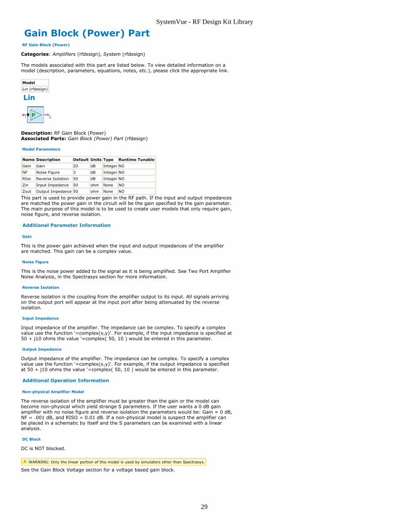
SystemVue - RF Design Kit Library
29
Gain Block (Power) Part RF Gain Block (Power)
Categories: Amplifiers (rfdesign), System (rfdesign)
The models associated with this part are listed below. To view detailed information on amodel (description, parameters, equations, notes, etc.), please click the appropriate link.
Model
Lin (rfdesign)
Lin
Description: RF Gain Block (Power)Associated Parts: Gain Block (Power) Part (rfdesign)
Model Parameters
Name Description Default Units Type Runtime Tunable
Gain Gain 20 dB Integer NO
NF Noise Figure 3 dB Integer NO
RIso Reverse Isolation 50 dB Integer NO
Zin Input Impedance 50 ohm None NO
Zout Output Impedance 50 ohm None NO
This part is used to provide power gain in the RF path. If the input and output impedancesare matched the power gain in the circuit will be the gain specified by the gain parameter.The main purpose of this model is to be used to create user models that only require gain,noise figure, and reverse isolation.
Additional Parameter Information
Gain
This is the power gain achieved when the input and output impedances of the amplifierare matched. This gain can be a complex value.
Noise Figure
This is the noise power added to the signal as it is being amplified. See Two Port AmplifierNoise Analysis, in the Spectrasys section for more information.
Reverse Isolation
Reverse isolation is the coupling from the amplifier output to its input. All signals arrivingon the output port will appear at the input port after being attenuated by the reverseisolation.
Input Impedance
Input impedance of the amplifier. The impedance can be complex. To specify a complexvalue use the function '=complex(x,y)'. For example, if the input impedance is specified at50 + j10 ohms the value '=complex( 50, 10 ) would be entered in this parameter.
Output Impedance
Output impedance of the amplifier. The impedance can be complex. To specify a complexvalue use the function '=complex(x,y)'. For example, if the output impedance is specifiedat 50 + j10 ohms the value '=complex( 50, 10 ) would be entered in this parameter.
Additional Operation Information
Non-physical Amplifier Model
The reverse isolation of the amplifier must be greater than the gain or the model canbecome non-physical which yield strange S parameters. If the user wants a 0 dB gainamplifier with no noise figure and reverse isolation the parameters would be: Gain = 0 dB,NF = .001 dB, and RISO = 0.01 dB. If a non-physical model is suspect the amplifier canbe placed in a schematic by itself and the S parameters can be examined with a linearanalysis.
DC Block
DC is NOT blocked.
WARNING: Only the linear portion of this model is used by simulators other than Spectrasys.
See the Gain Block Voltage section for a voltage based gain block.
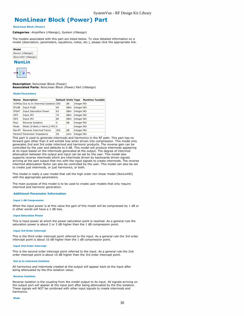
SystemVue - RF Design Kit Library
30
NonLinear Block (Power) Part NonLinear Block (Power)
Categories: Amplifiers (rfdesign), System (rfdesign)
The models associated with this part are listed below. To view detailed information on amodel (description, parameters, equations, notes, etc.), please click the appropriate link.
Model
NonLin (rfdesign)
NonLinHO (rfdesign)
NonLin
Description: NonLinear Block (Power)Associated Parts: NonLinear Block (Power) Part (rfdesign)
Model Parameters
Name Description Default Units Type Runtime Tunable
InIMIso Out to In Intermod Isolation 300 dB Integer NO
IP1dB Input P1dB 60 dBm Integer NO
IPSAT Input Saturation Power 63 dBm Integer NO
IIP3 Input IP3 70 dBm Integer NO
IIP2 Input IP2 80 dBm Integer NO
Riso Reverse Isolation 0 dB Integer NO
Mode Mode (0-Both,1-Harm,2-IM) 0 Integer NO
RevIM Reverse Intermod Factor 300 dB Integer NO
ParamZ Parameter Impedance 50 ohm Integer NO
This part is used to generate intermods and harmonics in the RF path. This part has noforward gain other than it will exhibit loss when driven into compression. This model onlygenerates 2nd and 3rd order intermod and harmonic products. The reverse gain can becontrolled by the user and defaults to 0 dB. This model will produce intermods appearingat its input based on the intermods generated at the output. The degree of intermodattenuation between the output and input can be set by the user. This model alsosupports reverse intermods which are intermods driven by backwards driven signalsarriving at the part output that mix with the input signals to create intermods. The reverseintermod attenuation factor can also be controlled by the user. This model can also be setto create just intermods, or just harmonics, or both.
This model is really a user model that call the high order non linear model (NonLinHO)with the appropriate parameters.
The main purpose of this model is to be used to create user models that only requireintermod and harmonic generation.
Additional Parameter Information
Input 1 dB Compression
When the input power is at this value the gain of this model will be compressed by 1 dB orin other words will have a 1 dB loss.
Input Saturation Power
This is input power at which the power saturation point is reached. As a general rule thesaturation power is about 2 or 3 dB higher than the 1 dB compression point.
Input 3rd Order Intercept
This is the third order intercept point referred to the input. As a general rule the 3rd orderintercept point is about 10 dB higher than the 1 dB compression point.
Input 2nd Order Intercept
This is the second order intercept point referred to the input. As a general rule the 2ndorder intercept point is about 10 dB higher than the 3rd order intercept point.
Out to In Intermod Isolation
All harmonics and intermods created at the output will appear back at the input afterbeing attenuated by the this isolation value.
Reverse Isolation
Reverse isolation is the coupling from the model output to its input. All signals arriving onthe output port will appear at the input port after being attenuated by the this isolation.These signals will NOT be combined with other input signals to create intermods andharmonics.
Mode

SystemVue - RF Design Kit Library
31
This determines the operating mode of the model. The mode can be set to just createharmonics, or just intermods, or both.
Reverse Intermod Factor
All signals driving the output of this model will be attenuated by this factor beforeappearing at the input. The sole purpose of these signals is to be used with the signalsdriving the model input to create intermods and harmonics. This is not to be confused withreverse isolation where those signals continue to propagate backwards through thesystem. All signals processed by this factor will not propagate past the input and are thenonly used to create intermods and harmonics. If this level is set sufficiently high all signalswill be attenuated below the 'Ignore Level Below' threshold and will never appear at theinput. These spectrum can be uniquely identified as 'RevIM' in the tooltip when themouse is placed over one of these spectrums in a spectral plot. This abbreviation standsfor reverse intermod source.
Parameter Impedance
This is the impedance at which the power of the IP1dB, IPSAT, IIP3, and IIP2 aredetermined. This parameter is only used to translate the power based non-linearparameters to voltage parameters that is used internally by the simulator.
Additional Operation Information
Compression
To accurately model compression in deep saturation several polynomial coefficients areneeded. Furthermore, polynomial stability in deep saturation can be an issue. In order tominimize the needed coefficients and improve the saturations stability in saturation anasymptotic polynomial approximation is used in this region. Intermod accuracy in thisregion is not guaranteed because a large polynomial is need to accurately represent thisregion and in most cases puts a huge burden on the user to find all of the coefficients.Furthermore, the simulation time will increase dramatically as the order is increased. Forthese reasons hyperbolic tangent functions are used to model compression to avoidpolynomial instabilities. Compression and saturation are defined to be based on a singleinput signal. Multiple input signals will have different compression characteristics. To verifythe compression point of the amplifier a single tone must be used.
Note: If the input saturation is greater than about 9 dB above the input 1 dB compression point thesaturation power will be set to 3 dB above the 1 dB compression point.
Output Intermod and Harmonic Phase
The output phase of an intermod is based on the phase of the input signals and thecoefficients of the intermod equation. However, the polynomial coefficients that representthe Vin versus Vout curve have negative coefficients for all odd orders 3 and higher. Thismeans that odd orders of 3 and higher will have a phase shift of 180 degrees. Thesenegative odd coefficients keep the transfer function from increasing monotonically. Output Phase = +/- K * Input1Phase +/- M * Input 2 Phase +/- N * Input 3 Phase ... Where K, M, N, etc are the coefficients of the intermod equation. For example, the phase of the 2nd harmonic will be double the input phase, triple theinput phase plus 180 degrees for a 3rd harmonic etc.
DC Block
DC is blocked.
WARNING: Only the linear portion of this model is used by simulators other than Spectrasys.
See the 'Non Linear Block Voltage' section for a voltage based nonlinear block.

SystemVue - RF Design Kit Library
32
NonLinear High Order Block (Power)Part NonLinear High Order Block (Power)
Categories: Amplifiers (rfdesign), System (rfdesign)
The models associated with this part are listed below. To view detailed information on amodel (description, parameters, equations, notes, etc.), please click the appropriate link.
Model
NonLinHO (rfdesign)
NonLinHO
Description: NonLinear Block (Power)Associated Parts: NonLinear Block (Power) Part (rfdesign)
Model Parameters
Name Description Default Units Type Runtime Tunable
InIMIso Out to In Intermod Isolation 300 dB Integer NO
IP1dB Input P1dB 60 dBm Integer NO
IPSAT Input Saturation Power 63 dBm Integer NO
IMN List of Intermods(IM1;IM2;IM3;...)
[0;-80;-140] dBm Integer NO
RISO Reverse Isolation 0 dB Integer NO
Mode Mode (0-Both,1-Harm,2-IM) 0 Integer NO
RevIM Reverse Intermod Factor 300 dB Integer NO
ParamZ Parameter Impedance 50 ohm Integer NO
This part is used to generate intermods and harmonics in the RF path. This part has noforward gain other than it will exhibit loss when driven into compression. This modelgenerates up to 20 orders of intermods and harmonic products. The reverse gain can becontrolled by the user and defaults to 0 dB. This model will produce intermods appearingat its input based on the intermods generated at the output. The degree of intermodattenuation between the output and input can be set by the user. This model alsosupports reverse intermods which are intermods driven by backwards driven signalsarriving at the part output that mix with the input signals to create intermods. The reverseintermod attenuation factor can also be controlled by the user. This model can also be setto create just intermods, or just harmonics, or both.
The coefficients of the polynomial are determined internally in the model from intermodinformation entered by the user. The intermod information can be easily measured in thelab or determined analytically. The maximum order supported by this model is 20.
The main purpose of this model is to be used to create user models that only requireintermod and harmonic generation.
Parameter Information
Input 1 dB Compression
When the input power is at this value the gain of this model will be compressed by 1 dB orin other words will have a 1 dB loss. See the Compression section for additionalinformation.
Input Saturation Power
This is input power at which the power saturation point is reached. As a general rule thesaturation power is about 2 or 3 dB higher than the 1 dB compression point.
Out to In Intermod Isolation
All harmonics and intermods created at the output will appear back at the input afterbeing attenuated by the this isolation value.
Reverse Isolation
Reverse isolation is the coupling from the model output to its input. All signals arriving onthe output port will appear at the input port after being attenuated by the this isolation.These signals will NOT be combined with other input signals to create intermods andharmonics.
Mode
This determines the operating mode of the model. The mode can be set to just createharmonics, or just intermods, or both.
Reverse Intermod Factor
All signals driving the output of this model will be attenuated by this factor before

SystemVue - RF Design Kit Library
33
appearing at the input. The sole purpose of these signals is to be used with the signalsdriving the model input to create intermods and harmonics. This is not to be confused withreverse isolation where those signals continue to propagate backwards through thesystem. All signals processed by this factor will not propagate past the input and are thenonly used to create intermods and harmonics. If this level is set sufficiently high all signalswill be attenuated below the 'Ignore Level Below (sim)' threshold and will never appear atthe input. These spectrum can be uniquely identified as 'RevIM' in the tooltip when themouse is placed over one of these spectrums in a spectral plot. This abbreviation standsfor reverse intermod source.
Parameter Impedance
This is the impedance at which the power of the IP1dB, IPSAT, and IMN are determined.This parameter is only used to translate the power based non-linear parameters to voltageparameters that is used internally by the simulator.
List of Intermods
This is list of intermods power levels in ascending order in dBm separated by semicolons (i.e. IM1 - intermod power level for 1st order intermod (fundamental), IM2 - intermodpower level for specific 2nd order intermods, IM3 - intermod power level for specific 3rdorder intermods, etc ). Not all intermods power levels need to be specified. However, allintermods up to the desired order need to be specified. Intermod power levels can bespecified in dBm or relative in dB. Internally the model will determine the power leveldifference in dB between IM1 and the corresponding intermod power level such as IM2,IM3, etc. This relative delta value is what is used internally to determine the interceptpoint for the respective order.
For example, if a user is only interested in the 3rd and 5th order products all five intermodpower levels are required (IM1;IM2;IM3;IM4;IM5). For this case IM2 and IM4 could beset to very low values (-1000) however, IM1 must be set since this is the fundamentaloutput of the amplifier and is a reference point for the rest of the intermods.
All intermod power levels should be measured in the region of desired operation of theamplifier but below amplifier saturation. The polynomial created in this case will be anexcellent approximation to that operating point of the amplifier. Remember, for non classA amplifiers the amplifier should also be driven above cutoff.
All intermods have a given amplitude coefficient. These coefficients are different for eachintermod combination. In order to correctly specify the intercept points for the respectiveorders arbitrary selected intermods for a given order cannot be used. Internally in themodel the following intermod table shows orders and their combinations that are used todetermine the intercept point. The intermod combinations in the following table all havethe same amplitude coefficients so theoretically any of these intermod combinations canbe used. Only 2 tones (F1 and F2) are needed to characterize these intermods. However,the user should remember that intermods with high frequencies may also be affected bythe frequency response of the amplifier as well as the measuring instrument and setup.
Name Order Combination 1 Combination 2 Combination 3 Combination 4
IM1 1 Fundamental
IM2 2 F1-F2 F1+F2
IM3 3 2F1-F2 F1-2F2 2F1+F2 F1+2F2
IM4 4 3F1-F2 F1-3F2 3F1+F2 F1+3F2
IM5 5 3F1-2F2 2F1-3F2 3F1+2F2 2F1+3F2
IM6 6 4F1-2F2 2F1-4F2 4F1+2F2 2F1+4F2
IM7 7 4F1-3F2 3F1-4F2 4F1+3F2 3F1+4F2
IM8 8 5F1-3F2 3F1-5F2 5F1+3F2 3F1+5F2
IM9 9 5F1-4F2 4F1-5F2 5F1+4F2 4F1+5F2
IM10 10 6F1-4F2 4F1-6F2 6F1+4F2 4F1+6F2
IM11 11 6F1-5F2 5F1-6F2 6F1+5F2 5F1+6F2
IM12 12 7F1-5F2 5F1-7F2 7F1+5F2 5F1+7F2
IM13 13 7F1-6F2 6F1-7F2 7F1+6F2 6F1+7F2
IM14 14 8F1-6F2 6F1-8F2 8F1+6F2 6F1+8F2
IM15 15 8F1-7F2 7F1-8F2 8F1+7F2 7F1+8F2
IM16 16 9F1-7F2 7F1-9F2 9F1+7F2 7F1+9F2
IM17 17 9F1-8F2 8F1-9F2 9F1+8F2 8F1+9F2
IM18 18 10F1-8F2 8F1-10F2 10F1+8F2 8F1+10F2
IM19 19 10F1-9F2 9F1-10F2 10F1+9F2 9F1+10F2
IM20 20 11F1-9F2 9F1-11F2 11F1+9F2 9F1+11F2
Guidelines For Intermod Measurements
The user can easily measure the needed intermod levels in a lab. In order to achieve thebest results please follow the given outline:
Select 2 frequencies that are in the band of interest.1.Assuming F1 < F2, then use the following formula to determine the spacing of F1and F2 so that the odd and even order intermod spectrum doesn't overlap. Remember, with current measurement techniques the user has no ability todistinguish one intermod from another at the same frequency. Consequently, thefrequency spacing between F1 and F2 must be wisely chosen to guarantee that weare looking at only the particular intermod of interest. Choose F1 and F2 to meet thefollowing condition.(Max Order)( F2 - F1 ) + F2 < 2F2For example: If the maximum order of interest was 10th and I was operating in the

SystemVue - RF Design Kit Library
34
150 MHz band then according to the formula, assuming F1 = 150 MHz and F2 = 160MHz:10( 160 - 150 ) + 160 < 2( 160 ) which becomes 260 < 320. This is a truestatement so the chosen 150 and 160 MHz signals will work fine.Apply the two input signals to the amplifier input using good intermodulation2.measurements techniques ( isolators, attenuators, splitters, etc. ). Set the powerlevel of the two input signals to the power level where the amplifier is to becharacterized. These power levels must be equal.The resolution bandwidth of the spectrum analyzer must be at least Max Order times3.the bandwidth of F1 or F2. But should be much less the spacing between F1 and F2.The amplifier output spectrum should appear as follows:4.
Measure the intermod power level of each point (IM1, IM2, IM3, ... ) and enter this5.into the model. You can easily verify that you have entered the correct values bycreating a simulation with a single amplifier using F1, F2, and the measured powerlevels. The Spectrum Analyzer Mode has been enabled to show the comparisonbetween what the spectrum analyzer will show and the actual intermod componentsthat make up the signal.
NOTE: The spectrum identification feature of Spectrasys is very helpful when choosing a test setup sinceyou can verify that the measured intermods, as specified in the above table, have a sufficient desiredintermod to undesired signal ratio to maintain accurate polynomial coefficients. Spectrum identificationcan also be used to identify the other intermod orders that are not shown in the plot.
Analytical Determination of Intermod Power Levels from Intercept Points
If the user knows the intercept points for the various orders due to two tones then thefollowing formulas can be used to determine the intermod power levels.
Since OIPn = IM1 + (IM1 - IMn ) / (n-1), where n is the order, OIPn is the outputintercept point due to two tones, and IMn is the intermod power level
Then solving for IMn:IMn = IM1 - (n-1) (OIPn - IM1)
If we choose:IM1 = 0
then:IMn = - (n-1) OIPn
For example if our OIP2 = +40 dBm and our OIP3 = +30 dBm
thenIM1 = 0 (this is our reference power level)IM2 = - (2-1) 40 = - 40IM3 = - (3-1) 30 = - 60
For the 'List of Intermods' in the amplifier model we would specify: ' 0; -40; -60 '. Ouramplifier would then generate all second and third order intermods.
Additional Operation Information
Compression
To accurately model compression in deep saturation several polynomial coefficients areneeded. Furthermore, polynomial stability in deep saturation can be an issue. In order tominimize the needed coefficients and improve the saturations stability in saturation anasymptotic polynomial approximation is used in this region. Intermod accuracy in thisregion is not guaranteed because a large polynomial is need to accurately represent thisregion and in most cases puts a huge burden on the user to find all of the coefficients.Furthermore, the simulation time will increase dramatically as the order is increased. Forthese reasons hyperbolic tangent functions are used to model compression to avoidpolynomial instabilities. Compression and saturation are defined to be based on a single

SystemVue - RF Design Kit Library
35
input signal. Multiple input signals will have different compression characteristics. To verifythe compression point of the amplifier a single tone must be used.
Note: If the input saturation is greater than about 9 dB above the input 1 dB compression point thesaturation power will be set to 3 dB above the 1 dB compression point.
Output Intermod and Harmonic Phase
The output phase of an intermod is based on the phase of the input signals and thecoefficients of the intermod equation. However, the polynomial coefficients that representthe Vin versus Vout curve have negative coefficients for all odd orders 3rd and higher.This means that odd orders of 3rd and higher will have a phase shift of 180 degrees.These negative odd coefficients keep the transfer function from increasing monotonically. Output Phase = +/- K * Input1Phase +/- M * Input 2 Phase +/- N * Input 3 Phase ... Where K, M, N, etc are the coefficients of the intermod equation. For example, the phase of the 2nd harmonic will be double the input phase, triple theinput phase plus 180 degrees for a 3rd harmonic etc.
DC Block
DC is blocked.
Orders Generated by Non-linear Section
Up to 20th order.
WARNING: Only the linear portion of this model is used by simulators other than Spectrasys.
See the 'Non Linear Block High Order Voltage' section for a voltage based nonlinear block.

SystemVue - RF Design Kit Library
36
Current Probe Part Current Probe (Ammeter). A device that detects an electric current.
Categories: Basic (rfdesign)
The models associated with this part are listed below. To view detailed information on amodel (description, parameters, equations, notes, etc.), please click the appropriate link.
Model
IPROBE (rfdesign)

SystemVue - RF Design Kit Library
37
RF IPROBE
Description: Current Probe (Ammeter). A device that detects an electric current.Associated Parts: Current Probe Part (rfdesign)
Model Parameters
Name Description Default Units Type Runtime Tunable
IDC DC Current 0 A Float NO
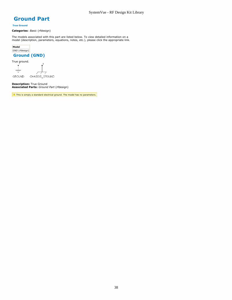
SystemVue - RF Design Kit Library
38
Ground Part True Ground
Categories: Basic (rfdesign)
The models associated with this part are listed below. To view detailed information on amodel (description, parameters, equations, notes, etc.), please click the appropriate link.
Model
GND (rfdesign)
Ground (GND)True ground.
Description: True GroundAssociated Parts: Ground Part (rfdesign)
This is simply a standard electrical ground. The model has no parameters.

SystemVue - RF Design Kit Library
39
Input(DC Curr) Part Input: DC Current
Categories: Basic (rfdesign)
The models associated with this part are listed below. To view detailed information on amodel (description, parameters, equations, notes, etc.), please click the appropriate link.
Model
INP_IDC (rfdesign)

SystemVue - RF Design Kit Library
40
RF INP IDC
Description: Input: DC CurrentAssociated Parts: Input(DC Curr) Part (rfdesign)
Model Parameters
Name Description Default Units Type Runtime Tunable
PORT Port Number 1 none Positiveinteger
NO
R Port Resistance 50 ohm Float NO
IDC DC Current 0 A Float NO

SystemVue - RF Design Kit Library
41
Input Part Input: Standard (*INP)
Categories: Basic (rfdesign)
The models associated with this part are listed below. To view detailed information on amodel (description, parameters, equations, notes, etc.), please click the appropriate link.
Model
INP (rfdesign)
Standard Input (*INP)The standard input port.
Description: Input: Standard (*INP)Associated Parts: Input Part (rfdesign)
Model Parameters
Name Description Default Units Type Runtime Tunable
ZO Impedance 50 ohm None NO
PORT Port Number 1 Positiveinteger
NO
Note: Use keyboard shortcut key "I" to place an input port in Schematic view.
Note: The port impedance is the impedance seen looking into the output port. If you specify a string valueas the impedance the string is interpreted as a 1 port datafile name. For example, a value of''Z:\MyFiles\VCO\VCO_IP_impedance.s1p" will tell SystemVue to read in that data file.

SystemVue - RF Design Kit Library
42
Output Port Part Output Port
Categories: Basic (rfdesign)
The models associated with this part are listed below. To view detailed information on amodel (description, parameters, equations, notes, etc.), please click the appropriate link.
Model
OUT (rfdesign)
Standard Output (*OUT)The standard output port.
Description: Output PortAssociated Parts: Output Port Part (rfdesign)
Model Parameters
Name Description Default Units Type Runtime Tunable
ZO Impedance 50 ohm None NO
PORT Port Number 2 Positiveinteger
NO
Note: Use keyboard shortcut key "O" to place an output port in Schematic View.
Note: The port impedance is the impedance seen looking into the output port. If you specify a string valueas the impedance the string is interpreted as a 1 port datafile name. For example, a value of''Z:\MyFiles\VCO\VCO_IP_impedance.s1p" will tell SystemVue to read in that data file.

SystemVue - RF Design Kit Library
43
Signal Ground Part Voltage/Current Sources
Categories: Basic (rfdesign)
The models associated with this part are listed below. To view detailed information on amodel (description, parameters, equations, notes, etc.), please click the appropriate link.
Model
VDC (rfdesign)

SystemVue - RF Design Kit Library
44
Source(DC Curr) Part Source: DC Current
Categories: Basic (rfdesign)
The models associated with this part are listed below. To view detailed information on amodel (description, parameters, equations, notes, etc.), please click the appropriate link.
Model
IDC (rfdesign)

SystemVue - RF Design Kit Library
45
RF IDC
Description: Source: DC CurrentAssociated Parts: Source(DC Curr) Part (rfdesign)
Model Parameters
Name Description Default Units Type Runtime Tunable
IDC DC Current 0.001 A Float NO

SystemVue - RF Design Kit Library
46
Source(DC Volt) Part Source: DC Voltage
Categories: Basic (rfdesign)
The models associated with this part are listed below. To view detailed information on amodel (description, parameters, equations, notes, etc.), please click the appropriate link.
Model
VDC (rfdesign)

SystemVue - RF Design Kit Library
47
RF VDC
Description: Source: DC VoltageAssociated Parts: Signal Ground Part (rfdesign), Source(DC Volt) Part (rfdesign)
Model Parameters
Name Description Default Units Type Runtime Tunable
VDC DC Voltage 1 V Float NO

SystemVue - RF Design Kit Library
48
Subcircuit (w 2-PortNoGnd) Part Subcircuit (N-Port w/2-PortNoGnd)
Categories: Basic (rfdesign)
The models associated with this part are listed below. To view detailed information on amodel (description, parameters, equations, notes, etc.), please click the appropriate link.
Model
RES (rfdesign)

SystemVue - RF Design Kit Library
49
Subcircuit (w NET2) Part Subcircuit (N-Port w/NET2)
Categories: Basic (rfdesign)
The models associated with this part are listed below. To view detailed information on amodel (description, parameters, equations, notes, etc.), please click the appropriate link.
Model
RES (rfdesign)

SystemVue - RF Design Kit Library
50
Test Point Part Voltage Test Point
Categories: Basic (rfdesign)
The models associated with this part are listed below. To view detailed information on amodel (description, parameters, equations, notes, etc.), please click the appropriate link.
Model
TEST_POINT (rfdesign)

SystemVue - RF Design Kit Library
51
RF TEST POINT
Description: Voltage Test PointAssociated Parts: Test Point Part (rfdesign)
Model Parameters
Name Description Default Units Type Runtime Tunable
VDC DC Voltage 0 V Float NO

SystemVue - RF Design Kit Library
52
Capacitor Part This is an ideal capacitor model.
Categories: Capacitors (rfdesign), Ideal (rfdesign), Lumped (rfdesign)
The models associated with this part are listed below. To view detailed information on amodel (description, parameters, equations, notes, etc.), please click the appropriate link.
Model
CAP (rfdesign)
CAPQ (rfdesign)
Capacitor (CAP)
Description: This is an ideal capacitor model.Associated Parts: Capacitor Part (rfdesign)
Model Parameters
Name Description Default Units Type Runtime Tunable
C Capacitance 10 pF Integer NO
Lumped capacitance model. Like many common parts, a short version of the symbol isavailable by holding the SHIFT key down while placing the part.
Note: Use the keyboard shortcut key "C" to place a capacitor.

SystemVue - RF Design Kit Library
53
CapacitorQ Part Capacitor with Q (CAPQ)
Categories: Capacitors (rfdesign), Ideal (rfdesign), Lumped (rfdesign)
The models associated with this part are listed below. To view detailed information on amodel (description, parameters, equations, notes, etc.), please click the appropriate link.
Model
CAPQ (rfdesign)
Capacitor with Q
Description: Capacitor with Q (CAPQ)Associated Parts: Capacitor Part (rfdesign), CapacitorQ Part (rfdesign)
Model Parameters
Name Description Default Units Type Runtime Tunable
C Capacitance 1000 pF Integer NO
QC Capacitor Q 1000000 Integer NO
F Frequency for Q 300 MHz Float NO
MODE 1:Prop to Freq,2:Prop tosqrt(f),3:Constant
3 Positiveinteger
NO
Lumped capacitance model with Q. Like many common parts, a short version of thesymbol is available by holding the SHIFT key down while placing the part.
Note: Use the keyboard shortcut key "C" to place a capacitor.

SystemVue - RF Design Kit Library
54
Coax Cable(RG6) Part RG6 Cable
Categories: Coax (rfdesign)
The models associated with this part are listed below. To view detailed information on amodel (description, parameters, equations, notes, etc.), please click the appropriate link.
Model
RG6 (rfdesign)
Coaxial Cable Type (RG6)
Description: RG6 CableAssociated Parts: Coax Cable(RG6) Part (rfdesign)
Model Parameters
Name Description Default Units Type Runtime Tunable
L Length 1000 mm Float NO
Z0 Characteristic Impedance 75 ohm Float NO
Er Dielectric Constant 1.78 none Float NO
kdb1 attn/m, per sqrt 0.006734 none Float NO
kdb2 attn/m, per MHz 0.0 none Float NO
RangeSingle part models are available for six widely used cable types: RG-6, 8, 9, 58, 59, 214.These have a characteristic impedance of 50 ohms, except for RG-6 and RG-59 which are75 ohms. In the Examples is a workspace, Coaxial_Cable.wsp, which presents a methodfor computing the required parameters from manufacturers data. It assumes that thecharacteristic impedance is readily available. The dielectric constant of the materialbetween the inner and outer conductors is commonly given. This can also be computed ifthe "velocity factor (Vp)" or "velocity of propagation" is given. The dielectric constant (Er)equals:
Er = ( 1 / Vp 2 ).
The attenuation parameters are may be available. If not, they can be calculated from thecurves of attenuation per 100 meters as a function of frequency. The example workspacefacilitates the curve fit.
For the six parts included, the default parameters are listed in the following table:
RG6 RG8 RG9 RG58 RG59 RG214
Zo 75.0 52.0 51.0 53.5 75.0 50.0
Er 1.78 2.26 2.26 2.26 1.45 2.26
Kdb1 .006734 .005264 .006229 .0138 .0085535 .00426
Kdb2 0 .69e-4 .70e-4 .1254e-3 0 0.1348e-3

SystemVue - RF Design Kit Library
55
Coax Cable(RG8) Part RG8 Cable
Categories: Coax (rfdesign)
The models associated with this part are listed below. To view detailed information on amodel (description, parameters, equations, notes, etc.), please click the appropriate link.
Model
RG8 (rfdesign)
Coaxial Cable Type (RG8)
Description: RG8 CableAssociated Parts: Coax Cable(RG8) Part (rfdesign)
Model Parameters
Name Description Default Units Type Runtime Tunable
L Length 1000 mm Float NO
Z0 Characteristic Impedance 52 ohm Float NO
Er Dielectric Constant 2.26 none Float NO
kdb1 attn/m, per sqrt 0.005264 none Float NO
kdb2 attn/m, per MHz 0.69e-4 none Float NO
RangeSingle part models are available for six widely used cable types: RG-6, 8, 9, 58, 59, 214.These have a characteristic impedance of 50 ohms, except for RG-6 and RG-59 which are75 ohms. In the Examples is a workspace, Coaxial_Cable.wsp, which presents a methodfor computing the required parameters from manufacturers data. It assumes that thecharacteristic impedance is readily available. The dielectric constant of the materialbetween the inner and outer conductors is commonly given. This can also be computed ifthe "velocity factor (Vp)" or "velocity of propagation" is given. The dielectric constant (Er)equals:
Er = ( 1 / Vp 2 ).
The attenuation parameters are may be available. If not, they can be calculated from thecurves of attenuation per 100 meters as a function of frequency. The example workspacefacilitates the curve fit.
For the six parts included, the default parameters are listed in the following table:
RG6 RG8 RG9 RG58 RG59 RG214
Zo 75.0 52.0 51.0 53.5 75.0 50.0
Er 1.78 2.26 2.26 2.26 1.45 2.26
Kdb1 .006734 .005264 .006229 .0138 .0085535 .00426
Kdb2 0 .69e-4 .70e-4 .1254e-3 0 0.1348e-3

SystemVue - RF Design Kit Library
56
Coax Cable(RG9) Part RG9 Cable
Categories: Coax (rfdesign)
The models associated with this part are listed below. To view detailed information on amodel (description, parameters, equations, notes, etc.), please click the appropriate link.
Model
RG9 (rfdesign)
Coaxial Cable Type (RG9)
Description: RG9 CableAssociated Parts: Coax Cable(RG9) Part (rfdesign)
Model Parameters
Name Description Default Units Type Runtime Tunable
L Length 1000 mm Float NO
Z0 Characteristic Impedance 51 ohm Float NO
Er Dielectric Constant 2.26 none Float NO
kdb1 attn/m, per sqrt 0.006229 none Float NO
kdb2 attn/m, per MHz 0.70e-4 none Float NO
RangeSingle part models are available for six widely used cable types: RG-6, 8, 9, 58, 59, 214.These have a characteristic impedance of 50 ohms, except for RG-6 and RG-59 which are75 ohms. In the Examples is a workspace, Coaxial_Cable.wsp, which presents a methodfor computing the required parameters from manufacturers data. It assumes that thecharacteristic impedance is readily available. The dielectric constant of the materialbetween the inner and outer conductors is commonly given. This can also be computed ifthe "velocity factor (Vp)" or "velocity of propagation" is given. The dielectric constant (Er)equals:
Er = ( 1 / Vp 2 ).
The attenuation parameters are may be available. If not, they can be calculated from thecurves of attenuation per 100 meters as a function of frequency. The example workspacefacilitates the curve fit.
For the six parts included, the default parameters are listed in the following table:
RG6 RG8 RG9 RG58 RG59 RG214
Zo 75.0 52.0 51.0 53.5 75.0 50.0
Er 1.78 2.26 2.26 2.26 1.45 2.26
Kdb1 .006734 .005264 .006229 .0138 .0085535 .00426
Kdb2 0 .69e-4 .70e-4 .1254e-3 0 0.1348e-3

SystemVue - RF Design Kit Library
57
Coax Cable(RG58) Part RG58 Cable
Categories: Coax (rfdesign)
The models associated with this part are listed below. To view detailed information on amodel (description, parameters, equations, notes, etc.), please click the appropriate link.
Model
RG58 (rfdesign)
Coaxial Cable Type (RG58)
Description: RG58 CableAssociated Parts: Coax Cable(RG58) Part (rfdesign)
Model Parameters
Name Description Default Units Type Runtime Tunable
L Length 25.4 mm Float NO
Z0 Characteristic Impedance 53.5 ohm Float NO
Er Dielectric Constant 2.26 none Float NO
kdb1 attn/m, per sqrt 0.014 none Float NO
kdb2 attn/m, per MHz 0 none Float NO
RangeSingle part models are available for six widely used cable types: RG-6, 8, 9, 58, 59, 214.These have a characteristic impedance of 50 ohms, except for RG-6 and RG-59 which are75 ohms. In the Examples is a workspace, Coaxial_Cable.wsp, which presents a methodfor computing the required parameters from manufacturers data. It assumes that thecharacteristic impedance is readily available. The dielectric constant of the materialbetween the inner and outer conductors is commonly given. This can also be computed ifthe "velocity factor (Vp)" or "velocity of propagation" is given. The dielectric constant (Er)equals:
Er = ( 1 / Vp 2 ).
The attenuation parameters are may be available. If not, they can be calculated from thecurves of attenuation per 100 meters as a function of frequency. The example workspacefacilitates the curve fit.
For the six parts included, the default parameters are listed in the following table:
RG6 RG8 RG9 RG58 RG59 RG214
Zo 75.0 52.0 51.0 53.5 75.0 50.0
Er 1.78 2.26 2.26 2.26 1.45 2.26
Kdb1 .006734 .005264 .006229 .0138 .0085535 .00426
Kdb2 0 .69e-4 .70e-4 .1254e-3 0 0.1348e-3
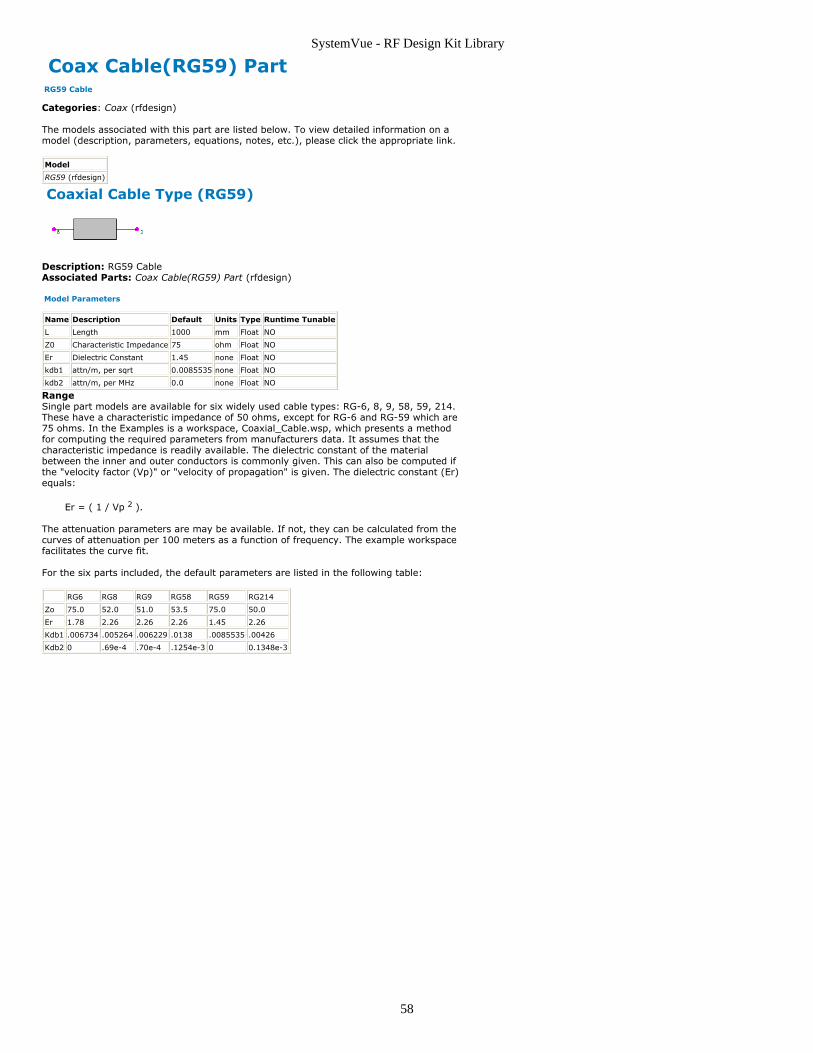
SystemVue - RF Design Kit Library
58
Coax Cable(RG59) Part RG59 Cable
Categories: Coax (rfdesign)
The models associated with this part are listed below. To view detailed information on amodel (description, parameters, equations, notes, etc.), please click the appropriate link.
Model
RG59 (rfdesign)
Coaxial Cable Type (RG59)
Description: RG59 CableAssociated Parts: Coax Cable(RG59) Part (rfdesign)
Model Parameters
Name Description Default Units Type Runtime Tunable
L Length 1000 mm Float NO
Z0 Characteristic Impedance 75 ohm Float NO
Er Dielectric Constant 1.45 none Float NO
kdb1 attn/m, per sqrt 0.0085535 none Float NO
kdb2 attn/m, per MHz 0.0 none Float NO
RangeSingle part models are available for six widely used cable types: RG-6, 8, 9, 58, 59, 214.These have a characteristic impedance of 50 ohms, except for RG-6 and RG-59 which are75 ohms. In the Examples is a workspace, Coaxial_Cable.wsp, which presents a methodfor computing the required parameters from manufacturers data. It assumes that thecharacteristic impedance is readily available. The dielectric constant of the materialbetween the inner and outer conductors is commonly given. This can also be computed ifthe "velocity factor (Vp)" or "velocity of propagation" is given. The dielectric constant (Er)equals:
Er = ( 1 / Vp 2 ).
The attenuation parameters are may be available. If not, they can be calculated from thecurves of attenuation per 100 meters as a function of frequency. The example workspacefacilitates the curve fit.
For the six parts included, the default parameters are listed in the following table:
RG6 RG8 RG9 RG58 RG59 RG214
Zo 75.0 52.0 51.0 53.5 75.0 50.0
Er 1.78 2.26 2.26 2.26 1.45 2.26
Kdb1 .006734 .005264 .006229 .0138 .0085535 .00426
Kdb2 0 .69e-4 .70e-4 .1254e-3 0 0.1348e-3
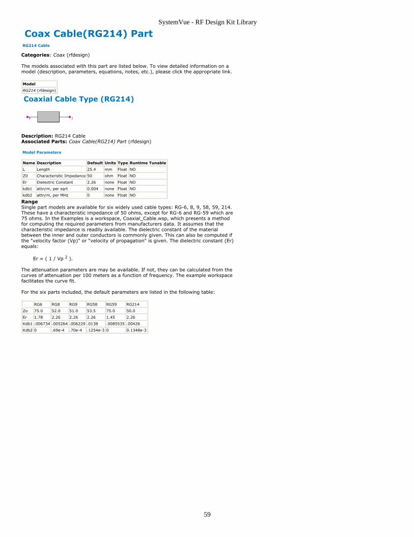
SystemVue - RF Design Kit Library
59
Coax Cable(RG214) Part RG214 Cable
Categories: Coax (rfdesign)
The models associated with this part are listed below. To view detailed information on amodel (description, parameters, equations, notes, etc.), please click the appropriate link.
Model
RG214 (rfdesign)
Coaxial Cable Type (RG214)
Description: RG214 CableAssociated Parts: Coax Cable(RG214) Part (rfdesign)
Model Parameters
Name Description Default Units Type Runtime Tunable
L Length 25.4 mm Float NO
Z0 Characteristic Impedance 50 ohm Float NO
Er Dielectric Constant 2.26 none Float NO
kdb1 attn/m, per sqrt 0.004 none Float NO
kdb2 attn/m, per MHz 0 none Float NO
RangeSingle part models are available for six widely used cable types: RG-6, 8, 9, 58, 59, 214.These have a characteristic impedance of 50 ohms, except for RG-6 and RG-59 which are75 ohms. In the Examples is a workspace, Coaxial_Cable.wsp, which presents a methodfor computing the required parameters from manufacturers data. It assumes that thecharacteristic impedance is readily available. The dielectric constant of the materialbetween the inner and outer conductors is commonly given. This can also be computed ifthe "velocity factor (Vp)" or "velocity of propagation" is given. The dielectric constant (Er)equals:
Er = ( 1 / Vp 2 ).
The attenuation parameters are may be available. If not, they can be calculated from thecurves of attenuation per 100 meters as a function of frequency. The example workspacefacilitates the curve fit.
For the six parts included, the default parameters are listed in the following table:
RG6 RG8 RG9 RG58 RG59 RG214
Zo 75.0 52.0 51.0 53.5 75.0 50.0
Er 1.78 2.26 2.26 2.26 1.45 2.26
Kdb1 .006734 .005264 .006229 .0138 .0085535 .00426
Kdb2 0 .69e-4 .70e-4 .1254e-3 0 0.1348e-3

SystemVue - RF Design Kit Library
60
Coax Cable Part Coaxial Cable
Categories: Coax (rfdesign)
The models associated with this part are listed below. To view detailed information on amodel (description, parameters, equations, notes, etc.), please click the appropriate link.
Model
CABLE (rfdesign)
Coaxial Cable (CABLE)
Description: Coaxial CableAssociated Parts: Coax Cable Part (rfdesign)
Model Parameters
Name Description Default Units Type Runtime Tunable
L Length none mm Integer NO
Z0 Characteristic Impedance none ohm Integer NO
Er Dielectric Constant none Integer NO
kdb1 attn/m, per sqrt|MHz none Integer NO
kdb2 attn/m, per MHz none Integer NO
Range:Single part models are available for six widely used cable types: RG-6, 8, 9, 58, 59, 214.These have a characteristic impedance of 50 ohms, except for RG-6 and RG-59 which are75 ohms. In the Examples is a workspace, Coaxial_Cable.wsp, which presents a methodfor computing the required parameters from manufacturers data. It assumes that thecharacteristic impedance is readily available. The dielectric constant of the materialbetween the inner and outer conductors is commonly given. This can also be computed ifthe "velocity factor (Vp)" or "velocity of propagation" is given. The dielectric constant (Er)equals:
Er = ( 1 / Vp 2 ).
The attenuation parameters are may be available. If not, they can be calculated from thecurves of attenuation per 100 meters as a function of frequency. The example workspacefacilitates the curve fit.
SystemVue - RF Design Kit Library
61
Bandpass Filter(Bessel) Part Bandpass Bessel Filter
Categories: Filters (rfdesign), System (rfdesign)
The models associated with this part are listed below. To view detailed information on amodel (description, parameters, equations, notes, etc.), please click the appropriate link.
Model
BPF_BESSEL (rfdesign)
BPF_BESSEL_C (rfdesign)
BPF_BESSEL
Description: Bandpass Bessel FilterAssociated Parts: Bandpass Filter(Bessel) Part (rfdesign)
Model Parameters
Name Description Default Units Type Runtime Tunable
IL Insertion Loss 0.01 dB Integer NO
N Filter Order 3 Integer NO
Flo Lower Passband Edge Frequency 90.0 MHz Integer NO
Fhi Higher Passband Edge Frequency 100.0 MHz Integer NO
Apass Attenuation at Passband 3.0103 dB Integer NO
Amax Max Attenuation in stopband 100.0 dB Integer NO
Z1 Ref Impedance Port 1 50.0 ohm Integer NO
Z2 Ref Impedance Port 2, (Default=Z1) 50.0 ohm Integer NO
TYPE Input Stopband Impedance 0-short,1-open 1 Integer NO
This part is used to provide filtering in the RF path. This system symbol is available on theSystem toolbar.
NOTE: The alternate model "..._C" is a circuit model created from a synthesis process with realcomponents. The circuit is not visible to the user. Simulation time for the circuit models is generally longersince there are more components.
Additional Parameter/Operation Information
The Bessel filter characteristic has a flat group delay response in the passbandgenerated by poles only. This results in no ripple in the passband, but a cutoff whichis less sharp than some other filters. The insertion loss only affects the forward (S 21
) and backward (S 12 ) transmission, but not the reflection coefficients (S 11 ,S 22 ).
The input impedance in the stopband only affects the phase of the reflectioncoefficients. For additional details on filter types see the FILTER Synthesis Manual.
Note: The insertion loss and passband attenuation must be greater or equal to zero. The filter order mustbe an integer greater or equal to 1. The frequencies of the passband edges must be positive and thehigher frequency must be larger than the lower frequency.
DC Block - DC is blocked.
Maximum Attenuation in stopband - The maximum attenuation in the stopband ismodeled with a resistor between the input and output port of the filter. An equationis used to determine the value of the resistor from the given attenuation. Thisparallel resistor will only be effective when the filter stopband impedance TYPE is setto open. For even filter orders the impedance looking into one port is high and theother low so the maximum attenuation in the stopband has no effect.
BPF_BESSEL_C
Description: Bandpass Bessel FilterAssociated Parts: Bandpass Filter(Bessel) Part (rfdesign)
Model Parameters
Name Description Default Units Type Runtime Tunable
IL Insertion Loss 0.01 dB Integer NO
N Filter Order 3 Integer NO
Flo Lower Passband Edge Frequency 90.0 MHz Integer NO
Fhi Higher Passband Edge Frequency 100.0 MHz Integer NO
Apass Attenuation at Passband 3.0103 dB Integer NO
Amax Max Attenuation in stopband 100.0 dB Integer NO
Z1 Ref Impedance Port 1 50.0 ohm Integer NO
Z2 Ref Impedance Port 2, (Default=Z1) 50.0 ohm Integer NO
TYPE Input Stopband Impedance 0-short,1-open 1 Integer NO

SystemVue - RF Design Kit Library
62
Bandpass Filter(Butterworth) Part Bandpass Butterworth Filter
Categories: Filters (rfdesign), System (rfdesign)
The models associated with this part are listed below. To view detailed information on amodel (description, parameters, equations, notes, etc.), please click the appropriate link.
Model
BPF_BUTTER (rfdesign)
BPF_BUTTER_C (rfdesign)
BPF_BUTTER
Description: Bandpass Butterworth FilterAssociated Parts: Bandpass Filter(Butterworth) Part (rfdesign)
Model Parameters
Name Description Default Units Type Runtime Tunable
IL Insertion Loss 0.01 dB Integer NO
N Filter Order 3 Integer NO
Flo Lower Passband Edge Frequency 90.0 MHz Integer NO
Fhi Higher Passband Edge Frequency 100.0 MHz Integer NO
Apass Attenuation at Passband 3.0103 dB Integer NO
Amax Max Attenuation in stopband 100.0 dB Integer NO
Z1 Ref Impedance Port 1 50.0 ohm Integer NO
Z2 Ref Impedance Port 2, (Default=Z1) 50.0 ohm Integer NO
TYPE Input Stopband Impedance 0-short,1-open 1 Integer NO
This part is used to provide filtering in the RF path. This system symbol is available on theSystem toolbar.
NOTE: The alternate model "..._C" is a circuit model created from a synthesis process with realcomponents. The circuit is not visible to the user. Simulation time for the circuit models is generally longersince there are more components.
Additional Parameter/Operation Information
The Butterworth filter characteristic is a maximally flat response in the passbandgenerated by poles only. This results in no ripple in the passband, but a cutoff whichis less sharp than some other filters. The insertion loss only affects the forward (S 21
) and backward (S 12 ) transmission, but not the reflection coefficients (S 11 ,S 22 ).
The input impedance in the stopband only affects the phase of the reflectioncoefficients. For additional details on filter types see the FILTER Synthesis Manual.
Note: The insertion loss and passband attenuation must be greater or equal to zero. The filter order mustbe an integer greater or equal to 1. The frequencies of the passband edges must be positive and thehigher frequency must be larger than the lower frequency.
DC Block - DC is blocked.
Maximum Attenuation in stopband - The maximum attenuation in the stopband ismodeled with a resistor between the input and output port of the filter. An equationis used to determine the value of the resistor from the given attenuation. Thisparallel resistor will only be effective when the filter stopband impedance TYPE is setto open. For even filter orders the impedance looking into one port is high and theother low so the maximum attenuation in the stopband has no effect.
BPF_BUTTER_C
Description: Bandpass Butterworth FilterAssociated Parts: Bandpass Filter(Butterworth) Part (rfdesign)
Model Parameters
Name Description Default Units Type Runtime Tunable
IL Insertion Loss 0.01 dB Integer NO
N Filter Order 3 Integer NO
Flo Lower Passband Edge Frequency 90.0 MHz Integer NO
Fhi Higher Passband Edge Frequency 100.0 MHz Integer NO
Apass Attenuation at Passband 3.0103 dB Integer NO
Amax Max Attenuation in stopband 100.0 dB Integer NO
Z1 Ref Impedance Port 1 50.0 ohm Integer NO
Z2 Ref Impedance Port 2, (Default=Z1) 50.0 ohm Integer NO
TYPE Input Stopband Impedance 0-short,1-open 1 Integer NO

SystemVue - RF Design Kit Library
63
Bandpass Filter(Chebyshev) Part Bandpass Chebyshev Filter
Categories: Filters (rfdesign), System (rfdesign)
The models associated with this part are listed below. To view detailed information on amodel (description, parameters, equations, notes, etc.), please click the appropriate link.
Model
BPF_CHEBY (rfdesign)
BPF_CHEBY_C (rfdesign)
BPF_CHEBY
Description: Bandpass Chebyshev FilterAssociated Parts: Bandpass Filter(Chebyshev) Part (rfdesign)
Model Parameters
Name Description Default Units Type Runtime Tunable
IL Insertion Loss 0.01 dB Integer NO
N Filter Order 3 Integer NO
R Ripple 0.1 dB Integer NO
Flo Lower Passband Edge Frequency 90.0 MHz Integer NO
Fhi Higher Passband Edge Frequency 100.0 MHz Integer NO
Apass Attenuation at Passband 0.1 dB Integer NO
Amax Max Attenuation in stopband 100.0 dB Integer NO
Z1 Ref Impedance Port 1 50.0 ohm Integer NO
Z2 Ref Impedance Port 2, (Default=Z1) 50.0 ohm Integer NO
TYPE Input Stopband Impedance 0-short,1-open 1 Integer NO
This part is used to provide filtering in the RF path.
NOTE: The alternate model "..._C" is a circuit model created from a synthesis process with realcomponents. The circuit is not visible to the user. Simulation time for the circuit models is generally longersince there are more components.
Additional Parameter/Operation Information
The Chebyshev filter characteristic exhibits ripple in the passband and generated bypoles only. This results in a cutoff which is sharper than some other filters. Theinsertion loss only affects the forward (S 21 ) and backward (S 12 ) transmission, but
not the reflection coefficients (S 11 ,S 22 ). The input impedance in the stopband only
affects the phase of the reflection coefficients. The nominal value for the attenuationat the passband edge (Apass) is the ripple value. For filters of even order, the gain atdc is less than unity to avoid gains greater than unity in the passband. For additionaldetails on filter types see the FILTER Synthesis Manual.
Note: The insertion loss and passband attenuation must be greater or equal to zero. The filter order mustbe an integer greater or equal to 2. The frequency of the passband edges must be positive and the higherfrequency must be larger than the lower frequency.
DC Block - DC is blocked.
Maximum Attenuation in stopband - The maximum attenuation in the stopband ismodeled with a resistor between the input and output port of the filter. An equationis used to determine the value of the resistor from the given attenuation. Thisparallel resistor will only be effective when the filter stopband impedance TYPE is setto open. For even filter orders the impedance looking into one port is high and theother low so the maximum attenuation in the stopband has no effect.
BPF_CHEBY_C
Description: Bandpass Chebyshev FilterAssociated Parts: Bandpass Filter(Chebyshev) Part (rfdesign)
Model Parameters

SystemVue - RF Design Kit Library
64
Name Description Default Units Type Runtime Tunable
IL Insertion Loss 0.01 dB Integer NO
N Filter Order 3 Integer NO
R Ripple 0.1 dB Integer NO
Flo Lower Passband Edge Frequency 90.0 MHz Integer NO
Fhi Higher Passband Edge Frequency 100.0 MHz Integer NO
Apass Attenuation at Passband 0.1 dB Integer NO
Amax Max Attenuation in stopband 100.0 dB Integer NO
Z1 Ref Impedance Port 1 50.0 ohm Integer NO
Z2 Ref Impedance Port 2, (Default=Z1) 50.0 ohm Integer NO
TYPE Input Stopband Impedance 0-short,1-open 1 Integer NO

SystemVue - RF Design Kit Library
65
Bandpass Filter(Elliptic) Part Bandpass Elliptic Filter
Categories: Filters (rfdesign), System (rfdesign)
The models associated with this part are listed below. To view detailed information on amodel (description, parameters, equations, notes, etc.), please click the appropriate link.
Model
BPF_ELLIPTIC (rfdesign)
BPF_ELLIPTIC_C (rfdesign)
BPF_ELLIPTIC
Description: Bandpass Elliptic FilterAssociated Parts: Bandpass Filter(Elliptic) Part (rfdesign)
Model Parameters
Name Description Default Units Type Runtime Tunable
IL Insertion Loss 0.01 dB Integer NO
N Filter Order 3 Integer NO
R Ripple 0.1 dB Integer NO
SBATTN Stopband Attenuation 40.0 dB Integer NO
Flo Lower Passband Edge Frequency 90.0 MHz Integer NO
Fhi Higher Passband Edge Frequency 100.0 MHz Integer NO
Amax Max Attenuation in stopband 100.0 dB Integer NO
Z1 Ref Impedance Port 1 50.0 ohm Integer NO
Z2 Ref Impedance Port 2, (Default=Z1) 50.0 ohm Integer NO
TYPE Input Stopband Impedance 0-short,1-open 1 Integer NO
This part is used to provide filtering in the RF path.
NOTE: The alternate model "..._C" is a circuit model created from a synthesis process with realcomponents. The circuit is not visible to the user. Simulation time for the circuit models is generally longersince there are more components.
Additional Parameter/Operation Information
The Elliptic filter characteristic exhibits ripple in the passband and generated by polesand zeros. This results in a cutoff which is sharper than most other filters. Theinsertion loss only affects the forward (S 21 ) and backward (S 12 ) transmission, but
not the reflection coefficients (S 11 ,S 22 ). The input impedance in the stopband only
affects the phase of the reflection coefficients. The value for the attenuation at thepassband edge (Apass) is the ripple value. For filters of even order, the gain at dc isless than unity to avoid gains greater than unity in the passband. For additionaldetails on filter types see the FILTER Synthesis Manual.
Note: The insertion loss must be greater or equal to zero. The filter order must be an integer greater orequal to 2. The frequencies of the passband edges must be positive and the higher frequency must belarger than the lower frequency. The stopband attenuation must be greater than the ripple.
DC Block - DC is blocked.
Maximum Attenuation in stopband - The maximum attenuation in the stopband ismodeled with a resistor between the input and output port of the filter. An equationis used to determine the value of the resistor from the given attenuation. Thisparallel resistor will only be effective when the filter stopband impedance TYPE is setto open. For even filter orders the impedance looking into one port is high and theother low so the maximum attenuation in the stopband has no effect.
BPF_ELLIPTIC_C
Description: Bandpass Elliptic FilterAssociated Parts: Bandpass Filter(Elliptic) Part (rfdesign)
Model Parameters

SystemVue - RF Design Kit Library
66
Name Description Default Units Type Runtime Tunable
IL Insertion Loss 0.01 dB Integer NO
N Filter Order 3 Integer NO
R Ripple 0.1 dB Integer NO
SBATTN Stopband Attenuation 40.0 dB Integer NO
Flo Lower Passband Edge Frequency 90.0 MHz Integer NO
Fhi Higher Passband Edge Frequency 100.0 MHz Integer NO
Amax Max Attenuation in stopband 100.0 dB Integer NO
Z1 Ref Impedance Port 1 50.0 ohm Integer NO
Z2 Ref Impedance Port 2, (Default=Z1) 50.0 ohm Integer NO
TYPE Input Stopband Impedance 0-short,1-open 1 Integer NO
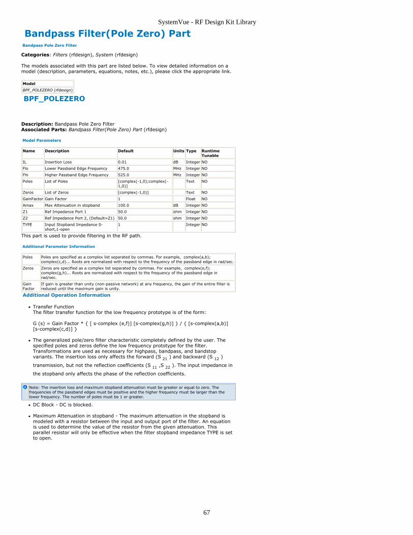
SystemVue - RF Design Kit Library
67
Bandpass Filter(Pole Zero) Part Bandpass Pole Zero Filter
Categories: Filters (rfdesign), System (rfdesign)
The models associated with this part are listed below. To view detailed information on amodel (description, parameters, equations, notes, etc.), please click the appropriate link.
Model
BPF_POLEZERO (rfdesign)
BPF_POLEZERO
Description: Bandpass Pole Zero FilterAssociated Parts: Bandpass Filter(Pole Zero) Part (rfdesign)
Model Parameters
Name Description Default Units Type RuntimeTunable
IL Insertion Loss 0.01 dB Integer NO
Flo Lower Passband Edge Frequency 475.0 MHz Integer NO
Fhi Higher Passband Edge Frequency 525.0 MHz Integer NO
Poles List of Poles [complex(-1,0);complex(-1,0)]
Text NO
Zeros List of Zeros [complex(-1,0)] Text NO
GainFactor Gain Factor 1 Float NO
Amax Max Attenuation in stopband 100.0 dB Integer NO
Z1 Ref Impedance Port 1 50.0 ohm Integer NO
Z2 Ref Impedance Port 2, (Default=Z1) 50.0 ohm Integer NO
TYPE Input Stopband Impedance 0-short,1-open
1 Integer NO
This part is used to provide filtering in the RF path.
Additional Parameter Information
Poles Poles are specified as a complex list separated by commas. For example, complex(a,b);complex(c,d)... Roots are normalized with respect to the frequency of the passband edge in rad/sec.
Zeros Zeros are specified as a complex list separated by commas. For example, complex(e,f);complex(g,h)... Roots are normalized with respect to the frequency of the passband edge inrad/sec.
GainFactor
If gain is greater than unity (non-passive network) at any frequency, the gain of the entire filter isreduced until the maximum gain is unity.
Additional Operation Information
Transfer FunctionThe filter transfer function for the low frequency prototype is of the form: G (s) = Gain Factor * { [ s-complex (e,f)] [s-complex(g,h)] } / { [s-complex(a,b)][s-complex(c,d)] }
The generalized pole/zero filter characteristic completely defined by the user. Thespecified poles and zeros define the low frequency prototype for the filter.Transformations are used as necessary for highpass, bandpass, and bandstopvariants. The insertion loss only affects the forward (S 21 ) and backward (S 12 )
transmission, but not the reflection coefficients (S 11 ,S 22 ). The input impedance in
the stopband only affects the phase of the reflection coefficients.
Note: The insertion loss and maximum stopband attenuation must be greater or equal to zero. Thefrequencies of the passband edges must be positive and the higher frequency must be larger than thelower frequency. The number of poles must be 1 or greater.
DC Block - DC is blocked.
Maximum Attenuation in stopband - The maximum attenuation in the stopband ismodeled with a resistor between the input and output port of the filter. An equationis used to determine the value of the resistor from the given attenuation. Thisparallel resistor will only be effective when the filter stopband impedance TYPE is setto open.

SystemVue - RF Design Kit Library
68
Bandstop Filter(Bessel) Part Bandstop Bessel Filter
Categories: Filters (rfdesign), System (rfdesign)
The models associated with this part are listed below. To view detailed information on amodel (description, parameters, equations, notes, etc.), please click the appropriate link.
Model
BSF_BESSEL (rfdesign)
BSF_BESSEL_C (rfdesign)
BSF_BESSEL
Description: Bandstop Bessel FilterAssociated Parts: Bandstop Filter(Bessel) Part (rfdesign)
Model Parameters
Name Description Default Units Type Runtime Tunable
IL Insertion Loss 0.01 dB Integer NO
N Filter Order 3 Integer NO
Flo Lower Passband Edge Frequency 475.0 MHz Integer NO
Fhi Higher Passband Edge Frequency 525.0 MHz Integer NO
Apass Attenuation at Passband 3.0103 dB Integer NO
Amax Max Attenuation in stopband 100.0 dB Integer NO
Z1 Ref Impedance Port 1 50.0 ohm Integer NO
Z2 Ref Impedance Port 2, (Default=Z1) 50.0 ohm Integer NO
TYPE Input Stopband Impedance 0-short,1-open 0 Integer NO
This part is used to provide filtering in the RF path.
NOTE: The alternate model "..._C" is a circuit model created from a synthesis process with realcomponents. The circuit is not visible to the user. Simulation time for the circuit models is generally longersince there are more components.
Additional Parameter/Operation Information
The Bessel filter characteristic has a flat group delay response in the passbandgenerated by poles only. This results in no ripple in the passband, but a cutoff whichis less sharp than some other filters. The insertion loss only affects the forward (S 21
) and backward (S 12 ) transmission, but not the reflection coefficients (S 11 ,S 22 ).
The input impedance in the stopband only affects the phase of the reflectioncoefficients. For additional details on filter types see the FILTER Synthesis Manual.
Note: The insertion loss and passband attenuation must be greater or equal to zero. The filter order mustbe an integer greater or equal to 1. The frequencies of the passband edges must be positive and thehigher frequency must be larger than the lower frequency.
DC Block - DC is passed.
Maximum Attenuation in stopband - The maximum attenuation in the stopband ismodeled with a resistor between the input and output port of the filter. An equationis used to determine the value of the resistor from the given attenuation. Thisparallel resistor will only be effective when the filter stopband impedance TYPE is setto open. For even filter orders the impedance looking into one port is high and theother low so the maximum attenuation in the stopband has no effect.
BSF_BESSEL_C
Description: Bandstop Bessel FilterAssociated Parts: Bandstop Filter(Bessel) Part (rfdesign)
Model Parameters
Name Description Default Units Type Runtime Tunable
IL Insertion Loss 0.01 dB Integer NO
N Filter Order 3 Integer NO
Flo Lower Passband Edge Frequency 475.0 MHz Integer NO
Fhi Higher Passband Edge Frequency 525.0 MHz Integer NO
Apass Attenuation at Passband 3.0103 dB Integer NO
Amax Max Attenuation in stopband 100.0 dB Integer NO
Z1 Ref Impedance Port 1 50.0 ohm Integer NO
Z2 Ref Impedance Port 2, (Default=Z1) 50.0 ohm Integer NO
TYPE Input Stopband Impedance 0-short,1-open 0 Integer NO

SystemVue - RF Design Kit Library
69
Bandstop Filter(Buttersworth) Part Bandstop Butterworth Filter
Categories: Filters (rfdesign), System (rfdesign)
The models associated with this part are listed below. To view detailed information on amodel (description, parameters, equations, notes, etc.), please click the appropriate link.
Model
BSF_BUTTER (rfdesign)
BSF_BUTTER_C (rfdesign)
BSF_BUTTER
Description: Bandstop Butterworth FilterAssociated Parts: Bandstop Filter(Buttersworth) Part (rfdesign)
Model Parameters
Name Description Default Units Type Runtime Tunable
IL Insertion Loss 0.01 dB Integer NO
N Filter Order 3 Integer NO
Flo Lower Passband Edge Frequency 475.0 MHz Integer NO
Fhi Higher Passband Edge Frequency 525.0 MHz Integer NO
Apass Attenuation at Passband 3.0103 dB Integer NO
Amax Max Attenuation in stopband 100.0 dB Integer NO
Z1 Ref Impedance Port 1 50.0 ohm Integer NO
Z2 Ref Impedance Port 2, (Default=Z1) 50.0 ohm Integer NO
TYPE Input Stopband Impedance 0-short,1-open 0 Integer NO
This part is used to provide filtering in the RF path.
NOTE: The alternate model "..._C" is a circuit model created from a synthesis process with realcomponents. The circuit is not visible to the user. Simulation time for the circuit models is generally longersince there are more components.
Additional Parameter/Operation Information
The Butterworth filter characteristic is a maximally flat response in the passbandgenerated by poles only. This results in no ripple in the passband, but a cutoff whichis less sharp than some other filters. The insertion loss only affects the forward (S 21
) and backward (S 12 ) transmission, but not the reflection coefficients (S 11 ,S 22 ).
The input impedance in the stopband only affects the phase of the reflectioncoefficients. For additional details on filter types see the FILTER Synthesis Manual.
Note: The insertion loss and passband attenuation must be greater or equal to zero. The filter order mustbe an integer greater or equal to 1. The frequencies of the passband edges must be positive and thehigher frequency must be larger than the lower frequency.
DC Block - DC is passed.
Maximum Attenuation in stopband - The maximum attenuation in the stopband ismodeled with a resistor between the input and output port of the filter. An equationis used to determine the value of the resistor from the given attenuation. Thisparallel resistor will only be effective when the filter stopband impedance TYPE is setto open. For even filter orders the impedance looking into one port is high and theother low so the maximum attenuation in the stopband has no effect.
BSF_BUTTER_C
Description: Bandstop Butterworth FilterAssociated Parts: Bandstop Filter(Buttersworth) Part (rfdesign)
Model Parameters
Name Description Default Units Type Runtime Tunable
IL Insertion Loss 0.01 dB Integer NO
N Filter Order 3 Integer NO
Flo Lower Passband Edge Frequency 475.0 MHz Integer NO
Fhi Higher Passband Edge Frequency 525.0 MHz Integer NO
Apass Attenuation at Passband 3.0103 dB Integer NO
Amax Max Attenuation in stopband 100.0 dB Integer NO
Z1 Ref Impedance Port 1 50.0 ohm Integer NO
Z2 Ref Impedance Port 2, (Default=Z1) 50.0 ohm Integer NO
TYPE Input Stopband Impedance 0-short,1-open 0 Integer NO
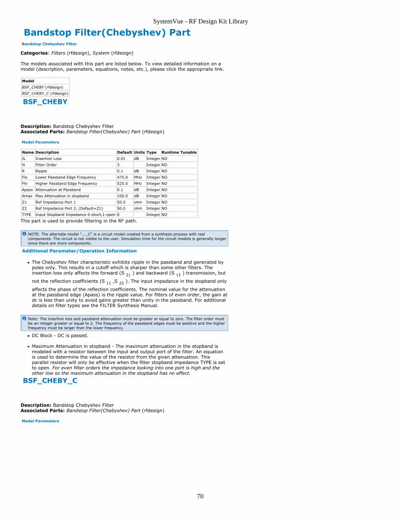
SystemVue - RF Design Kit Library
70
Bandstop Filter(Chebyshev) Part Bandstop Chebyshev Filter
Categories: Filters (rfdesign), System (rfdesign)
The models associated with this part are listed below. To view detailed information on amodel (description, parameters, equations, notes, etc.), please click the appropriate link.
Model
BSF_CHEBY (rfdesign)
BSF_CHEBY_C (rfdesign)
BSF_CHEBY
Description: Bandstop Chebyshev FilterAssociated Parts: Bandstop Filter(Chebyshev) Part (rfdesign)
Model Parameters
Name Description Default Units Type Runtime Tunable
IL Insertion Loss 0.01 dB Integer NO
N Filter Order 3 Integer NO
R Ripple 0.1 dB Integer NO
Flo Lower Passband Edge Frequency 475.0 MHz Integer NO
Fhi Higher Passband Edge Frequency 525.0 MHz Integer NO
Apass Attenuation at Passband 0.1 dB Integer NO
Amax Max Attenuation in stopband 100.0 dB Integer NO
Z1 Ref Impedance Port 1 50.0 ohm Integer NO
Z2 Ref Impedance Port 2, (Default=Z1) 50.0 ohm Integer NO
TYPE Input Stopband Impedance 0-short,1-open 0 Integer NO
This part is used to provide filtering in the RF path.
NOTE: The alternate model "..._C" is a circuit model created from a synthesis process with realcomponents. The circuit is not visible to the user. Simulation time for the circuit models is generally longersince there are more components.
Additional Parameter/Operation Information
The Chebyshev filter characteristic exhibits ripple in the passband and generated bypoles only. This results in a cutoff which is sharper than some other filters. Theinsertion loss only affects the forward (S 21 ) and backward (S 12 ) transmission, but
not the reflection coefficients (S 11 ,S 22 ). The input impedance in the stopband only
affects the phase of the reflection coefficients. The nominal value for the attenuationat the passband edge (Apass) is the ripple value. For filters of even order, the gain atdc is less than unity to avoid gains greater than unity in the passband. For additionaldetails on filter types see the FILTER Synthesis Manual.
Note: The insertion loss and passband attenuation must be greater or equal to zero. The filter order mustbe an integer greater or equal to 2. The frequency of the passband edges must be positive and the higherfrequency must be larger than the lower frequency.
DC Block - DC is passed.
Maximum Attenuation in stopband - The maximum attenuation in the stopband ismodeled with a resistor between the input and output port of the filter. An equationis used to determine the value of the resistor from the given attenuation. Thisparallel resistor will only be effective when the filter stopband impedance TYPE is setto open. For even filter orders the impedance looking into one port is high and theother low so the maximum attenuation in the stopband has no effect.
BSF_CHEBY_C
Description: Bandstop Chebyshev FilterAssociated Parts: Bandstop Filter(Chebyshev) Part (rfdesign)
Model Parameters

SystemVue - RF Design Kit Library
71
Name Description Default Units Type Runtime Tunable
IL Insertion Loss 0.01 dB Integer NO
N Filter Order 3 Integer NO
R Ripple 0.1 dB Integer NO
Flo Lower Passband Edge Frequency 475.0 MHz Integer NO
Fhi Higher Passband Edge Frequency 525.0 MHz Integer NO
Apass Attenuation at Passband 0.1 dB Integer NO
Amax Max Attenuation in stopband 100.0 dB Integer NO
Z1 Ref Impedance Port 1 50.0 ohm Integer NO
Z2 Ref Impedance Port 2, (Default=Z1) 50.0 ohm Integer NO
TYPE Input Stopband Impedance 0-short,1-open 0 Integer NO

SystemVue - RF Design Kit Library
72
Bandstop Filter(Elliptic) Part Bandstop Elliptic Filter
Categories: Filters (rfdesign), System (rfdesign)
The models associated with this part are listed below. To view detailed information on amodel (description, parameters, equations, notes, etc.), please click the appropriate link.
Model
BSF_ELLIPTIC (rfdesign)
BSF_ELLIPTIC_C (rfdesign)
BSF_ELLIPTIC
Description: Bandstop Elliptic FilterAssociated Parts: Bandstop Filter(Elliptic) Part (rfdesign)
Model Parameters
Name Description Default Units Type Runtime Tunable
IL Insertion Loss 0.01 dB Integer NO
N Filter Order 3 Integer NO
R Ripple 0.1 dB Integer NO
SBATTN Stopband Attenuation 40.0 dB Integer NO
Flo Lower Passband Edge Frequency 475.0 MHz Integer NO
Fhi Higher Passband Edge Frequency 525.0 MHz Integer NO
Amax Max Attenuation in stopband 100.0 dB Integer NO
Z1 Ref Impedance Port 1 50.0 ohm Integer NO
Z2 Ref Impedance Port 2, (Default=Z1) 50.0 ohm Integer NO
TYPE Input Stopband Impedance 0-short,1-open 0 Integer NO
This part is used to provide filtering in the RF path.
NOTE: The alternate model "..._C" is a circuit model created from a synthesis process with realcomponents. The circuit is not visible to the user. Simulation time for the circuit models is generally longersince there are more components.
Additional Parameter/Operation Information
The Elliptic filter characteristic exhibits ripple in the passband and generated by polesand zeros. This results in a cutoff which is sharper than most other filters. Theinsertion loss only affects the forward (S 21 ) and backward (S 12 ) transmission, but
not the reflection coefficients (S 11 ,S 22 ). The input impedance in the stopband only
affects the phase of the reflection coefficients. The value for the attenuation at thepassband edge (Apass) is the ripple value. For filters of even order, the gain at dc isless than unity to avoid gains greater than unity in the passband. For additionaldetails on filter types see the FILTER Synthesis Manual.
Note: The insertion loss must be greater or equal to zero. The filter order must be an integer greater orequal to 2. The frequencies of the passband edges must be positive and the higher frequency must belarger than the lower frequency. The stopband attenuation must be greater than the ripple.
DC Block - DC is passed.
Maximum Attenuation in stopband - The maximum attenuation in the stopband ismodeled with a resistor between the input and output port of the filter. An equationis used to determine the value of the resistor from the given attenuation. Thisparallel resistor will only be effective when the filter stopband impedance TYPE is setto open. For even filter orders the impedance looking into one port is high and theother low so the maximum attenuation in the stopband has no effect.
BSF_ELLIPTIC_C
Description: Bandstop Elliptic FilterAssociated Parts: Bandstop Filter(Elliptic) Part (rfdesign)
Model Parameters

SystemVue - RF Design Kit Library
73
Name Description Default Units Type Runtime Tunable
IL Insertion Loss 0.01 dB Integer NO
N Filter Order 3 Integer NO
R Ripple 0.1 dB Integer NO
SBATTN Stopband Attenuation 40.0 dB Integer NO
Flo Lower Passband Edge Frequency 475.0 MHz Integer NO
Fhi Higher Passband Edge Frequency 525.0 MHz Integer NO
Amax Max Attenuation in stopband 100.0 dB Integer NO
Z1 Ref Impedance Port 1 50.0 ohm Integer NO
Z2 Ref Impedance Port 2, (Default=Z1) 50.0 ohm Integer NO
TYPE Input Stopband Impedance 0-short,1-open 0 Integer NO

SystemVue - RF Design Kit Library
74
Bandstop Filter(Pole Zero) Part Bandstop Pole Zero Filter
Categories: Filters (rfdesign), System (rfdesign)
The models associated with this part are listed below. To view detailed information on amodel (description, parameters, equations, notes, etc.), please click the appropriate link.
Model
BSF_POLEZERO (rfdesign)
BSF_POLEZERO
Description: Bandstop Pole Zero FilterAssociated Parts: Bandstop Filter(Pole Zero) Part (rfdesign)
Model Parameters
Name Description Default Units Type RuntimeTunable
IL Insertion Loss 0.01 dB Integer NO
Flo Lower Passband Edge Frequency 475.0 MHz Integer NO
Fhi Higher Passband Edge Frequency 525.0 MHz Integer NO
Poles List of Poles [complex(-1,0);complex(-1,0)]
Text NO
Zeros List of Zeros [complex(-1,0)] Text NO
GainFactor Gain Factor 1 Float NO
Amax Max Attenuation in stopband 100.0 dB Integer NO
Z1 Ref Impedance Port 1 50.0 ohm Integer NO
Z2 Ref Impedance Port 2, (Default=Z1) 50.0 ohm Integer NO
TYPE Input Stopband Impedance 0-short,1-open
1 Integer NO
This part is used to provide filtering in the RF path.
Additional Parameter Information
Poles Poles are specified as a complex list separated by commas. For example, complex(a,b);complex(c,d)... Roots are normalized with respect to the frequency of the passband edge in rad/sec.
Zeros Zeros are specified as a complex list separated by commas. For example, complex(e,f);complex(g,h)... Roots are normalized with respect to the frequency of the passband edge inrad/sec.
GainFactor
If gain is greater than unity (non-passive network) at any frequency, the gain of the entire filter isreduced until the maximum gain is unity.
Additional Operation Information
Transfer Function:The filter transfer function for the low frequency prototype is of the form: G (s) = Gain Factor * { [ s-complex (e,f)] [s-complex(g,h)] } / { [s-complex(a,b)][s-complex(c,d)] }
The generalized pole/zero filter characteristic completely defined by the user. Thespecified poles and zeros define the low frequency prototype for the filter.Transformations are used as necessary for highpass, bandpass, and bandstopvariants. The insertion loss only affects the forward (S 21 ) and backward (S 12 )
transmission, but not the reflection coefficients (S 11 ,S 22 ). The input impedance in
the stopband only affects the phase of the reflection coefficients.
Note: The insertion loss and maximum stopband attenuation must be greater or equal to zero. Thefrequencies of the passband edges must be positive and the higher frequency must be larger than thelower frequency. The number of poles must be 1 or greater.
DC Block - DC is passed.
Maximum Attenuation in stopband - The maximum attenuation in the stopband ismodeled with a resistor between the input and output port of the filter. An equationis used to determine the value of the resistor from the given attenuation. Thisparallel resistor will only be effective when the filter stopband impedance TYPE is setto open.
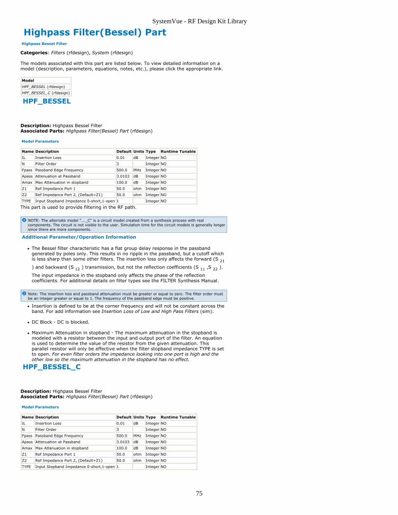
SystemVue - RF Design Kit Library
75
Highpass Filter(Bessel) Part Highpass Bessel Filter
Categories: Filters (rfdesign), System (rfdesign)
The models associated with this part are listed below. To view detailed information on amodel (description, parameters, equations, notes, etc.), please click the appropriate link.
Model
HPF_BESSEL (rfdesign)
HPF_BESSEL_C (rfdesign)
HPF_BESSEL
Description: Highpass Bessel FilterAssociated Parts: Highpass Filter(Bessel) Part (rfdesign)
Model Parameters
Name Description Default Units Type Runtime Tunable
IL Insertion Loss 0.01 dB Integer NO
N Filter Order 3 Integer NO
Fpass Passband Edge Frequency 500.0 MHz Integer NO
Apass Attenuation at Passband 3.0103 dB Integer NO
Amax Max Attenuation in stopband 100.0 dB Integer NO
Z1 Ref Impedance Port 1 50.0 ohm Integer NO
Z2 Ref Impedance Port 2, (Default=Z1) 50.0 ohm Integer NO
TYPE Input Stopband Impedance 0-short,1-open 1 Integer NO
This part is used to provide filtering in the RF path.
NOTE: The alternate model "..._C" is a circuit model created from a synthesis process with realcomponents. The circuit is not visible to the user. Simulation time for the circuit models is generally longersince there are more components.
Additional Parameter/Operation Information
The Bessel filter characteristic has a flat group delay response in the passbandgenerated by poles only. This results in no ripple in the passband, but a cutoff whichis less sharp than some other filters. The insertion loss only affects the forward (S 21
) and backward (S 12 ) transmission, but not the reflection coefficients (S 11 ,S 22 ).
The input impedance in the stopband only affects the phase of the reflectioncoefficients. For additional details on filter types see the FILTER Synthesis Manual.
Note: The insertion loss and passband attenuation must be greater or equal to zero. The filter order mustbe an integer greater or equal to 1. The frequency of the passband edge must be positive.
Insertion is defined to be at the corner frequency and will not be constant across theband. For add information see Insertion Loss of Low and High Pass Filters (sim).
DC Block - DC is blocked.
Maximum Attenuation in stopband - The maximum attenuation in the stopband ismodeled with a resistor between the input and output port of the filter. An equationis used to determine the value of the resistor from the given attenuation. Thisparallel resistor will only be effective when the filter stopband impedance TYPE is setto open. For even filter orders the impedance looking into one port is high and theother low so the maximum attenuation in the stopband has no effect.
HPF_BESSEL_C
Description: Highpass Bessel FilterAssociated Parts: Highpass Filter(Bessel) Part (rfdesign)
Model Parameters
Name Description Default Units Type Runtime Tunable
IL Insertion Loss 0.01 dB Integer NO
N Filter Order 3 Integer NO
Fpass Passband Edge Frequency 500.0 MHz Integer NO
Apass Attenuation at Passband 3.0103 dB Integer NO
Amax Max Attenuation in stopband 100.0 dB Integer NO
Z1 Ref Impedance Port 1 50.0 ohm Integer NO
Z2 Ref Impedance Port 2, (Default=Z1) 50.0 ohm Integer NO
TYPE Input Stopband Impedance 0-short,1-open 1 Integer NO

SystemVue - RF Design Kit Library
76
Highpass Filter(Butterworth) Part Highpass Butterworth Filter
Categories: Filters (rfdesign), System (rfdesign)
The models associated with this part are listed below. To view detailed information on amodel (description, parameters, equations, notes, etc.), please click the appropriate link.
Model
HPF_BUTTER (rfdesign)
HPF_BUTTER_C (rfdesign)
HPF_BUTTER
Description: Highpass Butterworth FilterAssociated Parts: Highpass Filter(Butterworth) Part (rfdesign)
Model Parameters
Name Description Default Units Type Runtime Tunable
IL Insertion Loss 0.01 dB Integer NO
N Filter Order 3 Integer NO
Fpass Passband Edge Frequency 500.0 MHz Integer NO
Apass Attenuation at Passband 3.0103 dB Integer NO
Amax Max Attenuation in stopband 100.0 dB Integer NO
Z1 Ref Impedance Port 1 50.0 ohm Integer NO
Z2 Ref Impedance Port 2, (Default=Z1) 50.0 ohm Integer NO
TYPE Input Stopband Impedance 0-short,1-open 1 Integer NO
This part is used to provide filtering in the RF path.
NOTE: The alternate model "..._C" is a circuit model created from a synthesis process with realcomponents. The circuit is not visible to the user. Simulation time for the circuit models is generally longersince there are more components.
Additional Parameter/Operation Information
The Butterworth filter characteristic is a maximally flat response in the passbandgenerated by poles only. This results in no ripple in the passband, but a cutoff whichis less sharp than some other filters. The insertion loss only affects the forward (S 21
) and backward (S 12 ) transmission, but not the reflection coefficients (S 11 ,S 22 ).
The input impedance in the stopband only affects the phase of the reflectioncoefficients. For additional details on filter types see the FILTER Synthesis Manual.
Note: The insertion loss and passband attenuation must be greater or equal to zero. The filter order mustbe an integer greater or equal to 1. The frequency of the passband edge must be positive.
Insertion is defined to be at the corner frequency and will not be constant across theband. For add information see Insertion Loss of Low and High Pass Filters (sim).
DC Block - DC is blocked.
Maximum Attenuation in stopband - The maximum attenuation in the stopband ismodeled with a resistor between the input and output port of the filter. An equationis used to determine the value of the resistor from the given attenuation. Thisparallel resistor will only be effective when the filter stopband impedance TYPE is setto open. For even filter orders the impedance looking into one port is high and theother low so the maximum attenuation in the stopband has no effect.
HPF_BUTTER_C
Description: Highpass Butterworth FilterAssociated Parts: Highpass Filter(Butterworth) Part (rfdesign)
Model Parameters
Name Description Default Units Type Runtime Tunable
IL Insertion Loss 0.01 dB Integer NO
N Filter Order 3 Integer NO
Fpass Passband Edge Frequency 500.0 MHz Integer NO
Apass Attenuation at Passband 3.0103 dB Integer NO
Amax Max Attenuation in stopband 100.0 dB Integer NO
Z1 Ref Impedance Port 1 50.0 ohm Integer NO
Z2 Ref Impedance Port 2, (Default=Z1) 50.0 ohm Integer NO
TYPE Input Stopband Impedance 0-short,1-open 1 Integer NO
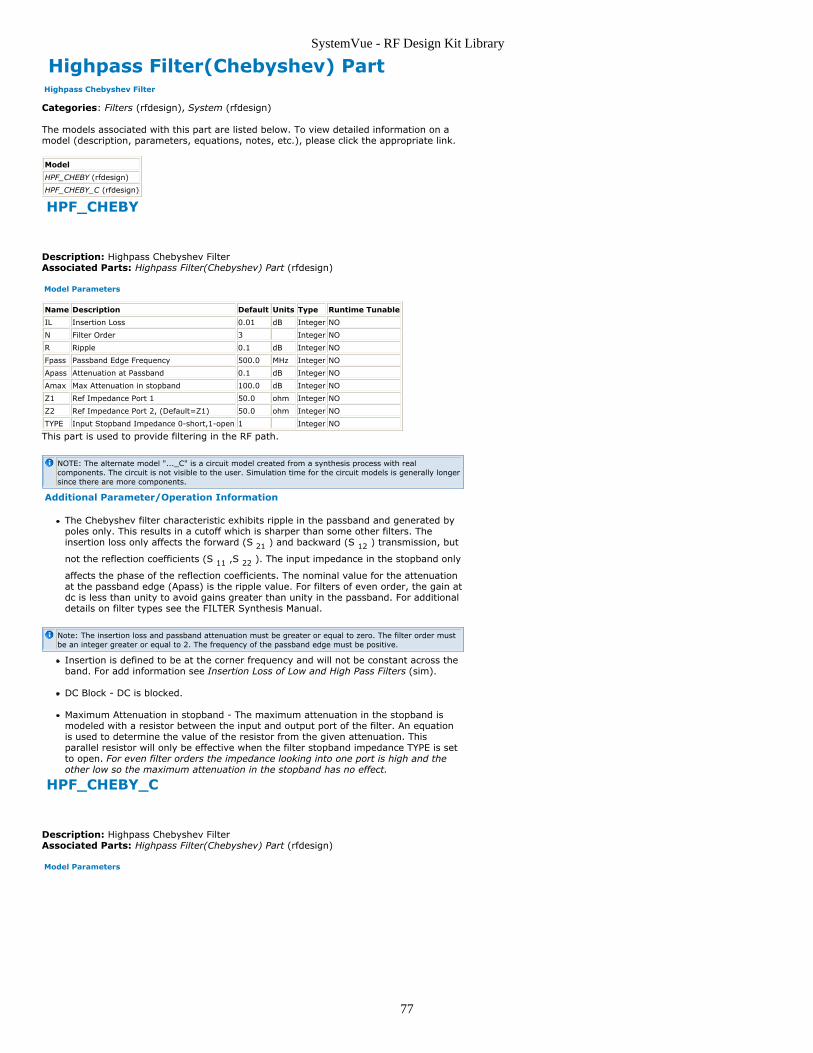
SystemVue - RF Design Kit Library
77
Highpass Filter(Chebyshev) Part Highpass Chebyshev Filter
Categories: Filters (rfdesign), System (rfdesign)
The models associated with this part are listed below. To view detailed information on amodel (description, parameters, equations, notes, etc.), please click the appropriate link.
Model
HPF_CHEBY (rfdesign)
HPF_CHEBY_C (rfdesign)
HPF_CHEBY
Description: Highpass Chebyshev FilterAssociated Parts: Highpass Filter(Chebyshev) Part (rfdesign)
Model Parameters
Name Description Default Units Type Runtime Tunable
IL Insertion Loss 0.01 dB Integer NO
N Filter Order 3 Integer NO
R Ripple 0.1 dB Integer NO
Fpass Passband Edge Frequency 500.0 MHz Integer NO
Apass Attenuation at Passband 0.1 dB Integer NO
Amax Max Attenuation in stopband 100.0 dB Integer NO
Z1 Ref Impedance Port 1 50.0 ohm Integer NO
Z2 Ref Impedance Port 2, (Default=Z1) 50.0 ohm Integer NO
TYPE Input Stopband Impedance 0-short,1-open 1 Integer NO
This part is used to provide filtering in the RF path.
NOTE: The alternate model "..._C" is a circuit model created from a synthesis process with realcomponents. The circuit is not visible to the user. Simulation time for the circuit models is generally longersince there are more components.
Additional Parameter/Operation Information
The Chebyshev filter characteristic exhibits ripple in the passband and generated bypoles only. This results in a cutoff which is sharper than some other filters. Theinsertion loss only affects the forward (S 21 ) and backward (S 12 ) transmission, but
not the reflection coefficients (S 11 ,S 22 ). The input impedance in the stopband only
affects the phase of the reflection coefficients. The nominal value for the attenuationat the passband edge (Apass) is the ripple value. For filters of even order, the gain atdc is less than unity to avoid gains greater than unity in the passband. For additionaldetails on filter types see the FILTER Synthesis Manual.
Note: The insertion loss and passband attenuation must be greater or equal to zero. The filter order mustbe an integer greater or equal to 2. The frequency of the passband edge must be positive.
Insertion is defined to be at the corner frequency and will not be constant across theband. For add information see Insertion Loss of Low and High Pass Filters (sim).
DC Block - DC is blocked.
Maximum Attenuation in stopband - The maximum attenuation in the stopband ismodeled with a resistor between the input and output port of the filter. An equationis used to determine the value of the resistor from the given attenuation. Thisparallel resistor will only be effective when the filter stopband impedance TYPE is setto open. For even filter orders the impedance looking into one port is high and theother low so the maximum attenuation in the stopband has no effect.
HPF_CHEBY_C
Description: Highpass Chebyshev FilterAssociated Parts: Highpass Filter(Chebyshev) Part (rfdesign)
Model Parameters

SystemVue - RF Design Kit Library
78
Name Description Default Units Type Runtime Tunable
IL Insertion Loss 0.01 dB Integer NO
N Filter Order 3 Integer NO
R Ripple 0.1 dB Integer NO
Fpass Passband Edge Frequency 500.0 MHz Integer NO
Apass Attenuation at Passband 0.1 dB Integer NO
Amax Max Attenuation in stopband 100.0 dB Integer NO
Z1 Ref Impedance Port 1 50.0 ohm Integer NO
Z2 Ref Impedance Port 2, (Default=Z1) 50.0 ohm Integer NO
TYPE Input Stopband Impedance 0-short,1-open 1 Integer NO
SystemVue - RF Design Kit Library
79
Highpass Filter(Elliptic) Part Highpass Elliptic Filter
Categories: Filters (rfdesign), System (rfdesign)
The models associated with this part are listed below. To view detailed information on amodel (description, parameters, equations, notes, etc.), please click the appropriate link.
Model
HPF_ELLIPTIC (rfdesign)
HPF_ELLIPTIC_C (rfdesign)
HPF_ELLIPTIC
Description: Highpass Elliptic FilterAssociated Parts: Highpass Filter(Elliptic) Part (rfdesign)
Model Parameters
Name Description Default Units Type Runtime Tunable
IL Insertion Loss 0.01 dB Integer NO
N Filter Order 3 Integer NO
R Ripple 0.1 dB Integer NO
SBATTN Stopband Attenuation 40.0 dB Integer NO
Fpass Passband Edge Frequency 500.0 MHz Integer NO
Amax Max Attenuation in stopband 100.0 dB Integer NO
Z1 Ref Impedance Port 1 50.0 ohm Integer NO
Z2 Ref Impedance Port 2, (Default=Z1) 50.0 ohm Integer NO
TYPE Input Stopband Impedance 0-short,1-open 1 Integer NO
This part is used to provide filtering in the RF path.
NOTE: The alternate model "..._C" is a circuit model created from a synthesis process with realcomponents. The circuit is not visible to the user. Simulation time for the circuit models is generally longersince there are more components.
Additional Parameter/Operation Information
The Elliptic filter characteristic exhibits ripple in the passband and generated by polesand zeros. This results in a cutoff which is sharper than most other filters. Theinsertion loss only affects the forward (S 21 ) and backward (S 12 ) transmission, but
not the reflection coefficients (S 11 ,S 22 ). The input impedance in the stopband only
affects the phase of the reflection coefficients. The value for the attenuation at thepassband edge (Apass) is the ripple value. For filters of even order, the gain at dc isless than unity to avoid gains greater than unity in the passband. For additionaldetails on filter types see the FILTER Synthesis Manual.
Note: The insertion loss must be greater or equal to zero. The filter order must be an integer greater orequal to 2. The frequency of the passband edge must be positive. The stopband attenuation must begreater than the ripple.
Insertion is defined to be at the corner frequency and will not be constant across theband. For add information see Insertion Loss of Low and High Pass Filters (sim).
DC Block - DC is blocked.
Maximum Attenuation in stopband - The maximum attenuation in the stopband ismodeled with a resistor between the input and output port of the filter. An equationis used to determine the value of the resistor from the given attenuation. Thisparallel resistor will only be effective when the filter stopband impedance TYPE is setto open. _For even filter orders the impedance looking into one port is high and theother low so the maximum attenuation in the stopband has no effect.
HPF_ELLIPTIC_C
Description: Highpass Elliptic FilterAssociated Parts: Highpass Filter(Elliptic) Part (rfdesign)
Model Parameters

SystemVue - RF Design Kit Library
80
Name Description Default Units Type Runtime Tunable
IL Insertion Loss 0.01 dB Integer NO
N Filter Order 3 Integer NO
R Ripple 0.1 dB Integer NO
SBATTN Stopband Attenuation 40.0 dB Integer NO
Fpass Passband Edge Frequency 500.0 MHz Integer NO
Amax Max Attenuation in stopband 100.0 dB Integer NO
Z1 Ref Impedance Port 1 50.0 ohm Integer NO
Z2 Ref Impedance Port 2, (Default=Z1) 50.0 ohm Integer NO
TYPE Input Stopband Impedance 0-short,1-open 1 Integer NO

SystemVue - RF Design Kit Library
81
Highpass Filter(Pole Zero) Part Highpass Pole Zero Filter
Categories: Filters (rfdesign), System (rfdesign)
The models associated with this part are listed below. To view detailed information on amodel (description, parameters, equations, notes, etc.), please click the appropriate link.
Model
HPF_POLEZERO (rfdesign)
HPF_POLEZERO
Description: Highpass Pole Zero FilterAssociated Parts: Highpass Filter(Pole Zero) Part (rfdesign)
Model Parameters
Name Description Default Units Type RuntimeTunable
IL Insertion Loss 0.01 dB Integer NO
Fpass Passband Edge Frequency 200.0 MHz Integer NO
Poles List of Poles [complex(-1,0);complex(-1,0)]
Text NO
Zeros List of Zeros [complex(-1,0)] Text NO
GainFactor Gain Factor 1 Float NO
Amax Max Attenuation in stopband 100.0 dB Integer NO
Z1 Ref Impedance Port 1 50.0 ohm Integer NO
Z2 Ref Impedance Port 2, (Default=Z1) 50.0 ohm Integer NO
TYPE Input Stopband Impedance 0-short,1-open
1 Integer NO
This part is used to provide filtering in the RF path.
Additional Parameter Information
Poles Poles are specified as a complex list separated by commas. For example, complex(a,b);complex(c,d)... Roots are normalized with respect to the frequency of the passband edge in rad/sec.
Zeros Zeros are specified as a complex list separated by commas. For example, complex(e,f);complex(g,h)... Roots are normalized with respect to the frequency of the passband edge inrad/sec.
GainFactor
If gain is greater than unity (non-passive network) at any frequency, the gain of the entire filter isreduced until the maximum gain is unity.
Additional Operation Information
Transfer Function:The filter transfer function for the low frequency prototype is of the form: G (s) = Gain Factor * { [ s-complex (e,f)] [s-complex(g,h)] } / { [s-complex(a,b)][s-complex(c,d)] }
The generalized pole/zero filter characteristic completely defined by the user. Thespecified poles and zeros define the low frequency prototype for the filter.Transformations are used as necessary for highpass, bandpass, and bandstopvariants. The insertion loss only affects the forward (S 21 ) and backward (S 12 )
transmission, but not the reflection coefficients (S 11 ,S 22 ). The input impedance in
the stopband only affects the phase of the reflection coefficients.
Note: The insertion loss and maximum stopband attenuation must be greater or equal to zero. Thefrequency of the passband edge must be positive. The number of poles must be 1 or greater.
DC Block - DC is blocked.
Maximum Attenuation in stopband - The maximum attenuation in the stopband ismodeled with a resistor between the input and output port of the filter. An equationis used to determine the value of the resistor from the given attenuation. Thisparallel resistor will only be effective when the filter stopband impedance TYPE is setto open.

SystemVue - RF Design Kit Library
82
Lowpass Filter(Bessel) Part Lowpass Bessel Filter
Categories: Filters (rfdesign), System (rfdesign)
The models associated with this part are listed below. To view detailed information on amodel (description, parameters, equations, notes, etc.), please click the appropriate link.
Model
LPF_BESSEL (rfdesign)
LPF_BESSEL_C (rfdesign)
LPF_BESSEL
Description: Lowpass Bessel FilterAssociated Parts: Lowpass Filter(Bessel) Part (rfdesign)
Model Parameters
Name Description Default Units Type Runtime Tunable
IL Insertion Loss 0.01 dB Integer NO
N Filter Order 3 Integer NO
Fpass Passband Edge Frequency 200.0 MHz Integer NO
Apass Attenuation at Passband 3.0103 dB Integer NO
Amax Max Attenuation in stopband 100.0 dB Integer NO
Z1 Ref Impedance Port 1 50.0 ohm Integer NO
Z2 Ref Impedance Port 2, (Default=Z1) 50.0 ohm Integer NO
TYPE Input Stopband Impedance 0-short,1-open 1 Integer NO
This part is used to provide filtering in the RF path.
NOTE: The alternate model "..._C" is a circuit model created from a synthesis process with realcomponents. The circuit is not visible to the user. Simulation time for the circuit models is generally longersince there are more components.
Additional Parameter/Operation Information
The Bessel filter characteristic has a flat group delay response in the passbandgenerated by poles only. This results in no ripple in the passband, but a cutoff whichis less sharp than some other filters. The insertion loss only affects the forward (S 21
) and backward (S 12 ) transmission, but not the reflection coefficients (S 11 ,S 22 ).
The input impedance in the stopband only affects the phase of the reflectioncoefficients. For additional details on filter types see the FILTER Synthesis Manual.
Note: The insertion loss and passband attenuation must be greater or equal to zero. The filter order mustbe an integer greater or equal to 1. The frequency of the passband edge must be positive.
Insertion is defined to be at the corner frequency and will not be constant across theband. For add information see Insertion Loss of Low and High Pass Filters (sim).
DC Block - DC is passed.
Maximum Attenuation in stopband - The maximum attenuation in the stopband ismodeled with a resistor between the input and output port of the filter. An equationis used to determine the value of the resistor from the given attenuation. Thisparallel resistor will only be effective when the filter stopband impedance TYPE is setto open. For even filter orders the impedance looking into one port is high and theother low so the maximum attenuation in the stopband has no effect.
LPF_BESSEL_C
Description: Lowpass Bessel FilterAssociated Parts: Lowpass Filter(Bessel) Part (rfdesign)
Model Parameters
Name Description Default Units Type Runtime Tunable
IL Insertion Loss 0.01 dB Integer NO
N Filter Order 3 Integer NO
Fpass Passband Edge Frequency 200.0 MHz Integer NO
Apass Attenuation at Passband 3.0103 dB Integer NO
Amax Max Attenuation in stopband 100.0 dB Integer NO
Z1 Ref Impedance Port 1 50.0 ohm Integer NO
Z2 Ref Impedance Port 2, (Default=Z1) 50.0 ohm Integer NO
TYPE Input Stopband Impedance 0-short,1-open 1 Integer NO

SystemVue - RF Design Kit Library
83
Lowpass Filter(Butterworth) Part Lowpass Butterworth Filter
Categories: Filters (rfdesign), System (rfdesign)
The models associated with this part are listed below. To view detailed information on amodel (description, parameters, equations, notes, etc.), please click the appropriate link.
Model
LPF_BUTTER (rfdesign)
LPF_BUTTER_C (rfdesign)
LPF_BUTTER
Description: Lowpass Butterworth FilterAssociated Parts: Lowpass Filter(Butterworth) Part (rfdesign)
Model Parameters
Name Description Default Units Type Runtime Tunable
IL Insertion Loss 0.01 dB Integer NO
N Filter Order 3 Integer NO
Fpass Passband Edge Frequency 200.0 MHz Integer NO
Apass Attenuation at Passband 3.0103 dB Integer NO
Amax Max Attenuation in stopband 100.0 dB Integer NO
Z1 Ref Impedance Port 1 50.0 ohm Integer NO
Z2 Ref Impedance Port 2, (Default=Z1) 50.0 ohm Integer NO
TYPE Input Stopband Impedance 0-short,1-open 1 Integer NO
This part is used to provide filtering in the RF path.
NOTE: The alternate model "..._C" is a circuit model created from a synthesis process with realcomponents. The circuit is not visible to the user. Simulation time for the circuit models is generally longersince there are more components.
Additional Parameter/Operation Information
The Butterworth filter characteristic is a maximally flat response in the passbandgenerated by poles only. This results in no ripple in the passband, but a cutoff whichis less sharp than some other filters. The insertion loss only affects the forward (S 21
) and backward (S 12 ) transmission, but not the reflection coefficients (S 11 ,S 22 ).
The input impedance in the stopband only affects the phase of the reflectioncoefficients. For additional details on filter types see the FILTER Synthesis section.
Note: The insertion loss and passband attenuation must be greater or equal to zero. The filter order mustbe an integer greater or equal to 1. The frequency of the passband edge must be positive.
Insertion is defined to be at the corner frequency and will not be constant across theband. For add information see Insertion Loss of Low and High Pass Filters (sim).
DC Block - DC is passed.
Maximum Attenuation in stopband - The maximum attenuation in the stopband ismodeled with a resistor between the input and output port of the filter. An equationis used to determine the value of the resistor from the given attenuation. Thisparallel resistor will only be effective when the filter stopband impedance TYPE is setto open. For even filter orders the impedance looking into one port is high and theother low so the maximum attenuation in the stopband has no effect.
LPF_BUTTER_C
Description: Lowpass Butterworth FilterAssociated Parts: Lowpass Filter(Butterworth) Part (rfdesign)
Model Parameters
Name Description Default Units Type Runtime Tunable
IL Insertion Loss 0.01 dB Integer NO
N Filter Order 3 Integer NO
Fpass Passband Edge Frequency 200.0 MHz Integer NO
Apass Attenuation at Passband 3.0103 dB Integer NO
Amax Max Attenuation in stopband 100.0 dB Integer NO
Z1 Ref Impedance Port 1 50.0 ohm Integer NO
Z2 Ref Impedance Port 2, (Default=Z1) 50.0 ohm Integer NO
TYPE Input Stopband Impedance 0-short,1-open 1 Integer NO

SystemVue - RF Design Kit Library
84
Lowpass Filter(Chebyshev) Part Lowpass Chebyshev Filter
Categories: Filters (rfdesign), System (rfdesign)
The models associated with this part are listed below. To view detailed information on amodel (description, parameters, equations, notes, etc.), please click the appropriate link.
Model
LPF_CHEBY (rfdesign)
LPF_CHEBY_C (rfdesign)
LPF_CHEBY
Description: Lowpass Chebyshev FilterAssociated Parts: Lowpass Filter(Chebyshev) Part (rfdesign)
Model Parameters
Name Description Default Units Type Runtime Tunable
IL Insertion Loss 0.01 dB Integer NO
N Filter Order 3 Integer NO
R Ripple 0.1 dB Integer NO
Fpass Passband Edge Frequency 200.0 MHz Integer NO
Apass Attenuation at Passband 0.1 dB Integer NO
Amax Max Attenuation in stopband 100.0 dB Integer NO
Z1 Ref Impedance Port 1 50.0 ohm Integer NO
Z2 Ref Impedance Port 2, (Default=Z1) 50.0 ohm Integer NO
TYPE Input Stopband Impedance 0-short,1-open 1 Integer NO
This part is used to provide filtering in the RF path.
NOTE: The alternate model "..._C" is a circuit model created from a synthesis process with realcomponents. The circuit is not visible to the user. Simulation time for the circuit models is generally longersince there are more components.
Additional Parameter/Operation Information
The Chebyshev filter characteristic exhibits ripple in the passband and generated bypoles only. This results in a cutoff which is sharper than some other filters. Theinsertion loss only affects the forward (S 21 ) and backward (S 12 ) transmission, but
not the reflection coefficients (S 11 ,S 22 ). The input impedance in the stopband only
affects the phase of the reflection coefficients. The nominal value for the attenuationat the passband edge (Apass) is the ripple value. For filters of even order, the gain atdc is less than unity to avoid gains greater than unity in the passband. For additionaldetails on filter types see the FILTER Synthesis Manual.
Note: The insertion loss and passband attenuation must be greater or equal to zero. The filter order mustbe an integer greater or equal to 2. The frequency of the passband edge must be positive.
Insertion is defined to be at the corner frequency and will not be constant across theband. For add information see Insertion Loss of Low and High Pass Filters (sim).
DC Block - DC is NOT blocked.
Maximum Attenuation in stopband - The maximum attenuation in the stopband ismodeled with a resistor between the input and output port of the filter. An equationis used to determine the value of the resistor from the given attenuation. Thisparallel resistor will only be effective when the filter stopband impedance TYPE is setto open. For even filter orders the impedance looking into one port is high and theother low so the maximum attenuation in the stopband has no effect.
LPF_CHEBY_C
Description: Lowpass Chebyshev FilterAssociated Parts: Lowpass Filter(Chebyshev) Part (rfdesign)
Model Parameters

SystemVue - RF Design Kit Library
85
Name Description Default Units Type Runtime Tunable
IL Insertion Loss 0.01 dB Integer NO
N Filter Order 3 Integer NO
R Ripple 0.1 dB Integer NO
Fpass Passband Edge Frequency 200.0 MHz Integer NO
Apass Attenuation at Passband 0.1 dB Integer NO
Amax Max Attenuation in stopband 100.0 dB Integer NO
Z1 Ref Impedance Port 1 50.0 ohm Integer NO
Z2 Ref Impedance Port 2, (Default=Z1) 50.0 ohm Integer NO
TYPE Input Stopband Impedance 0-short,1-open 1 Integer NO

SystemVue - RF Design Kit Library
86
Lowpass Filter(Elliptic) Part Lowpass Elliptic Filter
Categories: Filters (rfdesign), System (rfdesign)
The models associated with this part are listed below. To view detailed information on amodel (description, parameters, equations, notes, etc.), please click the appropriate link.
Model
LPF_ELLIPTIC (rfdesign)
LPF_ELLIPTIC_C (rfdesign)
LPF_ELLIPTIC
Description: Lowpass Elliptic FilterAssociated Parts: Lowpass Filter(Elliptic) Part (rfdesign)
Model Parameters
Name Description Default Units Type Runtime Tunable
IL Insertion Loss 0.01 dB Integer NO
N Filter Order 3 Integer NO
R Ripple 0.1 dB Integer NO
SBATTN Stopband Attenuation 40.0 dB Integer NO
Fpass Passband Edge Frequency 200.0 MHz Integer NO
Amax Max Attenuation in stopband 100.0 dB Integer NO
Z1 Ref Impedance Port 1 50.0 ohm Integer NO
Z2 Ref Impedance Port 2, (Default=Z1) 50.0 ohm Integer NO
TYPE Input Stopband Impedance 0-short,1-open 1 Integer NO
This part is used to provide filtering in the RF path.
NOTE: The alternate model "..._C" is a circuit model created from a synthesis process with realcomponents. The circuit is not visible to the user. Simulation time for the circuit models is generally longersince there are more components.
Additional Parameter/Operation Information
The Elliptic filter characteristic exhibits ripple in the passband and generated by polesand zeros. This results in a cutoff which is sharper than most other filters. Theinsertion loss only affects the forward (S 21 ) and backward (S 12 ) transmission, but
not the reflection coefficients (S 11 ,S 22 ). The input impedance in the stopband only
affects the phase of the reflection coefficients. The value for the attenuation at thepassband edge (Apass) is the ripple value. For filters of even order, the gain at dc isless than unity to avoid gains greater than unity in the passband. For additionaldetails on filter types see the FILTER Synthesis Manual.
Note: The insertion loss must be greater or equal to zero. The filter order must be an integer greater orequal to 2. The frequency of the passband edge must be positive. The stopband attenuation must begreater than the ripple.
Insertion is defined to be at the corner frequency and will not be constant across theband. For add information see Insertion Loss of Low and High Pass Filters (sim).
DC Block - DC is NOT blocked.
Maximum Attenuation in stopband - The maximum attenuation in the stopband ismodeled with a resistor between the input and output port of the filter. An equationis used to determine the value of the resistor from the given attenuation. Thisparallel resistor will only be effective when the filter stopband impedance TYPE is setto open. For even filter orders the impedance looking into one port is high and theother low so the maximum attenuation in the stopband has no effect.
LPF_ELLIPTIC_C
Description: Lowpass Elliptic FilterAssociated Parts: Lowpass Filter(Elliptic) Part (rfdesign)
Model Parameters

SystemVue - RF Design Kit Library
87
Name Description Default Units Type Runtime Tunable
IL Insertion Loss 0.01 dB Integer NO
N Filter Order 3 Integer NO
R Ripple 0.1 dB Integer NO
SBATTN Stopband Attenuation 40.0 dB Integer NO
Fpass Passband Edge Frequency 200.0 MHz Integer NO
Amax Max Attenuation in stopband 100.0 dB Integer NO
Z1 Ref Impedance Port 1 50.0 ohm Integer NO
Z2 Ref Impedance Port 2, (Default=Z1) 50.0 ohm Integer NO
TYPE Input Stopband Impedance 0-short,1-open 1 Integer NO

SystemVue - RF Design Kit Library
88
Lowpass Filter(Pole Zero) Part Lowpass Pole Zero Filter
Categories: Filters (rfdesign), System (rfdesign)
The models associated with this part are listed below. To view detailed information on amodel (description, parameters, equations, notes, etc.), please click the appropriate link.
Model
LPF_POLEZERO (rfdesign)
LPF_POLEZERO
Description: Lowpass Pole Zero FilterAssociated Parts: Lowpass Filter(Pole Zero) Part (rfdesign)
Model Parameters
Name Description Default Units Type RuntimeTunable
IL Insertion Loss 0.01 dB Integer NO
Fpass Passband Edge Frequency 200.0 MHz Integer NO
Poles List of Poles [complex(-1,0);complex(-1,0)]
Text NO
Zeros List of Zeros [complex(-1,0)] Text NO
GainFactor Gain Factor 1 Float NO
Amax Max Attenuation in stopband 100.0 dB Integer NO
Z1 Ref Impedance Port 1 50.0 ohm Integer NO
Z2 Ref Impedance Port 2, (Default=Z1) 50.0 ohm Integer NO
TYPE Input Stopband Impedance 0-short,1-open
1 Integer NO
This part is used to provide filtering in the RF path.
Additional Parameter Information
Poles Poles are specified as a complex list separated by commas. For example, complex(a,b);complex(c,d)... Roots are normalized with respect to the frequency of the passband edge in rad/sec.
Zeros Zeros are specified as a complex list separated by commas. For example, complex(e,f);complex(g,h)... Roots are normalized with respect to the frequency of the passband edge inrad/sec.
GainFactor
If gain is greater than unity (non-passive network) at any frequency, the gain of the entire filter isreduced until the maximum gain is unity.
Additional Operation Information
Transfer FunctionThe filter transfer function for the low frequency prototype is of the form:G (s) = Gain Factor * { [ s-complex (e,f)] [s-complex(g,h)] } / { [s-complex(a,b)][s-complex(c,d)] }
The generalized pole/zero filter characteristic completely defined by the user. Thespecified poles and zeros define the low frequency prototype for the filter.Transformations are used as necessary for highpass, bandpass, and bandstopvariants. The insertion loss only affects the forward (S 21 ) and backward (S 12 )
transmission, but not the reflection coefficients (S 11 ,S 22 ). The input impedance in
the stopband only affects the phase of the reflection coefficients.
Note: The insertion loss and maximum stopband attenuation must be greater or equal to zero. Thefrequency of the passband edge must be positive. The number of poles must be 1 or greater.
DC Block - DC is NOT blocked.
Maximum Attenuation in stopband - The maximum attenuation in the stopband ismodelled with a resistor between the input and output port of the filter. An equationis used to determine the value of the resistor from the given attenuation. Thisparallel resistor will only be effective when the filter stopband impedance TYPE is setto open.

SystemVue - RF Design Kit Library
89
Circulator Part Circulator
Categories: System (rfdesign)
The models associated with this part are listed below. To view detailed information on amodel (description, parameters, equations, notes, etc.), please click the appropriate link.
Model
CIRCULATOR (rfdesign)
CIRCULATOR
This part is used to provide directional control of signals in the RF path.
Description: CirculatorAssociated Parts: Circulator Part (rfdesign)
Model Parameters
Name Description Default Units Type Runtime Tunable
IL Insertion Loss 0.5 dB Integer NO
ISO Isolation 30 dB Integer NO
ZIN1 Port 1 Input Impedance 50 ohm None NO
ZIN2 Port 2 Input Impedance 50 ohm None NO
ZIN3 Port 3 Input Impedance 50 ohm None NO
Notes/Equations
Insertion Loss, and Isolation is assumed to be constant across frequency.1.
Note: As the isolation is reduced to the point that it begins to approach the insertion loss the totalinsertion loss will no longer be the value specified by the user.
DC is blocked between all ports.2.

SystemVue - RF Design Kit Library
90
Delay Part Ideal Time Delay Block (DELAY). Delays the signal for a certain amount of time.
Categories: Ideal (rfdesign), System (rfdesign)
The models associated with this part are listed below. To view detailed information on amodel (description, parameters, equations, notes, etc.), please click the appropriate link.
Model
DELAY (rfdesign)
DELAY
Description: Ideal Time Delay Block (DELAY). Delays the signal for a certain amount oftime.Associated Parts: Delay Part (rfdesign)
Model Parameters
Name Description Default Units Type Runtime Tunable
T Time Delay 1 ns Float NO
Z0 Reference Impedance 50 ohm Float NO
Notes and Equations
This part is used to provide a pure time delay in the RF path.Additional Parameter/Operation Information
The time delay must be greater or equal to zero. The time delay creates a linearphase shift as a function of frequency (f) of the form:S 21 = e -j 2 pi f T .
In the reverse direction, S 12 = S 21 . An alternate formulation (Model DELAY2) is available
where S12 is the complex conjugate of S 21. DELAY2 is available by choosing "Model"
on the DELAY dialog box. This brings up the "Change Model" option. Under "NewModel" select "DELAY2".
DC Block - DC is NOT blocked.

SystemVue - RF Design Kit Library
91
Phase Shift Part Ideal Phase Shift (PHASE)
Categories: Ideal (rfdesign), System (rfdesign)
The models associated with this part are listed below. To view detailed information on amodel (description, parameters, equations, notes, etc.), please click the appropriate link.
Model
PHASE (rfdesign)
PHASE
Description: Ideal Phase Shift (PHASE)Associated Parts: Phase Shift Part (rfdesign)
Model Parameters
Name Description Default Units Type Runtime Tunable
A Constant phase for frequency < F 0 deg None NO
S Phase slope in deg / octave 0 deg None NO
F Frequency at which slope starts 0 MHz None NO
Z0 Reference Impedance 50 ohm Integer NO
Notes and Equations
Additional Parameter/Operation InformationThis part is used to provide a phase lag in the RF path.
These parts can be cascaded to obtain arbitrary phase responses. The frequency (F)must be greater or equal to zero. The time delay creates a linear phase shift as afunction of frequency (f) of the form:
21 = e -j 2 pi f T .
In the reverse direction, S 12 = S 21 . An alternate formulation (PHASE2) is available where S12
is the complex conjugate of S 21. PHASE2 is available by choosing "Model" on the
PHASE dialog box. This brings up the "Change Model" option. Under "New Model"select "PHASE2". Use the same symbol.
DC Block - DC is NOT blocked.

SystemVue - RF Design Kit Library
92
Inductor Part This is an ideal inductor model
Categories: Ideal (rfdesign), Inductors (rfdesign), Lumped (rfdesign)
The models associated with this part are listed below. To view detailed information on amodel (description, parameters, equations, notes, etc.), please click the appropriate link.
Model
IND (rfdesign)
INDQ (rfdesign)
Inductor (IND)
Lumped inductance with optional Q. Like many common parts, a short version of thesymbol is available by holding the SHIFT key down while placing the part.
Note: Use the keyboard shortcut key "L" to place an inductor.
Description: This is an ideal inductor modelAssociated Parts: Inductor Part (rfdesign)
Model Parameters
Name Description Default Units Type Runtime Tunable
L Inductance 1 nH Integer NO
Additional Parameters
Inductance (nH) Specifies the value of the inductor in nanoHenries.Inductor Q (optional) Specifies the quality factor of the inductor, modeled as constantwith frequency. This parameter is not required, and defaults to 1 million if not specified.Q is modeled as constant with frequency. It can be specified higher or lower than thedefault value.

SystemVue - RF Design Kit Library
93
InductorQ Part Ideal inductor with Q
Categories: Ideal (rfdesign), Inductors (rfdesign), Lumped (rfdesign)
The models associated with this part are listed below. To view detailed information on amodel (description, parameters, equations, notes, etc.), please click the appropriate link.
Model
INDQ (rfdesign)
Inductor with Q (INDQ)
This element is implemented as a series inductor plus frequency dependent resistor.
Description: Ideal inductor with QAssociated Parts: Inductor Part (rfdesign), InductorQ Part (rfdesign)
Model Parameters
Name Description Default Units Type Runtime Tunable
L Inductance 1 nH Integer NO
QL Inductor Q 1000000 Integer NO
F Frequency for Q 300 MHz Float NO
MODE 1:Prop to Freq,2:Prop tosqrt(f),3:Constant
3 Positiveinteger
NO
RDC DC Resistance 0 ohm Integer NO
Additional Parameters
L Inductance in nanohenries.QL Quality factor (default=1e+6)F Frequency for Q value (MHz)
MODE Selects the frequency variation of Q:1 - Q proportional to frequency (f) (default)2 - Q proportional to sqrt (f)3 - Q constant4 - Identical to ADS Mode = sqrt(f) (for compatibility)
RDC Resistance at dc (default = 1e-6 ohm)

SystemVue - RF Design Kit Library
94
Dataset 1-Port (S Param) Part 1-Port Dataset (S-Parameter)
Categories: Linear (rfdesign)
The models associated with this part are listed below. To view detailed information on amodel (description, parameters, equations, notes, etc.), please click the appropriate link.
Model
NPOD1 (rfdesign)
ONE (rfdesign)
NPOD1This is a dataset model. Y-parameters are read from the dataset. Imported S-parametersautomatically create a dataset with Y-parameters. This model is used when the S-Parameter data is present on the workspace tree.This model supports n number of ports. For example a NPOD1 would be a 1 port S-parameter dataset, whereas a NPOD2 would be a 2 port.
Description: 1-Port Dataset (S-Parameter)Associated Parts: File 1-Port (S Param) Part (rfdesign), Dataset 1-Port (S Param) Part(rfdesign)
Model Parameters
Name Description Default Units Type Runtime Tunable
InterpDomain Interpolation Domain 0 Positiveinteger
NO
ExtrapMode Extrapolation Mode 0 Positiveinteger
NO
DCExtrapMode DC Extrapolation Mode 1 Positiveinteger
NO
MakePhysical Make Physical 0 Positiveinteger
NO
Ceiling Extrapolation Ceiling 100 dB Float NO
Floor Exrapolation Floor -100 dB Float NO
MaxFreq Cutoff Frequency 1E+94 MHz Integer NO
RolloffSlope Rolloff Slope indB/Decade
10 dB Integer NO
DSName Dataset Name none Text NO
Yvar Y Variable Name YP Text NO
Parameter Information
IterpDomain- Interpolation domain (default: Data based):Data Based - defined by S-data file fomat.Polar - S-data interpolation in polar coordinates.Polar DB - S-data in dB interpolation in polar coordinates.Rectangle - S-data interpolation in rectangle coordinates (Re(S), Im(S)).
ExtrapMode - defines extrapolation method (default:Constant):Constant - using closest data point in all extrapolation area.Interpolation - using interpolation domain method for extrapolation.
DCExtrapMode - defines DC extrapolation method (default:Magnitude):Magnitude - using magnitude of extrapolated to DC Y-matrix, keeping matrixelements signs of Re(Y) to make it physical.Real - using real part of extrapolated to DC Y-matrix.Image - using image part of extrapolated to DC Y-matrix, keeping matrixelements signs of Re(Y) to make it physical.
Make Physical- S-parameters that are physical represent real world devices. Non-physical S-parameters means that some of the S- parameter entries violated theconstraints required to make the device physical. Generally, this occurs when the S-parameters were not extracted correctly or the test / calibration setup of the VNAwas not done correctly. An example of non-physical S-parameters would be a passivedevice that exhibits gain instead of loss. When this parameter is set to YES the S-parameter entries will be changed by the model to ensure the rules of physicalnessare achieved. To learn more about physical S-parameters read Physical S-Parameters(users) in the Users Guide.Ceiling- extrapolation ceiling for S-parameters in dB (default 200dB).Floor - extrapolation floor for S-parameters in dB (default -200dB).MaxFreq - maximum frequency (cutoff frequency) at which S-data will be scaledwith RolloffSlope dB/decade (default: 1e10 Hz).RolloffSlope- rolloff slope in db/decade (default : 20 dB), positive value definesnegative slope.DSName - name of the dataset found in the workspace tree.Yvar - name of the Y-parameters variable in the dataset. Generally, this is called YP.
To learn more about S-parameters read S-parameters (users) in the Users Guide.
1-Port Data File (S-Parameter w/1-Term) [ONE]
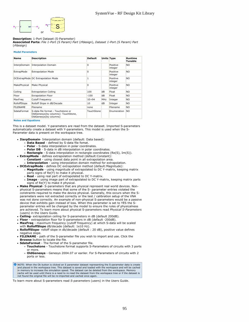
SystemVue - RF Design Kit Library
95
or
Description: 1-Port Dataset (S-Parameter)Associated Parts: File 1-Port (S Param) Part (rfdesign), Dataset 1-Port (S Param) Part(rfdesign)
Model Parameters
Name Description Default Units Type RuntimeTunable
InterpDomain Interpolation Domain 0 Positiveinteger
NO
ExtrapMode Extrapolation Mode 0 Positiveinteger
NO
DCExtrapMode DC Extrapolation Mode 1 Positiveinteger
NO
MakePhysical Make Physical 0 Positiveinteger
NO
Ceiling Extrapolation Ceiling 100 dB Float NO
Floor Exrapolation Floor -100 dB Float NO
MaxFreq Cutoff Frequency 1E+94 MHz Integer NO
RolloffSlope Rolloff Slope in dB/Decade 10 dB Integer NO
FILENAME Filename none Filename NO
SdataFormat S-data file format - Touchstone orOldGenesys(by columns): TouchStone,OldGenesys(by columns)
TouchStone Enumeration NO
Notes and Equations
This is a dataset model. Y-parameters are read from the dataset. Imported S-parametersautomatically create a dataset with Y-parameters. This model is used when the S-Parameter data is present on the workspace tree.
IterpDomain- Interpolation domain (default: Data based):Data Based - defined by S-data file fomat.Polar - S-data interpolation in polar coordinates.Polar DB - S-data in dB interpolation in polar coordinates.Rectangle - S-data interpolation in rectangle coordinates (Re(S), Im(S)).
ExtrapMode - defines extrapolation method (default:Constant):Constant - using closest data point in all extrapolation area.Interpolation - using interpolation domain method for extrapolation.
DCExtrapMode - defines DC extrapolation method (default:Magnitude):Magnitude - using magnitude of extrapolated to DC Y-matrix, keeping matrixparts signs of Re(Y) to make it physical.Real - using real part of extrapolated to DC Y-matrix.Image - using image part of extrapolated to DC Y-matrix, keeping matrix partssigns of Re(Y) to make it physical.
Make Physical- S-parameters that are physical represent real world devices. Non-physical S-parameters means that some of the S- parameter entries violated theconstraints required to make the device physical. Generally, this occurs when the S-parameters were not extracted correctly or the test / calibration setup of the VNAwas not done correctly. An example of non-physical S-parameters would be a passivedevice that exhibits gain instead of loss. When this parameter is set to YES the S-parameter entries will be changed by the model to ensure the rules of physicalnessare achieved. To learn more about physical S-parameters read Physical S-Parameters(users) in the Users Guide.Ceiling- extrapolation ceiling for S-parameters in dB (default 200dB).Floor - extrapolation floor for S-parameters in dB (default -200dB).MaxFreq - maximum frequency (cutoff frequency) at which S-data will be scaledwith RolloffSlope dB/decade (default: 1e10 Hz).RolloffSlope- rolloff slope in db/decade (default : 20 dB), positive value definesnegative slope.FILENAME - path of the S-parameter file you wish to import and use. Click theBrowse button to locate the file.SdataFormat - The format of the S-parameter file.
Touchstone - Touchstone format supports S-Parameters of circuits with 3 portsor more.OldGenesys - Genesys 2004.07 or eariler. For S-Parameters of circuits with 2ports or less.
NOTE: When the Ok button is clicked an S parameter dataset representing the S-parameter data is createand placed in the workspace tree. This dataset is saved and loaded with the workspace and will be cachedin memory to increase the simulation speed. The dataset can be deleted from the workspace. Memorycache will be used until there is a need to re-read the dataset from the workspace tree or if the dataset isnot found the original file will be re-imported and cached once again.
To learn more about S-parameters read S-parameters (users) in the Users Guide.

SystemVue - RF Design Kit Library
96
Dataset 2-Port (S Param) Part 2-Port Dataset (S-Parameter)
Categories: Linear (rfdesign)
The models associated with this part are listed below. To view detailed information on amodel (description, parameters, equations, notes, etc.), please click the appropriate link.
Model
NPOD2 (rfdesign)
TWO (rfdesign)
NPOD2This is a dataset model. Y-parameters are read from the dataset. Imported S-parametersautomatically create a dataset with Y-parameters. This model is used when the S-Parameter data is present on the workspace tree.This model supports n number of ports. For example a NPOD1 would be a 1 port S-parameter dataset, whereas a NPOD2 would be a 2 port.
Description: 2-Port Dataset (S-Parameter)Associated Parts: File 2-Port (S Param) Part (rfdesign), File 2-Port(S Param w block)Part (rfdesign), File 2-Port(Generic) Part (rfdesign), Dataset 2-Port (S Param) Part(rfdesign)
Model Parameters
Name Description Default Units Type Runtime Tunable
InterpDomain Interpolation Domain 0 Positiveinteger
NO
ExtrapMode Extrapolation Mode 0 Positiveinteger
NO
DCExtrapMode DC Extrapolation Mode 1 Positiveinteger
NO
MakePhysical Make Physical 0 Positiveinteger
NO
Ceiling Extrapolation Ceiling 100 dB Float NO
Floor Exrapolation Floor -100 dB Float NO
MaxFreq Cutoff Frequency 1E+94 MHz Integer NO
RolloffSlope Rolloff Slope indB/Decade
10 dB Integer NO
DSName Dataset Name none Text NO
Yvar Y Variable Name YP Text NO
Parameter Information
IterpDomain- Interpolation domain (default: Data based):Data Based - defined by S-data file fomat.Polar - S-data interpolation in polar coordinates.Polar DB - S-data in dB interpolation in polar coordinates.Rectangle - S-data interpolation in rectangle coordinates (Re(S), Im(S)).
ExtrapMode - defines extrapolation method (default:Constant):Constant - using closest data point in all extrapolation area.Interpolation - using interpolation domain method for extrapolation.
DCExtrapMode - defines DC extrapolation method (default:Magnitude):Magnitude - using magnitude of extrapolated to DC Y-matrix, keeping matrixelements signs of Re(Y) to make it physical.Real - using real part of extrapolated to DC Y-matrix.Image - using image part of extrapolated to DC Y-matrix, keeping matrixelements signs of Re(Y) to make it physical.
Make Physical- S-parameters that are physical represent real world devices. Non-physical S-parameters means that some of the S- parameter entries violated theconstraints required to make the device physical. Generally, this occurs when the S-parameters were not extracted correctly or the test / calibration setup of the VNAwas not done correctly. An example of non-physical S-parameters would be a passivedevice that exhibits gain instead of loss. When this parameter is set to YES the S-parameter entries will be changed by the model to ensure the rules of physicalnessare achieved. To learn more about physical S-parameters read Physical S-Parameters(users) in the Users Guide.Ceiling- extrapolation ceiling for S-parameters in dB (default 200dB).Floor - extrapolation floor for S-parameters in dB (default -200dB).MaxFreq - maximum frequency (cutoff frequency) at which S-data will be scaledwith RolloffSlope dB/decade (default: 1e10 Hz).RolloffSlope- rolloff slope in db/decade (default : 20 dB), positive value definesnegative slope.DSName - name of the dataset found in the workspace tree.Yvar - name of the Y-parameters variable in the dataset. Generally, this is called YP.
To learn more about S-parameters read S-parameters (users) in the Users Guide.
2-Port Data File (S-Parameter w/Generic) [TWO]

SystemVue - RF Design Kit Library
97
or
Description: 2-Port Dataset (S-Parameter)Associated Parts: File 2-Port (S Param) Part (rfdesign), File 2-Port(S Param w block)Part (rfdesign), File 2-Port(Generic) Part (rfdesign), Dataset 2-Port (S Param) Part(rfdesign)
Model Parameters
Name Description Default Units Type RuntimeTunable
InterpDomain Interpolation Domain 0 Positiveinteger
NO
ExtrapMode Extrapolation Mode 0 Positiveinteger
NO
DCExtrapMode DC Extrapolation Mode 1 Positiveinteger
NO
MakePhysical Make Physical 0 Positiveinteger
NO
Ceiling Extrapolation Ceiling 100 dB Float NO
Floor Exrapolation Floor -100 dB Float NO
MaxFreq Cutoff Frequency 1E+94 MHz Integer NO
RolloffSlope Rolloff Slope in dB/Decade 10 dB Integer NO
FILENAME Filename none Filename NO
SdataFormat S-data file format - Touchstone orOldGenesys(by columns): TouchStone,OldGenesys(by columns)
TouchStone Enumeration NO
This is a dataset model. Y-parameters are read from the dataset. Imported S-parametersautomatically create a dataset with Y-parameters. This model is used when the S-Parameter data is present on the workspace tree.
IterpDomain- Interpolation domain (default: Data based):1.Data Based - defined by S-data file fomat.2.Polar - S-data interpolation in polar coordinates.3.Polar DB - S-data in dB interpolation in polar coordinates.4.Rectangle - S-data interpolation in rectangle coordinates (Re(S), Im(S)).5.ExtrapMode - defines extrapolation method (default:Constant):6.Constant - using closest data point in all extrapolation area.7.Interpolation - using interpolation domain method for extrapolation.8.DCExtrapMode - defines DC extrapolation method (default:Magnitude):9.
Magnitude - using magnitude of extrapolated to DC Y-matrix, keeping matrixparts signs of Re(Y) to make it physical.Real - using real part of extrapolated to DC Y-matrix.Image - using image part of extrapolated to DC Y-matrix, keeping matrix partssigns of Re(Y) to make it physical.
Make Physical- S-parameters that are physical represent real world devices. Non-10.physical S-parameters means that some of the S- parameter entries violated theconstraints required to make the device physical. Generally, this occurs when the S-parameters were not extracted correctly or the test / calibration setup of the VNAwas not done correctly. An example of non-physical S-parameters would be a passivedevice that exhibits gain instead of loss. When this parameter is set to YES the S-parameter entries will be changed by the model to ensure the rules of physicalnessare achieved. To learn more about physical S-parameters read Physical S-Parameters(users) in the Users Guide.Ceiling- extrapolation ceiling for S-parameters in dB (default 200dB).11.Floor - extrapolation floor for S-parameters in dB (default -200dB).12.MaxFreq - maximum frequency (cutoff frequency) at which S-data will be scaled13.with RolloffSlope dB/decade (default: 1e10 Hz).RolloffSlope- rolloff slope in db/decade (default : 20 dB), positive value defines14.negative slope.FILENAME - path of the S-parameter file you wish to import and use. Click the15.Browse button to locate the file.SdataFormat - The format of the S-parameter file.16.Touchstone - Touchstone format supports S-Parameters of circuits with 3 ports or17.more.
NOTE: When the Ok button is clicked an S parameter dataset representing the S-parameter data is createand placed in the workspace tree. This dataset is saved and loaded with the workspace and will be cachedin memory to increase the simulation speed. The dataset can be deleted from the workspace. Memorycache will be used until there is a need to re-read the dataset from the workspace tree or if the dataset isnot found the original file will be re-imported and cached once again.
To learn more about S-parameters read S-parameters (users) in the Users Guide.

SystemVue - RF Design Kit Library
98
File 1-Port (S Param) Part 1-Port Data File (S-Parameter w/1-Term)
Categories: Linear (rfdesign)
The models associated with this part are listed below. To view detailed information on amodel (description, parameters, equations, notes, etc.), please click the appropriate link.
Model
ONE (rfdesign)
NPOD1 (rfdesign)

SystemVue - RF Design Kit Library
99
File 2-Port(Generic) Part 2-Port Data File (S-Parameter w/Generic)
Categories: Linear (rfdesign)
The models associated with this part are listed below. To view detailed information on amodel (description, parameters, equations, notes, etc.), please click the appropriate link.
Model
TWO (rfdesign)
NPOD2 (rfdesign)

SystemVue - RF Design Kit Library
100
File 2-Port (S Param) Part 2-Port Data File (S-Parameter w/2-Term)
Categories: Linear (rfdesign)
The models associated with this part are listed below. To view detailed information on amodel (description, parameters, equations, notes, etc.), please click the appropriate link.
Model
TWO (rfdesign)
NPOD2 (rfdesign)

SystemVue - RF Design Kit Library
101
File 2-Port(S Param w block) Part 2-Port Data File (S-Parameter w/BLOCK)
Categories: Linear (rfdesign)
The models associated with this part are listed below. To view detailed information on amodel (description, parameters, equations, notes, etc.), please click the appropriate link.
Model
TWO (rfdesign)
NPOD2 (rfdesign)

SystemVue - RF Design Kit Library
102
File 2-Port Split Gnd (S Param) Part 2-Port Data File Split Gnd (S-Parameter)
Categories: Linear (rfdesign)
The models associated with this part are listed below. To view detailed information on amodel (description, parameters, equations, notes, etc.), please click the appropriate link.
Model
TWO_SPLIT_GND (rfdesign)
TWO_SPLIT_GND
Description: 2-Port Data File Split Gnd (S-Parameter)Associated Parts: File 2-Port Split Gnd (S Param) Part (rfdesign)
Model Parameters
Name Description Default Units Type RuntimeTunable
FILENAME FileName none Filename NO
InterpDomain Interpolation domain (0:databased;1:polar;2:polar dB;3:rectangular): Databased, Polar, Polar dB, Rectangular
Databased
Enumeration NO
ExtrapMode Eaxtrapolation domain (0:const;1:interpolation):Constant, Interpolation
Constant Enumeration NO
DCExtrapMode DC Extrapolation mode(0:magnitude;1:real;2:image): Magnitude, Real,Image
Magnitude Enumeration NO
Ceiling Exatrapolation ceiling 100 dB Float NO
Floor Extrapolation floor -100 dB Float NO
MaxFreq Cutloff frequency 1E+94 MHz Float NO
RolloffSlope Rolloff slope in dB/dec 10 dB Float NO
MakePhysical Make data physical: NO, YES NO Enumeration NO
Notes and Equations
The TWO_SPLIT_GND is defined by 2-port S-Data and two grounds. This model isessentially a TWO model with the ground split between two pins. This is typically used formicrowave transistors that have a 2 ground package. These grounds can be connected toparts that simulate the package mounting effects such as via holes, resistances, orinductances. The linear simulator will add these grounding effects to the results of thespecified S-Data file.
Terminal 1 is the Input for the S-Data fileTerminal 2 is the Output for the S-Data fileTerminals 3 and 4 are grounds.
This is a dataset model. Y-parameters are read from the dataset. Imported S-parametersautomatically create a dataset with Y-parameters. This model is used when the S-Parameter data is present on the workspace tree.
IterpDomain- Interpolation domain (default: Data based):Data Based - defined by S-data file fomat.Polar - S-data interpolation in polar coordinates.Polar DB - S-data in dB interpolation in polar coordinates.Rectangle - S-data interpolation in rectangle coordinates (Re(S), Im(S)).
ExtrapMode - defines extrapolation method (default:Constant):Constant - using closest data point in all extrapolation area.Interpolation - using interpolation domain method for extrapolation.
DCExtrapMode - defines DC extrapolation method (default:Magnitude):Magnitude - using magnitude of extrapolated to DC Y-matrix, keeping matrixparts signs of Re(Y) to make it physical.Real - using real part of extrapolated to DC Y-matrix.Image - using image part of extrapolated to DC Y-matrix, keeping matrix partssigns of Re(Y) to make it physical.
Make Physical- S-parameters that are physical represent real world devices. Non-physical S-parameters means that some of the S- parameter entries violated theconstraints required to make the device physical. Generally, this occurs when the S-parameters were not extracted correctly or the test / calibration setup of the VNAwas not done correctly. An example of non-physical S-parameters would be a passivedevice that exhibits gain instead of loss. When this parameter is set to YES the S-parameter entries will be changed by the model to ensure the rules of physicalnessare achieved. To learn more about physical S-parameters read Physical S-Parameters(users) in the Users Guide.Ceiling- extrapolation ceiling for S-parameters in dB (default 200dB).Floor - extrapolation floor for S-parameters in dB (default -200dB).

SystemVue - RF Design Kit Library
103
MaxFreq - maximum frequency (cutoff frequency) at which S-data will be scaledwith RolloffSlope dB/decade (default: 1e10 Hz).RolloffSlope- rolloff slope in db/decade (default : 20 dB), positive value definesnegative slope.FILENAME - path of the S-parameter file you wish to import and use. Click theBrowse button to locate the file.
NOTE: When the Ok button is clicked an S parameter dataset representing the S-parameter data is createand placed in the workspace tree. This dataset is saved and loaded with the workspace and will be cachedin memory to increase the simulation speed. The dataset can be deleted from the workspace. Memorycache will be used until there is a need to re-read the dataset from the workspace tree or if the dataset isnot found the original file will be re-imported and cached once again.

SystemVue - RF Design Kit Library
104
File 3-Port (S Param) Part 3-Port Data File (S-Parameter)
Categories: Linear (rfdesign)
The models associated with this part are listed below. To view detailed information on amodel (description, parameters, equations, notes, etc.), please click the appropriate link.
Model
THR (rfdesign)
NPOD3 (rfdesign)
NPOD3Description: 3-Port Data File (S-Parameter)Associated Parts: File 3-Port (S Param) Part (rfdesign)
Model Parameters
Name Description Default Units Type Runtime Tunable
InterpDomain Interpolation Domain 0 Positiveinteger
NO
ExtrapMode Extrapolation Mode 0 Positiveinteger
NO
DCExtrapMode DC Extrapolation Mode 1 Positiveinteger
NO
MakePhysical Make Physical 0 Positiveinteger
NO
Ceiling Extrapolation Ceiling 100 dB Float NO
Floor Exrapolation Floor -100 dB Float NO
MaxFreq Cutoff Frequency 1E+94 MHz Integer NO
RolloffSlope Rolloff Slope indB/Decade
10 dB Integer NO
DSName Dataset Name none Text NO
Yvar Y Variable Name YP Text NO
Notes and Equations
This is a dataset model. Y-parameters are read from the dataset. Imported S-parametersautomatically create a dataset with Y-parameters. This model is used when the S-Parameter data is present on the workspace tree.
The NPOD model supports n number of ports. For example a NPOD1 would be a 1 port S-parameter dataset, whereas a NPOD2 would be a 2 port.
IterpDomain- Interpolation domain (default: Data based):Data Based - defined by S-data file fomat.Polar - S-data interpolation in polar coordinates.Polar DB - S-data in dB interpolation in polar coordinates.Rectangle - S-data interpolation in rectangle coordinates (Re(S), Im(S)).
ExtrapMode - defines extrapolation method (default:Constant):Constant - using closest data point in all extrapolation area.Interpolation - using interpolation domain method for extrapolation.
DCExtrapMode - defines DC extrapolation method (default:Magnitude):Magnitude - using magnitude of extrapolated to DC Y-matrix, keeping matrixparts signs of Re(Y) to make it physical.Real - using real part of extrapolated to DC Y-matrix.Image - using image part of extrapolated to DC Y-matrix, keeping matrix partssigns of Re(Y) to make it physical.
Make Physical- S-parameters that are physical represent real world devices. Non-physical S-parameters means that some of the S- parameter entries violated theconstraints required to make the device physical. Generally, this occurs when the S-parameters were not extracted correctly or the test / calibration setup of the VNAwas not done correctly. An example of non-physical S-parameters would be a passivedevice that exhibits gain instead of loss. When this parameter is set to YES the S-parameter entries will be changed by the model to ensure the rules of physicalnessare achieved. To learn more about physical S-parameters read Physical S-Parameters(users) in the Users Guide.Ceiling- extrapolation ceiling for S-parameters in dB (default 200dB).Floor - extrapolation floor for S-parameters in dB (default -200dB).MaxFreq - maximum frequency (cutoff frequency) at which S-data will be scaledwith RolloffSlope dB/decade (default: 1e10 Hz).RolloffSlope- rolloff slope in db/decade (default : 20 dB), positive value definesnegative slope.DSName - name of the dataset found in the workspace tree.Yvar - name of the Y-parameters variable in the dataset. Generally, this is called YP.
To learn more about S-parameters read S-parameters (users) in the Users Guide.
3-Port Data File (S-Parameter) [THR]

SystemVue - RF Design Kit Library
105
Description: 3-Port Data File (S-Parameter)Associated Parts: File 3-Port (S Param) Part (rfdesign)
Model Parameters
Name Description Default Units Type RuntimeTunable
InterpDomain Interpolation Domain 0 Positiveinteger
NO
ExtrapMode Extrapolation Mode 0 Positiveinteger
NO
DCExtrapMode DC Extrapolation Mode 1 Positiveinteger
NO
MakePhysical Make Physical 0 Positiveinteger
NO
Ceiling Extrapolation Ceiling 100 dB Float NO
Floor Exrapolation Floor -100 dB Float NO
MaxFreq Cutoff Frequency 1E+94 MHz Integer NO
RolloffSlope Rolloff Slope in dB/Decade 10 dB Integer NO
FILENAME Filename none Filename NO
SdataFormat S-data file format - Touchstone orOldGenesys(by columns): TouchStone,OldGenesys(by columns)
TouchStone Enumeration NO
Notes and Equations
This is a dataset model. Y-parameters are read from the dataset. Imported S-parametersautomatically create a dataset with Y-parameters. This model is used when the S-Parameter data is present on the workspace tree.
IterpDomain- Interpolation domain (default: Data based):Data Based - defined by S-data file fomat.Polar - S-data interpolation in polar coordinates.Polar DB - S-data in dB interpolation in polar coordinates.Rectangle - S-data interpolation in rectangle coordinates (Re(S), Im(S)).
ExtrapMode - defines extrapolation method (default:Constant):Constant - using closest data point in all extrapolation area.Interpolation - using interpolation domain method for extrapolation.
DCExtrapMode - defines DC extrapolation method (default:Magnitude):Magnitude - using magnitude of extrapolated to DC Y-matrix, keeping matrixparts signs of Re(Y) to make it physical.Real - using real part of extrapolated to DC Y-matrix.Image - using image part of extrapolated to DC Y-matrix, keeping matrix partssigns of Re(Y) to make it physical.
Make Physical- S-parameters that are physical represent real world devices. Non-physical S-parameters means that some of the S- parameter entries violated theconstraints required to make the device physical. Generally, this occurs when the S-parameters were not extracted correctly or the test / calibration setup of the VNAwas not done correctly. An example of non-physical S-parameters would be a passivedevice that exhibits gain instead of loss. When this parameter is set to YES the S-parameter entries will be changed by the model to ensure the rules of physicalnessare achieved. To learn more about physical S-parameters read Physical S-Parameters(users) in the Users Guide.Ceiling- extrapolation ceiling for S-parameters in dB (default 200dB).Floor - extrapolation floor for S-parameters in dB (default -200dB).MaxFreq - maximum frequency (cutoff frequency) at which S-data will be scaledwith RolloffSlope dB/decade (default: 1e10 Hz).RolloffSlope- rolloff slope in db/decade (default : 20 dB), positive value definesnegative slope.FILENAME - path of the S-parameter file you wish to import and use. Click theBrowse button to locate the file.SdataFormat - The format of the S-parameter file.
Touchstone - Touchstone format supports S-Parameters of circuits with 3 portsor more.
NOTE: When the Ok button is clicked an S parameter dataset representing the S-parameter data is createand placed in the workspace tree. This dataset is saved and loaded with the workspace and will be cachedin memory to increase the simulation speed. The dataset can be deleted from the workspace. Memorycache will be used until there is a need to re-read the dataset from the workspace tree or if the dataset isnot found the original file will be re-imported and cached once again.
To learn more about S-parameters read S-parameters (users) in the Users Guide.

SystemVue - RF Design Kit Library
106
File 4-Port (S Param) Part 4-Port Data File (S-Parameter)
Categories: Linear (rfdesign)
The models associated with this part are listed below. To view detailed information on amodel (description, parameters, equations, notes, etc.), please click the appropriate link.
Model
FOU (rfdesign)
NPOD4 (rfdesign)
4-Port Data File (S-Parameter) [FOU]
Description: 4-Port Data File (S-Parameter)Associated Parts: File 4-Port (S Param) Part (rfdesign)
Model Parameters
Name Description Default Units Type RuntimeTunable
InterpDomain Interpolation Domain 0 Positiveinteger
NO
ExtrapMode Extrapolation Mode 0 Positiveinteger
NO
DCExtrapMode DC Extrapolation Mode 1 Positiveinteger
NO
MakePhysical Make Physical 0 Positiveinteger
NO
Ceiling Extrapolation Ceiling 100 dB Float NO
Floor Exrapolation Floor -100 dB Float NO
MaxFreq Cutoff Frequency 1E+94 MHz Integer NO
RolloffSlope Rolloff Slope in dB/Decade 10 dB Integer NO
FILENAME Filename none Filename NO
SdataFormat S-data file format - Touchstone orOldGenesys(by columns): TouchStone,OldGenesys(by columns)
TouchStone Enumeration NO
Notes and Equations
This is a dataset model. Y-parameters are read from the dataset. Imported S-parametersautomatically create a dataset with Y-parameters. This model is used when the S-Parameter data is present on the workspace tree.
IterpDomain- Interpolation domain (default: Data based):Data Based - defined by S-data file fomat.Polar - S-data interpolation in polar coordinates.Polar DB - S-data in dB interpolation in polar coordinates.Rectangle - S-data interpolation in rectangle coordinates (Re(S), Im(S)).
ExtrapMode - defines extrapolation method (default:Constant):Constant - using closest data point in all extrapolation area.Interpolation - using interpolation domain method for extrapolation.
DCExtrapMode - defines DC extrapolation method (default:Magnitude):Magnitude - using magnitude of extrapolated to DC Y-matrix, keeping matrixparts signs of Re(Y) to make it physical.Real - using real part of extrapolated to DC Y-matrix.Image - using image part of extrapolated to DC Y-matrix, keeping matrix partssigns of Re(Y) to make it physical.
Make Physical- S-parameters that are physical represent real world devices. Non-physical S-parameters means that some of the S- parameter entries violated theconstraints required to make the device physical. Generally, this occurs when the S-parameters were not extracted correctly or the test / calibration setup of the VNAwas not done correctly. An example of non-physical S-parameters would be a passivedevice that exhibits gain instead of loss. When this parameter is set to YES the S-parameter entries will be changed by the model to ensure the rules of physicalnessare achieved. To learn more about physical S-parameters read Physical S-Parameters(users) in the Users Guide.Ceiling- extrapolation ceiling for S-parameters in dB (default 200dB).Floor - extrapolation floor for S-parameters in dB (default -200dB).MaxFreq - maximum frequency (cutoff frequency) at which S-data will be scaledwith RolloffSlope dB/decade (default: 1e10 Hz).RolloffSlope- rolloff slope in db/decade (default : 20 dB), positive value definesnegative slope.FILENAME - path of the S-parameter file you wish to import and use. Click theBrowse button to locate the file.SdataFormat - The format of the S-parameter file.
Touchstone - Touchstone format supports S-Parameters of circuits with 3 ports
SystemVue - RF Design Kit Library
107
or more.
NOTE: When the Ok button is clicked an S parameter dataset representing the S-parameter data is createand placed in the workspace tree. This dataset is saved and loaded with the workspace and will be cachedin memory to increase the simulation speed. The dataset can be deleted from the workspace. Memorycache will be used until there is a need to re-read the dataset from the workspace tree or if the dataset isnot found the original file will be re-imported and cached once again.
To learn more about S-parameters read S-parameters (users) in the Users Guide.
NPOD4Description: 4-Port Data File (S-Parameter)Associated Parts: File 4-Port (S Param) Part (rfdesign)
Model Parameters
Name Description Default Units Type Runtime Tunable
InterpDomain Interpolation Domain 0 Positiveinteger
NO
ExtrapMode Extrapolation Mode 0 Positiveinteger
NO
DCExtrapMode DC Extrapolation Mode 1 Positiveinteger
NO
MakePhysical Make Physical 0 Positiveinteger
NO
Ceiling Extrapolation Ceiling 100 dB Float NO
Floor Exrapolation Floor -100 dB Float NO
MaxFreq Cutoff Frequency 1E+94 MHz Integer NO
RolloffSlope Rolloff Slope indB/Decade
10 dB Integer NO
DSName Dataset Name none Text NO
Yvar Y Variable Name YP Text NO
Notes and Equations
This is a dataset model. Y-parameters are read from the dataset. Imported S-parametersautomatically create a dataset with Y-parameters. This model is used when the S-Parameter data is present on the workspace tree.
The NPOD model supports n number of ports. For example a NPOD1 would be a 1 port S-parameter dataset, whereas a NPOD2 would be a 2 port.
IterpDomain- Interpolation domain (default: Data based):Data Based - defined by S-data file fomat.Polar - S-data interpolation in polar coordinates.Polar DB - S-data in dB interpolation in polar coordinates.Rectangle - S-data interpolation in rectangle coordinates (Re(S), Im(S)).
ExtrapMode - defines extrapolation method (default:Constant):Constant - using closest data point in all extrapolation area.Interpolation - using interpolation domain method for extrapolation.
DCExtrapMode - defines DC extrapolation method (default:Magnitude):Magnitude - using magnitude of extrapolated to DC Y-matrix, keeping matrixparts signs of Re(Y) to make it physical.Real - using real part of extrapolated to DC Y-matrix.Image - using image part of extrapolated to DC Y-matrix, keeping matrix partssigns of Re(Y) to make it physical.
Make Physical- S-parameters that are physical represent real world devices. Non-physical S-parameters means that some of the S- parameter entries violated theconstraints required to make the device physical. Generally, this occurs when the S-parameters were not extracted correctly or the test / calibration setup of the VNAwas not done correctly. An example of non-physical S-parameters would be a passivedevice that exhibits gain instead of loss. When this parameter is set to YES the S-parameter entries will be changed by the model to ensure the rules of physicalnessare achieved. To learn more about physical S-parameters read Physical S-Parameters(users) in the Users Guide.Ceiling- extrapolation ceiling for S-parameters in dB (default 200dB).Floor - extrapolation floor for S-parameters in dB (default -200dB).MaxFreq - maximum frequency (cutoff frequency) at which S-data will be scaledwith RolloffSlope dB/decade (default: 1e10 Hz).RolloffSlope- rolloff slope in db/decade (default : 20 dB), positive value definesnegative slope.DSName - name of the dataset found in the workspace tree.Yvar - name of the Y-parameters variable in the dataset. Generally, this is called YP.
To learn more about S-parameters read S-parameters (users) in the Users Guide.

SystemVue - RF Design Kit Library
108
File 5-Port (S Param) Part 5-Port Data File (S-Parameter w/NPO5)
Categories: Linear (rfdesign)
The models associated with this part are listed below. To view detailed information on amodel (description, parameters, equations, notes, etc.), please click the appropriate link.
Model
NPO5 (rfdesign)
5-Port Data File (S-Parameter w/NPO5) [NPO5]
Description: 5-Port Data File (S-Parameter w/NPO5)Associated Parts: File 5-Port (S Param) Part (rfdesign)
Model Parameters
Name Description Default Units Type RuntimeTunable
InterpDomain Interpolation Domain 0 Positiveinteger
NO
ExtrapMode Extrapolation Mode 0 Positiveinteger
NO
DCExtrapMode DC Extrapolation Mode 1 Positiveinteger
NO
MakePhysical Make Physical 0 Positiveinteger
NO
Ceiling Extrapolation Ceiling 100 dB Float NO
Floor Exrapolation Floor -100 dB Float NO
MaxFreq Cutoff Frequency 1E+94 MHz Integer NO
RolloffSlope Rolloff Slope in dB/Decade 10 dB Integer NO
FILENAME Filename none Filename NO
SdataFormat S-data file format - Touchstone orOldGenesys(by columns): TouchStone,OldGenesys(by columns)
TouchStone Enumeration NO
Notes and Equations
This is a dataset model. Y-parameters are read from the dataset. Imported S-parametersautomatically create a dataset with Y-parameters. This model is used when the S-Parameter data is present on the workspace tree.
IterpDomain- Interpolation domain (default: Data based):Data Based - defined by S-data file fomat.Polar - S-data interpolation in polar coordinates.Polar DB - S-data in dB interpolation in polar coordinates.Rectangle - S-data interpolation in rectangle coordinates (Re(S), Im(S)).
ExtrapMode - defines extrapolation method (default:Constant):Constant - using closest data point in all extrapolation area.Interpolation - using interpolation domain method for extrapolation.
DCExtrapMode - defines DC extrapolation method (default:Magnitude):Magnitude - using magnitude of extrapolated to DC Y-matrix, keeping matrixparts signs of Re(Y) to make it physical.Real - using real part of extrapolated to DC Y-matrix.Image - using image part of extrapolated to DC Y-matrix, keeping matrix partssigns of Re(Y) to make it physical.
Make Physical- S-parameters that are physical represent real world devices. Non-physical S-parameters means that some of the S- parameter entries violated theconstraints required to make the device physical. Generally, this occurs when the S-parameters were not extracted correctly or the test / calibration setup of the VNAwas not done correctly. An example of non-physical S-parameters would be a passivedevice that exhibits gain instead of loss. When this parameter is set to YES the S-parameter entries will be changed by the model to ensure the rules of physicalnessare achieved. To learn more about physical S-parameters read Physical S-Parameters(users) in the Users Guide.Ceiling- extrapolation ceiling for S-parameters in dB (default 200dB).Floor - extrapolation floor for S-parameters in dB (default -200dB).MaxFreq - maximum frequency (cutoff frequency) at which S-data will be scaledwith RolloffSlope dB/decade (default: 1e10 Hz).RolloffSlope- rolloff slope in db/decade (default : 20 dB), positive value definesnegative slope.FILENAME - path of the S-parameter file you wish to import and use. Click theBrowse button to locate the file.SdataFormat - The format of the S-parameter file.
Touchstone - Touchstone format supports S-Parameters of circuits with 3 portsor more.

SystemVue - RF Design Kit Library
109
NOTE: When the Ok button is clicked an S parameter dataset representing the S-parameter data is createand placed in the workspace tree. This dataset is saved and loaded with the workspace and will be cachedin memory to increase the simulation speed. The dataset can be deleted from the workspace. Memorycache will be used until there is a need to re-read the dataset from the workspace tree or if the dataset isnot found the original file will be re-imported and cached once again.
To learn more about S-parameters read S-parameters (users) in the Users Guide.

SystemVue - RF Design Kit Library
110
File 6-Port (S Param) Part 6-Port Data File (S-Parameter w/NPO6)
Categories: Linear (rfdesign)
The models associated with this part are listed below. To view detailed information on amodel (description, parameters, equations, notes, etc.), please click the appropriate link.
Model
NPO6 (rfdesign)
6-Port Data File (S-Parameter w/NPO6) [NPO6]
Description: 6-Port Data File (S-Parameter w/NPO6)Associated Parts: File 6-Port (S Param) Part (rfdesign)
Model Parameters
Name Description Default Units Type RuntimeTunable
InterpDomain Interpolation Domain 0 Positiveinteger
NO
ExtrapMode Extrapolation Mode 0 Positiveinteger
NO
DCExtrapMode DC Extrapolation Mode 1 Positiveinteger
NO
MakePhysical Make Physical 0 Positiveinteger
NO
Ceiling Extrapolation Ceiling 100 dB Float NO
Floor Exrapolation Floor -100 dB Float NO
MaxFreq Cutoff Frequency 1E+94 MHz Integer NO
RolloffSlope Rolloff Slope in dB/Decade 10 dB Integer NO
FILENAME Filename none Filename NO
SdataFormat S-data file format - Touchstone orOldGenesys(by columns): TouchStone,OldGenesys(by columns)
TouchStone Enumeration NO
Notes and Equations
This is a dataset model. Y-parameters are read from the dataset. Imported S-parametersautomatically create a dataset with Y-parameters. This model is used when the S-Parameter data is present on the workspace tree.
IterpDomain- Interpolation domain (default: Data based):Data Based - defined by S-data file fomat.Polar - S-data interpolation in polar coordinates.Polar DB - S-data in dB interpolation in polar coordinates.Rectangle - S-data interpolation in rectangle coordinates (Re(S), Im(S)).
ExtrapMode - defines extrapolation method (default:Constant):Constant - using closest data point in all extrapolation area.Interpolation - using interpolation domain method for extrapolation.
DCExtrapMode - defines DC extrapolation method (default:Magnitude):Magnitude - using magnitude of extrapolated to DC Y-matrix, keeping matrixparts signs of Re(Y) to make it physical.Real - using real part of extrapolated to DC Y-matrix.Image - using image part of extrapolated to DC Y-matrix, keeping matrix partssigns of Re(Y) to make it physical.
Make Physical- S-parameters that are physical represent real world devices. Non-physical S-parameters means that some of the S- parameter entries violated theconstraints required to make the device physical. Generally, this occurs when the S-parameters were not extracted correctly or the test / calibration setup of the VNAwas not done correctly. An example of non-physical S-parameters would be a passivedevice that exhibits gain instead of loss. When this parameter is set to YES the S-parameter entries will be changed by the model to ensure the rules of physicalnessare achieved. To learn more about physical S-parameters read Physical S-Parameters(users) in the Users Guide.Ceiling- extrapolation ceiling for S-parameters in dB (default 200dB).Floor - extrapolation floor for S-parameters in dB (default -200dB).MaxFreq - maximum frequency (cutoff frequency) at which S-data will be scaledwith RolloffSlope dB/decade (default: 1e10 Hz).RolloffSlope- rolloff slope in db/decade (default : 20 dB), positive value definesnegative slope.FILENAME - path of the S-parameter file you wish to import and use. Click theBrowse button to locate the file.SdataFormat - The format of the S-parameter file.
Touchstone - Touchstone format supports S-Parameters of circuits with 3 portsor more.

SystemVue - RF Design Kit Library
111
NOTE: When the Ok button is clicked an S parameter dataset representing the S-parameter data is createand placed in the workspace tree. This dataset is saved and loaded with the workspace and will be cachedin memory to increase the simulation speed. The dataset can be deleted from the workspace. Memorycache will be used until there is a need to re-read the dataset from the workspace tree or if the dataset isnot found the original file will be re-imported and cached once again.
To learn more about S-parameters read S-parameters (users) in the Users Guide.

SystemVue - RF Design Kit Library
112
File 7-Port (S Param) Part 7-Port Data File (S-Parameter w/NPO7)
Categories: Linear (rfdesign)
The models associated with this part are listed below. To view detailed information on amodel (description, parameters, equations, notes, etc.), please click the appropriate link.
Model
NPO7 (rfdesign)
NPOD7 (rfdesign)
7-Port Data File (S-Parameter w/NPO7) [NPO7]
Description: 7-Port Data File (S-Parameter w/NPO7)Associated Parts: File 7-Port (S Param) Part (rfdesign)
Model Parameters
Name Description Default Units Type RuntimeTunable
InterpDomain Interpolation Domain 0 Positiveinteger
NO
ExtrapMode Extrapolation Mode 0 Positiveinteger
NO
DCExtrapMode DC Extrapolation Mode 1 Positiveinteger
NO
MakePhysical Make Physical 0 Positiveinteger
NO
Ceiling Extrapolation Ceiling 100 dB Float NO
Floor Exrapolation Floor -100 dB Float NO
MaxFreq Cutoff Frequency 1E+94 MHz Integer NO
RolloffSlope Rolloff Slope in dB/Decade 10 dB Integer NO
FILENAME Filename none Filename NO
SdataFormat S-data file format - Touchstone orOldGenesys(by columns): TouchStone,OldGenesys(by columns)
TouchStone Enumeration NO
Notes and Equations
This is a dataset model. Y-parameters are read from the dataset. Imported S-parametersautomatically create a dataset with Y-parameters. This model is used when the S-Parameter data is present on the workspace tree.
IterpDomain- Interpolation domain (default: Data based):Data Based - defined by S-data file fomat.Polar - S-data interpolation in polar coordinates.Polar DB - S-data in dB interpolation in polar coordinates.Rectangle - S-data interpolation in rectangle coordinates (Re(S), Im(S)).
ExtrapMode - defines extrapolation method (default:Constant):Constant - using closest data point in all extrapolation area.Interpolation - using interpolation domain method for extrapolation.
DCExtrapMode - defines DC extrapolation method (default:Magnitude):Magnitude - using magnitude of extrapolated to DC Y-matrix, keeping matrixparts signs of Re(Y) to make it physical.Real - using real part of extrapolated to DC Y-matrix.Image - using image part of extrapolated to DC Y-matrix, keeping matrix partssigns of Re(Y) to make it physical.
Make Physical- S-parameters that are physical represent real world devices. Non-physical S-parameters means that some of the S- parameter entries violated theconstraints required to make the device physical. Generally, this occurs when the S-parameters were not extracted correctly or the test / calibration setup of the VNAwas not done correctly. An example of non-physical S-parameters would be a passivedevice that exhibits gain instead of loss. When this parameter is set to YES the S-parameter entries will be changed by the model to ensure the rules of physicalnessare achieved. To learn more about physical S-parameters read Physical S-Parameters(users) in the Users Guide.Ceiling- extrapolation ceiling for S-parameters in dB (default 200dB).Floor - extrapolation floor for S-parameters in dB (default -200dB).MaxFreq - maximum frequency (cutoff frequency) at which S-data will be scaledwith RolloffSlope dB/decade (default: 1e10 Hz).RolloffSlope- rolloff slope in db/decade (default : 20 dB), positive value definesnegative slope.FILENAME - path of the S-parameter file you wish to import and use. Click theBrowse button to locate the file.SdataFormat - The format of the S-parameter file.
Touchstone - Touchstone format supports S-Parameters of circuits with 3 ports

SystemVue - RF Design Kit Library
113
or more.
NOTE: When the Ok button is clicked an S parameter dataset representing the S-parameter data is createand placed in the workspace tree. This dataset is saved and loaded with the workspace and will be cachedin memory to increase the simulation speed. The dataset can be deleted from the workspace. Memorycache will be used until there is a need to re-read the dataset from the workspace tree or if the dataset isnot found the original file will be re-imported and cached once again.
To learn more about S-parameters read S-parameters (users) in the Users Guide.
NPOD7Description: 7-Port Data File (S-Parameter w/NPO7)Associated Parts: File 7-Port (S Param) Part (rfdesign)
Model Parameters
Name Description Default Units Type Runtime Tunable
InterpDomain Interpolation Domain 0 Positiveinteger
NO
ExtrapMode Extrapolation Mode 0 Positiveinteger
NO
DCExtrapMode DC Extrapolation Mode 1 Positiveinteger
NO
MakePhysical Make Physical 0 Positiveinteger
NO
Ceiling Extrapolation Ceiling 100 dB Float NO
Floor Exrapolation Floor -100 dB Float NO
MaxFreq Cutoff Frequency 1E+94 MHz Integer NO
RolloffSlope Rolloff Slope indB/Decade
10 dB Integer NO
DSName Dataset Name none Text NO
Yvar Y Variable Name YP Text NO
Notes and Equations
This is a dataset model. Y-parameters are read from the dataset. Imported S-parametersautomatically create a dataset with Y-parameters. This model is used when the S-Parameter data is present on the workspace tree.
The NPOD model supports n number of ports. For example a NPOD1 would be a 1 port S-parameter dataset, whereas a NPOD2 would be a 2 port.
IterpDomain- Interpolation domain (default: Data based):Data Based - defined by S-data file fomat.Polar - S-data interpolation in polar coordinates.Polar DB - S-data in dB interpolation in polar coordinates.Rectangle - S-data interpolation in rectangle coordinates (Re(S), Im(S)).
ExtrapMode - defines extrapolation method (default:Constant):Constant - using closest data point in all extrapolation area.Interpolation - using interpolation domain method for extrapolation.
DCExtrapMode - defines DC extrapolation method (default:Magnitude):Magnitude - using magnitude of extrapolated to DC Y-matrix, keeping matrixparts signs of Re(Y) to make it physical.Real - using real part of extrapolated to DC Y-matrix.Image - using image part of extrapolated to DC Y-matrix, keeping matrix partssigns of Re(Y) to make it physical.
Make Physical- S-parameters that are physical represent real world devices. Non-physical S-parameters means that some of the S- parameter entries violated theconstraints required to make the device physical. Generally, this occurs when the S-parameters were not extracted correctly or the test / calibration setup of the VNAwas not done correctly. An example of non-physical S-parameters would be a passivedevice that exhibits gain instead of loss. When this parameter is set to YES the S-parameter entries will be changed by the model to ensure the rules of physicalnessare achieved. To learn more about physical S-parameters read Physical S-Parameters(users) in the Users Guide.Ceiling- extrapolation ceiling for S-parameters in dB (default 200dB).Floor - extrapolation floor for S-parameters in dB (default -200dB).MaxFreq - maximum frequency (cutoff frequency) at which S-data will be scaledwith RolloffSlope dB/decade (default: 1e10 Hz).RolloffSlope- rolloff slope in db/decade (default : 20 dB), positive value definesnegative slope.DSName - name of the dataset found in the workspace tree.Yvar - name of the Y-parameters variable in the dataset. Generally, this is called YP.
To learn more about S-parameters read S-parameters (users) in the Users Guide.

SystemVue - RF Design Kit Library
114
File 8-Port (S Param) Part 8-Port Data File (S-Parameter w/NPO8)
Categories: Linear (rfdesign)
The models associated with this part are listed below. To view detailed information on amodel (description, parameters, equations, notes, etc.), please click the appropriate link.
Model
NPO8 (rfdesign)
NPOD8 (rfdesign)
8-Port Data File (S-Parameter w/NPO8) [NPO8]
Description: 8-Port Data File (S-Parameter w/NPO8)Associated Parts: File 8-Port (S Param) Part (rfdesign)
Model Parameters
Name Description Default Units Type RuntimeTunable
InterpDomain Interpolation Domain 0 Positiveinteger
NO
ExtrapMode Extrapolation Mode 0 Positiveinteger
NO
DCExtrapMode DC Extrapolation Mode 1 Positiveinteger
NO
MakePhysical Make Physical 0 Positiveinteger
NO
Ceiling Extrapolation Ceiling 100 dB Float NO
Floor Exrapolation Floor -100 dB Float NO
MaxFreq Cutoff Frequency 1E+94 MHz Integer NO
RolloffSlope Rolloff Slope in dB/Decade 10 dB Integer NO
FILENAME Filename none Filename NO
SdataFormat S-data file format - Touchstone orOldGenesys(by columns): TouchStone,OldGenesys(by columns)
TouchStone Enumeration NO
Notes and Equations
This is a dataset model. Y-parameters are read from the dataset. Imported S-parametersautomatically create a dataset with Y-parameters. This model is used when the S-Parameter data is present on the workspace tree.
IterpDomain- Interpolation domain (default: Data based):Data Based - defined by S-data file fomat.Polar - S-data interpolation in polar coordinates.Polar DB - S-data in dB interpolation in polar coordinates.Rectangle - S-data interpolation in rectangle coordinates (Re(S), Im(S)).
ExtrapMode - defines extrapolation method (default:Constant):Constant - using closest data point in all extrapolation area.Interpolation - using interpolation domain method for extrapolation.
DCExtrapMode - defines DC extrapolation method (default:Magnitude):Magnitude - using magnitude of extrapolated to DC Y-matrix, keeping matrixparts signs of Re(Y) to make it physical.Real - using real part of extrapolated to DC Y-matrix.Image - using image part of extrapolated to DC Y-matrix, keeping matrix partssigns of Re(Y) to make it physical.
Make Physical- S-parameters that are physical represent real world devices. Non-physical S-parameters means that some of the S- parameter entries violated theconstraints required to make the device physical. Generally, this occurs when the S-parameters were not extracted correctly or the test / calibration setup of the VNAwas not done correctly. An example of non-physical S-parameters would be a passivedevice that exhibits gain instead of loss. When this parameter is set to YES the S-parameter entries will be changed by the model to ensure the rules of physicalnessare achieved. To learn more about physical S-parameters read Physical S-Parameters(users) in the Users Guide.Ceiling- extrapolation ceiling for S-parameters in dB (default 200dB).Floor - extrapolation floor for S-parameters in dB (default -200dB).MaxFreq - maximum frequency (cutoff frequency) at which S-data will be scaledwith RolloffSlope dB/decade (default: 1e10 Hz).RolloffSlope- rolloff slope in db/decade (default : 20 dB), positive value definesnegative slope.FILENAME - path of the S-parameter file you wish to import and use. Click theBrowse button to locate the file.SdataFormat - The format of the S-parameter file.
Touchstone - Touchstone format supports S-Parameters of circuits with 3 ports

SystemVue - RF Design Kit Library
115
or more.
NOTE: When the Ok button is clicked an S parameter dataset representing the S-parameter data is createand placed in the workspace tree. This dataset is saved and loaded with the workspace and will be cachedin memory to increase the simulation speed. The dataset can be deleted from the workspace. Memorycache will be used until there is a need to re-read the dataset from the workspace tree or if the dataset isnot found the original file will be re-imported and cached once again.
To learn more about S-parameters read S-parameters (users) in the Users Guide.
NPOD8Description: 8-Port Data File (S-Parameter w/NPO8)Associated Parts: File 8-Port (S Param) Part (rfdesign)
Model Parameters
Name Description Default Units Type Runtime Tunable
InterpDomain Interpolation Domain 0 Positiveinteger
NO
ExtrapMode Extrapolation Mode 0 Positiveinteger
NO
DCExtrapMode DC Extrapolation Mode 1 Positiveinteger
NO
MakePhysical Make Physical 0 Positiveinteger
NO
Ceiling Extrapolation Ceiling 100 dB Float NO
Floor Exrapolation Floor -100 dB Float NO
MaxFreq Cutoff Frequency 1E+94 MHz Integer NO
RolloffSlope Rolloff Slope indB/Decade
10 dB Integer NO
DSName Dataset Name none Text NO
Yvar Y Variable Name YP Text NO
Notes and Equations
This is a dataset model. Y-parameters are read from the dataset. Imported S-parametersautomatically create a dataset with Y-parameters. This model is used when the S-Parameter data is present on the workspace tree.
The NPOD model supports n number of ports. For example a NPOD1 would be a 1 port S-parameter dataset, whereas a NPOD2 would be a 2 port.
IterpDomain- Interpolation domain (default: Data based):Data Based - defined by S-data file fomat.Polar - S-data interpolation in polar coordinates.Polar DB - S-data in dB interpolation in polar coordinates.Rectangle - S-data interpolation in rectangle coordinates (Re(S), Im(S)).
ExtrapMode - defines extrapolation method (default:Constant):Constant - using closest data point in all extrapolation area.Interpolation - using interpolation domain method for extrapolation.
DCExtrapMode - defines DC extrapolation method (default:Magnitude):Magnitude - using magnitude of extrapolated to DC Y-matrix, keeping matrixparts signs of Re(Y) to make it physical.Real - using real part of extrapolated to DC Y-matrix.Image - using image part of extrapolated to DC Y-matrix, keeping matrix partssigns of Re(Y) to make it physical.
Make Physical- S-parameters that are physical represent real world devices. Non-physical S-parameters means that some of the S- parameter entries violated theconstraints required to make the device physical. Generally, this occurs when the S-parameters were not extracted correctly or the test / calibration setup of the VNAwas not done correctly. An example of non-physical S-parameters would be a passivedevice that exhibits gain instead of loss. When this parameter is set to YES the S-parameter entries will be changed by the model to ensure the rules of physicalnessare achieved. To learn more about physical S-parameters read Physical S-Parameters(users) in the Users Guide.Ceiling- extrapolation ceiling for S-parameters in dB (default 200dB).Floor - extrapolation floor for S-parameters in dB (default -200dB).MaxFreq - maximum frequency (cutoff frequency) at which S-data will be scaledwith RolloffSlope dB/decade (default: 1e10 Hz).RolloffSlope- rolloff slope in db/decade (default : 20 dB), positive value definesnegative slope.DSName - name of the dataset found in the workspace tree.Yvar - name of the Y-parameters variable in the dataset. Generally, this is called YP.
To learn more about S-parameters read S-parameters (users) in the Users Guide.

SystemVue - RF Design Kit Library
116
File 9-Port (S Param) Part 9-Port Data File (S-Parameter w/NPO9)
Categories: Linear (rfdesign)
The models associated with this part are listed below. To view detailed information on amodel (description, parameters, equations, notes, etc.), please click the appropriate link.
Model
NPO9 (rfdesign)
NPOD9 (rfdesign)
9-Port Data File (S-Parameter w/NPO9) [NPO9]
Description: 9-Port Data File (S-Parameter w/NPO9)Associated Parts: File 9-Port (S Param) Part (rfdesign)
Model Parameters
Name Description Default Units Type RuntimeTunable
InterpDomain Interpolation Domain 0 Positiveinteger
NO
ExtrapMode Extrapolation Mode 0 Positiveinteger
NO
DCExtrapMode DC Extrapolation Mode 1 Positiveinteger
NO
MakePhysical Make Physical 0 Positiveinteger
NO
Ceiling Extrapolation Ceiling 100 dB Float NO
Floor Exrapolation Floor -100 dB Float NO
MaxFreq Cutoff Frequency 1E+94 MHz Integer NO
RolloffSlope Rolloff Slope in dB/Decade 10 dB Integer NO
FILENAME Filename none Filename NO
SdataFormat S-data file format - Touchstone orOldGenesys(by columns): TouchStone,OldGenesys(by columns)
TouchStone Enumeration NO
Notes and Equations
This is a dataset model. Y-parameters are read from the dataset. Imported S-parametersautomatically create a dataset with Y-parameters. This model is used when the S-Parameter data is present on the workspace tree.
IterpDomain- Interpolation domain (default: Data based):Data Based - defined by S-data file fomat.Polar - S-data interpolation in polar coordinates.Polar DB - S-data in dB interpolation in polar coordinates.Rectangle - S-data interpolation in rectangle coordinates (Re(S), Im(S)).
ExtrapMode - defines extrapolation method (default:Constant):Constant - using closest data point in all extrapolation area.Interpolation - using interpolation domain method for extrapolation.
DCExtrapMode - defines DC extrapolation method (default:Magnitude):Magnitude - using magnitude of extrapolated to DC Y-matrix, keeping matrixparts signs of Re(Y) to make it physical.Real - using real part of extrapolated to DC Y-matrix.Image - using image part of extrapolated to DC Y-matrix, keeping matrix partssigns of Re(Y) to make it physical.
Make Physical- S-parameters that are physical represent real world devices. Non-physical S-parameters means that some of the S- parameter entries violated theconstraints required to make the device physical. Generally, this occurs when the S-parameters were not extracted correctly or the test / calibration setup of the VNAwas not done correctly. An example of non-physical S-parameters would be a passivedevice that exhibits gain instead of loss. When this parameter is set to YES the S-parameter entries will be changed by the model to ensure the rules of physicalnessare achieved. To learn more about physical S-parameters read Physical S-Parameters(users) in the Users Guide.Ceiling- extrapolation ceiling for S-parameters in dB (default 200dB).Floor - extrapolation floor for S-parameters in dB (default -200dB).MaxFreq - maximum frequency (cutoff frequency) at which S-data will be scaledwith RolloffSlope dB/decade (default: 1e10 Hz).RolloffSlope- rolloff slope in db/decade (default : 20 dB), positive value definesnegative slope.FILENAME - path of the S-parameter file you wish to import and use. Click theBrowse button to locate the file.

SystemVue - RF Design Kit Library
117
SdataFormat - The format of the S-parameter file.Touchstone - Touchstone format supports S-Parameters of circuits with 3 portsor more.
NOTE: When the Ok button is clicked an S parameter dataset representing the S-parameter data is createand placed in the workspace tree. This dataset is saved and loaded with the workspace and will be cachedin memory to increase the simulation speed. The dataset can be deleted from the workspace. Memorycache will be used until there is a need to re-read the dataset from the workspace tree or if the dataset isnot found the original file will be re-imported and cached once again.
To learn more about S-parameters read S-parameters (users) in the Users Guide.
NPOD9Description: 9-Port Data File (S-Parameter w/NPO9)Associated Parts: File 9-Port (S Param) Part (rfdesign)
Model Parameters
Name Description Default Units Type Runtime Tunable
InterpDomain Interpolation Domain 0 Positiveinteger
NO
ExtrapMode Extrapolation Mode 0 Positiveinteger
NO
DCExtrapMode DC Extrapolation Mode 1 Positiveinteger
NO
MakePhysical Make Physical 0 Positiveinteger
NO
Ceiling Extrapolation Ceiling 100 dB Float NO
Floor Exrapolation Floor -100 dB Float NO
MaxFreq Cutoff Frequency 1E+94 MHz Integer NO
RolloffSlope Rolloff Slope indB/Decade
10 dB Integer NO
DSName Dataset Name none Text NO
Yvar Y Variable Name YP Text NO
Notes and Equations
This is a dataset model. Y-parameters are read from the dataset. Imported S-parametersautomatically create a dataset with Y-parameters. This model is used when the S-Parameter data is present on the workspace tree.
The NPOD model supports n number of ports. For example a NPOD1 would be a 1 port S-parameter dataset, whereas a NPOD2 would be a 2 port.
IterpDomain- Interpolation domain (default: Data based):Data Based - defined by S-data file fomat.Polar - S-data interpolation in polar coordinates.Polar DB - S-data in dB interpolation in polar coordinates.Rectangle - S-data interpolation in rectangle coordinates (Re(S), Im(S)).
ExtrapMode - defines extrapolation method (default:Constant):Constant - using closest data point in all extrapolation area.Interpolation - using interpolation domain method for extrapolation.
DCExtrapMode - defines DC extrapolation method (default:Magnitude):Magnitude - using magnitude of extrapolated to DC Y-matrix, keeping matrixparts signs of Re(Y) to make it physical.Real - using real part of extrapolated to DC Y-matrix.Image - using image part of extrapolated to DC Y-matrix, keeping matrix partssigns of Re(Y) to make it physical.
Make Physical- S-parameters that are physical represent real world devices. Non-physical S-parameters means that some of the S- parameter entries violated theconstraints required to make the device physical. Generally, this occurs when the S-parameters were not extracted correctly or the test / calibration setup of the VNAwas not done correctly. An example of non-physical S-parameters would be a passivedevice that exhibits gain instead of loss. When this parameter is set to YES the S-parameter entries will be changed by the model to ensure the rules of physicalnessare achieved. To learn more about physical S-parameters read Physical S-Parameters(users) in the Users Guide.Ceiling- extrapolation ceiling for S-parameters in dB (default 200dB).Floor - extrapolation floor for S-parameters in dB (default -200dB).MaxFreq - maximum frequency (cutoff frequency) at which S-data will be scaledwith RolloffSlope dB/decade (default: 1e10 Hz).RolloffSlope- rolloff slope in db/decade (default : 20 dB), positive value definesnegative slope.DSName - name of the dataset found in the workspace tree.Yvar - name of the Y-parameters variable in the dataset. Generally, this is called YP.
To learn more about S-parameters read S-parameters (users) in the Users Guide.

SystemVue - RF Design Kit Library
118
File 10-Port (S Param) Part 10-Port Data File (S-Parameter w/NPO10)
Categories: Linear (rfdesign)
The models associated with this part are listed below. To view detailed information on amodel (description, parameters, equations, notes, etc.), please click the appropriate link.
Model
NPO10 (rfdesign)
NPOD10 (rfdesign)
N-port Data File (S-Parameter w/NPO_N) [NPO10]
Description: N-port Data File (S-Parameter w/NPO_N)Associated Parts: File 10-Port (S Param) Part (rfdesign), File N-Port (S Param) Part(rfdesign)
Model Parameters
Name Description Default Units Type RuntimeTunable
InterpDomain Interpolation Domain 0 Positiveinteger
NO
ExtrapMode Extrapolation Mode 0 Positiveinteger
NO
DCExtrapMode DC Extrapolation Mode 1 Positiveinteger
NO
MakePhysical Make Physical 0 Positiveinteger
NO
Ceiling Extrapolation Ceiling 100 dB Float NO
Floor Exrapolation Floor -100 dB Float NO
MaxFreq Cutoff Frequency 1E+94 MHz Integer NO
RolloffSlope Rolloff Slope in dB/Decade 10 dB Integer NO
FILENAME Filename none Filename NO
SdataFormat S-data file format - Touchstone orOldGenesys(by columns): TouchStone,OldGenesys(by columns)
TouchStone Enumeration NO
Notes and Equations
This is a dataset model. Y-parameters are read from the dataset. Imported S-parametersautomatically create a dataset with Y-parameters. This model is used when the S-Parameter data is present on the workspace tree.
The NPO model can be used for any number of points. Use the model NPOn where n isthe number of ports. A generic symbol with n number of points will be generated.
IterpDomain- Interpolation domain (default: Data based):Data Based - defined by S-data file fomat.Polar - S-data interpolation in polar coordinates.Polar DB - S-data in dB interpolation in polar coordinates.Rectangle - S-data interpolation in rectangle coordinates (Re(S), Im(S)).
ExtrapMode - defines extrapolation method (default:Constant):Constant - using closest data point in all extrapolation area.Interpolation - using interpolation domain method for extrapolation.
DCExtrapMode - defines DC extrapolation method (default:Magnitude):Magnitude - using magnitude of extrapolated to DC Y-matrix, keeping matrixparts signs of Re(Y) to make it physical.Real - using real part of extrapolated to DC Y-matrix.Image - using image part of extrapolated to DC Y-matrix, keeping matrix partssigns of Re(Y) to make it physical.
Make Physical- S-parameters that are physical represent real world devices. Non-physical S-parameters means that some of the S- parameter entries violated theconstraints required to make the device physical. Generally, this occurs when the S-parameters were not extracted correctly or the test / calibration setup of the VNAwas not done correctly. An example of non-physical S-parameters would be a passivedevice that exhibits gain instead of loss. When this parameter is set to YES the S-parameter entries will be changed by the model to ensure the rules of physicalnessare achieved. To learn more about physical S-parameters read Physical S-Parameters(users) in the Users Guide.Ceiling- extrapolation ceiling for S-parameters in dB (default 200dB).Floor - extrapolation floor for S-parameters in dB (default -200dB).MaxFreq - maximum frequency (cutoff frequency) at which S-data will be scaledwith RolloffSlope dB/decade (default: 1e10 Hz).

SystemVue - RF Design Kit Library
119
RolloffSlope- rolloff slope in db/decade (default : 20 dB), positive value definesnegative slope.FILENAME - path of the S-parameter file you wish to import and use. Click theBrowse button to locate the file.SdataFormat - The format of the S-parameter file.
Touchstone - Touchstone format supports S-Parameters of circuits with 3 portsor more.
NoteWhen the Ok button is clicked an S parameter dataset representing the S-parameter data is create andplaced in the workspace tree. This dataset is saved and loaded with the workspace and will be cached inmemory to increase the simulation speed. The dataset can be deleted from the workspace. Memory cachewill be used until there is a need to re-read the dataset from the workspace tree or if the dataset is notfound the original file will be re-imported and cached once again.
To learn more about S-parameters read S-parameters (users) in the Users Guide.
NPOD10Description: 10-Port Data File (S-Parameter w/NPO10)Associated Parts: File 10-Port (S Param) Part (rfdesign)
Model Parameters
Name Description Default Units Type Runtime Tunable
InterpDomain Interpolation Domain 0 Positiveinteger
NO
ExtrapMode Extrapolation Mode 0 Positiveinteger
NO
DCExtrapMode DC Extrapolation Mode 1 Positiveinteger
NO
MakePhysical Make Physical 0 Positiveinteger
NO
Ceiling Extrapolation Ceiling 100 dB Float NO
Floor Exrapolation Floor -100 dB Float NO
MaxFreq Cutoff Frequency 1E+94 MHz Integer NO
RolloffSlope Rolloff Slope indB/Decade
10 dB Integer NO
DSName Dataset Name none Text NO
Yvar Y Variable Name YP Text NO
Notes and Equations
This is a dataset model. Y-parameters are read from the dataset. Imported S-parametersautomatically create a dataset with Y-parameters. This model is used when the S-Parameter data is present on the workspace tree.
The NPOD model supports n number of ports. For example a NPOD1 would be a 1 port S-parameter dataset, whereas a NPOD2 would be a 2 port.
IterpDomain- Interpolation domain (default: Data based):Data Based - defined by S-data file fomat.Polar - S-data interpolation in polar coordinates.Polar DB - S-data in dB interpolation in polar coordinates.Rectangle - S-data interpolation in rectangle coordinates (Re(S), Im(S)).
ExtrapMode - defines extrapolation method (default:Constant):Constant - using closest data point in all extrapolation area.Interpolation - using interpolation domain method for extrapolation.
DCExtrapMode - defines DC extrapolation method (default:Magnitude):Magnitude - using magnitude of extrapolated to DC Y-matrix, keeping matrixparts signs of Re(Y) to make it physical.Real - using real part of extrapolated to DC Y-matrix.Image - using image part of extrapolated to DC Y-matrix, keeping matrix partssigns of Re(Y) to make it physical.
Make Physical- S-parameters that are physical represent real world devices. Non-physical S-parameters means that some of the S- parameter entries violated theconstraints required to make the device physical. Generally, this occurs when the S-parameters were not extracted correctly or the test / calibration setup of the VNAwas not done correctly. An example of non-physical S-parameters would be a passivedevice that exhibits gain instead of loss. When this parameter is set to YES the S-parameter entries will be changed by the model to ensure the rules of physicalnessare achieved. To learn more about physical S-parameters read Physical S-Parameters(users) in the Users Guide.Ceiling- extrapolation ceiling for S-parameters in dB (default 200dB).Floor - extrapolation floor for S-parameters in dB (default -200dB).MaxFreq - maximum frequency (cutoff frequency) at which S-data will be scaledwith RolloffSlope dB/decade (default: 1e10 Hz).RolloffSlope- rolloff slope in db/decade (default : 20 dB), positive value definesnegative slope.DSName - name of the dataset found in the workspace tree.Yvar - name of the Y-parameters variable in the dataset. Generally, this is called YP.
To learn more about S-parameters read S-parameters (users) in the Users Guide.

SystemVue - RF Design Kit Library
120
File N-Port (S Param) Part N-port Data File (S-Parameter w/NPO_N)
Categories: Linear (rfdesign)
The models associated with this part are listed below. To view detailed information on amodel (description, parameters, equations, notes, etc.), please click the appropriate link.
Model
NPO10 (rfdesign)

SystemVue - RF Design Kit Library
121
Transformer(Center-Tapped) PartCategories: Lumped (rfdesign)
The models associated with this part are listed below. To view detailed information on amodel (description, parameters, equations, notes, etc.), please click the appropriate link.
Model Description
TRFCT (rfdesign) Center-Tapped Transformer. Parameters: Primary, Top Secondary, Bottom Secondary
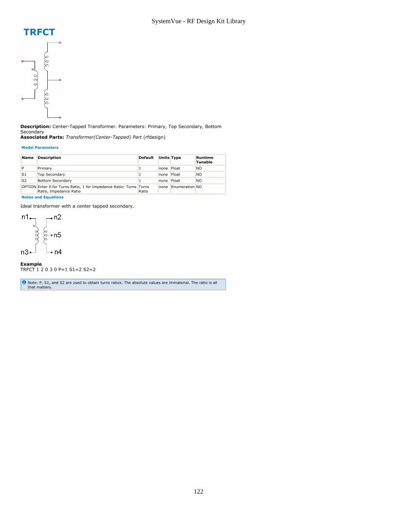
SystemVue - RF Design Kit Library
122
TRFCT
Description: Center-Tapped Transformer. Parameters: Primary, Top Secondary, BottomSecondaryAssociated Parts: Transformer(Center-Tapped) Part (rfdesign)
Model Parameters
Name Description Default Units Type RuntimeTunable
P Primary 1 none Float NO
S1 Top Secondary 1 none Float NO
S2 Bottom Secondary 1 none Float NO
OPTION Enter 0 for Turns Ratio, 1 for Impedance Ratio: TurnsRatio, Impedance Ratio
TurnsRatio
none Enumeration NO
Notes and Equations
Ideal transformer with a center tapped secondary.
ExampleTRFCT 1 2 0 3 0 P=1 S1=2 S2=2
Note: P, S1, and S2 are used to obtain turns ratios. The absolute values are immaterial. The ratio is allthat matters.

SystemVue - RF Design Kit Library
123
Transformer Part Transformer. Parameters: Primary, Secondary, Conditioning Factor
Categories: Lumped (rfdesign)
The models associated with this part are listed below. To view detailed information on amodel (description, parameters, equations, notes, etc.), please click the appropriate link.
Model
TRF (rfdesign)

SystemVue - RF Design Kit Library
124
TRF
Description: Transformer. Parameters: Primary, Secondary, Conditioning FactorAssociated Parts: Transformer Part (rfdesign)
Model Parameters
Name Description Default Units Type RuntimeTunable
P Primary 1 Integer NO
S Secondary 1 Integer NO
OPTION Enter 0 for Turns Ratio, 1 for Impedance Ratio: TurnsRatio, Impedance Ratio
TurnsRatio
Enumeration NO
Notes and Equations
Netlist SyntaxTRF n1 n2 n3 n4 Option={TR|IM} Primary= [Secondary=] [Condition=] [Name=]
Additional Information
Primary # turns on primary (TR) or primary impedance (IM).Secondary # turns on secondary (TR) or sec. impedance (IM). This parameter isoptional, and defaults to 1 if not specified.TR: Turns Ratio Choose this option to specify a turns ratio.IM: Impedance Ratio Choose this option to specify an impedance ratio.
ExampleTRF 1 2 0 0 Option=IM P=200 S=50
The turns and impedance are relative. For example, 200 and 50 will have the same resultas 4 and 1. If an inverting transformer is desired, primary is negative. An idealtransformer can ill-condition the matrix Genesys must solve. This causes the red error barto illuminate. To eliminate this problem, certain networks using TRF may require aconditioning factor, typically 0.001 to.1.
Touchstone TranslationXFER n1 n2 n3 n4 N=

SystemVue - RF Design Kit Library
125
Mixer Part Basic Mixer
Categories: Mixers (rfdesign), System (rfdesign)
The models associated with this part are listed below. To view detailed information on amodel (description, parameters, equations, notes, etc.), please click the appropriate link.
Model
MIXER_BASIC (rfdesign)
MIXER_TBL (rfdesign)
MIXER_DBAL (rfdesign)
MIXER_BASIC
Description: Basic MixerAssociated Parts: Mixer Part (rfdesign)
Model Parameters
Name Description Default Units Type RuntimeTunable
ConvGain Conversion Gain -8 dB Integer NO
SUM Desired Output: 0-Difference, 1-Sum 0 Integer NO
LO LO Drive Level 7 dBm Integer NO
NF Noise Figure none dB Integer NO
IP1dB Input P1dB 1 dBm Integer NO
IPSAT Input Saturation Power 2 dBm Integer NO
IIP3 Input IP3 11 dBm Integer NO
IIP2 Input IP2 21 dBm Integer NO
LOHarms LO Harmonics in dB below LOfundamental
[30;10] dB Integer NO
Show_More_Parameters Show More Parameters 0 Integer NO
ISIDE Image Side to Reject: 0-Below, 1-Above LO
0 Integer NO
IR Image Rejection 0 dB Integer NO
RTOI RF to IF Isolation 100 dB Integer NO
LTOR LO to RF Isolation 30 dB Integer NO
LTOI LO to IF Isolation 30 dB Integer NO
InRevIso Out to In Reverse Isolation 300 dB Integer NO
LORevIso Out to LO Reverse Isolation 300 dB Integer NO
ZR RF Port Input Impedance 50 ohm Integer NO
ZI IF Port Input Impedance 50 ohm Integer NO
ZL LO Port Input Impedance 50 ohm Integer NO
Show_Advanced_Parameters Show Advanced Parameters 0 Integer NO
OperationMode Mode of Operation 0 Integer NO
ImageSelfNoise Image Self Noise Scale Factor 1 Integer NO
The basic mixer can be used as both an active or passive mixer. Both sum and differenceproducts will always be created. The maximum order of products created at the output isdetermined by the Maximum Order property, which is set on the Calculate Tab in theSystem Analysis. Harmonics of the LO used in the mixing process is determined by gettingthe Fourier coefficients of a near square wave (52% duty cycle) and scaling them relativeto the LO power. The LO along with all its harmonics are mixed with every input signal toproduce both sum and difference frequencies. The operating point of the mixer isdetermined by the total RF and IF power driving the mixer. The mixer does know anddoesn't care whether it is being driven from the RF or IF ports. As a matter of factspectrums will propagate from the RF port to the IF port and vice versa. When multiplespectrums arrive at the RF or IF ports these spectrums generate intermods and harmonicswhich will be mixed with each harmonic of the LO.
Thermal noise arriving at the RF or IF is not mixed and does not create intermods andharmonics. However, this thermal noise will be folded at the LO frequency and extendedto the maximum simulation frequency (Ignore Frequency Above). This processautomatically accounts for noise at the image frequency.
Phase noise is also processed by the mixer. Mixed output spectrum is a combination of theinput and LO spectrum phase noise.
This mixer can also be used to as an ideal image reject mixer. This is very handy whendebugging image related RF architecture issues.
This mixer also has the ability to deal with reverse isolation. Mixed spectrum created bythe mixer can be placed back at the mixer input as well as the LO. The amount of isolationcan be controlled by the user.
WARNING: The LO power level must be within the tolerance range of the target 'LO Drive Level' or nomixed spectrum will be created!

SystemVue - RF Design Kit Library
126
NOTE: Compression effects of the LO drive are not accounted for in this model. Amplitudes of LOharmonics and intermods are strictly based on Fourier coefficients as described above.
Additional Parameter Information
DesiredOutput(SUM)
The parameter is used by Spectrasys to determine the correct channel frequency to use at themixer output. When set to 0 the channel frequency at the output will be the difference betweenthe channel frequency at the input minus the peak LO frequency. When set to 1 the channelfrequency at the input will be the sum of the input channel frequency and the peak LOfrequency. This parameter has no bearing on what type of mixed spectrums are created at themixer output. Both sum and difference spectrum will always be created.
Image Sideto Reject(ISIDE)
The mixer image frequency will be either above or below the LO center frequency for alldifference products. When this parameter is set to 0 all frequencies of the input spectrum thatare below the LO frequency will be attenuated by the image rejection amount. When set to 1 allfrequencies of the input spectrum above the LO frequency, up to the maximum frequency of thespectrum will be attenuated by the image rejection amount.
For all sumproducts
the image frequency is that frequency where a difference will fall at the mixer sum frequency.For example, if the mixer input frequency was 1000 MHz with an LO frequency of 900 MHz a100 MHz difference and 1900 MHz sum products would be created. If the desired output is the1900 MHz sum then a 2800 MHz input frequency would be the image to the 1000 MHz inputsignal since 2800 - 900 MHz = 1900 MHz. For sum products the image side is irrelevant sincethe image will always be higher than the LO frequency. This image will always be greater thanthe desired input frequency. Consequently, image rejection for a sum product is defined as anyinput frequency which is greater than the frequency of the peak input signal.
ImageRejection(IR)
The amount of image rejection. When set to a nonzero value ALL spectrums, including noise,will be attenuated by this amount. The spectrum frequencies that will be attenuated aredescribed in the 'Image Side to Reject' explanation.
InputSaturationPower(IPSAT)
Input level at which the mixer will saturate.
Input 2ndOrderIntercept(IIP2)
This intercept point is referenced to intermods and not harmonics. See Second Order InterceptDifferences for Mixers and Amplifiers for additional information.
Note: If the input saturation is greater than about 9 dB above the input 1 dB compression point thesaturation power will be set to 3 dB above the 1 dB compression point.
Out to InReverse Isolation(InRevIso)
This parameter controls the power level of the intermods and harmonics that will appearback on the input port and propagate backwards through the system. This parameterapplies to both the RF port and IF port. IF output spectrum created by the RF and LO portsignals will appear at the RF port and RF output spectrum created by the IF and LO portsignals will appear at the IF port.
Out to LOReverse Isolation(LORevIso)
This parameter controls the power level of the intermods and harmonics that will appear onthe LO port and propagate backwards through the system. This parameter applies to boththe RF port and IF port. IF output spectrum created by the RF and LO port signals willappear at the LO port as well as the RF output spectrum created by the IF and LO portsignals.
Additional Operation Information
LO Drive Level
The LO drive level does not affect the power level of any of the spectrums created by themixer other than the port to port isolation spectrum. However, Spectrasys will look at thispower level during the simulation and warn the user if the power level is outside thetolerance range specified in the 'System Analysis'. No spectrum at the output will becreated unless the LO power level is within this tolerance range.
Mixed Spectrum Creation
Several spectrums may be present on the LO port of a mixer. Spectrasys has the ability touse only the peak LO signal or all LO signals that fall within a given power level range ofthe peak LO signal. See the 'Options Tab' of the 'System Simulation Dialog Box' for moreinformation of this setting.
Isolation Spectrum
All signals arriving at any mixer port will be propagated to the other mixer ports throughtheir respective isolation's.
Reverse Isolation
The mixer will create reverse isolation products on the mixer RF and IF ports based on thereverse isolation parameters.
Mixer Thermal Noise Model
Thermal noise arriving at the RF or IF is not mixed and does not create intermods andharmonics. Noise arriving at the input is separated into 2 frequency bands. One below theLO frequency and the other above it. Depending on the mixer Input and LO frequenciesone band will be in the main desired band of frequencies and the other will be in theimage band. The location of these bands is determined by the 'LO Side to Reject'parameter. Frequencies falling into the Image band will be rejected by the 'ImageRejection' parameter. By default the image rejection is 0 dB. The mixer also generatesself noise at both the main or desired frequency as well as the image frequency. Theamount of self noise at the image frequency can controlled with the ImageSelfNoiseparameter. This self noise is added to the input noise and then amplified by theconversion gain of the mixer at the main frequency and image frequency. All the noise issummed together at the mixer output.

SystemVue - RF Design Kit Library
127
NoteThe main and image band conversion gains for behavioral mixer models are identical.
CautionImage rejection does not affect the image self noise generated by the mixer. Image rejection only appliesto noise signals appearing at the mixer input. Traditional cascaded noise measurements completelyignore both the mixer input noise at the image frequency and the mixer self generated noise at the imagefrequency.
Phase Noise
Phase noise is also processed by the mixer. Mixed output spectrum inherit the phase noiseof the LO. When input spectrum have phase noise and there is no LO phase noise specifiedthen the mixed spectrum will retain the phase noise of the input spectrum.
Phase
Output Phase = LO Phase + Input Phase (Sum)Output Phase = LO Phase - Input Phase (Difference for High LO Side Injection )Output Phase = Input Phase - LO Phase (Difference for Low LO Side Injection )
Output Intermod and Harmonic Phase
The output phase of an intermod is based on the phase of the input signals and thecoefficients of the intermod equation. However, the polynomial coefficients that representthe Vin versus Vout curve have negative coefficients for all odd orders 3rd and higher.This means that odd orders of 3rd and higher will have a phase shift of 180 degrees.These negative odd coefficients keep the transfer function from increasing monotonically. Output Phase = +/- K * Input1Phase +/- M * Input 2 Phase +/- N * Input 3 Phase ... Where K, M, N, etc are the coefficients of the intermod equation. For example, the phase of the 2nd harmonic will be double the input phase, triple theinput phase plus 180 degrees for a 3rd harmonic etc.
Image Frequency
The image frequency is an alternate frequency at the input of the mixer that will producesthe same IF output frequency as the desired input frequency. For example, if the desiredmixer input signal is 800 MHz with an LO frequency of 900 MHz then the difference IFoutput frequency is 100 MHz. However, a input frequency of 1000 MHz when mixed withthe same 900 MHz LO will also produce a 100 MHz IF frequency. The 1000 MHz is theimage of the desired 800 MHz input frequency.
Image Frequencies are located at the following frequencies:
Sum: Fimage = 2 * Flo +Frf
Difference: Fimage = 2 * Flo - Frf
Orders Generated by Multiple Input Spectrums
When multiple spectrums arrive at the RF or IF ports they will generate intermods andharmonics based on the nonlinear transfer function defined by the nonlinear parameters(IP1dB, IPSAT, IIP3, IIP2). A maximum of 3 orders will be created since these nonlinearparameters only support a 3rd order transfer function. However, this should not beconfused with the maximum order of the mixer output products. The input products orderis limited to 3 but higher order LO products can be used until the maximum simulationorder is reached.
SVNI
(Stage Equivalent Input Noise Measurement) - Voltage Based)
When the voltage based measurement SVNI is used on this mixer the real value of the RFport input impedance is used to determine the source resistance.

SystemVue - RF Design Kit Library
128
Input Self Mixing
Mixer input signals leak to the LO and will mix with themselves in non-ideal mixers. This iscalled RF ( or input self mixing since the input port can be the IF port ) self mixing. TheDC value output is = 2 x Signal Input Power - Mixer IIP2 (dBm). The bandwidth of thespectrum at DC will be the same bandwidth as the mixer input spectrum. Since a 2ndharmonic has double the bandwidth of the fundamental and the self mixing product existsat DC, only the positive half of the intermod will be seen which is equivalent to the inputspectrum bandwidth.
DC Block
DC is blocked.
WARNING: Only the linear portion of this model is used in simulators other than Spectrasys. The linearmodel is the port impedance coupled with the isolation parameters.
NOTE: RF to IF isolation is used not the conversion gain. Conversion gain is not used since this is anonlinear process.
Double Balanced Mixer [MIXER_DBAL]
This model is based on the work of Bert Henderson at Watkins Johnson. The name of theapplication note discussing this is, "Predicting Intermodulation Suppression in Double-Balanced Mixers";. This mixer can be used for both an active and passive mixer. However,the model itself was derived from a passive double balanced mixer. Both sum anddifference products will always be created. The maximum order of products created at theoutput is determined by the Maximum Order property in the System Analysis. Theoperating point of the mixer is determined by the total RF and IF power driving the mixer.The mixer does know and doesn't care whether it is being driven from the RF or IF ports.As a matter of fact spectrums will propagate from the RF port to the IF port and viceversa. This double balanced mixer model is applied to the mixer in both directions. Thismeans that RF input signals will be combined with the LO to produce intermods at the IFport. Likewise, IF input signals will be combined with the LO to produce intermods at theRF port. This module doesn't support intermod products created by multiple input signals.
Since this model doesn't deal with harmonics of the LO an approximation is used dodetermine there amplitudes. The LO fundamental isolation is based on the LO balunisolation. The harmonics of the LO are based on the Fourier coefficients of a near squarewave (52% duty cycle) and scaling them relative to the LO power.
Thermal noise arriving at the RF or IF is not mixed and does not create intermods andharmonics. However, this thermal noise will be folded at the LO frequency and extendedto the maximum simulation frequency (Ignore Frequency Above). This processautomatically accounts for noise at the image frequency.
Phase noise is also processed by the mixer. Mixed output spectrum is a combination of theinput and LO spectrum phase noise.
This mixer can also be used to as an ideal image reject mixer. This is very handy whendebugging image related RF architecture issues.
This mixer also has the ability to deal with reverse isolation. Mixed spectrum created bythe mixer can be placed back at the mixer input as well as the LO. The amount of isolationcan be controlled by the user.
NoteThe LO power level must be within the tolerance range of the target 'LO Drive Level' or no mixed spectrumwill be created!
Description: Basic MixerAssociated Parts: Mixer Part (rfdesign)
Model Parameters
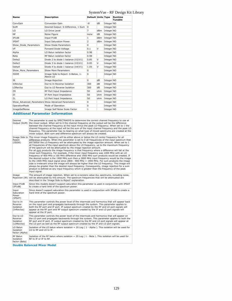
SystemVue - RF Design Kit Library
129
Name Description Default Units Type RuntimeTunable
ConvGain Conversion Gain -8 dB Integer NO
SUM Desired Output: 0-Difference, 1-Sum 0 Integer NO
LO LO Drive Level 7 dBm Integer NO
NF Noise Figure none dB Integer NO
IP1dB Input P1dB 1 dBm Integer NO
IPSAT Input Saturation Power 2 dBm Integer NO
Show_Diode_Parameters Show Diode Parameters 0 Integer NO
VF Forward Diode Voltage 0.1 V Integer NO
Alpha LO Balun isolation factor 0.98 Integer NO
Beta RF Balun isolation factor 0.98 Integer NO
Delta2 Diode 2 to diode 1 balance (V2/V1) 0.85 V Integer NO
Delta3 Diode 3 to diode 1 balance (V3/V1) 0.95 V Integer NO
Delta4 Diode 4 to diode 1 balance (V4/V1) 1.05 V Integer NO
Show_More_Parameters Show More Parameters 0 Integer NO
ISIDE Image Side to Reject: 0-Below, 1-Above LO
0 Integer NO
IR Image Rejection 0 dB Integer NO
InRevIso Out to In Reverse Isolation 300 dB Integer NO
LORevIso Out to LO Reverse Isolation 300 dB Integer NO
ZR RF Port Input Impedance 50 ohm Integer NO
ZI IF Port Input Impedance 50 ohm Integer NO
ZL LO Port Input Impedance 50 ohm Integer NO
Show_Advanced_Parameters Show Advanced Parameters 0 Integer NO
OperationMode Mode of Operation 0 Integer NO
ImageSelfNoise Image Self Noise Scale Factor 1 Integer NO
Additional Parameter Information
DesiredOutput (SUM)
The parameter is used by SPECTRASYS to determine the correct channel frequency to use atthe mixer output. When set to 0 the channel frequency at the output will be the differencebetween the channel frequency at the input minus the peak LO frequency. When set to 1 thechannel frequency at the input will be the sum of the input channel frequency and the peak LOfrequency. This parameter has no bearing on what type of mixed spectrums are created at themixer output. Both sum and difference spectrum will always be created.
Image Side toReject(ISIDE)
The mixer image frequency will be either above or below the LO center frequency for alldifference products. When this parameter is set to 0 all frequencies of the input spectrum thatare below the LO frequency will be attenuated by the image rejection amount. When set to 1all frequencies of the input spectrum above the LO frequency, up to the maximum frequencyof the spectrum will be attenuated by the image rejection amount.For all sum products the image frequency is that frequency where a difference will fall at themixer sum frequency. For example, if the mixer input frequency was 1000 MHz with an LOfrequency of 900 MHz a 100 MHz difference and 1900 MHz sum products would be created. Ifthe desired output is the 1900 MHz sum then a 2800 MHz input frequency would be the imageto the 1000 MHz input signal since 2800 - 900 MHz = 1900 MHz. For sum products the imageside is irrelevant since the image will always be higher than the LO frequency. This image willalways be greater than the desired input frequency. Consequently, image rejection for a sumproduct is defined as any input frequency which is greater than the frequency of the peakinput signal.
ImageRejection (IR)
The amount of image rejection. When set to a nonzero value ALL spectrums, including noise,will be attenuated by this amount. The spectrum frequencies that will be attenuated aredescribed in the 'Image Side to Reject' explanation.
Input P1dB(IP1dB)
Since this models doesn't support saturation this parameter is used in conjunction with IPSATto create a hard limit of the spectrum power.
InputSaturationPower(IPSAT)
Since doesn't support saturation this parameter is used in conjunction with IP1dB to create ahard limit of the spectrum power.
Out to InReverseIsolation(InRevIso)
This parameter controls the power level of the intermods and harmonics that will appear backon the input port and propagate backwards through the system. This parameter applies toboth the RF port and IF port. IF output spectrum created by the RF and LO port signals willappear at the RF port and RF output spectrum created by the IF and LO port signals willappear at the IF port.
Out to LOReverseIsolation(LORevIso)
This parameter controls the power level of the intermods and harmonics that will appear onthe LO port and propagate backwards through the system. This parameter applies to both theRF port and IF port. IF output spectrum created by the RF and LO port signals will appear atthe LO port as well as the RF output spectrum created by the IF and LO port signals.
LO BalunIsolationfactor (Alpha)
Isolation of the LO balun where isolation = 20 Log ( 1 - Alpha ). This isolation will be used forLO to RF and LO to IF.
RF BalunIsolationfactor (Beta)
Isolation of the RF balun where isolation = 20 Log ( 1 - Beta ). This isolation will be used forRF to IF or IF to RF.
Double Balanced Mixer Model

SystemVue - RF Design Kit Library
130
For additional information on balun and diode voltage parameters please refer to theapplication note from Watkins Johnson.
Additional Operation Information:
LO Drive Level
SPECTRASYS will look at this power level during the simulation and warn the user if thepower level is outside the tolerance range specified in the 'System Analysis'. No spectrumat the output will be created unless the LO power level is within this tolerance range.
Mixed Spectrum Creation
Several spectrums may be present on the LO port of a mixer. SPECTRASYS has the abilityto use only the peak LO signal or all LO signals that fall within a given power level rangeof the peak LO signal. See the 'Options Tab' of the 'System Simulation Dialog Box' formore information of this setting.
Isolation Spectrum
All signals arriving at any mixer port will be propagated to the other mixer ports throughtheir respective isolations.
Reverse Isolation
The mixer will create reverse isolation products on the mixer RF and IF ports based on thereverse isolation parameters.
Thermal Noise
Thermal noise arriving at the RF or IF is not mixed and does not create intermods andharmonics. However, this thermal noise will be folded at the LO frequency and extendedto the maximum simulation frequency (Ignore Frequency Above). This processautomatically accounts for noise at the image frequency.
Phase Noise
Phase noise is also processed by the mixer. Mixed output spectrum inherit the phase noiseof the LO. When input spectrum have phase noise and there is no LO phase noise specifiedthen the mixed spectrum will retain the phase noise of the input spectrum.
Multiple Input Spectrum
This model will does not have the ability to generate intermods and harmonics frommultiple input spectrums before being mixed with harmonics of the LO. Consequently,each input spectrum will be processed one at a time.
Phase
Output Phase = LO Phase + Input Phase (Sum)Output Phase = LO Phase - Input Phase (Difference for High LO Side Injection )Output Phase = Input Phase - LO Phase (Difference for Low LO Side Injection )
Output Intermod and Harmonic Phase
The output phase of an intermod is based on the phase of the input signals and thecoefficients of the intermod equation. However, the polynomial coefficients that representthe Vin versus Vout curve have negative coefficients for all odd orders 3rd and higher.This means that odd orders of 3rd and higher will have a phase shift of 180 degrees.These negative odd coefficients keep the transfer function from increasing monotonically.
Output Phase = +/- K * Input1Phase +/- M * Input 2 Phase +/- N * Input 3 Phase ...
Where K, M, N, etc are the coefficients of the intermod equation.
For example, the phase of the 2nd harmonic will be double the input phase, triple the
SystemVue - RF Design Kit Library
131
input phase plus 180 degrees for a 3rd harmonic etc.
Image Frequency
The image frequency is a frequency at the input of the mixer that will produce the samedifference IF output frequency as the desired input frequency. For example, if the desiredmixer input signal is 800 MHz with an LO frequency of 900 MHz then the difference IFoutput frequency is 100 MHz. However, a input frequency of 1000 MHz when mixed withthe same 900 MHz LO will also produce a 100 MHz IF frequency. The 1000 MHz is theimage of the desired 800 MHz input frequency.
SVNI
(Stage Equivalent Input Noise Measurement- Voltage Based)When the voltage based measurement SVNI is used on this mixer the real value of the RFport input impedance is used to determine the source resistance.
DC Block
DC is blocked
CautionOnly the linear portion of this model is used in simulators other than Spectrasys. The linear model is theport impedance coupled with the isolation parameters.
NoteRF to IF isolation is used not the conversion gain. Conversion gain is not used since this is a nonlinearprocess.
NoteThe maximum mixer / intermod order is 25.
MIXER_TBL
Description: Basic MixerAssociated Parts: Mixer Part (rfdesign)
Model Parameters

SystemVue - RF Design Kit Library
132
Name Description Default Units Type RuntimeTunable
ConvGain ConversionGain
-8 dB Integer NO
SUM DesiredOutput: 0-Difference,1-Sum
0 Integer NO
LO LO DriveLevel
7 dBm Integer NO
NF Noise Figure none dB Integer NO
IP1dB Input P1dB 1 dBm Integer NO
IPSAT InputSaturationPower
2 dBm Integer NO
Show_Table_Parameters Show TableParameters
0 Integer NO
RFTableData RF -> IFTable Data
[6;300;0;29;23;42;25;20;0;29;12;34;25;52;40;58;40;58;41;46;49;50;49;53;49;73;73;65;62;66;59;77;76;84;63;64;60] Integer NO
RFTableInPwr RF Power forRF -> IFTable
-20 dBm Integer NO
RFTableLOPwr LO Power forRF -> IFTable
10 dBm Integer NO
RFTableDefSup DefaultSuppressionfor RF -> IFTable
300 dB Integer NO
RFTableLOOnly Use RFTable for LOHarmonicsOnly
0 Integer NO
RFTableUnits Units of RFTable
0 Integer NO
IFTableData IF -> RFTable Data
[1;300;20;30;40] Integer NO
IFTableInPwr IF Power forIF -> RFTable
-20 dBm Integer NO
IFTableLOPwr LO Power forIF -> RFTable
10 dBm Integer NO
IFTableDefSup DefaultSuppressionfor IF -> RFTable
300 dB Integer NO
IFTableLOOnly Use IF Tablefor LOHarmonicOnly
1 Integer NO
IFTableUnits Units of IFTable
0 Integer NO
Show_More_Parameters Show MoreParameters
0 Integer NO
ISIDE Image Sideto Reject: 0-Below, 1-Above LO
0 Integer NO
IR ImageRejection
0 dB Integer NO
InRevIso Out to InReverseIsolation
300 dB Integer NO
LORevIso Out to LOReverseIsolation
300 dB Integer NO
ZR RF PortInputImpedance
50 ohm Integer NO
ZI IF Port InputImpedance
50 ohm Integer NO
ZL LO PortInputImpedance
50 ohm Integer NO
Show_Advanced_Parameters ShowAdvancedParameters
0 Integer NO
OperationMode Mode ofOperation
0 Integer NO
ImageSelfNoise Image SelfNoise ScaleFactor
1 Integer NO
The mixer model uses a user defined intermod table to produce mixer output intermodsbetween the input spectrum and the LO spectrum. A independent table is used for inputspectrums arriving at the RF port and another one for spectrums arriving at the IF port.
This mixer can be used for both an active and passive mixer. Both sum and differenceproducts will always be created. The maximum order of products created at the output is
SystemVue - RF Design Kit Library
133
determined by the 'Maximum Order' property on the Calculate Tab in the System Analysis.The operating point of the mixer is determined by the sum of the total RF and IF powerdriving the mixer. The mixer doesn't know and doesn't care whether it is being drivenfrom the RF or IF ports. As a matter of fact spectrums will propagate from the RF port tothe IF port and vice versa. There are two intermod tables in this mixer that specify all theproducts created at the IF port from the RF and LO ports and those created at the RF portfrom the LO and IF ports. This means that there is one table where RF input signals will becombined with the LO to produce intermods at the IF port. Likewise, the other tablecontains IF input signals that will be combined with the LO to produce intermods at the RFport. Generally, the mixer table representing the reverse direction of the intended flowcan be used to only specify harmonics of the LO if desired.
This model doesn't support intermod products created by multiple input signals.
Thermal noise arriving at the RF or IF does not create intermods and harmonics. However,this thermal noise will be folded at the LO frequency and extended to the maximumsimulation frequency (Ignore Frequency Above). This process automatically accounts fornoise at the image frequency.
Phase noise is also processed by the mixer. Mixed output spectrum is a combination of theinput and LO spectrum phase noise.
This mixer can also be used to as an ideal image reject mixer. This is very handy whendebugging image related RF architecture issues.
This mixer also has the ability to deal with reverse isolation. Mixed spectrum created bythe mixer can be placed back at the mixer input as well as the LO. The amount of isolationcan be controlled by the user.
WarningThe LO power level must be within the tolerance range (sim) of the target 'LO Drive Level' or no mixedspectrum will be created!
NoteThe conversion gain is not affected by LO drive level in this model.
Additional Parameter Information
Common Parameters
DesiredOutput ( SUM)
The parameter is used by Spectrasys to determine the correct channel frequency to use at themixer output. When set to 0 the channel frequency at the output will be the difference betweenthe channel frequency at the input minus the peak LO frequency. When set to 1 the channelfrequency at the input will be the sum of the input channel frequency and the peak LOfrequency. This parameter has no bearing on what type of mixed spectrums are created at themixer output. Both sum and difference spectrum will always be created.
Input P1dB (IP1dB )
Since intermod tables only contain intermod information at the input and LO characterizationlevels this parameter is used in conjunction with IPSAT to create a hard limit of the spectrumpower.
InputSaturationPower (IPSAT )
Since intermod tables only contain intermod information at the input and LO characterizationlevels this parameter is used in conjunction with IP1dB to create a hard limit of the spectrumpower.
Table Parameters
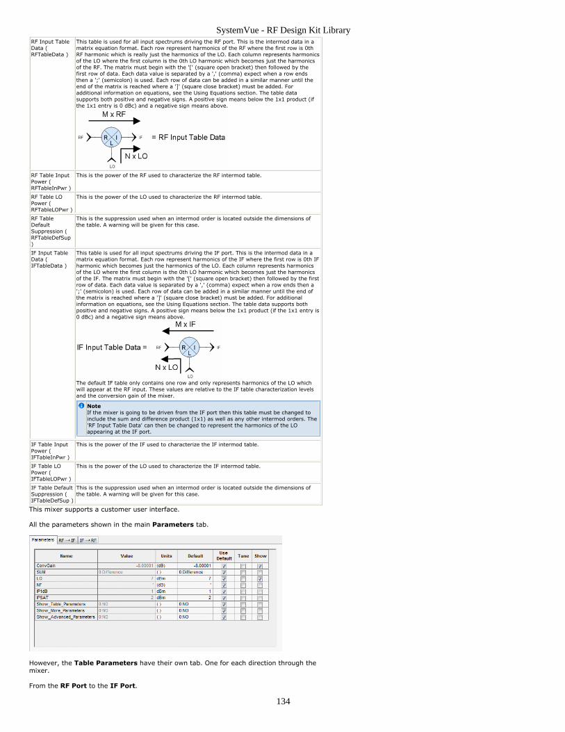
SystemVue - RF Design Kit Library
134
RF Input TableData (RFTableData )
This table is used for all input spectrums driving the RF port. This is the intermod data in amatrix equation format. Each row represent harmonics of the RF where the first row is 0thRF harmonic which is really just the harmonics of the LO. Each column represents harmonicsof the LO where the first column is the 0th LO harmonic which becomes just the harmonicsof the RF. The matrix must begin with the '[' (square open bracket) then followed by thefirst row of data. Each data value is separated by a ',' (comma) expect when a row endsthen a ';' (semicolon) is used. Each row of data can be added in a similar manner until theend of the matrix is reached where a ']' (square close bracket) must be added. Foradditional information on equations, see the Using Equations section. The table datasupports both positive and negative signs. A positive sign means below the 1x1 product (ifthe 1x1 entry is 0 dBc) and a negative sign means above.
RF Table InputPower (RFTableInPwr )
This is the power of the RF used to characterize the RF intermod table.
RF Table LOPower (RFTableLOPwr )
This is the power of the LO used to characterize the RF intermod table.
RF TableDefaultSuppression (RFTableDefSup)
This is the suppression used when an intermod order is located outside the dimensions ofthe table. A warning will be given for this case.
IF Input TableData (IFTableData )
This table is used for all input spectrums driving the IF port. This is the intermod data in amatrix equation format. Each row represent harmonics of the IF where the first row is 0th IFharmonic which becomes just the harmonics of the LO. Each column represents harmonicsof the LO where the first column is the 0th LO harmonic which becomes just the harmonicsof the IF. The matrix must begin with the '[' (square open bracket) then followed by the firstrow of data. Each data value is separated by a ',' (comma) expect when a row ends then a';' (semicolon) is used. Each row of data can be added in a similar manner until the end ofthe matrix is reached where a ']' (square close bracket) must be added. For additionalinformation on equations, see the Using Equations section. The table data supports bothpositive and negative signs. A positive sign means below the 1x1 product (if the 1x1 entry is0 dBc) and a negative sign means above.
The default IF table only contains one row and only represents harmonics of the LO whichwill appear at the RF input. These values are relative to the IF table characterization levelsand the conversion gain of the mixer.
NoteIf the mixer is going to be driven from the IF port then this table must be changed toinclude the sum and difference product (1x1) as well as any other intermod orders. The'RF Input Table Data' can then be changed to represent the harmonics of the LOappearing at the IF port.
IF Table InputPower (IFTableInPwr )
This is the power of the IF used to characterize the IF intermod table.
IF Table LOPower (IFTableLOPwr )
This is the power of the LO used to characterize the IF intermod table.
IF Table DefaultSuppression (IFTableDefSup )
This is the suppression used when an intermod order is located outside the dimensions ofthe table. A warning will be given for this case.
This mixer supports a customer user interface.
All the parameters shown in the main Parameters tab.
However, the Table Parameters have their own tab. One for each direction through themixer.
From the RF Port to the IF Port.

SystemVue - RF Design Kit Library
135
And the IF Port to the RF Port.
NoteThe table going in the reverse direction generally just represents the spurious products that will beleaked backwards through the system to the input.
.
The power levels shown on the table tabs are the power levels at which the table wascharacterized at.
TipAny table entries left empty will be replaced with the Default Entry.
Table values can be displayed either in dBc (dB below the 1x1 product) or dBm.
CautionInternally the table data is always stored in dBc. The unit dBm is for display purposes only. When thedialog is opened or closed a translation takes place between dBc and dBm as appropriate. The conversionbetween dBc and dBm only occurs if a number is detected in the table cell. If an equation variable is usedthe conversion does not take place and the equation values are assumed to be in dBc.
When the Use Table for LO Harmonics is checked only the first row of the table will beused which is just the harmonics of the LO.
Image Parameters
ImageSide toReject(ISIDE)
The mixer image frequency will be either above or below the LO center frequency for all differenceproducts. When this parameter is set to 0 all frequencies of the input spectrum that are below theLO frequency will be attenuated by the image rejection amount. When set to 1 all frequencies ofthe input spectrum above the LO frequency, up to the maximum frequency of the spectrum will beattenuated by the image rejection amount. For all sum products the image frequency is thatfrequency where a difference will fall at the mixer sum frequency. For example, if the mixer inputfrequency was 1000 MHz with an LO frequency of 900 MHz a 100 MHz difference and 1900 MHzsum products would be created. If the desired output is the 1900 MHz sum then a 2800 MHz inputfrequency would be the image to the 1000 MHz input signal since 2800 - 900 MHz = 1900 MHz.For sum products the image side is irrelevant since the image will always be higher than the LOfrequency. This image will always be greater than the desired input frequency. Consequently,image rejection for a sum product is defined as any input frequency which is greater than thefrequency of the peak input signal.
ImageRejection(IR)
The amount of image rejection. When set to a nonzero value ALL spectrums, including noise, willbe attenuated by this amount. The spectrum frequencies that will be attenuated are described inthe 'Image Side to Reject' explanation.
Isolation Parameters
Out to InReverseIsolation (InRevIso )
This parameter controls the power level of the intermods and harmonics that will appearback on the input port and propagate backwards through the system. This parameter appliesto both the RF port and IF port. IF output spectrum created by the RF and LO port signalswill appear at the RF port and RF output spectrum created by the IF and LO port signals willappear at the IF port.
Out to LOReverseIsolation (LORevIso )
This parameter controls the power level of the intermods and harmonics that will appear onthe LO port and propagate backwards through the system. This parameter applies to boththe RF port and IF port. IF output spectrum created by the RF and LO port signals willappear at the LO port as well as the RF output spectrum created by the IF and LO portsignals.
Advanced Parameters
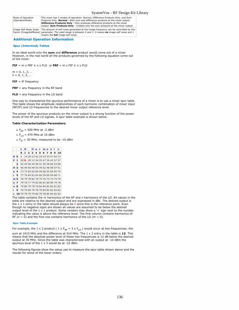
SystemVue - RF Design Kit Library
136
Mode of Operation(OperationMode)
The mixer has 3 modes of operation: Normal, Difference Products Only, and SumProducts Only. Normal - Both sum and difference products at the mixer output.Difference Products Only - Only produces difference products at the mixeroutput. Sum Products Only - Creates only the sum products at the mixer output.
Image Self Noise ScaleFactor (ImageSelfNoise)
The amount of self noise generated at the image frequency can be controlled by thisparameter. The valid range is between 0 and 1. 0 means no image self noise and 1means the full image self noise.
Additional Operation Information
Spur (Intermod) Tables
In an ideal world only the sum and difference product would come out of a mixer.However, in the real world all the products governed by the following equation come outof the mixer.
FIF = m x FRF ± n x FLO or FRF = m x FIF ± n x FLO
m = 0, 1, 2, …n = 0, 1, 2, …
FIF = IF frequency
FRF = any frequency in the RF band
FLO = any frequency in the LO band
One way to characterize the spurious performance of a mixer is to use a mixer spur table.This table shows the amplitude relationships of each harmonic combination of mixer input(RF/IF) and LO frequencies to the desired mixer output reference level.
The power of the spurious products on the mixer output is a strong function of the powerlevels of the RF and LO signals. A spur table example is shown below.
Table Characterization Parameters:
FRF = 500 MHz at -2 dBm
FLO = 470 MHz at 10 dBm
FIF = 30 MHz, measured to be -10 dBm
L O H a r m o n i c
0 1 2 3 4 5 6 7 8 9 10
R 0 X 14 29 23 42 25 43 53 57 65 72
F 1 20 0 29 12 34 25 47 35 42 57 57
2 52 40 58 40 58 41 50 48 66 53 68
H 3 46 49 50 49 53 49 52 48 58 57 51
a 4 73 73 65 62 66 59 66 55 65 65 70
r 5 77 76 84 63 64 60 59 60 59 68 71
m 6 78 79 78 82 79 79 76 75 75 74 79
o 7 79 78 77 79 82 80 81 80 80 79 78
n 8 79 80 79 78 78 84 84 82 82 81 82
i 9 79 79 80 79 78 79 84 84 82 83 82
c 10 79 79 79 79 80 79 78 84 84 82 83
The table contains the m harmonics of the RF and n harmonics of the LO. All values in thetable are relative to the desired output and are expressed in dBc. The desired output isthe 1 x 1 entry in the table should always be 0 since this is the reference point. Eventhough no negative signs are shown all values are assumed to be below the desiredoutput level of the 1 x 1 product. Some vendors may show a '+' sign next to the numberindicating the value is above the reference level. The first column contains harmonics ofRF (n = 0) and the first row contains harmonics of the LO (m = 0).
Spur Table Example
For example, the 1 x 3 product ( 1 x FRF + 3 x FLO ) would occur at two frequencies: the
sum at 1910 MHz and the difference at 910 MHz. The 1 x 3 entry in the table is 12. Thismeans that the absolute power level of these two frequencies is 12 dB below the desiredoutput at 30 MHz. Since the table was characterized with an output at -10 dBm thespurious level of the 1 x 3 would be at -22 dBm.
The following figures show the setup use to measure the spur table shown above and theresults for some of the lower orders.

SystemVue - RF Design Kit Library
137
Input Power Rolloff
NoteTheoretically, the 'm x FRF' or 'm x FIF' products will decrease (m-1) dB for each dB the input power (RFor IF) is decreased below the RF (IF) characterization level of the spur table.
The following table shows how the relative power changes at the mixer output when theinput power is dropped by 1 dB.
L O H a r m o n i c
0 1 2 3 4 5 6 7 8 9 10
R 0 X 0 0 0 0 0 0 0 0 0 0
F 1 0 0 0 0 0 0 0 0 0 0 0
2 1 1 1 1 1 1 1 1 1 1 1
H 3 2 2 2 2 2 2 2 2 2 2 2
a 4 3 3 3 3 3 3 3 3 3 3 3
r 5 4 4 4 4 4 4 4 4 4 4 4
m 6 5 5 5 5 5 5 5 5 5 5 5
o 7 6 6 6 6 6 6 6 6 6 6 6
n 8 7 7 7 7 7 7 7 7 7 7 7
i 9 8 8 8 8 8 8 8 8 8 8 8
c 10 9 9 9 9 9 9 9 9 9 9 9
NoteHarmonics of the LO are independent of the RF (IF) drive level. These spurious products will not change asthe RF (IF) drive level changes. However, LO harmonics will drop 1 dB for every dB that the actual LO isbelow the LO characterization level.
TipWhen verifying a spur table set LO and RF levels to the same levels used to characterize the spur table.This will avoid additional calculations dealing with RF and LO power levels that may be different than tablecharacterization levels.
Spur Table Example Rolloff
For example, all the 2 x FRF +/- n x FLO products shown in the prior graph will drop their
relative values by 1 dB. All the 3 x FRF +/- n x FLO products will drop by 2 dB.
The following figure shows the output spectrum of the same mixer used in the prior graphwhen the input power level has dropped by 1 dB.

SystemVue - RF Design Kit Library
138
RememberThe desired about of the mixer also dropped by 1 dB. The new reference level must be used to determinespur table entries.
Orders Outside of Spur Table
In cases where the maximum order is set higher than orders specified in tables adefault suppression value is used. Each spur table has an associated defaultsuppression value.
Spur Table Limitations
Spur tables are limited in the following ways:
They do not distinguish between sum or difference frequencies. The frequencyresponse is assumed to be flat and the part perfect so the amplitudes are the sameregardless of whether the output was a sum or a difference.They are only valid under the conditions the table was characterized under.Compression effects are only considered at the characterization state. If mixer inputdrive changes it is assumed the spur tables scales accordingly.
NoteMixer spur levels are affected by the load impedance they see at the mixer output. An accurate spur tablewould be characterized with the same load impedances as in the real system.
Isolations and Intermod Tables
Remember, all parameters specified in an intermod table are values relative to thedesired mixer output level which is a function of the input and LO power levels the mixerwas characterized at along with its conversion gain. One of the common deceptions whenworking with mixer tables is that the harmonics of the input, RF/IF (1st column) andharmonics of the LO (1st row) are specified as relative values to the desired IF. In realitythese values would be better specified and understood as isolation values. For example,suppose a mixer has 40 dB of isolation between the LO and IF. Since the RF port is beingdriven the 'RF Input Table Data' will be the table used to specify this isolation. It would beeasiest if 40 dB could just be placed in the table but this won't work since all data isrelative to the IF power level of the desired product. The desired IF power level isdetermined by the RF input characterization power level and the conversion gain of themixer. If -20 dBm was the RF characterization level and the mixer had a 8 dB conversionloss then the nominal desired IF power level would be -28 dBm. If the LO drive used tocharacterize the table was +7 dBm and we measured the LO to be 40 dB down at the IFoutput then the absolute power level at the IF output of the LO would be -33 dBm. Thedifference between the desired IF power level of -28 dBm and the LO power at the IFoutput of -33 dBm is only 5 dB. Then 5 would be entered in the first row of the table atthe 2nd column (0x1).
NoteIsolation between mixer ports are completely specified in the respective data table (RF Input or IF Input).The LO to IF and RF to IF isolations are specified in the 'RF Input Data Table' and the LO to RF and IF toRF isolations are specified in the 'IF Input Data Table'. The RF to LO isolation is the same as the LO to RFisolation and the IF to LO isolation is the same as the LO to IF isolation.
LO Drive Level
The LO drive level does not affect the power level of any of the spectrums created by themixer other than the port to port isolation spectrum. However, Spectrasys will look at thispower level during the simulation and warn the user if the power level is outside thetolerance range specified in the 'System Analysis'. No spectrum at the output will becreated unless the LO power level is within this tolerance range.
Mixed Spectrum Creation
Several spectrums may be present on the LO port of a mixer. Spectrasys has the ability touse only the peak LO signal or all LO signals that fall within a given power level range ofthe peak LO signal. See the Options Tab of the 'System Simulation Dialog Box' for more

SystemVue - RF Design Kit Library
139
information of this setting.
Reverse Isolation
The mixer will create reverse isolation products on the mixer RF and IF ports based on thereverse isolation parameters.
Mixer Thermal Noise Model
Thermal noise arriving at the RF or IF is not mixed and does not create intermods andharmonics. Noise arriving at the input is separated into 2 frequency bands. One below theLO frequency and the other above it. Depending on the mixer Input and LO frequenciesone band will be in the main desired band of frequencies and the other will be in theimage band. The location of these bands is determined by the 'LO Side to Reject'parameter. Frequencies falling into the Image band will be rejected by the 'ImageRejection' parameter. By default the image rejection is 0 dB. The mixer also generatesself noise at both the main or desired frequency as well as the image frequency. Thisself noise is added to the input noise and then amplified by the conversion gain of themixer at the main frequency and image frequency. All the noise is summed together atthe mixer output.
NoteThe main and image band conversion gains for behavioral mixer models are identical.
CautionImage rejection does not affect the image self noise generated by the mixer. Image rejection only appliesto noise signals appearing at the mixer input. Traditional cascaded noise measurements completelyignore both the mixer input noise at the image frequency and the mixer self generated noise at the imagefrequency.
Phase Noise
Phase noise is also processed by the mixer. Mixed output spectrum inherit the phase noiseof the LO. When input spectrum have phase noise and there is no LO phase noise specifiedthen the mixed spectrum will retain the phase noise of the input spectrum.
NoteWhen both the mixer input spectrum and the LO spectrum have phase noise the output spectrum willinherit ONLY the LO phase noise. Convolution between the input and LO phase noise is not currentlysupported.
Multiple Input Spectrum
This model will does not have the ability to generate intermods and harmonics frommultiple input spectrums before being mixed with harmonics of the LO. Consequently,each input spectrum will be processed one at a time.
Phase
Output Phase = LO Phase + Input Phase ( Sum )Output Phase = LO Phase - Input Phase ( Difference for High LO Side Injection )Output Phase = Input Phase - LO Phase ( Difference for Low LO Side Injection )
Output Intermod and Harmonic Phase
The output phase of an intermod is based on the phase of the input signals and thecoefficients of the intermod equation. However, the polynomial coefficients that representthe Vin versus Vout curve have negative coefficients for all odd orders 3rd and higher.This means that odd orders of 3rd and higher will have a phase shift of 180 degrees.These negative odd coefficients keep the transfer function from increasing monotonically. Output Phase = +/- K * Input1Phase +/- M * Input 2 Phase +/- N * Input 3 Phase ... Where K, M, N, etc are the coefficients of the intermod equation.

SystemVue - RF Design Kit Library
140
For example, the phase of the 2nd harmonic will be double the input phase, triple theinput phase plus 180 degrees for a 3rd harmonic etc.
Image Frequency
The image frequency is an alternate frequency at the input of the mixer that will producesthe same IF output frequency as the desired input frequency. For example, if the desiredmixer input signal is 800 MHz with an LO frequency of 900 MHz then the difference IFoutput frequency is 100 MHz. However, a input frequency of 1000 MHz when mixed withthe same 900 MHz LO will also produce a 100 MHz IF frequency. The 1000 MHz is theimage of the desired 800 MHz input frequency.
Image Frequencies are located at the following frequencies:
Sum: Fimage = 2 * Flo +Frf
Difference: Fimage = 2 * Flo - Frf
Orders Generated by Multiple Input Spectrums
When multiple spectrums arrive at the RF or IF ports they will generate intermods andharmonics based on the nonlinear transfer function defined by the nonlinear parameters(IP1dB, IPSAT, IIP3, IIP2). A maximum of 3 orders will be created since these nonlinearparameters only support a 3rd order transfer function. However, this should not beconfused with the maximum order of the mixer output products. The input products orderis limited to 3 but higher order LO products can be used until the maximum simulationorder is reached.
SVNI (Stage Equivalent Input Noise Measurement - Voltage Based)
When the voltage based measurement SVNI is used on this mixer the real value of the RFport input impedance is used to determine the source resistance.
LO Self Mixing
Mixer LO signals leak from the LO to the input through the respective LO to RF or LO to IFisolation and then this signal mixes with itself and is converted to DC through theconversion gain of the mixer.
RememberDC spectrums are peak values not average values which other spectrums are.
DC Block
All DC input spectrums are blocked.
Reference Information
For a more exhaustive study of mixers, their parameters, characteristics, and interactionsplease see other references such as:
B. C. Henderson, "Mixers: Part 1 Characteristics and Performance", Watkins-1.Johnson's RF and Microwave Designer's Handbook.B. C. Henderson, "Mixers: Part 2 Theory and Technology", Watkins-Johnson's RF and2.Microwave Designer's Handbook.D. Cheadle, "Selecting Mixer for Best Intermod Performance (Part 1)", Watkins-3.Johnson's RF and Microwave Designer's Handbook.D. Cheadle, "Selecting Mixer for Best Intermod Performance (Part 2)", Watkins-4.Johnson's RF and Microwave Designer's Handbook.

SystemVue - RF Design Kit Library
141
Circuit_Link Part Link to non-linear circuit simulation
Categories: Nonlinear (rfdesign), System (rfdesign)
The models associated with this part are listed below. To view detailed information on amodel (description, parameters, equations, notes, etc.), please click the appropriate link.
Model
Circuit_Link (rfdesign)
Circuit_Link
An RF subcircuit is encapsulated by a Circuit Link part. A non-linear circuit simulationtechnique called Harmonic Balance is used to evaluate that subcircuit, so many of theCircuit Link parameters are actually for use by the HB simulation.
Description: Link to non-linear circuit simulationAssociated Parts: Circuit Link Part (rfdesign)
Model Parameters
Name Description Default Units Type RuntimeTunable
DesignName Associated design (subcircuit model) Text NO
InputFreqsOrders Maximum harmonic order 5 Integer NO
MaxFundTones Maximum fundamental tones count 3 Integer NO
MaxMixingOrder Maximum mixing order of HB-spectrum 3 Integer NO
CurrentAbsTol Absolute tolerance for current's HB-equations
1e-009 A Integer NO
VoltageAbsTol Absolute tolerance for voltage's HB-equations
1e-006 V Integer NO
RelTol Relative tolerance for each HB-equation
0.001 Integer NO
MinDampFactor Min damping factor of broiden 1Dminimization
1e-008 Integer NO
FFToverSampl FFT oversampling factor (>=1, default= 2)
2 Integer NO
HBmaxIter Maximum number of iterations 1000 Integer NO
HBmaxSubIter Maximum number of subiterations of1st order method
50 Integer NO
HBmaxSourceIter Maximum iterations of amplitude ofsources of the HB solver (continuationstrategy)
200 Integer NO
FreqTranslate Translate Channel Frequency 0 Boolean NO
ChanFreqInPort Channel Frequency Input Port none Text NO
ChanFreqOutPort Channel Frequency Output Port none Text NO
TranslateType Frequency Translation Type 0 Positiveinteger
NO
ChanFreqDesired Desired Output Frequency none MHz Float NO
ChanFreqShift Shift Frequency -90 MHz Float NO
ChanFreqMult Scale Frequency 2 Positiveinteger
NO
InsertIsolators Auto match port impedance 1 Boolean NO
IsolatorZin Isolator impedance 50 ohm Floatingpoint array
NO
UseVolterraModel 1 Boolean NO
VolterraTotalSpec 1 Boolean NO
VolterraRunHBForEachTone 0 Boolean NO
MaxVolterraOutFreqs 10000 Positiveinteger
NO
Additional DocumentationSee the Non-Linear Circuit (sim) simulation topic for implementation information.
NoteIn general, only the DesignName needs to be specified. The remaining parameters are provided foradvanced users and are usually only neccesary when the underlying Harmonic Balance simulation fails toconverge. (Under highly nonlinear conditions, the HB simulation may be unable to converge to an accuratesolution. In these cases, convergences parameters can be tweaked to optimize convergence for the givencircuit problem.)
Setup UIA custom UI is provided for this model which allows for easy set up.
Circuit Link Parameters Tab

SystemVue - RF Design Kit Library
142
Schematic (Design) – Associated design (subcircuit model) which is encapsulatedby the Circuit_Link part.
Maximum Fundamental Tones – Maximum number of fundamental tones, used inHarmonic Balance (HB) simulation. (Default=7). If circuit link design has X-parameter parts, HB simulation will use minimal value from specified in X-parameterpart files and this parameter value.Maximum Harmonic Order – Maximum harmonic order.Maximum Mixing Order – Maximum mixing order of Harmonic-Balance-spectrum.
Automatically Match Port Impedances – Matches circuit port impedances to thespecified impedance. Isolators are automatically inserted at each external port. Thedirection of the isolator is dependent on the type of port (input, output). Isolatorinputs are connected to input ports and isolator outputs are connected to outputports.Port Impedance – Impedance that circuit ports are matched to
NoteSee the Port Impedance Matching (sim) section for implementation information.
Frequency Translation Tab
Translate Channel Frequency – When enabled properties can be set so thatSpectrasys can determine how to find the channel frequency at the output of thedeviceInput Terminal – Name of the part that is connected to the input of the Circuit LinkOutput Terminal – Name of the part that is connected to the output of the CircuitLink
Output Frequency for Path Measurements
The channel output frequency can be specified in 1 of 3 ways.
Desired Output Frequency – Absolute channel frequency1.Shift Frequency by – The channel frequency at the input will be shifted by this2.relative frequency to determine the output channel frequencyScale Frequency by – The channel frequency at the input will be scaled by this3.value to determine the output channel frequency
NoteSee the Frequency Translation Circuits (sim) section for implementation information.
Convergence Options Tab

SystemVue - RF Design Kit Library
143
Absolute Current Tolerance – Absolute tolerance of Harmonic-Balance-equationsfor Current.Absolute Voltage Tolerance – Absolute tolerance of Harmonic-Balance-equationsfor Voltage.Relative Tolerance – Relative tolerance for each Harmonic-Balance-equation.Minimum Damping Factor – Minimum damping factor of broiden 1D minimization.
Max Newton Iterations – Maximum number of iterations.Max 1-D Subiterations – Maximum number of subiterations of 1st order method.Max Source Amplitude Iterations – Maximum iterations of amplitude of sources ofthe Harmonic-Balance solver (continuation strategy).FFT Oversampling Factor – FFT oversampling factor (>=1, default = 2).
Additional DocumentationSee the Non-Linear Circuit (sim) simulation topic for implementation information.
Notes/Equations
CautionThere are certain non-linear models that cannot be used inside a Circuit Link schematic. These are non-linear system behavioral models (i.e mixers, amplifiers, frequency multipliers / dividers) and the CircuitLink model itself. In other words nested Circuit Link models are not supported.
References
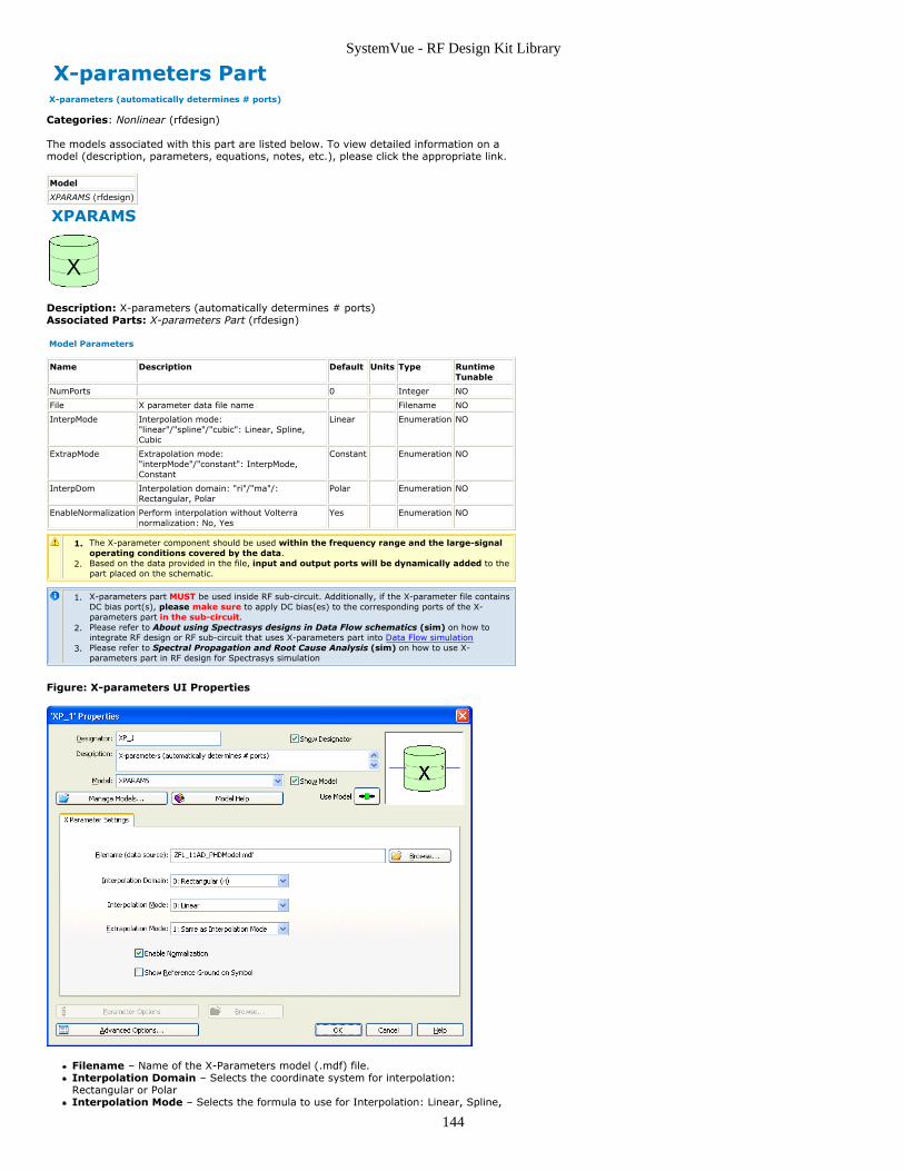
SystemVue - RF Design Kit Library
144
X-parameters Part X-parameters (automatically determines # ports)
Categories: Nonlinear (rfdesign)
The models associated with this part are listed below. To view detailed information on amodel (description, parameters, equations, notes, etc.), please click the appropriate link.
Model
XPARAMS (rfdesign)
XPARAMS
Description: X-parameters (automatically determines # ports)Associated Parts: X-parameters Part (rfdesign)
Model Parameters
Name Description Default Units Type RuntimeTunable
NumPorts 0 Integer NO
File X parameter data file name Filename NO
InterpMode Interpolation mode:"linear"/"spline"/"cubic": Linear, Spline,Cubic
Linear Enumeration NO
ExtrapMode Extrapolation mode:"interpMode"/"constant": InterpMode,Constant
Constant Enumeration NO
InterpDom Interpolation domain: "ri"/"ma"/:Rectangular, Polar
Polar Enumeration NO
EnableNormalization Perform interpolation without Volterranormalization: No, Yes
Yes Enumeration NO
The X-parameter component should be used within the frequency range and the large-signal1.operating conditions covered by the data.Based on the data provided in the file, input and output ports will be dynamically added to the2.part placed on the schematic.
X-parameters part MUST be used inside RF sub-circuit. Additionally, if the X-parameter file contains1.DC bias port(s), please make sure to apply DC bias(es) to the corresponding ports of the X-parameters part in the sub-circuit.Please refer to About using Spectrasys designs in Data Flow schematics (sim) on how to2.integrate RF design or RF sub-circuit that uses X-parameters part into Data Flow simulationPlease refer to Spectral Propagation and Root Cause Analysis (sim) on how to use X-3.parameters part in RF design for Spectrasys simulation
Figure: X-parameters UI Properties
Filename – Name of the X-Parameters model (.mdf) file.Interpolation Domain – Selects the coordinate system for interpolation:Rectangular or PolarInterpolation Mode – Selects the formula to use for Interpolation: Linear, Spline,

SystemVue - RF Design Kit Library
145
or Cubic.Extrapolation Mode – Either Constant or use the current Iterpolation Mode.Enable Normalization – When checked, interpolation is performed with Volterranormalization.Show Reference Ground – When checked, an alternate symbol is used with aReference Ground on the bottom edge, as shown below:
NoteWhen an X-Params model is placed the schematic symbol contains no pins. This is because the X-parameter file has not yet been selected (and of course, has not been read); the number of ports cannotbe determined until the file is actually read (via the Browse button).
The X-Parameters symbol is based on the .mdf file. After a Browse operation, the numberof ports will be automatically adjusted. In addition, "special" ports are indicated withdistinctive colors: VDC ports are drawn in aqua and marked with a dot; IDC ports areorange and also marked with a dot. An example follows:
Also, one or two additional (optional) tab pages may appear (after a Browse): A UserParameters tab may appear, if the X-parameter file has any User Variables defined.
These optional parameters are defined by the file. You may NOT add, delete, or renamethe User Variables, but you can change their values to any floating point number.(Equations are not permitted for values.)
NoteThe Min and Max values are NOT hard limits. They indicate the range specified by the X-Parameters .mdffile. If you use a number outside of the range, the data will be extrapolated and the results may not be asaccurate as a value within the range.
A Details page displays a summary of the info from the X-Paramters .mdf file.
Notes/Equations
The X-parameters part facilitates simulation of behavioral models described in terms1.of n-port X-parameter data.The data file needs to contain X-parameters data for an n-port device.2.Data files must be of GMDIF type and can be generated using either Agilent ADS SW3.or the Agilent NVNA instrument. Version 2.0 X-parameter GMDIF files as well asearlier versions produced by NVNA are supported.For information on GMDIF data file format, refer to X-parameter GMDIF Format4.(users).The X-parameters part uses tabular data and, therefore, its simulation inherently5.involves interpolation. The Interpolation Mode parameter selects the interpolationtechnique to be applied to the data. The Linear mode is the fastest and in most casesprovides sufficiently good results.The Interpolation Domain parameter refers to how complex data is interpolated6.and has two settings:
Rectangular mode: provide good results for most applications andPolar (default) mode: is a better choice for frequency sweeps.
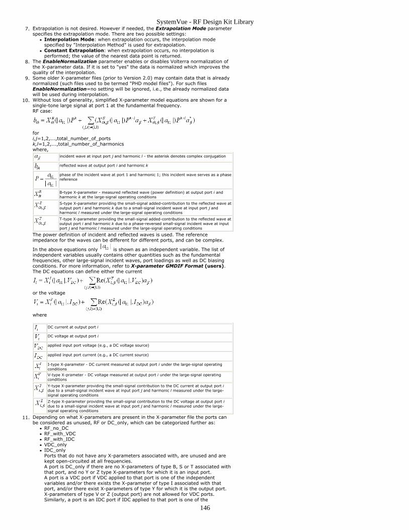
SystemVue - RF Design Kit Library
146
Extrapolation is not desired. However if needed, the Extrapolation Mode parameter7.specifies the extrapolation mode. There are two possible settings:
Interpolation Mode: when extrapolation occurs, the interpolation modespecified by "Interpolation Method" is used for extrapolation.Constant Extrapolation: when extrapolation occurs, no interpolation isperformed; the value of the nearest data point is returned.
The EnableNormalization parameter enables or disables Volterra normalization of8.the X-parameter data. If it is set to "yes" the data is normalized which improves thequality of the interpolation.Some older X-parameter files (prior to Version 2.0) may contain data that is already9.normalized (such files used to be termed "PHD model files"). For such filesEnableNormalization=no setting will be ignored, i.e., the already normalized datawill be used during interpolation.Without loss of generality, simplified X-parameter model equations are shown for a10.single-tone large signal at port 1 at the fundamental frequency.RF case:
fori,j=1,2,...,total_number_of_portsk,l=1,2,...,total_number_of_harmonicswhere,
incident wave at input port j and harmonic l - the asterisk denotes complex conjugation
reflected wave at output port i and harmonic k
phase of the incident wave at port 1 and harmonic 1; this incident wave serves as a phasereference
B-type X-parameter - measured reflected wave (power definition) at output port i andharmonic k at the large-signal operating conditions
S-type X-parameter providing the small-signal added-contribution to the reflected wave atoutput port i and harmonic k due to a small-signal incident wave at input port j andharmonic l measured under the large-signal operating conditions
T-type X-parameter providing the small-signal added-contribution to the reflected wave atoutput port i and harmonic k due to a phase-reversed small-signal incident wave at inputport j and harmonic l measured under the large-signal operating conditions
The power definition of incident and reflected waves is used. The referenceimpedance for the waves can be different for different ports, and can be complex.
In the above equations only is shown as an independent variable. The list ofindependent variables usually contains other quantities such as the fundamentalfrequencies, other large-signal incident waves, port loadings as well as DC biasingconditions. For more information, refer to X-parameter GMDIF Format (users).The DC equations can define either the current
or the voltage
where
DC current at output port i
DC voltage at output port i
applied input port voltage (e.g., a DC voltage source)
applied input port current (e.g., a DC current source)
I-type X-parameter - DC current measured at output port i under the large-signal operatingconditions
V-type X-prameter - DC voltage measured at output port i under the large-signal operatingconditions
Y-type X-parameter providing the small-signal contribution to the DC current at output port idue to a small-signal incident wave at input port j and harmonic l measured under the large-signal operating conditions
Z-type X-parameter providing the small-signal contribution to the DC voltage at output port idue to a small-signal incident wave at input port j and harmonic l measured under the large-signal operating conditions
Depending on what X-parameters are present in the X-parameter file the ports can11.be considered as unused, RF or DC_only, which can be categorized further as:
RF_no_DCRF_with_VDCRF_with_IDCVDC_onlyIDC_onlyPorts that do not have any X-parameters associated with, are unused and arekept open-circuited at all frequencies.A port is DC_only if there are no X-parameters of type B, S or T associated withthat port, and no Y or Z type X-parameters for which it is an input port.A port is a VDC port if VDC applied to that port is one of the independentvariables and/or there exists the X-parameter of type I associated with thatport, and/or there exist X-parameters of type Y for which it is the output port.X-parameters of type V or Z (output port) are not allowed for VDC ports.Similarly, a port is an IDC port if IDC applied to that port is one of the

SystemVue - RF Design Kit Library
147
independent variables and/or there exists the X-parameter of type V associatedwith that port, and/or there exist X-parameters of type Z for which it is theoutput port. X-parameters of type I or Y (output port) are not allowed for IDCports.VDC_only ports are kept open-circuited at all non-zero frequencies.IDC_only ports are kept short-circuited at all non-zero frequencies.RF ports are matched at all frequencies for which there are no X-parametersassociated with.RF_only ports are short-circuited at DC.
This component does not generate any noise.12.
References
D. E. Root et al., "Broad-Band Poly-Harmonic Distortion (PHD) Behavioral Models1.From Fast Automated Simulations and Large-Signal Vectorial NetworkMeasurements," IEEE Trans. MTT, vol. 53, no. 11, pp. 3656-3664, November 2005.J. Verspecht and D. E. Root, "Poly-Harmonic Distortion Modeling," IEEE Microwave2.Theory and Techniques Microwave Magazine, pp. 44-57, June, 2006.J. Verspecht, D. Gunyan, J. Horn, J. Xu, A. Cognata, and D.E. Root, "Multi-tone,3.Multi-Port, and Dynamic Memory Enhancements to PHD Nonlinear Behavioral Modelsfrom Large-Signal Measurements and Simulations," 2007 IEEE MTT-S Int. MicrowaveSymp. Dig., (Honolulu, HI), pp. 969-972, June 2007.J. Horn et al., "X-parameter Measurement and Simulation of a GSM Handset4.Amplifier", Proc. 3rd European Microwave Integrated Circuits Conf., (Amsterdam, TheNetherlands), pp. 135-138, October 2008.

SystemVue - RF Design Kit Library
148
Resistor Part This is an ideal non-inductive resistor model.
Categories: Ideal (rfdesign), Lumped (rfdesign), Resistors (rfdesign)
The models associated with this part are listed below. To view detailed information on amodel (description, parameters, equations, notes, etc.), please click the appropriate link.
Model
RES (rfdesign)
Resistor (RES)
Lumped resistance. Like many common parts, a short version of the symbol is available byholding the SHIFT key down while placing the part.
Note: Use the keyboard shortcut key "R" to place a resistor in the schematic editor.
Description: Subcircuit (N-Port w/NET2)Associated Parts: Resistor Part (rfdesign), Subcircuit (w 2-PortNoGnd) Part (rfdesign),Subcircuit (w NET2) Part (rfdesign)
Model Parameters
Name Description Default Units Type Runtime Tunable
R Resistance 50 ohm Integer NO
Additional Parameters
Resistance (ohms) Specifies the value of the resistor in ohms.
SystemVue - RF Design Kit Library
149
ADC (Basic) Part Basic ADC using datasheet SNR
Categories: System (rfdesign)
The models associated with this part are listed below. To view detailed information on amodel (description, parameters, equations, notes, etc.), please click the appropriate link.
Model
ADC_BASIC (rfdesign)
ADC_BASIC
Description: Basic ADC using datasheet SNRAssociated Parts: ADC (Basic) Part (rfdesign)
Model Parameters
Name Description Default Units Type Runtime Tunable
Bits Number of bits 12 Integer NO
FS Sampling frequency 40 MHz Integer NO
Vrange Analog input voltagerange
2 V Integer NO
SNR Signal to Noise Ratio 70 dBFS Integer NO
Rin Input resistance 200 ohm Integer NO
Cin Input capacitance 5 pF Integer NO
This part is used to model the effects of analog to digital conversion on the RF path. Thisoutput from this model is analog rather than a digital binary output. This model can reallybe thought of as a non-ideal ADC followed by an ideal DAC so we have analog output. Theoutput spectrum is a continuous frequency spectrum representing the 1st Nyquist zone (0to Sample Rate / 2 Hz). All input spectrum will be aliased into the 1st Nyquist zone. TheSignal to Noise Ratio (SNR) is used to determine the effective noise figure contribution ofthe ADC. A good reference on ADC basics can be found in application note, "Basics ofDesigning a Digital Radio Receiver (Radio 101)", Brad Brannon, Analog Devices, Inc.
NOTE: The port on the ADC output should have the same impedance as the ADC to eliminate impedancemismatch effects on the data.
Additional Parameter Information
Number of Bits This is the number of bits used by the ADC. The theoretical SNR = Number of Bits x 6 dB.
SamplingFrequency
This the frequency at which the ADC is sampled. The Nyquist frequency = SamplingFrequency / 2. This model assumes that the external clock is ideal and does not affect theSNR. For non-ideal clocks include the performance degradation in the SNR.
Analog InputVoltage Range
This the peak to peak input voltage range of the ADC. The full scale voltage is determinedfrom this parameter as Vrms full scale = Vrange / (2 * sqrt(2) ).
Signal to NoiseRatio
The signal to noise ratio of the ADC is specified relative to the full scale rms voltage of theADC. NOTE: When examining the performance of an ADC in SPECTRASYS the carrier to noiseratio of the simulation and ADC will only be equivalent when there are no other alias signalsthat fall within the channel and the peak signal value is equivalent to the full scale voltage ofthe ADC.
InputResistance
This is the input resistance of the ADC.
InputCapacitance
This is the shunt input capacitance of the ADC.
Additional Operation Information
Noise Figure
The noise figure of the ADC is determined according to the following formula.NF (dB) = Full Scale Pin (dBm) - SNR (dB) - 10 Log ( FS / 2 ) - Thermal Noise Power(dBm/Hz)where Full Scale Pin (dBm) = 10 Log ( Vin^2 / Zin ) + 30 and Thermal Noise Power(dBm/Hz) = 10 Log ( kT ) + 30, Vin in rms, k is Boltzmann's constant and T istemperature in Kelvin
Broadband Input Noise
Broadband input noise from all Nyquist zones will be aliased into the ADC basebandoutput. Consequently, the final noise figure of the ADC will be affected by the noisefiltering of the input signals and noise as in the real world. Note: If no filtering is providedahead of the ADC then the noise performance of the ADC can be affected by thebandwidth of the noise as defined by the 'Ignore Frequency Above' and 'Ignore FrequencyBelow' parameters in the System Analysis since these limits determine the range ofbroadband noise.
Gain
This gain of the ADC is very close to 1 or 0 dB when the output is terminated in the sameresistance as the input resistance. When the input resistance is changed the ADC loadimpedance must also be changed to keep the gain at 0 dB.
Output Impedance

SystemVue - RF Design Kit Library
150
It is assumed that the ADC is does not change impedance from input to output.Consequently, the load impedance should always be the same as the input resistance.
Spectrum Identification
SPECTRASYS will show ADC identification information for spectrums at the output of theADC. An example is given below. In the equation in [] brackets the 'Nyq:x' identifies theoriginating Nyquist zone. In this example the 'Source' signal came from the 3rd Nyquistzone. A + or - sign will appear before the Nyquist zone indicator to identify invertedaliased spectrum. In this case the spectrum originated in an odd Nyquist zone so there isno spectrum inversion. The parts after the equation indicate the path the signal took toget to the ADC output.
Some ADC Basics
Nyquist requires that signal be sampled at twice the bandwidth of the signal. Therefore, ifthe signal bandwidth is 1 MHz, then sampling at 2 MHz is sufficient. Anything beyond thisis called Over Sampling. Under sampling is the act of sampling at a frequency much lessthan half of the actual signal frequency. Consequently, it is possible to both over sampleand under sample at the same time since one is defined with respect to the bandwidthand the other at the desired frequency.
The faster a signal is sampled, the larger the signal to noise ratio and lower the noise floorbecause the noise is spread over more frequencies. The signal to noise ratio (referencedto the full scale value of the ADC) is:
S/N (dBFS) = 6.02 * Bits + 1.76 + 10 Log ( Fsample rate / 2 )
Each time the sample rate is doubled the signal to noise ratio improves by 3 dB. Sincedigital filtering removes unwanted noise and spurious signals the SNR of the ADC may begreatly improved by filtering just the bandwidth of the desired signal. Therefore, the SNRis proportional to 10 Log ( Fsample rate / Filter BW ). The greater the ratio betweensample rate and filter bandwidth the higher the SNR.
Analog input ranges are divided up into Nyquist zones. The most common is the firstNyquist zone which goes from DC to one half the sampling frequency (FS). The 2ndNyquist zone is from FS / 2 to FS, 3rd is from FS to 3 FS / 2, etc., etc. A unique and usefuleffect of using higher Nyquist zones is that signals sampled in higher zones are mirroreddown to the first Nyquist zone once digitized. When input signals appearing in evenNyquist zones are down converted they are spectrally inverted.
DC Block
DC is not blocked.
Only the linear portion of this model is used by simulators other than Spectrasys.

SystemVue - RF Design Kit Library
151
Antenna Path Part Antenna Path
Categories: System (rfdesign)
The models associated with this part are listed below. To view detailed information on amodel (description, parameters, equations, notes, etc.), please click the appropriate link.
Model
PATH (rfdesign)
PATH
Description: Antenna PathAssociated Parts: Antenna Path Part (rfdesign)
Model Parameters
Name Description Default Units Type Runtime Tunable
G1 Gain of Antenna #1 0 dB Integer NO
G2 Gain of Antenna #2 0 dB Integer NO
Lossa Loss in db/decade 40 dB Integer NO
Lossb Loss at unit distance 100 dB Integer NO
DIST Distance 1 Integer NO
Loss1 Fixed Loss #1 0 dB Integer NO
Loss2 Fixed Loss #2 0 dB Integer NO
ZIN Input Impedance 50 ohm None NO
ZOUT Output Impedance 50 ohm None NO
This part is used to provide antenna gains and path losses for a pair of antennas.
Additional Parameter/Operation Information
The coupled antenna gains and path losses are assumed to be constant acrossfrequency. The total path loss is computed as:Total Loss = Lossb + [Lossa * log 10 (DIST)] -G1 - G2 + Loss1 + Loss2
The units for distance is arbitrary. However 'Lossa' is the rate of the attenuation forthe same distance unit. Therefore, if the distance is in miles then 'Lossa' must be theattenuation in dB per mile.
NoteThe antenna gains should be positive. The losses must also be positive. The input and output impedancesmust be non-zero.

SystemVue - RF Design Kit Library
152
Attenuator (DC Control) Part Attenuator
Categories: System (rfdesign)
The models associated with this part are listed below. To view detailed information on amodel (description, parameters, equations, notes, etc.), please click the appropriate link.
Model
ATTN_Ctrl (rfdesign)
ATTN_Ctrl
Description: AttenuatorAssociated Parts: Attenuator (DC Control) Part (rfdesign)
Model Parameters
Name Description Default Units Type Runtime Tunable
ILVmax Loss at maximum voltage -50.0 dB Integer NO
ILVmin Loss at minimum voltage 0.0 dB Integer NO
Vmin Minimum voltage 0 V None NO
Slope Gain slope (dB/V) -10.0 None NO
ZIN Input Impedance 50 ohm None NO
ZOUT Output Impedance 50 ohm None NO
This part is used to provide attenuation in the RF path. The return loss of an RF attenuatoris double the total attenuation. Input and output impedances can be specified by theuser. The output impedance defaults to the input impedance unless otherwise specified bythe user. The attenuation in this model is constant across frequency.
Additional Parameter Information
Attenuation Assumed to be constant across frequency. For attenuation that varies with frequency use thefrequency dependent attenuator model.
Additional Operation Information
The non-linear model for this attenuator can be thought of as an internal amplifier with 0dB gain being connected to the output pin. The non-linear input parameters aretranslated to output parameters through the attenuation. For example, an input P1dB of -10 dBm will translated to an output P1dB of -13 for a total attenuation of 3 dB.
The attenuation of this device does not change as this device is driven into compression. Currently, the non-linear parameters are used to create intermods and harmonics. Thenoise figure of this device will also be independent of drive level.
Note: As the ratio of Zin to Zout gets very large or very small the input and output impedances will affectthe total insertion loss of the attenuator.
DC Block- DC is NOT blocked.
Only the linear portion of this model is used by simulators other than Spectrasys.

SystemVue - RF Design Kit Library
153
Attenuator (Frequency) Part Attenuator - Frequency Dependent
Categories: System (rfdesign)
The models associated with this part are listed below. To view detailed information on amodel (description, parameters, equations, notes, etc.), please click the appropriate link.
Model
AttnFreq (rfdesign)
ATTN_Linear (rfdesign)
ATTN_NonLinear (rfdesign)
SDATA_NL (rfdesign)
AttnFreq
Description: Attenuator - Frequency DependentAssociated Parts: Attenuator Part (rfdesign), Attenuator(Variable) Part (rfdesign),Attenuator (Frequency) Part (rfdesign)
Model Parameters
Name Description Default Units Type Runtime Tunable
LossList Attenuation List [50;1;1;30;30;40] dB Integer NO
FreqList Frequency List [98.9;99;101;101;102;102] MHz Integer NO
Zin Input Impedance 50 ohm None NO
Zout Output Impedance 50 ohm None NO
This part is used to provide linear frequency dependent attenuation in the RF path. A listof frequencies and losses can be entered. These values exist in frequency loss pairs. Thereturn loss of an RF attenuator is double the total attenuation. Input and outputimpedances can be specified by the user. This part can be used to create ideal filtermasks.
Additional Parameter Information
LossList This is the list of attenuation values. Each loss value is paired with the corresponding entry in thefrequency list. The list is an array of semicolon separated values. The return loss is always doublethe total attenuation at that frequency.
FreqList This is the list of frequencies at which the attenuation changes. Each frequency valued is paired withthe corresponding entry in the attenuation list. The list is an array of semicolon separated values.
Note:As the ratio of Zin to Zout gets very large or very small the input and output impedances will affectthe total insertion loss of the attenuator.
Additional Operation Information
DC Block - DC is NOT blocked.
Only the linear portion of this model is used by HARBEC.
SystemVue - RF Design Kit Library
154
Attenuator(Variable) Part Attenuator - Variable
Categories: System (rfdesign)
The models associated with this part are listed below. To view detailed information on amodel (description, parameters, equations, notes, etc.), please click the appropriate link.
Model
ATTN_VAR_Linear (rfdesign)
ATTN_VAR_NonLinear (rfdesign)
AttnFreq (rfdesign)
SDATA_NL (rfdesign)
ATTN_VAR_Linear
Description: Attenuator - VariableAssociated Parts: Attenuator(Variable) Part (rfdesign)
Model Parameters
Name Description Default Units Type Runtime Tunable
L Loss 2 dB Integer NO
IL Insertion Loss 1 dB Integer NO
ZIN Input Impedance 50 ohm None NO
ZOUT Output Impedance 50 ohm None NO
This part is used to provide variable attenuation in the RF path. The return loss of an RFattenuator is double the total attenuation. Input and output impedances can be specifiedby the user. The output impedance defaults to the input impedance unless otherwisespecified by the user. This part allows the user to separate the insertion loss from theattenuation and provides an appropriate schematic. The attenuation in this model isconstant across frequency.
Additional Operation Information
The total attenuation of the variable attenuator is simply the insertion loss plus theattenuation. Insertion Loss and Attenuation is assumed to be constant across frequency. For Insertion Loss and Attenuation that vary with frequency a post-processed equationcan be created.
The non-linear model for this attenuator can be thought of as an internal amplifier with 0dB gain being connected to the output pin. The non-linear input parameters aretranslated to output parameters through the insertion loss and attenuation. For example,an input P1dB of -10 dBm will translated to an output P1dB of -13 for a total attenuationof 3 dB.
The attenuation of this device does not change as this device is driven into compression.Currently, the non-linear parameters are used to create intermods and harmonics. Thenoise figure of this device will also be independent of drive level.
Note: As the ratio of Zin to Zout gets very large or very small the input and output impedances will affectthe total insertion loss of the attenuator.
DC Block -DC is NOT blocked.
Only the linear portion of this model is used by simulators other than Spectrasys.
ATTN_VAR_NonLinear
Description: Attenuator - VariableAssociated Parts: Attenuator(Variable) Part (rfdesign)
Model Parameters
Name Description Default Units Type Runtime Tunable
L Loss 2 dB Integer NO
IL Insertion Loss 1 dB Integer NO
ZIN Input Impedance 50 ohm None NO
ZOUT Output Impedance 50 ohm None NO
IP1dB Input P1dB 60.0 dBm None NO
IPSAT Input Saturation Power 63.0 dBm None NO
IIP3 Input IP3 70.0 dBm None NO
IIP2 Input IP2 80.0 dBm None NO
Non Linear AttenuatorsOnly linear attenuators exist in the parts library. To use a non-linear attenuator place a linear attenuatorin the schematic and then change the name of the Model to 'ATTN_NonLinear' on the 'General' tab of thepart properties.

SystemVue - RF Design Kit Library
155
Additional Parameter Information
Attenuation Assumed to be constant across frequency. For attenuation that varies with frequency use thefrequency dependent attenuator model .
Additional Operation Information
The non-linear model for this attenuator is simply an RF amplifier with negative gainwhere the input nonlinear parameters of the attenuator are translated to outputparameters of the amplifier through the loss.
Note: If the input saturation is greater than about 9 dB above the input 1 dB compression point thesaturation power will be set to 3 dB above the 1 dB compression point.
Note: As the ratio of Zin to Zout gets very large or very small the input and output impedances will affectthe total insertion loss of the attenuator.
DC Block - DC is NOT blocked.Orders Generated by Non-linear Section - 2nd and 3rd
WARNINGOnly the linear portion of this model is used by simulators other than Spectrasys.
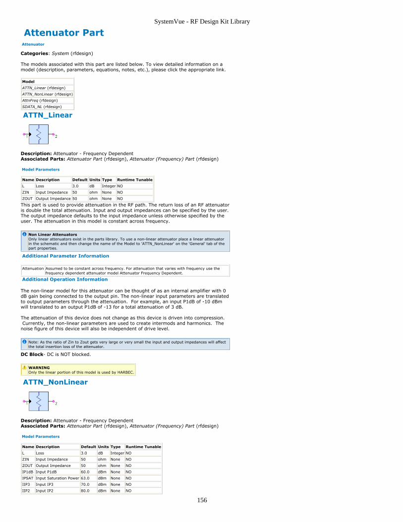
SystemVue - RF Design Kit Library
156
Attenuator Part Attenuator
Categories: System (rfdesign)
The models associated with this part are listed below. To view detailed information on amodel (description, parameters, equations, notes, etc.), please click the appropriate link.
Model
ATTN_Linear (rfdesign)
ATTN_NonLinear (rfdesign)
AttnFreq (rfdesign)
SDATA_NL (rfdesign)
ATTN_Linear
Description: Attenuator - Frequency DependentAssociated Parts: Attenuator Part (rfdesign), Attenuator (Frequency) Part (rfdesign)
Model Parameters
Name Description Default Units Type Runtime Tunable
L Loss 3.0 dB Integer NO
ZIN Input Impedance 50 ohm None NO
ZOUT Output Impedance 50 ohm None NO
This part is used to provide attenuation in the RF path. The return loss of an RF attenuatoris double the total attenuation. Input and output impedances can be specified by the user.The output impedance defaults to the input impedance unless otherwise specified by theuser. The attenuation in this model is constant across frequency.
Non Linear AttenuatorsOnly linear attenuators exist in the parts library. To use a non-linear attenuator place a linear attenuatorin the schematic and then change the name of the Model to 'ATTN_NonLinear' on the 'General' tab of thepart properties.
Additional Parameter Information
Attenuation Assumed to be constant across frequency. For attenuation that varies with frequency use thefrequency dependent attenuator model Attenuator Frequency Dependent.
Additional Operation Information
The non-linear model for this attenuator can be thought of as an internal amplifier with 0dB gain being connected to the output pin. The non-linear input parameters are translatedto output parameters through the attenuation. For example, an input P1dB of -10 dBmwill translated to an output P1dB of -13 for a total attenuation of 3 dB.
The attenuation of this device does not change as this device is driven into compression. Currently, the non-linear parameters are used to create intermods and harmonics. Thenoise figure of this device will also be independent of drive level.
Note: As the ratio of Zin to Zout gets very large or very small the input and output impedances will affectthe total insertion loss of the attenuator.
DC Block- DC is NOT blocked.
WARNINGOnly the linear portion of this model is used by HARBEC.
ATTN_NonLinear
Description: Attenuator - Frequency DependentAssociated Parts: Attenuator Part (rfdesign), Attenuator (Frequency) Part (rfdesign)
Model Parameters
Name Description Default Units Type Runtime Tunable
L Loss 3.0 dB Integer NO
ZIN Input Impedance 50 ohm None NO
ZOUT Output Impedance 50 ohm None NO
IP1dB Input P1dB 60.0 dBm None NO
IPSAT Input Saturation Power 63.0 dBm None NO
IIP3 Input IP3 70.0 dBm None NO
IIP2 Input IP2 80.0 dBm None NO

SystemVue - RF Design Kit Library
157
This part is used to provide attenuation in the RF path. The return loss of an RF attenuatoris double the total attenuation. Input and output impedances can be specified by theuser. The output impedance defaults to the input impedance unless otherwise specified bythe user. When the non-linear parameters are specified for this device Spectrasys willcreate intermods and harmonics based on these parameters. The linear simulator willignore all non-linear parameters. This model can be thought of as a linear attenuatorfollowed by a non-linear model that generates intermods and harmonics. The attenuationin this model is constant across frequency.
Non Linear AttenuatorsOnly linear attenuators exist in the parts library. To use a non-linear attenuator place a linear attenuatorin the schematic and then change the name of the Model to 'ATTN_NonLinear' on the 'General' tab of thepart properties.
Additional Parameter Information
Attenuation Assumed to be constant across frequency. For attenuation that varies with frequency use thefrequency dependent attenuator model .
Additional Operation Information
The non-linear model for this attenuator is simply an RF amplifier with negative gainwhere the input nonlinear parameters of the attenuator are translated to outputparameters of the amplifier through the loss.
Note: If the input saturation is greater than about 9 dB above the input 1 dB compression point thesaturation power will be set to 3 dB above the 1 dB compression point.
Note: As the ratio of Zin to Zout gets very large or very small the input and output impedances will affectthe total insertion loss of the attenuator.
DC Block - DC is NOT blocked.Orders Generated by Non-linear Section - 2nd and 3rd
WARNINGOnly the linear portion of this model is used by simulators other than Spectrasys.

SystemVue - RF Design Kit Library
158
Coupled Antenna Part Coupled Antenna
Categories: System (rfdesign)
The models associated with this part are listed below. To view detailed information on amodel (description, parameters, equations, notes, etc.), please click the appropriate link.
Model
AntCpld (rfdesign)
AntCpld
Description: Coupled AntennaAssociated Parts: Coupled Antenna Part (rfdesign)
Model Parameters
Name Description Default Units Type Runtime Tunable
Iso Isolation 30.0 dB Integer NO
Phase Phase lag 0 deg Float NO
ZIN Input Impedance 50 ohm None NO
ZOUT Output Impedance 50 ohm None NO
This part is used to provide a secondary RF output path from an antenna.
Additional Parameter/Operation Information
The coupled antenna isolation and phase are assumed to be constant acrossfrequency.
NoteThe isolation is an attenuation and must be positive. The phase is a lag and must also be positive. Theinput and output impedances must be non-zero.

SystemVue - RF Design Kit Library
159
Coupler(90 Deg Hybrid) Part 90 Degree Hybrid Coupler
Categories: System (rfdesign)
The models associated with this part are listed below. To view detailed information on amodel (description, parameters, equations, notes, etc.), please click the appropriate link.
Model
HYBRID1 (rfdesign)
HYBRID1
Description: 90 Degree Hybrid CouplerAssociated Parts: Coupler(90 Deg Hybrid) Part (rfdesign)
Model Parameters
Name Description Default Units Type Runtime Tunable
IL Insertion Loss 0.5 dB Integer NO
CPL Coupling 3.0103 dB Integer NO
ISO Isolation 40 dB Integer NO
GBAL Gain Balance 0 dB Integer NO
PBAL Phase Balance 0 deg Integer NO
ZIN1 Port 1 Input Impedance 50 ohm None NO
ZIN2 Port 2 Input Impedance 50 ohm None NO
ZIN3 Port 3 Input Impedance 50 ohm None NO
ZIN4 Port 4 Input Impedance 50 ohm None NO
This part is used to provide coupling in the RF path. The default is an equal power split (3dB) between the "direct" port (-90 degree) and the "coupled" port (0 degree). Both pathsare subject to the insertion loss.
Additional Parameter Information
InsertionLoss (IL)
Total Insertion Loss in dB (nodes 'In' to '0' and 'In' to '90', also for nodes 'Iso' to '0' and 'Iso' to'-90').
Coupling(CPL)
Coupling in dB (nodes 'In' to '0' and 'In' to '-90', default is 3.0103 dB). The gain balance at thecoupler output is dependent on the coupling. When the coupling is set to 3.0103 dB then thereis an equal amount of power at both coupler outputs.
Isolation(ISO)
Isolation in dB (nodes 'In' to 'Iso').
Gain Balance(GBAL)
Gain balance (gain difference between 0 degree and -90 degree paths, default is 0).
PhaseBalance(PBAL)
Phase balance (phase difference between 0 degree and -90 degree paths, default is 0).
Z0 Reference Impedance in ohms (default is 50 ohms).
Additional Operation Information
The gain balance error is equally divided between the direct and coupled paths.However, the phase balance is associated with the direct (-90 degree) path only. Theresulting s-parameters for the two paths are:
Gain (0 degree path) = { [ -IL (dB) ] + [ -CPL (dB) ] + [ 0.5 * GBAL (dB) ] } phase= 0 degreeGain (-90 degree path) = { [ -IL (dB) ] + [ -CPL (dB) ] + [- 0.5 * GBAL (dB) ] } phase = -90 degree - PBAL degree
Note: The coupling must always be greater than the insertion loss. If not, an error message will beprovided. In addition, a warning is supplied if the gain balance is greater than the coupling.
DC Block - DC is NOT blocked between the IN and 0 ports but is blocked for otherpaths.

SystemVue - RF Design Kit Library
160
Coupler(180 Deg Hybrid) Part 180 Degree Hybrid Coupler
Categories: System (rfdesign)
The models associated with this part are listed below. To view detailed information on amodel (description, parameters, equations, notes, etc.), please click the appropriate link.
Model
HYBRID180 (rfdesign)
HYBRID180
Description: 180 Degree Hybrid CouplerAssociated Parts: Coupler(180 Deg Hybrid) Part (rfdesign)
Model Parameters
Name Description Default Units Type Runtime Tunable
IL Insertion Loss 0.5 dB Integer NO
CPL Coupling 3.0103 dB Integer NO
ISO Isolation 40 dB Integer NO
GBAL Gain Balance 0 dB Integer NO
PBAL Phase Balance 0 deg Integer NO
ZIN1 Port 1 Input Impedance 50 ohm None NO
ZIN2 Port 2 Input Impedance 50 ohm None NO
ZIN3 Port 3 Input Impedance 50 ohm None NO
ZIN4 Port 4 Input Impedance 50 ohm None NO
This part is used to provide coupling in the RF path. The default is an equal power split (3db) between the "direct" port (-180 deg) and the "coupled" port (0 deg). Both paths aresubject to the insertion loss.
Additional Parameter Information
InsertionLoss (IL)
Total Insertion Loss in dB (nodes 'In' to '0' and 'In' to '-180', also for nodes 'Iso' to '0' and 'Iso'to '-180').
Coupling(CPL)
Coupling in dB (nodes 'In' to '0' and 'In' to '-180', default is 3.0103 dB). The gain balance atthe coupler output is dependent on the coupling. When the coupling is set to 3.0103 dB thenthere is an equal amount of power at both coupler outputs.
Isolation(ISO)
Isolation in dB (nodes 'In' to 'Iso').
Gain Balance(GBAL)
Gain balance (gain difference between 0 degree and -180 degree paths, default is 0).
PhaseBalance(PBAL)
Phase balance (phase difference between 0 degree and -180 degree paths, default is 0).
Z0 Reference Impedance in ohms (default is 50 ohms).
Additional Operation Information
The gain balance error is equally divided between the direct and coupled paths.However, the phase balance is associated with the direct (-180 degree) path only.The resulting s-parameters for the two paths are:Gain (0 degree path) = { [ -IL (dB) ] + [ -CPL (dB) ] + [ 0.5 * GBAL (dB) ] } phase= 0 degreeGain (-180 degree path) = { [ -IL (dB) ] + [ -CPL (dB) ] + [- 0.5 * GBAL (dB) ] } phase = -180 degree - PBAL degree
Note: The coupling must always be greater than the insertion loss. If not, an error message will beprovided. In addition, a warning is supplied if the gain balance is greater than the coupling.
DC Block - DC is NOT blocked between the IN and 0 ports but is blocked for otherpaths.

SystemVue - RF Design Kit Library
161
Coupler(Dual Dir) Part Dual Directional Coupler
Categories: System (rfdesign)
The models associated with this part are listed below. To view detailed information on amodel (description, parameters, equations, notes, etc.), please click the appropriate link.
Model
COUPLER2 (rfdesign)
COUPLER2
Description: Dual Directional CouplerAssociated Parts: Coupler(Dual Dir) Part (rfdesign)
Model Parameters
Name Description Default Units Type Runtime Tunable
IL Total Insertion Loss 0.5 dB Integer NO
CPL1 Coupling, Port 1 20.0 dB Integer NO
CPL2 Coupling, Port 2 20.0 dB Integer NO
DIR1 Directivity, Port 1 30.0 dB None NO
DIR2 Directivity, Port 2 30.0 dB None NO
ZIN1 Port 1 Input Impedance 50.0 ohm None NO
ZIN2 Port 2 Input Impedance 50.0 ohm None NO
ZIN3 Port 3 Input Impedance 50.0 ohm None NO
ZIN4 Port 4 Input Impedance 50.0 ohm None NO
This part is used to provide coupling in the RF path.
Additional Parameters/Operation Information
The coupler isolation (nodes 2 to 3 and 1 to 4) is equal to the coupling + directivity .Insertion Loss, Coupling, and Directivity is assumed to be constant across frequency.
Note: The total insertion loss of the coupler includes components due to attenuation and due to coupling.A warning is given if the specified "Total Insertion Loss" is less than the minimum theoretical loss due tocoupling. This minimum amount equals: {-10 log [ 1 - 10_CPL * 0.1^ ] } dB. When this occurs the totalinsertion loss of the coupler will be higher than the specified value.
DC Block - DC is NOT blocked for insertion path but is blocked for coupled paths.

SystemVue - RF Design Kit Library
162
Coupler(Single Dir) Part Single Directional Coupler
Categories: System (rfdesign)
The models associated with this part are listed below. To view detailed information on amodel (description, parameters, equations, notes, etc.), please click the appropriate link.
Model
COUPLER1 (rfdesign)
COUPLER1
Description: Single Directional CouplerAssociated Parts: Coupler(Single Dir) Part (rfdesign)
Model Parameters
Name Description Default Units Type Runtime Tunable
IL Total Insertion Loss 0.5 dB Integer NO
CPL Coupling 20.0 dB Integer NO
DIR Directivity 30.0 dB Integer NO
ZIN1 Port 1 Input Impedance 50.0 ohm None NO
ZIN2 Port 2 Input Impedance 50.0 ohm None NO
ZIN3 Port 3 Input Impedance 50.0 ohm None NO
This part is used to provide coupling in the RF path.
Additional Parameter/Operation Information
The coupler isolation (nodes 2 to 3) is equal to the coupling + directivity . InsertionLoss, Coupling, and Directivity is assumed to be constant across frequency.
Note: The total insertion loss of the coupler includes components due to attenuation and due to coupling.A warning is given if the specified "Total Insertion Loss" is less than the minimum theoretical loss due tocoupling. This minimum amount equals: {-10 log [ 1 - 10_CPL * 0.1^ ] } dB. When this occurs the totalinsertion loss of the coupler will be higher than the specified value.
DC Block - DC is NOT blocked for insertion path but is blocked for coupled path.

SystemVue - RF Design Kit Library
163
Digital Divider Part Digital Divider
Categories: System (rfdesign)
The models associated with this part are listed below. To view detailed information on amodel (description, parameters, equations, notes, etc.), please click the appropriate link.
Model
DIG_DIV (rfdesign)
DIG_DIV
Description: Digital DividerAssociated Parts: Digital Divider Part (rfdesign)
Model Parameters
Name Description Default Units Type Runtime Tunable
DIV Divider 2 Integer NO
DutyCycle Duty Cycle 0.5 Integer NO
InDrvMin Input Drive Level (Min) -15 dBm Integer NO
InDrvMax Input Drive Level (Max) 10.0 dBm Integer NO
OutLvl Output Level 5.0 dBm Integer NO
MinFundLvl Min Fundamental Output Level -15.0 dBm Integer NO
MinOutLvl Min Harmonic Output Level -10.0 dBm Integer NO
RISO Reverse Isolation 40.0 dB Integer NO
NOISE Output Noise Above Thermal 30.0 dB Integer NO
ScaleBW Scale Bandwidth (0-No, 1-Yes) 0 Integer NO
ZIN Input Impedance 50 ohm None NO
ZOUT Output Impedance 50 ohm None NO
This part is used to frequency divide input signals that fall within the input drivewindow. The divided output power level is constant whose power level is specified by theuser. This digital divider assumes that a duty cycle for the division ratio can be specified.From this assumed rectangular pulse duty cycle a Fourier series is used to determine theactual harmonic content of the divider output. In a real digital divider the rectangularpulse is not ideal so some additional parameters have been added to account for theseimperfections. These parameters are the minimum fundamental and harmonic outputlevels. No fundamental or harmonic output will ever fall below the power level specified bythese parameters even though their Fourier coefficients indicate the contrary. A goodexample of this is a duty cycle of 50%. In this case all even order products aretheoretically not present. However, in the real world this is not the case. In this case theminimum harmonic output level will control the output power level of the even orderharmonics.
All harmonics created by the divider (excluding the fundamental) appear back at the inputthrough the reverse isolation. These signals will then propagate backwards in a Spectrasyssimulation.
The number of harmonics created by this part is determined by the 'Maximum Order' and'Ignore Spectrum Frequency Above' parameters specified on the 'System Analysis' dialogbox. Once either one of these thresholds is reached no more harmonics will be created.
The bandwidth of all output signals will have the same bandwidth as the parent inputsignal.
In SPECTRASYS the 'Channel Frequency' will be divided by the divider value for theforward path. For example, the channel frequency at the divide by 8 input is 1 GHz thenthe output channel frequency will be 125 MHz. No channel frequency translation will occurfor reverse traveling signals.
All spectrum other than the single peak spectrum arriving at the input to this part will betreated as single sideband signals that will be decomposed into their AM and PMcomponents which will get processed by this frequency translation device. See the 'SSB toAM PM Decomposition' section for additional information.
Additional Parameter/Operation Information
Coherency
All signals created by the digital divider are assumed to be non-coherent with all othersignals and will create a new coherency identification number. The fundamental andreverse isolation signals are considered to be propagated and will maintain theircoherency identification number from their parent.
Examples
DIV=8 Dutycycle = 0.5 InDrvMin= -15 InDrvMax=10 OutLvl = 5 MinFundLvl = -40

SystemVue - RF Design Kit Library
164
MinOutLvl = -50 RISO=50 NOISE=23
This examples specifies a divide by 8 part with a 50% duty cycle. If the input frequency is1 GHz @ -10 dBm then several frequencies will be created at the output depending on the'Maximum Order' and 'Ignore Spectrum Frequency Above' parameters specified in theSystem Analysis. However, the 125 MHz signal (1 GHz / 8 ) will have a power level of +5dBm. All even harmonics will have a power level of -50 dBm since even harmonics aretheoretically non existent. Furthermore, since the fundamental or feedthrough signal (1GHz) is an even order (8th harmonic of the divided signal) and should also theoretically benon existent its power level will be -40 dBm. The noise floor output will be 23 dB abovethermal noise which is equivalent to a noise figure of 23 dB.
DC Block
DC is blocked.
WARNING: Only the linear portion of this model is used by simulators other than Spectrasys.

SystemVue - RF Design Kit Library
165
Duplexer(Chebyshev) Part Chebyshev Duplexer
Categories: System (rfdesign)
The models associated with this part are listed below. To view detailed information on amodel (description, parameters, equations, notes, etc.), please click the appropriate link.
Model
Duplexer_C (rfdesign)
Duplexer_C
Description: Chebyshev DuplexerAssociated Parts: Duplexer(Chebyshev) Part (rfdesign)
Model Parameters
Name Description Default Units Type Runtime Tunable
FLOA Lower Passband Edge Frequency, Part A 400 MHz Float NO
FHIA Higher Passband Edge Frequency, PartA
500 MHz Float NO
FLOB Lower Passband Edge Frequency, Part B 700 MHz Float NO
FHIB Higher Passband Edge Frequency, PartB
800 MHz Float NO
NA Filter Order, Part A (NA > 1) 3 none Float NO
NB Filter Order, Part B (NB > 1) 3 none Float NO
RA Ripple, Part A 0.5 dB Float NO
RB Ripple, Part B 0.5 dB Float NO
ILA Insertion Loss, Part A 1 dB Float NO
ILB Insertion Loss, Part B 1 dB Float NO
Apass Attenuation at Passband 3 dB Float NO
Amax Max Attenuation in Stopband 100 dB Float NO
Zin Input Impedance (Common Port) 50 ohm Float NO
Zout Ouput Impedance (Part A & B) 50 ohm Float NO
This part is used to provide a duplexer function in the RF path, made from two Chebyshevbandpass filters. The filters are marked "A" and "B" in the symbol.
Additional Parameter/Operation Information
The duplexer is a pair of filters with one common port. In this case the filters are ofthe Chebyshev type.The filter characteristic exhibits ripple in the passband andgenerated by poles only. Typically the value used for the attenuation at the passbandedge (Apass) is set equal to the ripple value. An alternative method of forming aduplexer is to use two separate filter parts and connecting them together in theschematic.
Note: The insertion loss and passband attenuation must be greater or equal to zero. The filter order mustbe an integer greater or equal to 2. The frequency of the passband edges must be positive and the higherfrequency must be larger than the lower frequency.
DC Block - DC is blocked.

SystemVue - RF Design Kit Library
166
Duplexer(Elliptic) Part Elliptic Duplexer
Categories: System (rfdesign)
The models associated with this part are listed below. To view detailed information on amodel (description, parameters, equations, notes, etc.), please click the appropriate link.
Model
Duplexer_E (rfdesign)
Duplexer_E
Description: Elliptic DuplexerAssociated Parts: Duplexer(Elliptic) Part (rfdesign)
Model Parameters
Name Description Default Units Type Runtime Tunable
FLOA Lower Passband Edge Frequency, Part A 400 MHz Float NO
FHIA Higher Passband Edge Frequency, PartA
500 MHz Float NO
FLOB Lower Passband Edge Frequency, Part B 700 MHz Float NO
FHIB Higher Passband Edge Frequency, PartB
800 MHz Float NO
NA Filter Order, Part A (NA > 1) 3 none Float NO
NB Filter Order, Part B (NB > 1) 3 none Float NO
RA Ripple, Part A 0.5 dB Float NO
RB Ripple, Part B 0.5 dB Float NO
ILA Insertion Loss, Part A 1 dB Float NO
ILB Insertion Loss, Part B 1 dB Float NO
SBAttn Stopband Attenuation 50 dB Float NO
AMAX Max Attenuation in Stopband 100 dB Float NO
Zin Input Impedance (Common Port) 50 ohm Float NO
Zout Output Impedance (Part A & B) 50 ohm Float NO
This part is used to provide a duplexer function in the RF path, made from two Ellipticbandpass filters. The filters are marked "A" and "B" in the symbol.
Additional Parameter/Operation Information
The duplexer is a pair of filters with one common port. In this case the filters are ofthe Elliptic type. The Elliptic filter characteristic exhibits ripple in the passband andgenerated by poles and zeros. This results in a cutoff which is sharper than mostother filters. An alternative method of forming a duplexer is to use two separate filterparts and connecting them together in the schematic.
Note: The insertion loss must be greater or equal to zero. The filter order must be an integer greater orequal to 2. The frequencies of the passband edges must be positive and the higher frequency must belarger than the lower frequency. The stopband attenuation must be greater than the ripple.
DC Block - DC is blocked.

SystemVue - RF Design Kit Library
167
Freq Divider Part Frequecy Divider
Categories: System (rfdesign)
The models associated with this part are listed below. To view detailed information on amodel (description, parameters, equations, notes, etc.), please click the appropriate link.
Model
FREQ_DIV (rfdesign)
FREQ_DIV
Description: Frequecy DividerAssociated Parts: Freq Divider Part (rfdesign)
Model Parameters
Name Description Default Units Type Runtime Tunable
CG Conversion Gain -10 dB Integer NO
MULT Multiplier 1 Integer NO
DIV Divider 2 Integer NO
HL Harmonics (f1;f2;...;fn) -10;0;-20;-30 dB Integer NO
InDrv Input Drive Level -10 dBm Integer NO
RISO Reverse Isolation 40 dB Integer NO
NOISE Output Noise Above Thermal none dB Integer NO
ScaleBW Scale Bandwidth (0-No, 1-Yes) 0 Integer NO
ZIN Input Impedance 50 ohm None NO
ZOUT Output Impedance 50 ohm None NO
This part is used to frequency divide input signals that exceed the input drive levelthreshold. This divider part internally includes both a frequency multiplier followed by afrequency divider. The will allow the maximum flexibility so the user can create a non-integer frequency multiplier and/or divider.
All spectrum other than the single peak spectrum arriving at the input to this part will betreated as single sideband signals that will be decomposed into their AM and PMcomponents which will get processed by this frequency translation device. See the 'SSB toAM PM Decomposition' section for additional information.
* For Linear operation, only these variables are used. The resulting s-parameters are: S 21
= CG dB, S 12 = -RISO dB, NF = Noise - CG .
Additional Parameter/Operation Information
About the Model
The frequency divider model internally is a frequency multiplier followed by a frequencydivider. The multiplier section operates just like frequency multiplier model (FREQ_MULT)followed by a frequency division. The 'Multiplier Value' specifies the desired harmonicnumber (default for the divider = 1) where the 'Conversion Gain' is the difference inpower between the input fundamental signal and the desired output harmonic level. The 'Harmonic Level' table specifies the amplitude of the fundamental signal and eachharmonic. The harmonic levels are in dBc relative to the desired harmonic output level. Consequently, there should be an entry in the table that contains 0 dBc for the desiredharmonic level. As expected the bandwidth of all harmonic signals at the output will bemultiplied by the respective harmonic (i.e. the 5th harmonic will have 5 times thebandwidth as the input signal). It is assumed that all entries in the harmonic level tablehave been measured in a bandwidth greater than or equal to the bandwidth of theharmonic. The 'Input Drive Level' is the target input power for the multiplier. Thisvalue is only used in the simulation to determine if the input power is out of range. The 'Range Tolerance' can be specified in the system simulation dialog box. Once allharmonics have been created as specified in the Harmonic Level Table they are followedby a frequency division as specified by the 'Divider Value'.
Harmonics
All harmonics created by the multiplier (excluding the fundamental) appear at the input ofthe multiplier through the reverse isolation. These signals will then propagate backwardsin a Spectrasys simulation.
The number of harmonics created by the multiplier is solely determined by the number ofentries in the harmonic level table (i.e. if there are 10 entries then 10 harmonics will becreated. The maximum number of harmonics must be less than 100.
Divider
All harmonics at the output are divided in frequency by the divider value. The amplitude ofeach divided harmonic is based on the values in the harmonic table.

SystemVue - RF Design Kit Library
168
Leakage
The leakage of the divider occurs at the frequency of the input. For example, if the inputfrequency is 100 MHz then the 2nd harmonic of a two way divider would also be 100 MHzso the 2nd entry in the harmonic table along with the conversion gain will be used todetermine the leakage value.
Channel Frequency
In Spectrasys the 'Channel Frequency' will be multiplied by the multiplier value only forthe forward path. No channel frequency translation will occur for reverse travelingsignals.
Coherency
All signals created by the frequency multiplier are assumed to be non-coherent with allother signals and will create a new coherency identification number. The fundamental andreverse isolation signals are considered to be propagated and will maintain theircoherency identification number from their parent.
Note: If the channel measurement bandwidth is narrower than the multiplied bandwidth the output powerfor that harmonic will appear to be lower than expected. This is because Spectrasys is a channel basedmeasurement tool. All spectrum plots will be scaled by the channel bandwidth and most measurementsonly show power within the defined channel. Remember to set the 'channel measurement bandwidth' to abandwidth greater than or equal to the largest measured harmonic.
Note: The default 'Ignore Spectrum Frequency Above' limit defaults to 5 times the highest inputfrequency. Please readjust this limit to include all of the desired harmonics of the multiplier.
Examples
FREQ_MULT 1 2 MULT =1 DIV=8 CG =-17 HL=0;20;23;15 InDrv=10 RISO=50 NOISE=23
This examples specifies a divide by 8 part with a 17 dB conversion loss. The fundamentalsignal at the output will be 15 dB below the 2nd harmonic. Likewise a 3rd and 4thharmonic will also be created that will be 23 dB and 15 dB respectively below the 2ndharmonic level. The target input drive level is +10 dBm. The noise floor output will be 23dB above thermal noise which is equivalent to a noise figure of 40 dB (23 dB noise - ( -17)conversion gain). If the system analysis range tolerance is 2 dB then a warning willappear if the total input drive level is less than +8 dBm or greater than +12 dBm.
If the input frequency is 1 GHz @ +10 dBm then four frequencies and their power levelsappearing at the output would be 125 MHz @ -7 dBm, 250 MHz @ -27 dBm, 375 MHz @ -30 dBm, and 500 MHz @ -22 dBm.
DC Block
DC is blocked.
WARNING: Only the linear portion of this model is used by simulators other than Spectrasys.

SystemVue - RF Design Kit Library
169
Freq Multiplier Part Frequecy Multiplier
Categories: System (rfdesign)
The models associated with this part are listed below. To view detailed information on amodel (description, parameters, equations, notes, etc.), please click the appropriate link.
Model
FREQ_MULT (rfdesign)
FREQ_MULT
Description: Frequecy MultiplierAssociated Parts: Freq Multiplier Part (rfdesign)
Model Parameters
Name Description Default Units Type Runtime Tunable
CG Conversion Gain -20 dB Integer NO
MULT Multiplier 2 Integer NO
HL Harmonics (f1;f2;...;fn) -10;0;-20;-30 dB Integer NO
InDrv Input Drive Level -10 dBm Integer NO
RISO Reverse Isolation 50 dB Integer NO
NOISE Output Noise Above Thermal 20 dB Integer NO
ScaleBW Scale Bandwidth (0-No, 1-Yes) 0 Integer NO
ZIN Input Impedance 50 ohm None NO
ZOUT Output Impedance 50 ohm None NO
This part is used to frequency multiply input signals that exceed the input drive levelthreshold. The user can specify up to 100 harmonics that can be created by the multiplier.
All spectrum other than the single peak spectrum arriving at the input to this part will betreated as single sideband signals that will be decomposed into their AM and PMcomponents which will get processed by this frequency translation device. See the 'SSB toAM PM Decomposition' section for additional information.
* For Linear operation, only these variables are used. The resulting s-parameters are: S 21
= CG dB, S 12 = -RISO dB, NF = Noise - CG .
Additional Parameter/Operation Information
Frequency Multiplier
The frequency multiplier models can create up to 100 harmonics at its output. The 'Multiplier Value' specifies the desired harmonic number where the 'Conversion Gain' isthe difference in power between the input fundamental signal and the desired outputharmonic level. The 'Harmonic Level' table specifies the amplitude of the fundamentalsignal and each harmonic. The harmonic levels are in dBc relative to the desired harmonicoutput level. Consequently, there should be an entry in the table that contains 0 dBc forthe desired harmonic level. As expected the bandwidth of all harmonic signals at theoutput will be multiplied by the respective harmonic (i.e. the 5th harmonic will have 5times the bandwidth as the input signal). It is assumed that all entries in the harmoniclevel table have been measured in a bandwidth greater than or equal to the bandwidth ofthe harmonic. The 'Input Drive Level' is the target input power for the multiplier. Thisvalue is only used in the simulation to determine if the input power is out of range. The 'Range Tolerance' can be specified in the system simulation dialog box.
All harmonics created by the multiplier (excluding the fundamental) appear at the input ofthe multiplier through the reverse isolation. These signals will then propagate backwardsin a Spectrasys simulation.
The number of harmonics created by the multiplier is solely determined by the number ofentries in the harmonic level table (i.e. if there are 10 entries then 10 harmonics will becreated. The maximum number of harmonics must be less than 100.
In Spectrasys the 'Channel Frequency' will be multiplied by the multiplier value only forthe forward path. No channel frequency translation will occur for reverse travelingsignals.
Coherency
All signals created by the frequency multiplier are assumed to be non-coherent with allother signals and will create a new coherency identification number. The fundamental andreverse isolation signals are considered to be propagated and will maintain theircoherency identification number from their parent.

SystemVue - RF Design Kit Library
170
Note: If the channel measurement bandwidth is narrower than the multiplied bandwidth the output powerfor that harmonic will appear to be lower than expected. This is because Spectrasys is a channel basedmeasurement tool. All spectrum plots will be scaled by the channel bandwidth and most measurementsonly show power within the defined channel. Remember to set the 'channel measurement bandwidth' to abandwidth greater than or equal to the largest measured harmonic.
Note: The default 'Ignore Spectrum Frequency Above' limit defaults to 5 times the highest inputfrequency. Please readjust this limit to include all of the desired harmonics of the multiplier.
Examples
FREQ_MULT 1 2 MULT =2 CG =-17 HL=15;0;23;15 InDrv=10 RISO=50 NOISE=23 This examples specifies a frequency doubler (multiplier = 2) with a 17 dB conversion loss.The fundamental signal at the output will be 15 dB below the 2nd harmonic. Likewise a3rd and 4th harmonic will also be created that will be 23 dB and 15 dB respectively belowthe 2nd harmonic level. The target input drive level is +10 dBm. The noise floor outputwill be 23 dB above thermal noise which is equivalent to a noise figure of 40 dB (23 dBnoise - ( -17) conversion gain). If the system analysis range tolerance is 2 dB then awarning will appear if the total input drive level is less than +8 dBm or greater than +12dBm.
If the input frequency is 1 GHz @ +10 dBm then four frequencies and their power levelsappearing at the output would be 1GHz @ -22 dBm, 2 GHz @ -7 dBm, 3 GHz @ -30 dBm,and 4 GHz @ -22 dBm.
DC Block
DC is blocked.
WARNING: Only the linear portion of this model is used by simulators other than Spectrasys.

SystemVue - RF Design Kit Library
171
Isolator Part Isolator
Categories: System (rfdesign)
The models associated with this part are listed below. To view detailed information on amodel (description, parameters, equations, notes, etc.), please click the appropriate link.
Model
ISO (rfdesign)
ISO
Description: IsolatorAssociated Parts: Isolator Part (rfdesign)
Model Parameters
Name Description Default Units Type Runtime Tunable
IL Insertion Loss 0.5 dB Integer NO
ISO Isolation 40 dB Integer NO
ZIN Input Impedance 50 ohm None NO
ZOUT Output Impedance 50 ohm None NO
Notes and Equations
Additional Parameter/Operation InformationThis part is used to provide directional control of signals in the RF path.
Insertion Loss, and Isolation is assumed to be constant across frequency.
Note: As the isolation is reduced to the point that it begins to approach the insertion loss the totalinsertion loss will no longer be the value specified by the user.
DC Block - DC is NOT blocked between ports.

SystemVue - RF Design Kit Library
172
Log Detector Part Log Detector
Categories: System (rfdesign)
The models associated with this part are listed below. To view detailed information on amodel (description, parameters, equations, notes, etc.), please click the appropriate link.
Model
LOG_DET (rfdesign)
LOG_DET
Description: Log DetectorAssociated Parts: Log Detector Part (rfdesign)
Model Parameters
Name Description Default Units Type Runtime Tunable
Slope Slope|v/dB 0.05 Integer NO
Intercept Power intercept -100 dBm Integer NO
Vmin Output threshold 0 V Integer NO
Vsat Outputsaturation
5 V Integer NO
Zin Input Impedance 50 ohm None NO
This part is used to provide a DC output voltage proportional to the total power appearingat the RF input port. The total input power includes all signals, intermods, and noise.
Additional Parameter Information
Slope This is the rate at which the output voltage will change per dB in total input power.
PowerIntercept
This is the total RF power level at which 0 Volts DC will be created at the output.
OuputThreshold
This is the minimum output voltage of the detector. If the output threshold is greater than 0Volts then the total RF input power will need to increase to the point when the DC output isgreater than this threshold.
OutputSaturation
This is the maximum output level of the detector.
InputImpedance
This is the nominal impedance of the detector.
Additional Operation Information
The transfer function of the log detector is as shown in the diagram below. The DC outputvoltage is proportional to the total RF signal power appearing at the detector input. Thismodel is frequency independent so all signal frequencies in the entire spectrum aretreated equally including noise power . To band limit the detector place a filter ahead ofthe detector.
The output impedance of the DC port is defined to be 1 Megohm.
The DC output voltage can be calculated as:
VDC at Output = (Total Node Power at Input - Power Intercept) * Slope.
If VDC is less than the Output Threshold the Output Threshold value will be used. Likewiseif VDC is greater than the Output Saturation then the Output Saturation value will beused.
Note: The detector input is broadband. There are no frequency limitations. Consequently the totalintegrated noise power may be much higher than anticipated. The 'Total Node Power' measurementrepresents the total power entering the log detector that will be converted to DC.

SystemVue - RF Design Kit Library
173
Splitter(2-Way 0 deg) Part 2 Way 0 Degree Splitter / Combiner
Categories: System (rfdesign)
The models associated with this part are listed below. To view detailed information on amodel (description, parameters, equations, notes, etc.), please click the appropriate link.
Model
SPLIT2 (rfdesign)
SPLIT2
Description: 2 Way 0 Degree Splitter / CombinerAssociated Parts: Splitter(2-Way 0 deg) Part (rfdesign)
Model Parameters
Name Description Default Units Type Runtime Tunable
IL Insertion Loss 3.02 dB Integer NO
ISO Isolation 30 dB Integer NO
PH2 Phase, port 2 -90 deg Float NO
GBal2 Gain Balance, port3
0 dB Float NO
PH3 Phase, port 3 -90 deg Float NO
Zin Input Impedance 50 ohm None NO
Zout Output Impedance 50 ohm None NO
This part is used to split or combine RF paths. The phase difference between the two splitpaths is 0 degrees.
Additional Parameter Information
Insertion loss, phase and isolation are assumed to be constant across frequency. Theminimum insertion loss of an ideal splitter is 10*Log(1/N) dB, where N is the number ofpaths. The gain balance error is assigned to the 1 -> 3 path only. However, the phasespecifications apply to each output with respect to the input. The resulting s-parametersfor the two paths are: S 21 = { [ -IL (db) ] } with phase = PH2 deg
S 31 = { [ -IL (db) ] + [ Gbal2 (db) ] } with phase = PH3 deg
The total loss of this device consists of 3 loss contributors: 1) division loss ( 10 Log 1/N,where N is the number split paths), 2) dissipative loss ( typically due to the Q of thecomponents and transmission line losses), and 3) isolation or coupling loss ( port-to-portisolations ). The insertion loss specified for this device must include all three of these lossparameters or the device will appear to be active. A warning will be given when thisoccurs. For example, in practice the user cannot expect to have an insertion loss ofaround 3 dB for a 2 way splitter if the port-to-port isolation is very low.
Additional Operation Information
DC Block - DC is NOT blocked for all paths.
Note: Phase for each path should be negative. The total output energy must not exceed the input energyor the device will appear to be active.

SystemVue - RF Design Kit Library
174
Splitter(2-way 90 deg) Part 2 Way 90 Degree Splitter / Combiner
Categories: System (rfdesign)
The models associated with this part are listed below. To view detailed information on amodel (description, parameters, equations, notes, etc.), please click the appropriate link.
Model
SPLIT290 (rfdesign)
SPLIT290
Description: 2 Way 90 Degree Splitter / CombinerAssociated Parts: Splitter(2-way 90 deg) Part (rfdesign)
Model Parameters
Name Description Default Units Type Runtime Tunable
IL Insertion Loss 3.02 dB Integer NO
ISO Isolation 30 dB Integer NO
PH2 Phase, port 2 0 deg Float NO
GBal2 Gain Balance, port3
0 dB Float NO
PH3 Phase, port 3 -90 deg Float NO
Zin Input Impedance 50 ohm None NO
Zout Output Impedance 50 ohm None NO
This part is used to split or combine RF paths. The phase difference between the two splitpaths is 90 degrees.
Additional Parameter Information
Insertion loss, phase and isolation are assumed to be constant across frequency. Theminimum insertion loss of an ideal splitter is 10*Log(1/N) dB, where N the number ofpaths. The gain balance error is added to path 1 ->3 only. However, the phasespecifications apply to each output with respect to the input. The resulting s-parametersfor the two paths are: S 21 = { [ -IL (db) ] } with phase = PH2 deg
S 31 = { [ -IL (db) ] + [Gbal2 (db) ] } with phase = PH3 deg
The total loss of this device consists of 3 loss contributors: 1) division loss ( 10 Log 1/N,where N is the number split paths), 2) dissipative loss ( typically due to the Q of thecomponents and transmission line losses), and 3) isolation or coupling loss ( port-to-portisolations ). The insertion loss specified for this device must include all three of these lossparameters or the device will appear to be active. A warning will be given when thisoccurs. For example, in practice the user cannot expect to have an insertion loss ofaround 3 dB for a 2 way splitter if the port-to-port isolation is very low.
Additional Operation Information
DC Block - DC is NOT blocked for all paths.
Note: Phase for each path should be negative. The total output energy must not exceed the input energyor the device will appear to be active.

SystemVue - RF Design Kit Library
175
Splitter(2-way 180 deg) Part 2 Way 180 Degree Splitter / Combiner
Categories: System (rfdesign)
The models associated with this part are listed below. To view detailed information on amodel (description, parameters, equations, notes, etc.), please click the appropriate link.
Model
SPLIT2180 (rfdesign)
SPLIT2180
Description: 2 Way 180 Degree Splitter / CombinerAssociated Parts: Splitter(2-way 180 deg) Part (rfdesign)
Model Parameters
Name Description Default Units Type Runtime Tunable
IL Insertion Loss 3.02 dB Integer NO
ISO Isolation 30 dB Integer NO
PH2 Phase, port 2 -90 deg Float NO
GBal2 Gain Balance, port3
0 dB Float NO
PH3 Phase, port 3 -270 deg Float NO
Zin Input Impedance 50 ohm None NO
Zout Output Impedance 50 ohm None NO
This part is used to split or combine RF paths. The phase difference between the two splitpaths is 180 degrees.
Additional Parameter Information
Insertion loss, phase and isolation are assumed to be constant across frequency. Theminimum insertion loss of an ideal splitter is 10*Log(1/N) dB, where N the number ofpaths. The gain balance error is added to path 1 ->3 only. However, the phasespecifications apply to each output with respect to the input. The resulting s-parametersfor the two paths are: S 21 = { [ -IL (db) ] } with phase = PH2 deg
S 31 = { [ -IL (db) ] + [Gbal2 (db) ] } with phase = PH3 deg
The total loss of this device consists of 3 loss contributors: 1) division loss ( 10 Log 1/N,where N is the number split paths), 2) dissipative loss ( typically due to the Q of thecomponents and transmission line losses), and 3) isolation or coupling loss ( port-to-portisolations ). The insertion loss specified for this device must include all three of these lossparameters or the device will appear to be active. A warning will be given when thisoccurs. For example, in practice the user cannot expect to have an insertion loss ofaround 3 dB for a 2 way splitter if the port-to-port isolation is very low.
Additional Operation Information
DC Block - DC is NOT blocked for all paths.
Note: Phase for each path should be negative. The total output energy must not exceed the input energyor the device will appear to be active.

SystemVue - RF Design Kit Library
176
Splitter(3-way 0 deg) Part 3 Way 0 Degree Splitter / Combiner
Categories: System (rfdesign)
The models associated with this part are listed below. To view detailed information on amodel (description, parameters, equations, notes, etc.), please click the appropriate link.
Model
SPLIT3 (rfdesign)
SPLIT3
Description: 3 Way 0 Degree Splitter / CombinerAssociated Parts: Splitter(3-way 0 deg) Part (rfdesign)
Model Parameters
Name Description Default Units Type Runtime Tunable
IL Insertion Loss 4.78 dB Integer NO
ISO Isolation 30 dB Integer NO
PH2 Phase, port 2 -90 deg Float NO
GBal2 Gain Balance, port3
0 dB Float NO
PH3 Phase, port 3 -90 deg Float NO
GBal3 Gain Balance, port4
0 dB Float NO
PH4 Phase, port 4 -90 deg Float NO
Zin Input Impedance 50 ohm None NO
Zout Output Impedance 50 ohm None NO
This part is used to split or combine RF paths. The phase difference between the N splitpaths is 0 degrees.
* where n is number of splits from 2 to 48
Note: Only a certain number of common splitters have been added to the parts list. To create a newsplitter part place an available splitter on the schematic and then change the name of the Model andSymbol on the 'General' tab of the part properties. i.e. a 7 way splitter will have a Model named 'SPLIT7'with a schematic Symbol called 'Split7'.
Additional Parameter Information
Insertion Loss (IL) The minimum insertion loss of an ideal splitter is 10 Log( n ) dB, where n thenumber of paths.
Gain Balance, port n(GBal<n-1>)
The gain balance error is the gain difference from the reference path. The referencepath is from the common port to port 2.
Phase Balance, port n(PH<n>)
The phase balance applies to each output with respect to the input.
Additional Operation Information
Frequency Response
Insertion loss, phase and isolation are assumed to be constant across frequency.
Losses
The total loss of this device consists of 3 loss contributors: 1) division loss ( 10 Log ( n ),where n is the number split paths), 2) dissipative loss ( typically due to the Q of thecomponents and transmission line losses), and 3) isolation or coupling loss ( port-to-portisolations ). The insertion loss specified for this device must include all three of these lossparameters or the device will appear to be active. A warning will be given when thisoccurs. For example, in practice the user cannot expect to have an insertion loss of around3 dB for a 2 way splitter if the port-to-port isolation is very low.
Note: Phase of each path should be negative. The total output energy must not exceed the input energyor the device will appear to be active.
DC Block
DC Block - DC is NOT blocked for all paths.
SystemVue - RF Design Kit Library
177
Splitter(4-way 0 deg) Part 4 Way 0 Degree Splitter / Combiner
Categories: System (rfdesign)
The models associated with this part are listed below. To view detailed information on amodel (description, parameters, equations, notes, etc.), please click the appropriate link.
Model
SPLIT4 (rfdesign)
SPLIT4
Description: 4 Way 0 Degree Splitter / CombinerAssociated Parts: Splitter(4-way 0 deg) Part (rfdesign)
Model Parameters
Name Description Default Units Type Runtime Tunable
IL Insertion Loss 6.05 dB Integer NO
ISO Isolation 30 dB Integer NO
PH2 Phase, port 2 -90 deg Float NO
GBal2 Gain Balance, port3
0 dB Float NO
PH3 Phase, port 3 -90 deg Float NO
GBal3 Gain Balance, port4
0 dB Float NO
PH4 Phase, port 4 -90 deg Float NO
GBal4 Gain Balance, port5
0 dB Float NO
PH5 Phase, port 5 -90 deg Float NO
Zin Input Impedance 50 ohm None NO
Zout Output Impedance 50 ohm None NO
This part is used to split or combine RF paths. The phase difference between the N splitpaths is 0 degrees.
* where n is number of splits from 2 to 48
Note: Only a certain number of common splitters have been added to the parts list. To create a newsplitter part place an available splitter on the schematic and then change the name of the Model andSymbol on the 'General' tab of the part properties. i.e. a 7 way splitter will have a Model named 'SPLIT7'with a schematic Symbol called 'Split7'.
Additional Parameter Information
Insertion Loss (IL) The minimum insertion loss of an ideal splitter is 10 Log( n ) dB, where n thenumber of paths.
Gain Balance, port n(GBal<n-1>)
The gain balance error is the gain difference from the reference path. The referencepath is from the common port to port 2.
Phase Balance, port n(PH<n>)
The phase balance applies to each output with respect to the input.
Additional Operation Information
Frequency Response
Insertion loss, phase and isolation are assumed to be constant across frequency.
Losses
The total loss of this device consists of 3 loss contributors: 1) division loss ( 10 Log ( n ),where n is the number split paths), 2) dissipative loss ( typically due to the Q of thecomponents and transmission line losses), and 3) isolation or coupling loss ( port-to-portisolations ). The insertion loss specified for this device must include all three of these lossparameters or the device will appear to be active. A warning will be given when thisoccurs. For example, in practice the user cannot expect to have an insertion loss of around3 dB for a 2 way splitter if the port-to-port isolation is very low.
Note: Phase of each path should be negative. The total output energy must not exceed the input energyor the device will appear to be active.
DC Block
DC Block - DC is NOT blocked for all paths.

SystemVue - RF Design Kit Library
178
Splitter(5-way 0 deg) Part 5 Way 0 Degree Splitter / Combiner
Categories: System (rfdesign)
The models associated with this part are listed below. To view detailed information on amodel (description, parameters, equations, notes, etc.), please click the appropriate link.
Model
SPLIT5 (rfdesign)
SPLIT5
Description: 5 Way 0 Degree Splitter / CombinerAssociated Parts: Splitter(5-way 0 deg) Part (rfdesign)
Model Parameters
Name Description Default Units Type Runtime Tunable
IL Insertion Loss 7.01 dB Integer NO
ISO Isolation 30 dB Integer NO
PH2 Phase, port 2 -90 deg Float NO
GBal2 Gain Balance, port3
0 dB Float NO
PH3 Phase, port 3 -90 deg Float NO
GBal3 Gain Balance, port4
0 dB Float NO
PH4 Phase, port 4 -90 deg Float NO
GBal4 Gain Balance, port5
0 dB Float NO
PH5 Phase, port 5 -90 deg Float NO
GBal5 Gain Balance, port6
0 dB Float NO
PH6 Phase, port 6 -90 deg Float NO
Zin Input Impedance 50 ohm None NO
Zout Output Impedance 50 ohm None NO
This part is used to split or combine RF paths. The phase difference between the N splitpaths is 0 degrees.
* where n is number of splits from 2 to 48
Note: Only a certain number of common splitters have been added to the parts list. To create a newsplitter part place an available splitter on the schematic and then change the name of the Model andSymbol on the 'General' tab of the part properties. i.e. a 7 way splitter will have a Model named 'SPLIT7'with a schematic Symbol called 'Split7'.
Additional Parameter Information
Insertion Loss (IL) The minimum insertion loss of an ideal splitter is 10 Log( n ) dB, where n thenumber of paths.
Gain Balance, port n(GBal<n-1>)
The gain balance error is the gain difference from the reference path. The referencepath is from the common port to port 2.
Phase Balance, port n(PH<n>)
The phase balance applies to each output with respect to the input.
Additional Operation Information
Frequency Response
Insertion loss, phase and isolation are assumed to be constant across frequency.
Losses
The total loss of this device consists of 3 loss contributors: 1) division loss ( 10 Log ( n ),where n is the number split paths), 2) dissipative loss ( typically due to the Q of thecomponents and transmission line losses), and 3) isolation or coupling loss ( port-to-portisolations ). The insertion loss specified for this device must include all three of these lossparameters or the device will appear to be active. A warning will be given when thisoccurs. For example, in practice the user cannot expect to have an insertion loss of around3 dB for a 2 way splitter if the port-to-port isolation is very low.
Note: Phase of each path should be negative. The total output energy must not exceed the input energyor the device will appear to be active.
DC Block
DC Block - DC is NOT blocked for all paths.

SystemVue - RF Design Kit Library
179
Splitter(6-way 0 deg) Part 6 Way 0 Degree Splitter / Combiner
Categories: System (rfdesign)
The models associated with this part are listed below. To view detailed information on amodel (description, parameters, equations, notes, etc.), please click the appropriate link.
Model
SPLIT6 (rfdesign)
SPLIT6
Description: 6 Way 0 Degree Splitter / CombinerAssociated Parts: Splitter(6-way 0 deg) Part (rfdesign)
Model Parameters
Name Description Default Units Type Runtime Tunable
IL Insertion Loss 7.81 dB Integer NO
ISO Isolation 30 dB Integer NO
PH2 Phase, port 2 -90 deg Float NO
GBal2 Gain Balance, port3
0 dB Float NO
PH3 Phase, port 3 -90 deg Float NO
GBal3 Gain Balance, port4
0 dB Float NO
PH4 Phase, port 4 -90 deg Float NO
GBal4 Gain Balance, port5
0 dB Float NO
PH5 Phase, port 5 -90 deg Float NO
GBal5 Gain Balance, port6
0 dB Float NO
PH6 Phase, port 6 -90 deg Float NO
GBal6 Gain Balance, port7
0 dB Float NO
PH7 Phase, port 7 -90 deg Float NO
Zin Input Impedance 50 ohm None NO
Zout Output Impedance 50 ohm None NO
This part is used to split or combine RF paths. The phase difference between the N splitpaths is 0 degrees.
* where n is number of splits from 2 to 48
Note: Only a certain number of common splitters have been added to the parts list. To create a newsplitter part place an available splitter on the schematic and then change the name of the Model andSymbol on the 'General' tab of the part properties. i.e. a 7 way splitter will have a Model named 'SPLIT7'with a schematic Symbol called 'Split7'.
Additional Parameter Information
Insertion Loss (IL) The minimum insertion loss of an ideal splitter is 10 Log( n ) dB, where n thenumber of paths.
Gain Balance, port n(GBal<n-1>)
The gain balance error is the gain difference from the reference path. The referencepath is from the common port to port 2.
Phase Balance, port n(PH<n>)
The phase balance applies to each output with respect to the input.
Additional Operation Information
Frequency Response
Insertion loss, phase and isolation are assumed to be constant across frequency.
Losses
The total loss of this device consists of 3 loss contributors: 1) division loss ( 10 Log ( n ),where n is the number split paths), 2) dissipative loss ( typically due to the Q of thecomponents and transmission line losses), and 3) isolation or coupling loss ( port-to-portisolations ). The insertion loss specified for this device must include all three of these lossparameters or the device will appear to be active. A warning will be given when thisoccurs. For example, in practice the user cannot expect to have an insertion loss of around3 dB for a 2 way splitter if the port-to-port isolation is very low.
Note: Phase of each path should be negative. The total output energy must not exceed the input energyor the device will appear to be active.
DC Block
DC Block - DC is NOT blocked for all paths.

SystemVue - RF Design Kit Library
180
Splitter(8-way 0 deg) Part 8 Way 0 Degree Splitter / Combiner
Categories: System (rfdesign)
The models associated with this part are listed below. To view detailed information on amodel (description, parameters, equations, notes, etc.), please click the appropriate link.
Model
SPLIT8 (rfdesign)
SPLIT8
Description: 8 Way 0 Degree Splitter / CombinerAssociated Parts: Splitter(8-way 0 deg) Part (rfdesign)
Model Parameters
Name Description Default Units Type Runtime Tunable
IL Insertion Loss 9.07 dB Integer NO
ISO Isolation 30 dB Integer NO
PH2 Phase, port 2 -90 deg Float NO
GBal2 Gain Balance, port3
0 dB Float NO
PH3 Phase, port 3 -90 deg Float NO
GBal3 Gain Balance, port4
0 dB Float NO
PH4 Phase, port 4 -90 deg Float NO
GBal4 Gain Balance, port5
0 dB Float NO
PH5 Phase, port 5 -90 deg Float NO
GBal5 Gain Balance, port6
0 dB Float NO
PH6 Phase, port 6 -90 deg Float NO
GBal6 Gain Balance, port7
0 dB Float NO
PH7 Phase, port 7 -90 deg Float NO
GBal7 Gain Balance, port8
0 dB Float NO
PH8 Phase, port 8 -90 deg Float NO
GBal8 Gain Balance, port9
0 dB Float NO
PH9 Phase, port 9 -90 deg Float NO
Zin Input Impedance 50 ohm None NO
Zout Output Impedance 50 ohm None NO
This part is used to split or combine RF paths. The phase difference between the N splitpaths is 0 degrees.
* where n is number of splits from 2 to 48
Note: Only a certain number of common splitters have been added to the parts list. To create a newsplitter part place an available splitter on the schematic and then change the name of the Model andSymbol on the 'General' tab of the part properties. i.e. a 7 way splitter will have a Model named 'SPLIT7'with a schematic Symbol called 'Split7'.
Additional Parameter Information
Insertion Loss (IL) The minimum insertion loss of an ideal splitter is 10 Log( n ) dB, where n thenumber of paths.
Gain Balance, port n(GBal<n-1>)
The gain balance error is the gain difference from the reference path. The referencepath is from the common port to port 2.
Phase Balance, port n(PH<n>)
The phase balance applies to each output with respect to the input.
Additional Operation Information
Frequency Response
Insertion loss, phase and isolation are assumed to be constant across frequency.
Losses
The total loss of this device consists of 3 loss contributors: 1) division loss ( 10 Log ( n ),where n is the number split paths), 2) dissipative loss ( typically due to the Q of thecomponents and transmission line losses), and 3) isolation or coupling loss ( port-to-portisolations ). The insertion loss specified for this device must include all three of these lossparameters or the device will appear to be active. A warning will be given when thisoccurs. For example, in practice the user cannot expect to have an insertion loss of around3 dB for a 2 way splitter if the port-to-port isolation is very low.

SystemVue - RF Design Kit Library
181
Note: Phase of each path should be negative. The total output energy must not exceed the input energyor the device will appear to be active.
DC Block
DC Block - DC is NOT blocked for all paths.
SystemVue - RF Design Kit Library
182
Splitter(9-way 0 deg) Part 9 Way 0 Degree Splitter / Combiner
Categories: System (rfdesign)
The models associated with this part are listed below. To view detailed information on amodel (description, parameters, equations, notes, etc.), please click the appropriate link.
Model
SPLIT9 (rfdesign)
SPLIT9
Description: 9 Way 0 Degree Splitter / CombinerAssociated Parts: Splitter(9-way 0 deg) Part (rfdesign)
Model Parameters
Name Description Default Units Type Runtime Tunable
IL Insertion Loss 9.58 dB Integer NO
ISO Isolation 30 dB Integer NO
PH2 Phase, port 2 -90 deg Float NO
GBal2 Gain Balance, port 3 0 dB Float NO
PH3 Phase, port 3 -90 deg Float NO
GBal3 Gain Balance, port 4 0 dB Float NO
PH4 Phase, port 4 -90 deg Float NO
GBal4 Gain Balance, port 5 0 dB Float NO
PH5 Phase, port 5 -90 deg Float NO
GBal5 Gain Balance, port 6 0 dB Float NO
PH6 Phase, port 6 -90 deg Float NO
GBal6 Gain Balance, port 7 0 dB Float NO
PH7 Phase, port 7 -90 deg Float NO
GBal7 Gain Balance, port 8 0 dB Float NO
PH8 Phase, port 8 -90 deg Float NO
GBal8 Gain Balance, port 9 0 dB Float NO
PH9 Phase, port 9 -90 deg Float NO
GBal9 Gain Balance, port 10 0 dB Float NO
PH10 Phase, port 10 -90 deg Float NO
Zin Input Impedance 50 ohm None NO
Zout Output Impedance 50 ohm None NO
This part is used to split or combine RF paths. The phase difference between the N splitpaths is 0 degrees.
* where n is number of splits from 2 to 48
Note: Only a certain number of common splitters have been added to the parts list. To create a newsplitter part place an available splitter on the schematic and then change the name of the Model andSymbol on the 'General' tab of the part properties. i.e. a 7 way splitter will have a Model named 'SPLIT7'with a schematic Symbol called 'Split7'.
Additional Parameter Information
Insertion Loss (IL) The minimum insertion loss of an ideal splitter is 10 Log( n ) dB, where n thenumber of paths.
Gain Balance, port n(GBal<n-1>)
The gain balance error is the gain difference from the reference path. The referencepath is from the common port to port 2.
Phase Balance, port n(PH<n>)
The phase balance applies to each output with respect to the input.
Additional Operation Information
Frequency Response
Insertion loss, phase and isolation are assumed to be constant across frequency.
Losses
The total loss of this device consists of 3 loss contributors: 1) division loss ( 10 Log ( n ),where n is the number split paths), 2) dissipative loss ( typically due to the Q of thecomponents and transmission line losses), and 3) isolation or coupling loss ( port-to-portisolations ). The insertion loss specified for this device must include all three of these lossparameters or the device will appear to be active. A warning will be given when thisoccurs. For example, in practice the user cannot expect to have an insertion loss of around3 dB for a 2 way splitter if the port-to-port isolation is very low.
Note: Phase of each path should be negative. The total output energy must not exceed the input energyor the device will appear to be active.
DC Block
DC Block - DC is NOT blocked for all paths.

SystemVue - RF Design Kit Library
183
Splitter(10-way 0 deg) Part 10 Way 0 Degree Splitter / Combiner
Categories: System (rfdesign)
The models associated with this part are listed below. To view detailed information on amodel (description, parameters, equations, notes, etc.), please click the appropriate link.
Model
SPLIT10 (rfdesign)
SPLIT10
Description: 10 Way 0 Degree Splitter / CombinerAssociated Parts: Splitter(10-way 0 deg) Part (rfdesign)
Model Parameters
Name Description Default Units Type Runtime Tunable
IL Insertion Loss 10.05 dB Integer NO
ISO Isolation 30 dB Integer NO
PH2 Phase, port 2 -90 deg Float NO
GBal2 Gain Balance, port 3 0 dB Float NO
PH3 Phase, port 3 -90 deg Float NO
GBal3 Gain Balance, port 4 0 dB Float NO
PH4 Phase, port 4 -90 deg Float NO
GBal4 Gain Balance, port 5 0 dB Float NO
PH5 Phase, port 5 -90 deg Float NO
GBal5 Gain Balance, port 6 0 dB Float NO
PH6 Phase, port 6 -90 deg Float NO
GBal6 Gain Balance, port 7 0 dB Float NO
PH7 Phase, port 7 -90 deg Float NO
GBal7 Gain Balance, port 8 0 dB Float NO
PH8 Phase, port 8 -90 deg Float NO
GBal8 Gain Balance, port 9 0 dB Float NO
PH9 Phase, port 9 -90 deg Float NO
GBal9 Gain Balance, port 10 0 dB Float NO
PH10 Phase, port 10 -90 deg Float NO
GBal10 Gain Balance, port 11 0 dB Float NO
PH11 Phase, port 11 -90 deg Float NO
Zin Input Impedance 50 ohm None NO
Zout Output Impedance 50 ohm None NO
This part is used to split or combine RF paths. The phase difference between the N splitpaths is 0 degrees.
* where n is number of splits from 2 to 48
Note: Only a certain number of common splitters have been added to the parts list. To create a newsplitter part place an available splitter on the schematic and then change the name of the Model andSymbol on the 'General' tab of the part properties. i.e. a 7 way splitter will have a Model named 'SPLIT7'with a schematic Symbol called 'Split7'.
Additional Parameter Information
Insertion Loss (IL) The minimum insertion loss of an ideal splitter is 10 Log( n ) dB, where n thenumber of paths.
Gain Balance, port n(GBal<n-1>)
The gain balance error is the gain difference from the reference path. The referencepath is from the common port to port 2.
Phase Balance, port n(PH<n>)
The phase balance applies to each output with respect to the input.
Additional Operation Information
Frequency Response
Insertion loss, phase and isolation are assumed to be constant across frequency.
Losses
The total loss of this device consists of 3 loss contributors: 1) division loss ( 10 Log ( n ),where n is the number split paths), 2) dissipative loss ( typically due to the Q of thecomponents and transmission line losses), and 3) isolation or coupling loss ( port-to-portisolations ). The insertion loss specified for this device must include all three of these lossparameters or the device will appear to be active. A warning will be given when thisoccurs. For example, in practice the user cannot expect to have an insertion loss of around3 dB for a 2 way splitter if the port-to-port isolation is very low.
Note: Phase of each path should be negative. The total output energy must not exceed the input energyor the device will appear to be active.
DC Block

SystemVue - RF Design Kit Library
184
DC Block - DC is NOT blocked for all paths.

SystemVue - RF Design Kit Library
185
Splitter(12-way 0 deg) Part 12 Way 0 Degree Splitter / Combiner
Categories: System (rfdesign)
The models associated with this part are listed below. To view detailed information on amodel (description, parameters, equations, notes, etc.), please click the appropriate link.
Model
SPLIT12 (rfdesign)
SPLIT12
Description: 12 Way 0 Degree Splitter / CombinerAssociated Parts: Splitter(12-way 0 deg) Part (rfdesign)
Model Parameters
Name Description Default Units Type Runtime Tunable
IL Insertion Loss 10.84 dB Integer NO
ISO Isolation 30 dB Integer NO
PH2 Phase, port 2 -90 deg Float NO
GBal2 Gain Balance, port 3 0 dB Float NO
PH3 Phase, port 3 -90 deg Float NO
GBal3 Gain Balance, port 4 0 dB Float NO
PH4 Phase, port 4 -90 deg Float NO
GBal4 Gain Balance, port 5 0 dB Float NO
PH5 Phase, port 5 -90 deg Float NO
GBal5 Gain Balance, port 6 0 dB Float NO
PH6 Phase, port 6 -90 deg Float NO
GBal6 Gain Balance, port 7 0 dB Float NO
PH7 Phase, port 7 -90 deg Float NO
GBal7 Gain Balance, port 8 0 dB Float NO
PH8 Phase, port 8 -90 deg Float NO
GBal8 Gain Balance, port 9 0 dB Float NO
PH9 Phase, port 9 -90 deg Float NO
GBal9 Gain Balance, port 10 0 dB Float NO
PH10 Phase, port 10 -90 deg Float NO
GBal10 Gain Balance, port 11 0 dB Float NO
PH11 Phase, port 11 -90 deg Float NO
GBal11 Gain Balance, port 12 0 dB Float NO
PH12 Phase, port 12 -90 deg Float NO
GBal12 Gain Balance, port 13 0 dB Float NO
PH13 Phase, port 13 -90 deg Float NO
Zin Input Impedance 50 ohm None NO
Zout Output Impedance 50 ohm None NO
This part is used to split or combine RF paths. The phase difference between the N splitpaths is 0 degrees.
* where n is number of splits from 2 to 48
Note: Only a certain number of common splitters have been added to the parts list. To create a newsplitter part place an available splitter on the schematic and then change the name of the Model andSymbol on the 'General' tab of the part properties. i.e. a 7 way splitter will have a Model named 'SPLIT7'with a schematic Symbol called 'Split7'.
Additional Parameter Information
Insertion Loss (IL) The minimum insertion loss of an ideal splitter is 10 Log( n ) dB, where n thenumber of paths.
Gain Balance, port n(GBal<n-1>)
The gain balance error is the gain difference from the reference path. The referencepath is from the common port to port 2.
Phase Balance, port n(PH<n>)
The phase balance applies to each output with respect to the input.
Additional Operation Information
Frequency Response
Insertion loss, phase and isolation are assumed to be constant across frequency.
Losses
The total loss of this device consists of 3 loss contributors: 1) division loss ( 10 Log ( n ),where n is the number split paths), 2) dissipative loss ( typically due to the Q of thecomponents and transmission line losses), and 3) isolation or coupling loss ( port-to-portisolations ). The insertion loss specified for this device must include all three of these lossparameters or the device will appear to be active. A warning will be given when thisoccurs. For example, in practice the user cannot expect to have an insertion loss of around3 dB for a 2 way splitter if the port-to-port isolation is very low.

SystemVue - RF Design Kit Library
186
Note: Phase of each path should be negative. The total output energy must not exceed the input energyor the device will appear to be active.
DC Block
DC Block - DC is NOT blocked for all paths.

SystemVue - RF Design Kit Library
187
Splitter(16-way 0 deg) Part 16 Way 0 Degree Splitter / Combiner
Categories: System (rfdesign)
The models associated with this part are listed below. To view detailed information on amodel (description, parameters, equations, notes, etc.), please click the appropriate link.
Model
SPLIT16 (rfdesign)
SPLIT16
Description: 16 Way 0 Degree Splitter / CombinerAssociated Parts: Splitter(16-way 0 deg) Part (rfdesign)
Model Parameters
Name Description Default Units Type Runtime Tunable
IL Insertion Loss 12.11 dB Integer NO
ISO Isolation 30 dB Integer NO
PH2 Phase, port 2 -90 deg Float NO
GBal2 Gain Balance, port 3 0 dB Float NO
PH3 Phase, port 3 -90 deg Float NO
GBal3 Gain Balance, port 4 0 dB Float NO
PH4 Phase, port 4 -90 deg Float NO
GBal4 Gain Balance, port 5 0 dB Float NO
PH5 Phase, port 5 -90 deg Float NO
GBal5 Gain Balance, port 6 0 dB Float NO
PH6 Phase, port 6 -90 deg Float NO
GBal6 Gain Balance, port 7 0 dB Float NO
PH7 Phase, port 7 -90 deg Float NO
GBal7 Gain Balance, port 8 0 dB Float NO
PH8 Phase, port 8 -90 deg Float NO
GBal8 Gain Balance, port 9 0 dB Float NO
PH9 Phase, port 9 -90 deg Float NO
GBal9 Gain Balance, port 10 0 dB Float NO
PH10 Phase, port 10 -90 deg Float NO
GBal10 Gain Balance, port 11 0 dB Float NO
PH11 Phase, port 11 -90 deg Float NO
GBal11 Gain Balance, port 12 0 dB Float NO
PH12 Phase, port 12 -90 deg Float NO
GBal12 Gain Balance, port 13 0 dB Float NO
PH13 Phase, port 13 -90 deg Float NO
GBal13 Gain Balance, port 14 0 dB Float NO
PH14 Phase, port 14 -90 deg Float NO
GBal14 Gain Balance, port 15 0 dB Float NO
PH15 Phase, port 15 -90 deg Float NO
GBal15 Gain Balance, port 16 0 dB Float NO
PH16 Phase, port 16 -90 deg Float NO
GBal16 Gain Balance, port 17 0 dB Float NO
PH17 Phase, port 17 -90 deg Float NO
Zin Input Impedance 50 ohm None NO
Zout Output Impedance 50 ohm None NO
This part is used to split or combine RF paths. The phase difference between the N splitpaths is 0 degrees.
* where n is number of splits from 2 to 48
Note: Only a certain number of common splitters have been added to the parts list. To create a newsplitter part place an available splitter on the schematic and then change the name of the Model andSymbol on the 'General' tab of the part properties. i.e. a 7 way splitter will have a Model named 'SPLIT7'with a schematic Symbol called 'Split7'.
Additional Parameter Information
Insertion Loss (IL) The minimum insertion loss of an ideal splitter is 10 Log( n ) dB, where n thenumber of paths.
Gain Balance, port n(GBal<n-1>)
The gain balance error is the gain difference from the reference path. The referencepath is from the common port to port 2.
Phase Balance, port n(PH<n>)
The phase balance applies to each output with respect to the input.
Additional Operation Information
Frequency Response
Insertion loss, phase and isolation are assumed to be constant across frequency.

SystemVue - RF Design Kit Library
188
Losses
The total loss of this device consists of 3 loss contributors: 1) division loss ( 10 Log ( n ),where n is the number split paths), 2) dissipative loss ( typically due to the Q of thecomponents and transmission line losses), and 3) isolation or coupling loss ( port-to-portisolations ). The insertion loss specified for this device must include all three of these lossparameters or the device will appear to be active. A warning will be given when thisoccurs. For example, in practice the user cannot expect to have an insertion loss of around3 dB for a 2 way splitter if the port-to-port isolation is very low.
Note: Phase of each path should be negative. The total output energy must not exceed the input energyor the device will appear to be active.
DC Block
DC Block - DC is NOT blocked for all paths.

SystemVue - RF Design Kit Library
189
Splitter(24-way 0 deg) Part 24 Way 0 Degree Splitter / Combiner
Categories: System (rfdesign)
The models associated with this part are listed below. To view detailed information on amodel (description, parameters, equations, notes, etc.), please click the appropriate link.
Model
SPLIT24 (rfdesign)
SPLIT24
Description: 24 Way 0 Degree Splitter / CombinerAssociated Parts: Splitter(24-way 0 deg) Part (rfdesign)
Model Parameters
Name Description Default Units Type Runtime Tunable
IL Insertion Loss 13.89 dB Integer NO
ISO Isolation 30 dB Integer NO
PH2 Phase, port 2 -90 deg Float NO
GBal2 Gain Balance, port 3 0 dB Float NO
PH3 Phase, port 3 -90 deg Float NO
GBal3 Gain Balance, port 4 0 dB Float NO
PH4 Phase, port 4 -90 deg Float NO
GBal4 Gain Balance, port 5 0 dB Float NO
PH5 Phase, port 5 -90 deg Float NO
GBal5 Gain Balance, port 6 0 dB Float NO
PH6 Phase, port 6 -90 deg Float NO
GBal6 Gain Balance, port 7 0 dB Float NO
PH7 Phase, port 7 -90 deg Float NO
GBal7 Gain Balance, port 8 0 dB Float NO
PH8 Phase, port 8 -90 deg Float NO
GBal8 Gain Balance, port 9 0 dB Float NO
PH9 Phase, port 9 -90 deg Float NO
GBal9 Gain Balance, port 10 0 dB Float NO
PH10 Phase, port 10 -90 deg Float NO
GBal10 Gain Balance, port 11 0 dB Float NO
PH11 Phase, port 11 -90 deg Float NO
GBal11 Gain Balance, port 12 0 dB Float NO
PH12 Phase, port 12 -90 deg Float NO
GBal12 Gain Balance, port 13 0 dB Float NO
PH13 Phase, port 13 -90 deg Float NO
GBal13 Gain Balance, port 14 0 dB Float NO
PH14 Phase, port 14 -90 deg Float NO
GBal14 Gain Balance, port 15 0 dB Float NO
PH15 Phase, port 15 -90 deg Float NO
GBal15 Gain Balance, port 16 0 dB Float NO
PH16 Phase, port 16 -90 deg Float NO
GBal16 Gain Balance, port 17 0 dB Float NO
PH17 Phase, port 17 -90 deg Float NO
GBal17 Gain Balance, port 18 0 dB Float NO
PH18 Phase, port 18 -90 deg Float NO
GBal18 Gain Balance, port 19 0 dB Float NO
PH19 Phase, port 19 -90 deg Float NO
GBal19 Gain Balance, port 20 0 dB Float NO
PH20 Phase, port 20 -90 deg Float NO
GBal20 Gain Balance, port 21 0 dB Float NO
PH21 Phase, port 21 -90 deg Float NO
GBal21 Gain Balance, port 22 0 dB Float NO
PH22 Phase, port 22 -90 deg Float NO
GBal22 Gain Balance, port 23 0 dB Float NO
PH23 Phase, port 23 -90 deg Float NO
GBal23 Gain Balance, port 24 0 dB Float NO
PH24 Phase, port 24 -90 deg Float NO
GBal24 Gain Balance, port 25 0 dB Float NO
PH25 Phase, port 25 -90 deg Float NO
Zin Input Impedance 50 ohm None NO
Zout Output Impedance 50 ohm None NO

SystemVue - RF Design Kit Library
190
Splitter(48-way 0 deg) Part 48 Way 0 Degree Splitter / Combiner
Categories: System (rfdesign)
The models associated with this part are listed below. To view detailed information on amodel (description, parameters, equations, notes, etc.), please click the appropriate link.
Model
SPLIT48 (rfdesign)
SPLIT48
Description: 48 Way 0 Degree Splitter / CombinerAssociated Parts: Splitter(48-way 0 deg) Part (rfdesign)
Model Parameters
Name Description Default Units Type Runtime Tunable
IL Insertion Loss 16.98 dB Integer NO
ISO Isolation 30 dB Integer NO
PH2 Phase, port 2 -90 deg Float NO
GBal2 Gain Balance, port 3 0 dB Float NO
PH3 Phase, port 3 -90 deg Float NO
GBal3 Gain Balance, port 4 0 dB Float NO
PH4 Phase, port 4 -90 deg Float NO
GBal4 Gain Balance, port 5 0 dB Float NO
PH5 Phase, port 5 -90 deg Float NO
GBal5 Gain Balance, port 6 0 dB Float NO
PH6 Phase, port 6 -90 deg Float NO
GBal6 Gain Balance, port 7 0 dB Float NO
PH7 Phase, port 7 -90 deg Float NO
GBal7 Gain Balance, port 8 0 dB Float NO
PH8 Phase, port 8 -90 deg Float NO
GBal8 Gain Balance, port 9 0 dB Float NO
PH9 Phase, port 9 -90 deg Float NO
GBal9 Gain Balance, port 10 0 dB Float NO
PH10 Phase, port 10 -90 deg Float NO
GBal10 Gain Balance, port 11 0 dB Float NO
PH11 Phase, port 11 -90 deg Float NO
GBal11 Gain Balance, port 12 0 dB Float NO
PH12 Phase, port 12 -90 deg Float NO
GBal12 Gain Balance, port 13 0 dB Float NO
PH13 Phase, port 13 -90 deg Float NO
GBal13 Gain Balance, port 14 0 dB Float NO
PH14 Phase, port 14 -90 deg Float NO
GBal14 Gain Balance, port 15 0 dB Float NO
PH15 Phase, port 15 -90 deg Float NO
GBal15 Gain Balance, port 16 0 dB Float NO
PH16 Phase, port 16 -90 deg Float NO
GBal16 Gain Balance, port 17 0 dB Float NO
PH17 Phase, port 17 -90 deg Float NO
GBal17 Gain Balance, port 18 0 dB Float NO
PH18 Phase, port 18 -90 deg Float NO
GBal18 Gain Balance, port 19 0 dB Float NO
PH19 Phase, port 19 -90 deg Float NO
GBal19 Gain Balance, port 20 0 dB Float NO
PH20 Phase, port 20 -90 deg Float NO
GBal20 Gain Balance, port 21 0 dB Float NO
PH21 Phase, port 21 -90 deg Float NO
GBal21 Gain Balance, port 22 0 dB Float NO
PH22 Phase, port 22 -90 deg Float NO
GBal22 Gain Balance, port 23 0 dB Float NO
PH23 Phase, port 23 -90 deg Float NO
GBal23 Gain Balance, port 24 0 dB Float NO
PH24 Phase, port 24 -90 deg Float NO
GBal24 Gain Balance, port 25 0 dB Float NO
PH25 Phase, port 25 -90 deg Float NO
GBal25 Gain Balance, port 26 0 dB Float NO
PH26 Phase, port 26 -90 deg Float NO
GBal26 Gain Balance, port 27 0 dB Float NO
PH27 Phase, port 27 -90 deg Float NO
GBal27 Gain Balance, port 28 0 dB Float NO
PH28 Phase, port 28 -90 deg Float NO

SystemVue - RF Design Kit Library
191
GBal28 Gain Balance, port 29 0 dB Float NO
PH29 Phase, port 29 -90 deg Float NO
GBal29 Gain Balance, port 30 0 dB Float NO
PH30 Phase, port 30 -90 deg Float NO
GBal30 Gain Balance, port 31 0 dB Float NO
PH31 Phase, port 31 -90 deg Float NO
GBal31 Gain Balance, port 32 0 dB Float NO
PH32 Phase, port 32 -90 deg Float NO
GBal32 Gain Balance, port 33 0 dB Float NO
PH33 Phase, port 33 -90 deg Float NO
GBal33 Gain Balance, port 34 0 dB Float NO
PH34 Phase, port 34 -90 deg Float NO
GBal34 Gain Balance, port 35 0 dB Float NO
PH35 Phase, port 35 -90 deg Float NO
GBal35 Gain Balance, port 36 0 dB Float NO
PH36 Phase, port 36 -90 deg Float NO
GBal36 Gain Balance, port 37 0 dB Float NO
PH37 Phase, port 37 -90 deg Float NO
GBal37 Gain Balance, port 38 0 dB Float NO
PH38 Phase, port 38 -90 deg Float NO
GBal38 Gain Balance, port 39 0 dB Float NO
PH39 Phase, port 39 -90 deg Float NO
GBal39 Gain Balance, port 40 0 dB Float NO
PH40 Phase, port 40 -90 deg Float NO
GBal40 Gain Balance, port 41 0 dB Float NO
PH41 Phase, port 41 -90 deg Float NO
GBal41 Gain Balance, port 42 0 dB Float NO
PH42 Phase, port 42 -90 deg Float NO
GBal42 Gain Balance, port 43 0 dB Float NO
PH43 Phase, port 43 -90 deg Float NO
GBal43 Gain Balance, port 44 0 dB Float NO
PH44 Phase, port 44 -90 deg Float NO
GBal44 Gain Balance, port 45 0 dB Float NO
PH45 Phase, port 45 -90 deg Float NO
GBal45 Gain Balance, port 46 0 dB Float NO
PH46 Phase, port 46 -90 deg Float NO
GBal46 Gain Balance, port 47 0 dB Float NO
PH47 Phase, port 47 -90 deg Float NO
GBal47 Gain Balance, port 48 0 dB Float NO
PH48 Phase, port 48 -90 deg Float NO
GBal48 Gain Balance, port 49 0 dB Float NO
PH49 Phase, port 49 -90 deg Float NO
Zin Input Impedance 50 ohm None NO
Zout Output Impedance 50 ohm None NO

SystemVue - RF Design Kit Library
192
Switch(SP3T) Part Switch - SP3T
Categories: System (rfdesign)
The models associated with this part are listed below. To view detailed information on amodel (description, parameters, equations, notes, etc.), please click the appropriate link.
Model
SWITCH_Linear3 (rfdesign)
SWITCH_NonLinear3 (rfdesign)
SDSwitch3 (rfdesign)
SDSwitch3
Description: Switch - SP3TAssociated Parts: Switch(SP3T) Part (rfdesign)
Model Parameters
Name Description Default Units Type Runtime Tunable
State Switch State 0-Off, 1-Port1,N-PortN 1 Integer NO
SData1 State 1 S Parameters Text NO
SData2 State 2 S Parameters Text NO
IP1DB Input 1 dB Compression Point 60 dBm Float NO
IPSAT Input Saturation Point 63 dBm Float NO
IIP3 Input 3rd Order Intercept Point 70 dBm Float NO
IIP2 Input 2nd Order Intercept Point 80 dBm Float NO
Zo Reference Impedance 50 ohm Float NO
SDataOff Off State S Parameters Text NO
SData3 State 3 S Parameters Text NO
This part is used to provide switched control of signals in the RF path. The user can setthe switch in any one of N + 1 switch states, off, output 1, output 2, ... output N. Thesymbol is dynamic and will change according to the switch state. S parameters arespecified for each of the switch states including the off state. The non linear characteristicsapply to every switch port. The non linearities are first applied to the input signalsfollowed by the S parameters. This model will create intermods and harmonics inSpectrasys. All non linear parameters will be ignored by the linear simulator.
* where n is number of throws (1, 2, 3, 4, 6, and 8)
Non Linear and S Parameter SwitchesOnly linear switches exist in the parts library. To use a non-linear or S parameter switch place a linearswitch with the desired number of positions in the schematic and then change the name of the Model to'SWITCH_NonLinearX' or 'SDSwitchX' on the 'General' tab of the part properties.
^ S Parameters are specified for each switch state, N is the switch state
Additional Parameter Information
SData1 ... N This is the file name of the S parameter data for the given switch state (1 through N)
SDataOff This is the file name of the S parameter data for the off state of the switch
Additional Operation Information
The loss of the switch will change as it is driven into compression. The noise figure of thisdevice will also be dependent of drive level because of the compression.
Note: If the input saturation is greater than about 9 dB above the input 1 dB compression point thesaturation power will be set to 3 dB above the 1 dB compression point.
DC Block - DC is NOT blocked for the insertion loss paths.Orders Generated by Non-linear Section - 2nd and 3rd
WARNING: Only the linear portion of this model is used by simulators other than Spectrasys.
SWITCH_Linear3
Description: Switch - SP3TAssociated Parts: Switch(SP3T) Part (rfdesign)
Model Parameters

SystemVue - RF Design Kit Library
193
Name Description Default Units Type Runtime Tunable
IL Insertion Loss 0.5 dB Integer NO
ISO Isolation 50 dB Integer NO
State Switch State:0-Off,1-Port1,N-PortN
1 Integer NO
Zin Input Impedance 50 ohm None NO
Zout Output Impedance 50 ohm None NO
Zopen Open Port Impedance 50 ohm None NO
This part is used to provide switched control of signals in the RF path. The user can setthe switch in any one of N + 1 switch states, off, output 1, output 2, ... output N. Thismodel supports both absorptive and reflective switches. The default switch is anabsorptive switch with has Zopen (default is 50 ohm) impedances for all open switchports. For a reflective switch the user can specify the open port impedance. The symbol isdynamic and will change according to the switch state. The linear switch part alsosupports a non-linear and S parameter based models.
* where n is number of throws between 1 and 20 (S Parameter switches don't support all20 positions)
Non Linear and S Parameter SwitchesOnly linear switches exist in the parts library. To use a non-linear or S parameter switch place a linearswitch with the desired number of positions in the schematic and then change the name of the Model to'SWITCH_NonLinearX' or 'SDSwitchX' on the 'General' tab of the part properties.
Additional Parameter/Operation Information
This switch is a general purpose switch which can have any number of throws between 1and 20; the position is shown on the symbol itself (as a connecting line betweenterminals) and can be set/tuned via the State parameter.
The non-linear model for this switch can be thought of as an internal amplifier with 0 dBgain being connected to each output pin of the switch. The non-linear input parametersare translated to output parameters through either the insertion loss or isolationparameters depending on the path and state of the switch.
Insertion Loss and Isolation are assumed to be constant across frequency. For InsertionLoss and Isolation that vary with frequency a post-processed equation can be created withthe FREQ variable. The isolation parameter is from port to port and from input to allunselected ports.
The attenuation of this device does not change as this device is driven into compression.Currently, the non-linear parameters are used to create intermods and harmonics. Thenoise figure of this device will also be independent of drive level.
Note: As the isolation is reduced to the point that it begins to approach the insertion loss the totalinsertion loss will no longer be the value specified by the user.
DC Block - DC is NOT blocked for the insertion loss paths.
WARNING: Only the linear portion of this model is used by simulators other than Spectrasys.
SWITCH_NonLinear3
Description: Switch - SP3TAssociated Parts: Switch(SP3T) Part (rfdesign)
Model Parameters
Name Description Default Units Type Runtime Tunable
IL Insertion Loss 0.5 dB Integer NO
ISO Isolation 50 dB Integer NO
State Switch State:0-Off,1-Port1,N-PortN
1 Integer NO
Zin Input Impedance 50 ohm None NO
Zout Output Impedance 50 ohm None NO
Zopen Open Port Impedance 50 ohm None NO
IP1dB Input P1dB 60 dBm None NO
IPSAT Input Saturation Power 63 dBm None NO
IIP3 Input IP3 70 dBm None NO
IIP2 Input IP2 80 dBm None NO
This part is used to provide switched control of signals in the RF path. The user can setthe switch in any one of N + 1 switch states, off, output 1, output 2, ... output N. Thismodel supports both absorptive and reflective switches. The default switch is anabsorptive switch with has Zopen (default is 50 ohm) impedances for all open switchports. For a reflective switch the user can specify the open port impedance. The symbol isdynamic and will change according to the switch state. This non linear model will createintermods and harmonics in Spectrasys. All non linear parameters will be ignored by thelinear simulator.
* where n is number of throws between 1 and 20 (S Parameter switches don't support all20 positions)

SystemVue - RF Design Kit Library
194
Non Linear and S Parameter SwitchesOnly linear switches exist in the parts library. To use a non-linear or S parameter switch place a linearswitch with the desired number of positions in the schematic and then change the name of the Model to'SWITCH_NonLinearX' or 'SDSwitchX' on the 'General' tab of the part properties.
Additional Parameter and Operation Information
This switch is a general purpose switch which can have any number of throwsbetween 1 and 20; the position is shown on the symbol itself (as a connecting linebetween terminals) and can be set/tuned via the State parameter.The non-linear model for this switch can be thought of as an internal amplifier with 0dB gain being connected to each output pin of the switch. The non-linear inputparameters are translated to output parameters through either the insertion loss orisolation parameters depending on the path and state of the switch.Insertion Loss and Isolation are assumed to be constant across frequency. ForInsertion Loss and Isolation that vary with frequency a post-processed equation canbe created. The isolation parameter is from port to port and from input to allunselected ports.The attenuation of this device does not change as this device is driven intocompression. Currently, the non-linear parameters are used to create intermods andharmonics. The noise figure of this device will also be independent of drive level.
Note: If the input saturation is greater than about 9 dB above the input 1 dB compression point thesaturation power will be set to 3 dB above the 1 dB compression point.
Note: As the isolation is reduced to the point that it begins to approach the insertion loss the totalinsertion loss will no longer be the value specified by the user.
DC Block - DC is NOT blocked for the insertion loss paths.Orders Generated by Non-linear Section - 2nd and 3rd
WARNING: Only the linear portion of this model is used by simulators other than Spectrasys.

SystemVue - RF Design Kit Library
195
Switch(SP4T) Part Switch - SP4T
Categories: System (rfdesign)
The models associated with this part are listed below. To view detailed information on amodel (description, parameters, equations, notes, etc.), please click the appropriate link.
Model
SWITCH_Linear4 (rfdesign)
SWITCH_NonLinear4 (rfdesign)
SDSwitch4 (rfdesign)
SDSwitch4
Description: Switch - SP4TAssociated Parts: Switch(SP4T) Part (rfdesign)
Model Parameters
Name Description Default Units Type Runtime Tunable
State Switch State 0-Off, 1-Port1,N-PortN 1 Integer NO
SData1 State 1 S Parameters Text NO
SData2 State 2 S Parameters Text NO
IP1DB Input 1 dB Compression Point 60 dBm Float NO
IPSAT Input Saturation Point 63 dBm Float NO
IIP3 Input 3rd Order Intercept Point 70 dBm Float NO
IIP2 Input 2nd Order Intercept Point 80 dBm Float NO
Zo Reference Impedance 50 ohm Float NO
SDataOff Off State S Parameters Text NO
SData3 State 3 S Parameters Text NO
SData4 State 4 S Parameters Text NO
This part is used to provide switched control of signals in the RF path. The user can setthe switch in any one of N + 1 switch states, off, output 1, output 2, ... output N. Thesymbol is dynamic and will change according to the switch state. S parameters arespecified for each of the switch states including the off state. The non linear characteristicsapply to every switch port. The non linearities are first applied to the input signalsfollowed by the S parameters. This model will create intermods and harmonics inSpectrasys. All non linear parameters will be ignored by the linear simulator.
* where n is number of throws (1, 2, 3, 4, 6, and 8)
Non Linear and S Parameter SwitchesOnly linear switches exist in the parts library. To use a non-linear or S parameter switch place a linearswitch with the desired number of positions in the schematic and then change the name of the Model to'SWITCH_NonLinearX' or 'SDSwitchX' on the 'General' tab of the part properties.
^ S Parameters are specified for each switch state, N is the switch state
Additional Parameter Information
SData1 ... N This is the file name of the S parameter data for the given switch state (1 through N)
SDataOff This is the file name of the S parameter data for the off state of the switch
Additional Operation Information
The loss of the switch will change as it is driven into compression. The noise figure of thisdevice will also be dependent of drive level because of the compression.
Note: If the input saturation is greater than about 9 dB above the input 1 dB compression point thesaturation power will be set to 3 dB above the 1 dB compression point.
DC Block - DC is NOT blocked for the insertion loss paths.Orders Generated by Non-linear Section - 2nd and 3rd
WARNING: Only the linear portion of this model is used by simulators other than Spectrasys.
SWITCH_Linear4
Description: Switch - SP4TAssociated Parts: Switch(SP4T) Part (rfdesign)
Model Parameters

SystemVue - RF Design Kit Library
196
Name Description Default Units Type Runtime Tunable
IL Insertion Loss 0.5 dB Integer NO
ISO Isolation 50 dB Integer NO
State Switch State:0-Off,1-Port1,N-PortN
1 Integer NO
Zin Input Impedance 50 ohm None NO
Zout Output Impedance 50 ohm None NO
Zopen Open Port Impedance 50 ohm None NO
This part is used to provide switched control of signals in the RF path. The user can setthe switch in any one of N + 1 switch states, off, output 1, output 2, ... output N. Thismodel supports both absorptive and reflective switches. The default switch is anabsorptive switch with has Zopen (default is 50 ohm) impedances for all open switchports. For a reflective switch the user can specify the open port impedance. The symbol isdynamic and will change according to the switch state. The linear switch part alsosupports a non-linear and S parameter based models.
* where n is number of throws between 1 and 20 (S Parameter switches don't support all20 positions)
Non Linear and S Parameter SwitchesOnly linear switches exist in the parts library. To use a non-linear or S parameter switch place a linearswitch with the desired number of positions in the schematic and then change the name of the Model to'SWITCH_NonLinearX' or 'SDSwitchX' on the 'General' tab of the part properties.
Additional Parameter/Operation Information
This switch is a general purpose switch which can have any number of throws between 1and 20; the position is shown on the symbol itself (as a connecting line betweenterminals) and can be set/tuned via the State parameter.
The non-linear model for this switch can be thought of as an internal amplifier with 0 dBgain being connected to each output pin of the switch. The non-linear input parametersare translated to output parameters through either the insertion loss or isolationparameters depending on the path and state of the switch.
Insertion Loss and Isolation are assumed to be constant across frequency. For InsertionLoss and Isolation that vary with frequency a post-processed equation can be created withthe FREQ variable. The isolation parameter is from port to port and from input to allunselected ports.
The attenuation of this device does not change as this device is driven into compression.Currently, the non-linear parameters are used to create intermods and harmonics. Thenoise figure of this device will also be independent of drive level.
Note: As the isolation is reduced to the point that it begins to approach the insertion loss the totalinsertion loss will no longer be the value specified by the user.
DC Block - DC is NOT blocked for the insertion loss paths.
WARNING: Only the linear portion of this model is used by simulators other than Spectrasys.
SWITCH_NonLinear4
Description: Switch - SP4TAssociated Parts: Switch(SP4T) Part (rfdesign)
Model Parameters
Name Description Default Units Type Runtime Tunable
IL Insertion Loss 0.5 dB Integer NO
ISO Isolation 50 dB Integer NO
State Switch State:0-Off,1-Port1,N-PortN
1 Integer NO
Zin Input Impedance 50 ohm None NO
Zout Output Impedance 50 ohm None NO
Zopen Open Port Impedance 50 ohm None NO
IP1dB Input P1dB 60 dBm None NO
IPSAT Input Saturation Power 63 dBm None NO
IIP3 Input IP3 70 dBm None NO
IIP2 Input IP2 80 dBm None NO
This part is used to provide switched control of signals in the RF path. The user can setthe switch in any one of N + 1 switch states, off, output 1, output 2, ... output N. Thismodel supports both absorptive and reflective switches. The default switch is anabsorptive switch with has Zopen (default is 50 ohm) impedances for all open switchports. For a reflective switch the user can specify the open port impedance. The symbol isdynamic and will change according to the switch state. This non linear model will createintermods and harmonics in Spectrasys. All non linear parameters will be ignored by thelinear simulator.
* where n is number of throws between 1 and 20 (S Parameter switches don't support all20 positions)

SystemVue - RF Design Kit Library
197
Non Linear and S Parameter SwitchesOnly linear switches exist in the parts library. To use a non-linear or S parameter switch place a linearswitch with the desired number of positions in the schematic and then change the name of the Model to'SWITCH_NonLinearX' or 'SDSwitchX' on the 'General' tab of the part properties.
Additional Parameter and Operation Information
This switch is a general purpose switch which can have any number of throwsbetween 1 and 20; the position is shown on the symbol itself (as a connecting linebetween terminals) and can be set/tuned via the State parameter.The non-linear model for this switch can be thought of as an internal amplifier with 0dB gain being connected to each output pin of the switch. The non-linear inputparameters are translated to output parameters through either the insertion loss orisolation parameters depending on the path and state of the switch.Insertion Loss and Isolation are assumed to be constant across frequency. ForInsertion Loss and Isolation that vary with frequency a post-processed equation canbe created. The isolation parameter is from port to port and from input to allunselected ports.The attenuation of this device does not change as this device is driven intocompression. Currently, the non-linear parameters are used to create intermods andharmonics. The noise figure of this device will also be independent of drive level.
Note: If the input saturation is greater than about 9 dB above the input 1 dB compression point thesaturation power will be set to 3 dB above the 1 dB compression point.
Note: As the isolation is reduced to the point that it begins to approach the insertion loss the totalinsertion loss will no longer be the value specified by the user.
DC Block - DC is NOT blocked for the insertion loss paths.Orders Generated by Non-linear Section - 2nd and 3rd
WARNING: Only the linear portion of this model is used by simulators other than Spectrasys.

SystemVue - RF Design Kit Library
198
Switch(SP5T) Part Switch - SP5T
Categories: System (rfdesign)
The models associated with this part are listed below. To view detailed information on amodel (description, parameters, equations, notes, etc.), please click the appropriate link.
Model
SWITCH_Linear5 (rfdesign)
SWITCH_NonLinear5 (rfdesign)
SWITCH_Linear5
Description: Switch - SP5TAssociated Parts: Switch(SP5T) Part (rfdesign)
Model Parameters
Name Description Default Units Type Runtime Tunable
IL Insertion Loss 0.5 dB Integer NO
ISO Isolation 50 dB Integer NO
State Switch State:0-Off,1-Port1,N-PortN
1 Integer NO
Zin Input Impedance 50 ohm None NO
Zout Output Impedance 50 ohm None NO
Zopen Open Port Impedance 50 ohm None NO
This part is used to provide switched control of signals in the RF path. The user can setthe switch in any one of N + 1 switch states, off, output 1, output 2, ... output N. Thismodel supports both absorptive and reflective switches. The default switch is anabsorptive switch with has Zopen (default is 50 ohm) impedances for all open switchports. For a reflective switch the user can specify the open port impedance. The symbol isdynamic and will change according to the switch state. The linear switch part alsosupports a non-linear and S parameter based models.
* where n is number of throws between 1 and 20 (S Parameter switches don't support all20 positions)
Non Linear and S Parameter SwitchesOnly linear switches exist in the parts library. To use a non-linear or S parameter switch place a linearswitch with the desired number of positions in the schematic and then change the name of the Model to'SWITCH_NonLinearX' or 'SDSwitchX' on the 'General' tab of the part properties.
Additional Parameter/Operation Information
This switch is a general purpose switch which can have any number of throws between 1and 20; the position is shown on the symbol itself (as a connecting line betweenterminals) and can be set/tuned via the State parameter.
The non-linear model for this switch can be thought of as an internal amplifier with 0 dBgain being connected to each output pin of the switch. The non-linear input parametersare translated to output parameters through either the insertion loss or isolationparameters depending on the path and state of the switch.
Insertion Loss and Isolation are assumed to be constant across frequency. For InsertionLoss and Isolation that vary with frequency a post-processed equation can be created withthe FREQ variable. The isolation parameter is from port to port and from input to allunselected ports.
The attenuation of this device does not change as this device is driven into compression.Currently, the non-linear parameters are used to create intermods and harmonics. Thenoise figure of this device will also be independent of drive level.
Note: As the isolation is reduced to the point that it begins to approach the insertion loss the totalinsertion loss will no longer be the value specified by the user.
DC Block - DC is NOT blocked for the insertion loss paths.
WARNING: Only the linear portion of this model is used by simulators other than Spectrasys.
SWITCH_NonLinear5
Description: Switch - SP5TAssociated Parts: Switch(SP5T) Part (rfdesign)
Model Parameters

SystemVue - RF Design Kit Library
199
Name Description Default Units Type Runtime Tunable
IL Insertion Loss 0.5 dB Integer NO
ISO Isolation 50 dB Integer NO
State Switch State:0-Off,1-Port1,N-PortN
1 Integer NO
Zin Input Impedance 50 ohm None NO
Zout Output Impedance 50 ohm None NO
Zopen Open Port Impedance 50 ohm None NO
IP1dB Input P1dB 60 dBm None NO
IPSAT Input Saturation Power 63 dBm None NO
IIP3 Input IP3 70 dBm None NO
IIP2 Input IP2 80 dBm None NO
This part is used to provide switched control of signals in the RF path. The user can setthe switch in any one of N + 1 switch states, off, output 1, output 2, ... output N. Thismodel supports both absorptive and reflective switches. The default switch is anabsorptive switch with has Zopen (default is 50 ohm) impedances for all open switchports. For a reflective switch the user can specify the open port impedance. The symbol isdynamic and will change according to the switch state. This non linear model will createintermods and harmonics in Spectrasys. All non linear parameters will be ignored by thelinear simulator.
* where n is number of throws between 1 and 20 (S Parameter switches don't support all20 positions)
Non Linear and S Parameter SwitchesOnly linear switches exist in the parts library. To use a non-linear or S parameter switch place a linearswitch with the desired number of positions in the schematic and then change the name of the Model to'SWITCH_NonLinearX' or 'SDSwitchX' on the 'General' tab of the part properties.
Additional Parameter and Operation Information
This switch is a general purpose switch which can have any number of throwsbetween 1 and 20; the position is shown on the symbol itself (as a connecting linebetween terminals) and can be set/tuned via the State parameter.The non-linear model for this switch can be thought of as an internal amplifier with 0dB gain being connected to each output pin of the switch. The non-linear inputparameters are translated to output parameters through either the insertion loss orisolation parameters depending on the path and state of the switch.Insertion Loss and Isolation are assumed to be constant across frequency. ForInsertion Loss and Isolation that vary with frequency a post-processed equation canbe created. The isolation parameter is from port to port and from input to allunselected ports.The attenuation of this device does not change as this device is driven intocompression. Currently, the non-linear parameters are used to create intermods andharmonics. The noise figure of this device will also be independent of drive level.
Note: If the input saturation is greater than about 9 dB above the input 1 dB compression point thesaturation power will be set to 3 dB above the 1 dB compression point.
Note: As the isolation is reduced to the point that it begins to approach the insertion loss the totalinsertion loss will no longer be the value specified by the user.
DC Block - DC is NOT blocked for the insertion loss paths.Orders Generated by Non-linear Section - 2nd and 3rd
WARNING: Only the linear portion of this model is used by simulators other than Spectrasys.

SystemVue - RF Design Kit Library
200
Switch(SP6T) Part Switch - SP6T
Categories: System (rfdesign)
The models associated with this part are listed below. To view detailed information on amodel (description, parameters, equations, notes, etc.), please click the appropriate link.
Model
SWITCH_Linear6 (rfdesign)
SWITCH_NonLinear6 (rfdesign)
SDSwitch6 (rfdesign)
SDSwitch6
Description: Switch - SP6TAssociated Parts: Switch(SP6T) Part (rfdesign)
Model Parameters
Name Description Default Units Type Runtime Tunable
State Switch State 0-Off, 1-Port1,N-PortN 1 Integer NO
SData1 State 1 S Parameters Text NO
SData2 State 2 S Parameters Text NO
IP1DB Input 1 dB Compression Point 60 dBm Float NO
IPSAT Input Saturation Point 63 dBm Float NO
IIP3 Input 3rd Order Intercept Point 70 dBm Float NO
IIP2 Input 2nd Order Intercept Point 80 dBm Float NO
Zo Reference Impedance 50 ohm Float NO
SDataOff Off State S Parameters Text NO
SData3 State 3 S Parameters Text NO
SData4 State 4 S Parameters Text NO
SData5 State 5 S Parameters Text NO
SData6 State 6 S Parameters Text NO
This part is used to provide switched control of signals in the RF path. The user can setthe switch in any one of N + 1 switch states, off, output 1, output 2, ... output N. Thesymbol is dynamic and will change according to the switch state. S parameters arespecified for each of the switch states including the off state. The non linear characteristicsapply to every switch port. The non linearities are first applied to the input signalsfollowed by the S parameters. This model will create intermods and harmonics inSpectrasys. All non linear parameters will be ignored by the linear simulator.
* where n is number of throws (1, 2, 3, 4, 6, and 8)
Non Linear and S Parameter SwitchesOnly linear switches exist in the parts library. To use a non-linear or S parameter switch place a linearswitch with the desired number of positions in the schematic and then change the name of the Model to'SWITCH_NonLinearX' or 'SDSwitchX' on the 'General' tab of the part properties.
^ S Parameters are specified for each switch state, N is the switch state
Additional Parameter Information
SData1 ... N This is the file name of the S parameter data for the given switch state (1 through N)
SDataOff This is the file name of the S parameter data for the off state of the switch
Additional Operation Information
The loss of the switch will change as it is driven into compression. The noise figure of thisdevice will also be dependent of drive level because of the compression.
Note: If the input saturation is greater than about 9 dB above the input 1 dB compression point thesaturation power will be set to 3 dB above the 1 dB compression point.
DC Block - DC is NOT blocked for the insertion loss paths.Orders Generated by Non-linear Section - 2nd and 3rd
WARNING: Only the linear portion of this model is used by simulators other than Spectrasys.
SWITCH_Linear6
Description: Switch - SP6TAssociated Parts: Switch(SP6T) Part (rfdesign)
Model Parameters

SystemVue - RF Design Kit Library
201
Name Description Default Units Type Runtime Tunable
IL Insertion Loss 0.5 dB Integer NO
ISO Isolation 50 dB Integer NO
State Switch State:0-Off,1-Port1,N-PortN
1 Integer NO
Zin Input Impedance 50 ohm None NO
Zout Output Impedance 50 ohm None NO
Zopen Open Port Impedance 50 ohm None NO
This part is used to provide switched control of signals in the RF path. The user can setthe switch in any one of N + 1 switch states, off, output 1, output 2, ... output N. Thismodel supports both absorptive and reflective switches. The default switch is anabsorptive switch with has Zopen (default is 50 ohm) impedances for all open switchports. For a reflective switch the user can specify the open port impedance. The symbol isdynamic and will change according to the switch state. The linear switch part alsosupports a non-linear and S parameter based models.
* where n is number of throws between 1 and 20 (S Parameter switches don't support all20 positions)
Non Linear and S Parameter SwitchesOnly linear switches exist in the parts library. To use a non-linear or S parameter switch place a linearswitch with the desired number of positions in the schematic and then change the name of the Model to'SWITCH_NonLinearX' or 'SDSwitchX' on the 'General' tab of the part properties.
Additional Parameter/Operation Information
This switch is a general purpose switch which can have any number of throws between 1and 20; the position is shown on the symbol itself (as a connecting line betweenterminals) and can be set/tuned via the State parameter.
The non-linear model for this switch can be thought of as an internal amplifier with 0 dBgain being connected to each output pin of the switch. The non-linear input parametersare translated to output parameters through either the insertion loss or isolationparameters depending on the path and state of the switch.
Insertion Loss and Isolation are assumed to be constant across frequency. For InsertionLoss and Isolation that vary with frequency a post-processed equation can be created withthe FREQ variable. The isolation parameter is from port to port and from input to allunselected ports.
The attenuation of this device does not change as this device is driven into compression.Currently, the non-linear parameters are used to create intermods and harmonics. Thenoise figure of this device will also be independent of drive level.
Note: As the isolation is reduced to the point that it begins to approach the insertion loss the totalinsertion loss will no longer be the value specified by the user.
DC Block - DC is NOT blocked for the insertion loss paths.
WARNING: Only the linear portion of this model is used by simulators other than Spectrasys.
SWITCH_NonLinear6
Description: Switch - SP6TAssociated Parts: Switch(SP6T) Part (rfdesign)
Model Parameters
Name Description Default Units Type Runtime Tunable
IL Insertion Loss 0.5 dB Integer NO
ISO Isolation 50 dB Integer NO
State Switch State:0-Off,1-Port1,N-PortN
1 Integer NO
Zin Input Impedance 50 ohm None NO
Zout Output Impedance 50 ohm None NO
Zopen Open Port Impedance 50 ohm None NO
IP1dB Input P1dB 60 dBm None NO
IPSAT Input Saturation Power 63 dBm None NO
IIP3 Input IP3 70 dBm None NO
IIP2 Input IP2 80 dBm None NO
This part is used to provide switched control of signals in the RF path. The user can setthe switch in any one of N + 1 switch states, off, output 1, output 2, ... output N. Thismodel supports both absorptive and reflective switches. The default switch is anabsorptive switch with has Zopen (default is 50 ohm) impedances for all open switchports. For a reflective switch the user can specify the open port impedance. The symbol isdynamic and will change according to the switch state. This non linear model will createintermods and harmonics in Spectrasys. All non linear parameters will be ignored by thelinear simulator.
* where n is number of throws between 1 and 20 (S Parameter switches don't support all20 positions)
SystemVue - RF Design Kit Library
202
Non Linear and S Parameter SwitchesOnly linear switches exist in the parts library. To use a non-linear or S parameter switch place a linearswitch with the desired number of positions in the schematic and then change the name of the Model to'SWITCH_NonLinearX' or 'SDSwitchX' on the 'General' tab of the part properties.
Additional Parameter and Operation Information
This switch is a general purpose switch which can have any number of throwsbetween 1 and 20; the position is shown on the symbol itself (as a connecting linebetween terminals) and can be set/tuned via the State parameter.The non-linear model for this switch can be thought of as an internal amplifier with 0dB gain being connected to each output pin of the switch. The non-linear inputparameters are translated to output parameters through either the insertion loss orisolation parameters depending on the path and state of the switch.Insertion Loss and Isolation are assumed to be constant across frequency. ForInsertion Loss and Isolation that vary with frequency a post-processed equation canbe created. The isolation parameter is from port to port and from input to allunselected ports.The attenuation of this device does not change as this device is driven intocompression. Currently, the non-linear parameters are used to create intermods andharmonics. The noise figure of this device will also be independent of drive level.
Note: If the input saturation is greater than about 9 dB above the input 1 dB compression point thesaturation power will be set to 3 dB above the 1 dB compression point.
Note: As the isolation is reduced to the point that it begins to approach the insertion loss the totalinsertion loss will no longer be the value specified by the user.
DC Block - DC is NOT blocked for the insertion loss paths.Orders Generated by Non-linear Section - 2nd and 3rd
WARNING: Only the linear portion of this model is used by simulators other than Spectrasys.

SystemVue - RF Design Kit Library
203
Switch(SP7T) Part Switch - SP7T
Categories: System (rfdesign)
The models associated with this part are listed below. To view detailed information on amodel (description, parameters, equations, notes, etc.), please click the appropriate link.
Model
SWITCH_Linear7 (rfdesign)
SWITCH_NonLinear7 (rfdesign)
SWITCH_Linear7
Description: Switch - SP7TAssociated Parts: Switch(SP7T) Part (rfdesign)
Model Parameters
Name Description Default Units Type Runtime Tunable
IL Insertion Loss 0.5 dB Integer NO
ISO Isolation 50 dB Integer NO
State Switch State:0-Off,1-Port1,N-PortN
1 Integer NO
Zin Input Impedance 50 ohm None NO
Zout Output Impedance 50 ohm None NO
Zopen Open Port Impedance 50 ohm None NO
This part is used to provide switched control of signals in the RF path. The user can setthe switch in any one of N + 1 switch states, off, output 1, output 2, ... output N. Thismodel supports both absorptive and reflective switches. The default switch is anabsorptive switch with has Zopen (default is 50 ohm) impedances for all open switchports. For a reflective switch the user can specify the open port impedance. The symbol isdynamic and will change according to the switch state. The linear switch part alsosupports a non-linear and S parameter based models.
* where n is number of throws between 1 and 20 (S Parameter switches don't support all20 positions)
Non Linear and S Parameter SwitchesOnly linear switches exist in the parts library. To use a non-linear or S parameter switch place a linearswitch with the desired number of positions in the schematic and then change the name of the Model to'SWITCH_NonLinearX' or 'SDSwitchX' on the 'General' tab of the part properties.
Additional Parameter/Operation Information
This switch is a general purpose switch which can have any number of throws between 1and 20; the position is shown on the symbol itself (as a connecting line betweenterminals) and can be set/tuned via the State parameter.
The non-linear model for this switch can be thought of as an internal amplifier with 0 dBgain being connected to each output pin of the switch. The non-linear input parametersare translated to output parameters through either the insertion loss or isolationparameters depending on the path and state of the switch.
Insertion Loss and Isolation are assumed to be constant across frequency. For InsertionLoss and Isolation that vary with frequency a post-processed equation can be created withthe FREQ variable. The isolation parameter is from port to port and from input to allunselected ports.
The attenuation of this device does not change as this device is driven into compression.Currently, the non-linear parameters are used to create intermods and harmonics. Thenoise figure of this device will also be independent of drive level.
Note: As the isolation is reduced to the point that it begins to approach the insertion loss the totalinsertion loss will no longer be the value specified by the user.
DC Block - DC is NOT blocked for the insertion loss paths.
WARNING: Only the linear portion of this model is used by simulators other than Spectrasys.
SWITCH_NonLinear7
Description: Switch - SP7TAssociated Parts: Switch(SP7T) Part (rfdesign)
Model Parameters

SystemVue - RF Design Kit Library
204
Name Description Default Units Type Runtime Tunable
IL Insertion Loss 0.5 dB Integer NO
ISO Isolation 50 dB Integer NO
State Switch State:0-Off,1-Port1,N-PortN
1 Integer NO
Zin Input Impedance 50 ohm None NO
Zout Output Impedance 50 ohm None NO
Zopen Open Port Impedance 50 ohm None NO
IP1dB Input P1dB 60 dBm None NO
IPSAT Input Saturation Power 63 dBm None NO
IIP3 Input IP3 70 dBm None NO
IIP2 Input IP2 80 dBm None NO
This part is used to provide switched control of signals in the RF path. The user can setthe switch in any one of N + 1 switch states, off, output 1, output 2, ... output N. Thismodel supports both absorptive and reflective switches. The default switch is anabsorptive switch with has Zopen (default is 50 ohm) impedances for all open switchports. For a reflective switch the user can specify the open port impedance. The symbol isdynamic and will change according to the switch state. This non linear model will createintermods and harmonics in Spectrasys. All non linear parameters will be ignored by thelinear simulator.
* where n is number of throws between 1 and 20 (S Parameter switches don't support all20 positions)
Non Linear and S Parameter SwitchesOnly linear switches exist in the parts library. To use a non-linear or S parameter switch place a linearswitch with the desired number of positions in the schematic and then change the name of the Model to'SWITCH_NonLinearX' or 'SDSwitchX' on the 'General' tab of the part properties.
Additional Parameter and Operation Information
This switch is a general purpose switch which can have any number of throwsbetween 1 and 20; the position is shown on the symbol itself (as a connecting linebetween terminals) and can be set/tuned via the State parameter.The non-linear model for this switch can be thought of as an internal amplifier with 0dB gain being connected to each output pin of the switch. The non-linear inputparameters are translated to output parameters through either the insertion loss orisolation parameters depending on the path and state of the switch.Insertion Loss and Isolation are assumed to be constant across frequency. ForInsertion Loss and Isolation that vary with frequency a post-processed equation canbe created. The isolation parameter is from port to port and from input to allunselected ports.The attenuation of this device does not change as this device is driven intocompression. Currently, the non-linear parameters are used to create intermods andharmonics. The noise figure of this device will also be independent of drive level.
Note: If the input saturation is greater than about 9 dB above the input 1 dB compression point thesaturation power will be set to 3 dB above the 1 dB compression point.
Note: As the isolation is reduced to the point that it begins to approach the insertion loss the totalinsertion loss will no longer be the value specified by the user.
DC Block - DC is NOT blocked for the insertion loss paths.Orders Generated by Non-linear Section - 2nd and 3rd
WARNING: Only the linear portion of this model is used by simulators other than Spectrasys.

SystemVue - RF Design Kit Library
205
Switch(SP8T) Part Switch - SP8T
Categories: System (rfdesign)
The models associated with this part are listed below. To view detailed information on amodel (description, parameters, equations, notes, etc.), please click the appropriate link.
Model
SWITCH_Linear8 (rfdesign)
SWITCH_NonLinear8 (rfdesign)
SDSwitch8 (rfdesign)
SDSwitch8
Description: Switch - SP8TAssociated Parts: Switch(SP8T) Part (rfdesign)
Model Parameters
Name Description Default Units Type Runtime Tunable
State Switch State 0-Off, 1-Port1,N-PortN 1 Integer NO
SData1 State 1 S Parameters Text NO
SData2 State 2 S Parameters Text NO
IP1DB Input 1 dB Compression Point 60 dBm Float NO
IPSAT Input Saturation Point 63 dBm Float NO
IIP3 Input 3rd Order Intercept Point 70 dBm Float NO
IIP2 Input 2nd Order Intercept Point 80 dBm Float NO
Zo Reference Impedance 50 ohm Float NO
SDataOff Off State S Parameters Text NO
SData3 State 3 S Parameters Text NO
SData4 State 4 S Parameters Text NO
SData5 State 5 S Parameters Text NO
SData6 State 6 S Parameters Text NO
SData7 State 7 S Parameters Text NO
SData8 State 8 S Parameters Text NO
This part is used to provide switched control of signals in the RF path. The user can setthe switch in any one of N + 1 switch states, off, output 1, output 2, ... output N. Thesymbol is dynamic and will change according to the switch state. S parameters arespecified for each of the switch states including the off state. The non linear characteristicsapply to every switch port. The non linearities are first applied to the input signalsfollowed by the S parameters. This model will create intermods and harmonics inSpectrasys. All non linear parameters will be ignored by the linear simulator.
* where n is number of throws (1, 2, 3, 4, 6, and 8)
Non Linear and S Parameter SwitchesOnly linear switches exist in the parts library. To use a non-linear or S parameter switch place a linearswitch with the desired number of positions in the schematic and then change the name of the Model to'SWITCH_NonLinearX' or 'SDSwitchX' on the 'General' tab of the part properties.
^ S Parameters are specified for each switch state, N is the switch state
Additional Parameter Information
SData1 ... N This is the file name of the S parameter data for the given switch state (1 through N)
SDataOff This is the file name of the S parameter data for the off state of the switch
Additional Operation Information
The loss of the switch will change as it is driven into compression. The noise figure of thisdevice will also be dependent of drive level because of the compression.
Note: If the input saturation is greater than about 9 dB above the input 1 dB compression point thesaturation power will be set to 3 dB above the 1 dB compression point.
DC Block - DC is NOT blocked for the insertion loss paths.Orders Generated by Non-linear Section - 2nd and 3rd
WARNING: Only the linear portion of this model is used by simulators other than Spectrasys.
SWITCH_Linear8
Description: Switch - SP8TAssociated Parts: Switch(SP8T) Part (rfdesign)
Model Parameters

SystemVue - RF Design Kit Library
206
Name Description Default Units Type Runtime Tunable
IL Insertion Loss 0.5 dB Integer NO
ISO Isolation 50 dB Integer NO
State Switch State:0-Off,1-Port1,N-PortN
1 Integer NO
Zin Input Impedance 50 ohm None NO
Zout Output Impedance 50 ohm None NO
Zopen Open Port Impedance 50 ohm None NO
This part is used to provide switched control of signals in the RF path. The user can setthe switch in any one of N + 1 switch states, off, output 1, output 2, ... output N. Thismodel supports both absorptive and reflective switches. The default switch is anabsorptive switch with has Zopen (default is 50 ohm) impedances for all open switchports. For a reflective switch the user can specify the open port impedance. The symbol isdynamic and will change according to the switch state. The linear switch part alsosupports a non-linear and S parameter based models.
* where n is number of throws between 1 and 20 (S Parameter switches don't support all20 positions)
Non Linear and S Parameter SwitchesOnly linear switches exist in the parts library. To use a non-linear or S parameter switch place a linearswitch with the desired number of positions in the schematic and then change the name of the Model to'SWITCH_NonLinearX' or 'SDSwitchX' on the 'General' tab of the part properties.
Additional Parameter/Operation Information
This switch is a general purpose switch which can have any number of throws between 1and 20; the position is shown on the symbol itself (as a connecting line betweenterminals) and can be set/tuned via the State parameter.
The non-linear model for this switch can be thought of as an internal amplifier with 0 dBgain being connected to each output pin of the switch. The non-linear input parametersare translated to output parameters through either the insertion loss or isolationparameters depending on the path and state of the switch.
Insertion Loss and Isolation are assumed to be constant across frequency. For InsertionLoss and Isolation that vary with frequency a post-processed equation can be created withthe FREQ variable. The isolation parameter is from port to port and from input to allunselected ports.
The attenuation of this device does not change as this device is driven into compression.Currently, the non-linear parameters are used to create intermods and harmonics. Thenoise figure of this device will also be independent of drive level.
Note: As the isolation is reduced to the point that it begins to approach the insertion loss the totalinsertion loss will no longer be the value specified by the user.
DC Block - DC is NOT blocked for the insertion loss paths.
WARNING: Only the linear portion of this model is used by simulators other than Spectrasys.
SWITCH_NonLinear8
Description: Switch - SP8TAssociated Parts: Switch(SP8T) Part (rfdesign)
Model Parameters
Name Description Default Units Type Runtime Tunable
IL Insertion Loss 0.5 dB Integer NO
ISO Isolation 50 dB Integer NO
State Switch State:0-Off,1-Port1,N-PortN
1 Integer NO
Zin Input Impedance 50 ohm None NO
Zout Output Impedance 50 ohm None NO
Zopen Open Port Impedance 50 ohm None NO
IP1dB Input P1dB 60 dBm None NO
IPSAT Input Saturation Power 63 dBm None NO
IIP3 Input IP3 70 dBm None NO
IIP2 Input IP2 80 dBm None NO
This part is used to provide switched control of signals in the RF path. The user can setthe switch in any one of N + 1 switch states, off, output 1, output 2, ... output N. Thismodel supports both absorptive and reflective switches. The default switch is anabsorptive switch with has Zopen (default is 50 ohm) impedances for all open switchports. For a reflective switch the user can specify the open port impedance. The symbol isdynamic and will change according to the switch state. This non linear model will createintermods and harmonics in Spectrasys. All non linear parameters will be ignored by thelinear simulator.
* where n is number of throws between 1 and 20 (S Parameter switches don't support all20 positions)

SystemVue - RF Design Kit Library
207
Non Linear and S Parameter SwitchesOnly linear switches exist in the parts library. To use a non-linear or S parameter switch place a linearswitch with the desired number of positions in the schematic and then change the name of the Model to'SWITCH_NonLinearX' or 'SDSwitchX' on the 'General' tab of the part properties.
Additional Parameter and Operation Information
This switch is a general purpose switch which can have any number of throwsbetween 1 and 20; the position is shown on the symbol itself (as a connecting linebetween terminals) and can be set/tuned via the State parameter.The non-linear model for this switch can be thought of as an internal amplifier with 0dB gain being connected to each output pin of the switch. The non-linear inputparameters are translated to output parameters through either the insertion loss orisolation parameters depending on the path and state of the switch.Insertion Loss and Isolation are assumed to be constant across frequency. ForInsertion Loss and Isolation that vary with frequency a post-processed equation canbe created. The isolation parameter is from port to port and from input to allunselected ports.The attenuation of this device does not change as this device is driven intocompression. Currently, the non-linear parameters are used to create intermods andharmonics. The noise figure of this device will also be independent of drive level.
Note: If the input saturation is greater than about 9 dB above the input 1 dB compression point thesaturation power will be set to 3 dB above the 1 dB compression point.
Note: As the isolation is reduced to the point that it begins to approach the insertion loss the totalinsertion loss will no longer be the value specified by the user.
DC Block - DC is NOT blocked for the insertion loss paths.Orders Generated by Non-linear Section - 2nd and 3rd
WARNING: Only the linear portion of this model is used by simulators other than Spectrasys.

SystemVue - RF Design Kit Library
208
Switch(SP9T) Part Switch - SP9T
Categories: System (rfdesign)
The models associated with this part are listed below. To view detailed information on amodel (description, parameters, equations, notes, etc.), please click the appropriate link.
Model
SWITCH_Linear9 (rfdesign)
SWITCH_NonLinear9 (rfdesign)
SWITCH_Linear9
Description: Switch - SP9TAssociated Parts: Switch(SP9T) Part (rfdesign)
Model Parameters
Name Description Default Units Type Runtime Tunable
IL Insertion Loss 0.5 dB Integer NO
ISO Isolation 50 dB Integer NO
State Switch State:0-Off,1-Port1,N-PortN
1 Integer NO
Zin Input Impedance 50 ohm None NO
Zout Output Impedance 50 ohm None NO
Zopen Open Port Impedance 50 ohm None NO
This part is used to provide switched control of signals in the RF path. The user can setthe switch in any one of N + 1 switch states, off, output 1, output 2, ... output N. Thismodel supports both absorptive and reflective switches. The default switch is anabsorptive switch with has Zopen (default is 50 ohm) impedances for all open switchports. For a reflective switch the user can specify the open port impedance. The symbol isdynamic and will change according to the switch state. The linear switch part alsosupports a non-linear and S parameter based models.
* where n is number of throws between 1 and 20 (S Parameter switches don't support all20 positions)
Non Linear and S Parameter SwitchesOnly linear switches exist in the parts library. To use a non-linear or S parameter switch place a linearswitch with the desired number of positions in the schematic and then change the name of the Model to'SWITCH_NonLinearX' or 'SDSwitchX' on the 'General' tab of the part properties.
Additional Parameter/Operation Information
This switch is a general purpose switch which can have any number of throws between 1and 20; the position is shown on the symbol itself (as a connecting line betweenterminals) and can be set/tuned via the State parameter.
The non-linear model for this switch can be thought of as an internal amplifier with 0 dBgain being connected to each output pin of the switch. The non-linear input parametersare translated to output parameters through either the insertion loss or isolationparameters depending on the path and state of the switch.
Insertion Loss and Isolation are assumed to be constant across frequency. For InsertionLoss and Isolation that vary with frequency a post-processed equation can be created withthe FREQ variable. The isolation parameter is from port to port and from input to allunselected ports.
The attenuation of this device does not change as this device is driven into compression.Currently, the non-linear parameters are used to create intermods and harmonics. Thenoise figure of this device will also be independent of drive level.
Note: As the isolation is reduced to the point that it begins to approach the insertion loss the totalinsertion loss will no longer be the value specified by the user.
DC Block - DC is NOT blocked for the insertion loss paths.
WARNING: Only the linear portion of this model is used by simulators other than Spectrasys.
SWITCH_NonLinear9
Description: Switch - SP9TAssociated Parts: Switch(SP9T) Part (rfdesign)
Model Parameters

SystemVue - RF Design Kit Library
209
Name Description Default Units Type Runtime Tunable
IL Insertion Loss 0.5 dB Integer NO
ISO Isolation 50 dB Integer NO
State Switch State:0-Off,1-Port1,N-PortN
1 Integer NO
Zin Input Impedance 50 ohm None NO
Zout Output Impedance 50 ohm None NO
Zopen Open Port Impedance 50 ohm None NO
IP1dB Input P1dB 60 dBm None NO
IPSAT Input Saturation Power 63 dBm None NO
IIP3 Input IP3 70 dBm None NO
IIP2 Input IP2 80 dBm None NO
This part is used to provide switched control of signals in the RF path. The user can setthe switch in any one of N + 1 switch states, off, output 1, output 2, ... output N. Thismodel supports both absorptive and reflective switches. The default switch is anabsorptive switch with has Zopen (default is 50 ohm) impedances for all open switchports. For a reflective switch the user can specify the open port impedance. The symbol isdynamic and will change according to the switch state. This non linear model will createintermods and harmonics in Spectrasys. All non linear parameters will be ignored by thelinear simulator.
* where n is number of throws between 1 and 20 (S Parameter switches don't support all20 positions)
Non Linear and S Parameter SwitchesOnly linear switches exist in the parts library. To use a non-linear or S parameter switch place a linearswitch with the desired number of positions in the schematic and then change the name of the Model to'SWITCH_NonLinearX' or 'SDSwitchX' on the 'General' tab of the part properties.
Additional Parameter and Operation Information
This switch is a general purpose switch which can have any number of throwsbetween 1 and 20; the position is shown on the symbol itself (as a connecting linebetween terminals) and can be set/tuned via the State parameter.The non-linear model for this switch can be thought of as an internal amplifier with 0dB gain being connected to each output pin of the switch. The non-linear inputparameters are translated to output parameters through either the insertion loss orisolation parameters depending on the path and state of the switch.Insertion Loss and Isolation are assumed to be constant across frequency. ForInsertion Loss and Isolation that vary with frequency a post-processed equation canbe created. The isolation parameter is from port to port and from input to allunselected ports.The attenuation of this device does not change as this device is driven intocompression. Currently, the non-linear parameters are used to create intermods andharmonics. The noise figure of this device will also be independent of drive level.
Note: If the input saturation is greater than about 9 dB above the input 1 dB compression point thesaturation power will be set to 3 dB above the 1 dB compression point.
Note: As the isolation is reduced to the point that it begins to approach the insertion loss the totalinsertion loss will no longer be the value specified by the user.
DC Block - DC is NOT blocked for the insertion loss paths.Orders Generated by Non-linear Section - 2nd and 3rd
WARNING: Only the linear portion of this model is used by simulators other than Spectrasys.

SystemVue - RF Design Kit Library
210
Switch(SP10T) Part Switch - SP10T
Categories: System (rfdesign)
The models associated with this part are listed below. To view detailed information on amodel (description, parameters, equations, notes, etc.), please click the appropriate link.
Model
SWITCH_Linear10 (rfdesign)
SWITCH_NonLinear10 (rfdesign)
SWITCH_Linear10
Description: Switch - SP10TAssociated Parts: Switch(SP10T) Part (rfdesign)
Model Parameters
Name Description Default Units Type Runtime Tunable
IL Insertion Loss 0.5 dB Integer NO
ISO Isolation 50 dB Integer NO
State Switch State:0-Off,1-Port1,N-PortN
1 Integer NO
Zin Input Impedance 50 ohm None NO
Zout Output Impedance 50 ohm None NO
Zopen Open Port Impedance 50 ohm None NO
This part is used to provide switched control of signals in the RF path. The user can setthe switch in any one of N + 1 switch states, off, output 1, output 2, ... output N. Thismodel supports both absorptive and reflective switches. The default switch is anabsorptive switch with has Zopen (default is 50 ohm) impedances for all open switchports. For a reflective switch the user can specify the open port impedance. The symbol isdynamic and will change according to the switch state. The linear switch part alsosupports a non-linear and S parameter based models.
* where n is number of throws between 1 and 20 (S Parameter switches don't support all20 positions)
Non Linear and S Parameter SwitchesOnly linear switches exist in the parts library. To use a non-linear or S parameter switch place a linearswitch with the desired number of positions in the schematic and then change the name of the Model to'SWITCH_NonLinearX' or 'SDSwitchX' on the 'General' tab of the part properties.
Additional Parameter/Operation Information
This switch is a general purpose switch which can have any number of throws between 1and 20; the position is shown on the symbol itself (as a connecting line betweenterminals) and can be set/tuned via the State parameter.
The non-linear model for this switch can be thought of as an internal amplifier with 0 dBgain being connected to each output pin of the switch. The non-linear input parametersare translated to output parameters through either the insertion loss or isolationparameters depending on the path and state of the switch.
Insertion Loss and Isolation are assumed to be constant across frequency. For InsertionLoss and Isolation that vary with frequency a post-processed equation can be created withthe FREQ variable. The isolation parameter is from port to port and from input to allunselected ports.
The attenuation of this device does not change as this device is driven into compression.Currently, the non-linear parameters are used to create intermods and harmonics. Thenoise figure of this device will also be independent of drive level.
Note: As the isolation is reduced to the point that it begins to approach the insertion loss the totalinsertion loss will no longer be the value specified by the user.
DC Block - DC is NOT blocked for the insertion loss paths.
WARNING: Only the linear portion of this model is used by simulators other than Spectrasys.
SWITCH_NonLinear10
Description: Switch - SP10TAssociated Parts: Switch(SP10T) Part (rfdesign)
Model Parameters

SystemVue - RF Design Kit Library
211
Name Description Default Units Type Runtime Tunable
IL Insertion Loss 0.5 dB Integer NO
ISO Isolation 50 dB Integer NO
State Switch State:0-Off,1-Port1,N-PortN
1 Integer NO
Zin Input Impedance 50 ohm None NO
Zout Output Impedance 50 ohm None NO
Zopen Open Port Impedance 50 ohm None NO
IP1dB Input P1dB 60 dBm None NO
IPSAT Input Saturation Power 63 dBm None NO
IIP3 Input IP3 70 dBm None NO
IIP2 Input IP2 80 dBm None NO
This part is used to provide switched control of signals in the RF path. The user can setthe switch in any one of N + 1 switch states, off, output 1, output 2, ... output N. Thismodel supports both absorptive and reflective switches. The default switch is anabsorptive switch with has Zopen (default is 50 ohm) impedances for all open switchports. For a reflective switch the user can specify the open port impedance. The symbol isdynamic and will change according to the switch state. This non linear model will createintermods and harmonics in Spectrasys. All non linear parameters will be ignored by thelinear simulator.
* where n is number of throws between 1 and 20 (S Parameter switches don't support all20 positions)
Non Linear and S Parameter SwitchesOnly linear switches exist in the parts library. To use a non-linear or S parameter switch place a linearswitch with the desired number of positions in the schematic and then change the name of the Model to'SWITCH_NonLinearX' or 'SDSwitchX' on the 'General' tab of the part properties.
Additional Parameter and Operation Information
This switch is a general purpose switch which can have any number of throwsbetween 1 and 20; the position is shown on the symbol itself (as a connecting linebetween terminals) and can be set/tuned via the State parameter.The non-linear model for this switch can be thought of as an internal amplifier with 0dB gain being connected to each output pin of the switch. The non-linear inputparameters are translated to output parameters through either the insertion loss orisolation parameters depending on the path and state of the switch.Insertion Loss and Isolation are assumed to be constant across frequency. ForInsertion Loss and Isolation that vary with frequency a post-processed equation canbe created. The isolation parameter is from port to port and from input to allunselected ports.The attenuation of this device does not change as this device is driven intocompression. Currently, the non-linear parameters are used to create intermods andharmonics. The noise figure of this device will also be independent of drive level.
Note: If the input saturation is greater than about 9 dB above the input 1 dB compression point thesaturation power will be set to 3 dB above the 1 dB compression point.
Note: As the isolation is reduced to the point that it begins to approach the insertion loss the totalinsertion loss will no longer be the value specified by the user.
DC Block - DC is NOT blocked for the insertion loss paths.Orders Generated by Non-linear Section - 2nd and 3rd
WARNING: Only the linear portion of this model is used by simulators other than Spectrasys.

SystemVue - RF Design Kit Library
212
Switch(SP11T) Part Switch - SP11T
Categories: System (rfdesign)
The models associated with this part are listed below. To view detailed information on amodel (description, parameters, equations, notes, etc.), please click the appropriate link.
Model
SWITCH_Linear11 (rfdesign)
SWITCH_NonLinear11 (rfdesign)
SWITCH_Linear11
Description: Switch - SP11TAssociated Parts: Switch(SP11T) Part (rfdesign)
Model Parameters
Name Description Default Units Type Runtime Tunable
IL Insertion Loss 0.5 dB Integer NO
ISO Isolation 50 dB Integer NO
State Switch State:0-Off,1-Port1,N-PortN
1 Integer NO
Zin Input Impedance 50 ohm None NO
Zout Output Impedance 50 ohm None NO
Zopen Open Port Impedance 50 ohm None NO
This part is used to provide switched control of signals in the RF path. The user can setthe switch in any one of N + 1 switch states, off, output 1, output 2, ... output N. Thismodel supports both absorptive and reflective switches. The default switch is anabsorptive switch with has Zopen (default is 50 ohm) impedances for all open switchports. For a reflective switch the user can specify the open port impedance. The symbol isdynamic and will change according to the switch state. The linear switch part alsosupports a non-linear and S parameter based models.
* where n is number of throws between 1 and 20 (S Parameter switches don't support all20 positions)
Non Linear and S Parameter SwitchesOnly linear switches exist in the parts library. To use a non-linear or S parameter switch place a linearswitch with the desired number of positions in the schematic and then change the name of the Model to'SWITCH_NonLinearX' or 'SDSwitchX' on the 'General' tab of the part properties.
Additional Parameter/Operation Information
This switch is a general purpose switch which can have any number of throws between 1and 20; the position is shown on the symbol itself (as a connecting line betweenterminals) and can be set/tuned via the State parameter.
The non-linear model for this switch can be thought of as an internal amplifier with 0 dBgain being connected to each output pin of the switch. The non-linear input parametersare translated to output parameters through either the insertion loss or isolationparameters depending on the path and state of the switch.
Insertion Loss and Isolation are assumed to be constant across frequency. For InsertionLoss and Isolation that vary with frequency a post-processed equation can be created withthe FREQ variable. The isolation parameter is from port to port and from input to allunselected ports.
The attenuation of this device does not change as this device is driven into compression.Currently, the non-linear parameters are used to create intermods and harmonics. Thenoise figure of this device will also be independent of drive level.
Note: As the isolation is reduced to the point that it begins to approach the insertion loss the totalinsertion loss will no longer be the value specified by the user.
DC Block - DC is NOT blocked for the insertion loss paths.
WARNING: Only the linear portion of this model is used by simulators other than Spectrasys.
SWITCH_NonLinear11
Description: Switch - SP11TAssociated Parts: Switch(SP11T) Part (rfdesign)
Model Parameters

SystemVue - RF Design Kit Library
213
Name Description Default Units Type Runtime Tunable
IL Insertion Loss 0.5 dB Integer NO
ISO Isolation 50 dB Integer NO
State Switch State:0-Off,1-Port1,N-PortN
1 Integer NO
Zin Input Impedance 50 ohm None NO
Zout Output Impedance 50 ohm None NO
Zopen Open Port Impedance 50 ohm None NO
IP1dB Input P1dB 60 dBm None NO
IPSAT Input Saturation Power 63 dBm None NO
IIP3 Input IP3 70 dBm None NO
IIP2 Input IP2 80 dBm None NO
This part is used to provide switched control of signals in the RF path. The user can setthe switch in any one of N + 1 switch states, off, output 1, output 2, ... output N. Thismodel supports both absorptive and reflective switches. The default switch is anabsorptive switch with has Zopen (default is 50 ohm) impedances for all open switchports. For a reflective switch the user can specify the open port impedance. The symbol isdynamic and will change according to the switch state. This non linear model will createintermods and harmonics in Spectrasys. All non linear parameters will be ignored by thelinear simulator.
* where n is number of throws between 1 and 20 (S Parameter switches don't support all20 positions)
Non Linear and S Parameter SwitchesOnly linear switches exist in the parts library. To use a non-linear or S parameter switch place a linearswitch with the desired number of positions in the schematic and then change the name of the Model to'SWITCH_NonLinearX' or 'SDSwitchX' on the 'General' tab of the part properties.
Additional Parameter and Operation Information
This switch is a general purpose switch which can have any number of throwsbetween 1 and 20; the position is shown on the symbol itself (as a connecting linebetween terminals) and can be set/tuned via the State parameter.The non-linear model for this switch can be thought of as an internal amplifier with 0dB gain being connected to each output pin of the switch. The non-linear inputparameters are translated to output parameters through either the insertion loss orisolation parameters depending on the path and state of the switch.Insertion Loss and Isolation are assumed to be constant across frequency. ForInsertion Loss and Isolation that vary with frequency a post-processed equation canbe created. The isolation parameter is from port to port and from input to allunselected ports.The attenuation of this device does not change as this device is driven intocompression. Currently, the non-linear parameters are used to create intermods andharmonics. The noise figure of this device will also be independent of drive level.
Note: If the input saturation is greater than about 9 dB above the input 1 dB compression point thesaturation power will be set to 3 dB above the 1 dB compression point.
Note: As the isolation is reduced to the point that it begins to approach the insertion loss the totalinsertion loss will no longer be the value specified by the user.
DC Block - DC is NOT blocked for the insertion loss paths.Orders Generated by Non-linear Section - 2nd and 3rd
WARNING: Only the linear portion of this model is used by simulators other than Spectrasys.

SystemVue - RF Design Kit Library
214
Switch(SP12T) Part Switch - SP12T
Categories: System (rfdesign)
The models associated with this part are listed below. To view detailed information on amodel (description, parameters, equations, notes, etc.), please click the appropriate link.
Model
SWITCH_Linear12 (rfdesign)
SWITCH_NonLinear12 (rfdesign)
SWITCH_Linear12
Description: Switch - SP12TAssociated Parts: Switch(SP12T) Part (rfdesign)
Model Parameters
Name Description Default Units Type Runtime Tunable
IL Insertion Loss 0.5 dB Integer NO
ISO Isolation 50 dB Integer NO
State Switch State:0-Off,1-Port1,N-PortN
1 Integer NO
Zin Input Impedance 50 ohm None NO
Zout Output Impedance 50 ohm None NO
Zopen Open Port Impedance 50 ohm None NO
This part is used to provide switched control of signals in the RF path. The user can setthe switch in any one of N + 1 switch states, off, output 1, output 2, ... output N. Thismodel supports both absorptive and reflective switches. The default switch is anabsorptive switch with has Zopen (default is 50 ohm) impedances for all open switchports. For a reflective switch the user can specify the open port impedance. The symbol isdynamic and will change according to the switch state. The linear switch part alsosupports a non-linear and S parameter based models.
* where n is number of throws between 1 and 20 (S Parameter switches don't support all20 positions)
Non Linear and S Parameter SwitchesOnly linear switches exist in the parts library. To use a non-linear or S parameter switch place a linearswitch with the desired number of positions in the schematic and then change the name of the Model to'SWITCH_NonLinearX' or 'SDSwitchX' on the 'General' tab of the part properties.
Additional Parameter/Operation Information
This switch is a general purpose switch which can have any number of throws between 1and 20; the position is shown on the symbol itself (as a connecting line betweenterminals) and can be set/tuned via the State parameter.
The non-linear model for this switch can be thought of as an internal amplifier with 0 dBgain being connected to each output pin of the switch. The non-linear input parametersare translated to output parameters through either the insertion loss or isolationparameters depending on the path and state of the switch.
Insertion Loss and Isolation are assumed to be constant across frequency. For InsertionLoss and Isolation that vary with frequency a post-processed equation can be created withthe FREQ variable. The isolation parameter is from port to port and from input to allunselected ports.
The attenuation of this device does not change as this device is driven into compression.Currently, the non-linear parameters are used to create intermods and harmonics. Thenoise figure of this device will also be independent of drive level.
Note: As the isolation is reduced to the point that it begins to approach the insertion loss the totalinsertion loss will no longer be the value specified by the user.
DC Block - DC is NOT blocked for the insertion loss paths.
WARNING: Only the linear portion of this model is used by simulators other than Spectrasys.
SWITCH_NonLinear12
Description: Switch - SP12TAssociated Parts: Switch(SP12T) Part (rfdesign)
Model Parameters

SystemVue - RF Design Kit Library
215
Name Description Default Units Type Runtime Tunable
IL Insertion Loss 0.5 dB Integer NO
ISO Isolation 50 dB Integer NO
State Switch State:0-Off,1-Port1,N-PortN
1 Integer NO
Zin Input Impedance 50 ohm None NO
Zout Output Impedance 50 ohm None NO
Zopen Open Port Impedance 50 ohm None NO
IP1dB Input P1dB 60 dBm None NO
IPSAT Input Saturation Power 63 dBm None NO
IIP3 Input IP3 70 dBm None NO
IIP2 Input IP2 80 dBm None NO
This part is used to provide switched control of signals in the RF path. The user can setthe switch in any one of N + 1 switch states, off, output 1, output 2, ... output N. Thismodel supports both absorptive and reflective switches. The default switch is anabsorptive switch with has Zopen (default is 50 ohm) impedances for all open switchports. For a reflective switch the user can specify the open port impedance. The symbol isdynamic and will change according to the switch state. This non linear model will createintermods and harmonics in Spectrasys. All non linear parameters will be ignored by thelinear simulator.
* where n is number of throws between 1 and 20 (S Parameter switches don't support all20 positions)
Non Linear and S Parameter SwitchesOnly linear switches exist in the parts library. To use a non-linear or S parameter switch place a linearswitch with the desired number of positions in the schematic and then change the name of the Model to'SWITCH_NonLinearX' or 'SDSwitchX' on the 'General' tab of the part properties.
Additional Parameter and Operation Information
This switch is a general purpose switch which can have any number of throwsbetween 1 and 20; the position is shown on the symbol itself (as a connecting linebetween terminals) and can be set/tuned via the State parameter.The non-linear model for this switch can be thought of as an internal amplifier with 0dB gain being connected to each output pin of the switch. The non-linear inputparameters are translated to output parameters through either the insertion loss orisolation parameters depending on the path and state of the switch.Insertion Loss and Isolation are assumed to be constant across frequency. ForInsertion Loss and Isolation that vary with frequency a post-processed equation canbe created. The isolation parameter is from port to port and from input to allunselected ports.The attenuation of this device does not change as this device is driven intocompression. Currently, the non-linear parameters are used to create intermods andharmonics. The noise figure of this device will also be independent of drive level.
Note: If the input saturation is greater than about 9 dB above the input 1 dB compression point thesaturation power will be set to 3 dB above the 1 dB compression point.
Note: As the isolation is reduced to the point that it begins to approach the insertion loss the totalinsertion loss will no longer be the value specified by the user.
DC Block - DC is NOT blocked for the insertion loss paths.Orders Generated by Non-linear Section - 2nd and 3rd
WARNING: Only the linear portion of this model is used by simulators other than Spectrasys.

SystemVue - RF Design Kit Library
216
Switch(SP13T) Part Switch - SP13T
Categories: System (rfdesign)
The models associated with this part are listed below. To view detailed information on amodel (description, parameters, equations, notes, etc.), please click the appropriate link.
Model
SWITCH_Linear13 (rfdesign)
SWITCH_NonLinear13 (rfdesign)
SWITCH_Linear13
Description: Switch - SP13TAssociated Parts: Switch(SP13T) Part (rfdesign)
Model Parameters
Name Description Default Units Type Runtime Tunable
IL Insertion Loss 0.5 dB Integer NO
ISO Isolation 50 dB Integer NO
State Switch State:0-Off,1-Port1,N-PortN
1 Integer NO
Zin Input Impedance 50 ohm None NO
Zout Output Impedance 50 ohm None NO
Zopen Open Port Impedance 50 ohm None NO
This part is used to provide switched control of signals in the RF path. The user can setthe switch in any one of N + 1 switch states, off, output 1, output 2, ... output N. Thismodel supports both absorptive and reflective switches. The default switch is anabsorptive switch with has Zopen (default is 50 ohm) impedances for all open switchports. For a reflective switch the user can specify the open port impedance. The symbol isdynamic and will change according to the switch state. The linear switch part alsosupports a non-linear and S parameter based models.
* where n is number of throws between 1 and 20 (S Parameter switches don't support all20 positions)
Non Linear and S Parameter SwitchesOnly linear switches exist in the parts library. To use a non-linear or S parameter switch place a linearswitch with the desired number of positions in the schematic and then change the name of the Model to'SWITCH_NonLinearX' or 'SDSwitchX' on the 'General' tab of the part properties.
Additional Parameter/Operation Information
This switch is a general purpose switch which can have any number of throws between 1and 20; the position is shown on the symbol itself (as a connecting line betweenterminals) and can be set/tuned via the State parameter.
The non-linear model for this switch can be thought of as an internal amplifier with 0 dBgain being connected to each output pin of the switch. The non-linear input parametersare translated to output parameters through either the insertion loss or isolationparameters depending on the path and state of the switch.
Insertion Loss and Isolation are assumed to be constant across frequency. For InsertionLoss and Isolation that vary with frequency a post-processed equation can be created withthe FREQ variable. The isolation parameter is from port to port and from input to allunselected ports.
The attenuation of this device does not change as this device is driven into compression.Currently, the non-linear parameters are used to create intermods and harmonics. Thenoise figure of this device will also be independent of drive level.
Note: As the isolation is reduced to the point that it begins to approach the insertion loss the totalinsertion loss will no longer be the value specified by the user.
DC Block - DC is NOT blocked for the insertion loss paths.
WARNING: Only the linear portion of this model is used by simulators other than Spectrasys.
SWITCH_NonLinear13
Description: Switch - SP13TAssociated Parts: Switch(SP13T) Part (rfdesign)
Model Parameters

SystemVue - RF Design Kit Library
217
Name Description Default Units Type Runtime Tunable
IL Insertion Loss 0.5 dB Integer NO
ISO Isolation 50 dB Integer NO
State Switch State:0-Off,1-Port1,N-PortN
1 Integer NO
Zin Input Impedance 50 ohm None NO
Zout Output Impedance 50 ohm None NO
Zopen Open Port Impedance 50 ohm None NO
IP1dB Input P1dB 60 dBm None NO
IPSAT Input Saturation Power 63 dBm None NO
IIP3 Input IP3 70 dBm None NO
IIP2 Input IP2 80 dBm None NO
This part is used to provide switched control of signals in the RF path. The user can setthe switch in any one of N + 1 switch states, off, output 1, output 2, ... output N. Thismodel supports both absorptive and reflective switches. The default switch is anabsorptive switch with has Zopen (default is 50 ohm) impedances for all open switchports. For a reflective switch the user can specify the open port impedance. The symbol isdynamic and will change according to the switch state. This non linear model will createintermods and harmonics in Spectrasys. All non linear parameters will be ignored by thelinear simulator.
* where n is number of throws between 1 and 20 (S Parameter switches don't support all20 positions)
Non Linear and S Parameter SwitchesOnly linear switches exist in the parts library. To use a non-linear or S parameter switch place a linearswitch with the desired number of positions in the schematic and then change the name of the Model to'SWITCH_NonLinearX' or 'SDSwitchX' on the 'General' tab of the part properties.
Additional Parameter and Operation Information
This switch is a general purpose switch which can have any number of throwsbetween 1 and 20; the position is shown on the symbol itself (as a connecting linebetween terminals) and can be set/tuned via the State parameter.The non-linear model for this switch can be thought of as an internal amplifier with 0dB gain being connected to each output pin of the switch. The non-linear inputparameters are translated to output parameters through either the insertion loss orisolation parameters depending on the path and state of the switch.Insertion Loss and Isolation are assumed to be constant across frequency. ForInsertion Loss and Isolation that vary with frequency a post-processed equation canbe created. The isolation parameter is from port to port and from input to allunselected ports.The attenuation of this device does not change as this device is driven intocompression. Currently, the non-linear parameters are used to create intermods andharmonics. The noise figure of this device will also be independent of drive level.
Note: If the input saturation is greater than about 9 dB above the input 1 dB compression point thesaturation power will be set to 3 dB above the 1 dB compression point.
Note: As the isolation is reduced to the point that it begins to approach the insertion loss the totalinsertion loss will no longer be the value specified by the user.
DC Block - DC is NOT blocked for the insertion loss paths.Orders Generated by Non-linear Section - 2nd and 3rd
WARNING: Only the linear portion of this model is used by simulators other than Spectrasys.

SystemVue - RF Design Kit Library
218
Switch(SP14T) Part Switch - SP14T
Categories: System (rfdesign)
The models associated with this part are listed below. To view detailed information on amodel (description, parameters, equations, notes, etc.), please click the appropriate link.
Model
SWITCH_Linear14 (rfdesign)
SWITCH_NonLinear14 (rfdesign)
SWITCH_Linear14
Description: Switch - SP14TAssociated Parts: Switch(SP14T) Part (rfdesign)
Model Parameters
Name Description Default Units Type Runtime Tunable
IL Insertion Loss 0.5 dB Integer NO
ISO Isolation 50 dB Integer NO
State Switch State:0-Off,1-Port1,N-PortN
1 Integer NO
Zin Input Impedance 50 ohm None NO
Zout Output Impedance 50 ohm None NO
Zopen Open Port Impedance 50 ohm None NO
This part is used to provide switched control of signals in the RF path. The user can setthe switch in any one of N + 1 switch states, off, output 1, output 2, ... output N. Thismodel supports both absorptive and reflective switches. The default switch is anabsorptive switch with has Zopen (default is 50 ohm) impedances for all open switchports. For a reflective switch the user can specify the open port impedance. The symbol isdynamic and will change according to the switch state. The linear switch part alsosupports a non-linear and S parameter based models.
* where n is number of throws between 1 and 20 (S Parameter switches don't support all20 positions)
Non Linear and S Parameter SwitchesOnly linear switches exist in the parts library. To use a non-linear or S parameter switch place a linearswitch with the desired number of positions in the schematic and then change the name of the Model to'SWITCH_NonLinearX' or 'SDSwitchX' on the 'General' tab of the part properties.
Additional Parameter/Operation Information
This switch is a general purpose switch which can have any number of throws between 1and 20; the position is shown on the symbol itself (as a connecting line betweenterminals) and can be set/tuned via the State parameter.
The non-linear model for this switch can be thought of as an internal amplifier with 0 dBgain being connected to each output pin of the switch. The non-linear input parametersare translated to output parameters through either the insertion loss or isolationparameters depending on the path and state of the switch.
Insertion Loss and Isolation are assumed to be constant across frequency. For InsertionLoss and Isolation that vary with frequency a post-processed equation can be created withthe FREQ variable. The isolation parameter is from port to port and from input to allunselected ports.
The attenuation of this device does not change as this device is driven into compression.Currently, the non-linear parameters are used to create intermods and harmonics. Thenoise figure of this device will also be independent of drive level.
Note: As the isolation is reduced to the point that it begins to approach the insertion loss the totalinsertion loss will no longer be the value specified by the user.
DC Block - DC is NOT blocked for the insertion loss paths.
WARNING: Only the linear portion of this model is used by simulators other than Spectrasys.
SWITCH_NonLinear14
Description: Switch - SP14TAssociated Parts: Switch(SP14T) Part (rfdesign)
Model Parameters
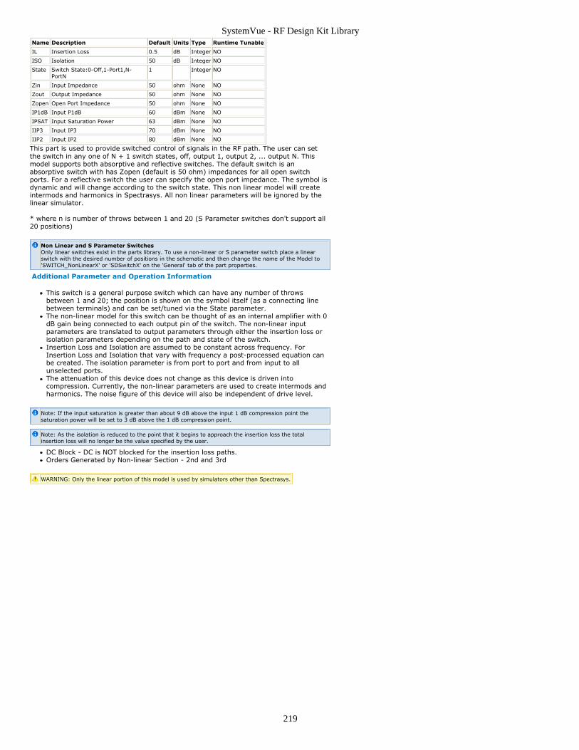
SystemVue - RF Design Kit Library
219
Name Description Default Units Type Runtime Tunable
IL Insertion Loss 0.5 dB Integer NO
ISO Isolation 50 dB Integer NO
State Switch State:0-Off,1-Port1,N-PortN
1 Integer NO
Zin Input Impedance 50 ohm None NO
Zout Output Impedance 50 ohm None NO
Zopen Open Port Impedance 50 ohm None NO
IP1dB Input P1dB 60 dBm None NO
IPSAT Input Saturation Power 63 dBm None NO
IIP3 Input IP3 70 dBm None NO
IIP2 Input IP2 80 dBm None NO
This part is used to provide switched control of signals in the RF path. The user can setthe switch in any one of N + 1 switch states, off, output 1, output 2, ... output N. Thismodel supports both absorptive and reflective switches. The default switch is anabsorptive switch with has Zopen (default is 50 ohm) impedances for all open switchports. For a reflective switch the user can specify the open port impedance. The symbol isdynamic and will change according to the switch state. This non linear model will createintermods and harmonics in Spectrasys. All non linear parameters will be ignored by thelinear simulator.
* where n is number of throws between 1 and 20 (S Parameter switches don't support all20 positions)
Non Linear and S Parameter SwitchesOnly linear switches exist in the parts library. To use a non-linear or S parameter switch place a linearswitch with the desired number of positions in the schematic and then change the name of the Model to'SWITCH_NonLinearX' or 'SDSwitchX' on the 'General' tab of the part properties.
Additional Parameter and Operation Information
This switch is a general purpose switch which can have any number of throwsbetween 1 and 20; the position is shown on the symbol itself (as a connecting linebetween terminals) and can be set/tuned via the State parameter.The non-linear model for this switch can be thought of as an internal amplifier with 0dB gain being connected to each output pin of the switch. The non-linear inputparameters are translated to output parameters through either the insertion loss orisolation parameters depending on the path and state of the switch.Insertion Loss and Isolation are assumed to be constant across frequency. ForInsertion Loss and Isolation that vary with frequency a post-processed equation canbe created. The isolation parameter is from port to port and from input to allunselected ports.The attenuation of this device does not change as this device is driven intocompression. Currently, the non-linear parameters are used to create intermods andharmonics. The noise figure of this device will also be independent of drive level.
Note: If the input saturation is greater than about 9 dB above the input 1 dB compression point thesaturation power will be set to 3 dB above the 1 dB compression point.
Note: As the isolation is reduced to the point that it begins to approach the insertion loss the totalinsertion loss will no longer be the value specified by the user.
DC Block - DC is NOT blocked for the insertion loss paths.Orders Generated by Non-linear Section - 2nd and 3rd
WARNING: Only the linear portion of this model is used by simulators other than Spectrasys.

SystemVue - RF Design Kit Library
220
Switch(SP15T) Part Switch - SP15T
Categories: System (rfdesign)
The models associated with this part are listed below. To view detailed information on amodel (description, parameters, equations, notes, etc.), please click the appropriate link.
Model
SWITCH_Linear15 (rfdesign)
SWITCH_NonLinear15 (rfdesign)
SWITCH_Linear15
Description: Switch - SP15TAssociated Parts: Switch(SP15T) Part (rfdesign)
Model Parameters
Name Description Default Units Type Runtime Tunable
IL Insertion Loss 0.5 dB Integer NO
ISO Isolation 50 dB Integer NO
State Switch State:0-Off,1-Port1,N-PortN
1 Integer NO
Zin Input Impedance 50 ohm None NO
Zout Output Impedance 50 ohm None NO
Zopen Open Port Impedance 50 ohm None NO
This part is used to provide switched control of signals in the RF path. The user can setthe switch in any one of N + 1 switch states, off, output 1, output 2, ... output N. Thismodel supports both absorptive and reflective switches. The default switch is anabsorptive switch with has Zopen (default is 50 ohm) impedances for all open switchports. For a reflective switch the user can specify the open port impedance. The symbol isdynamic and will change according to the switch state. The linear switch part alsosupports a non-linear and S parameter based models.
* where n is number of throws between 1 and 20 (S Parameter switches don't support all20 positions)
Non Linear and S Parameter SwitchesOnly linear switches exist in the parts library. To use a non-linear or S parameter switch place a linearswitch with the desired number of positions in the schematic and then change the name of the Model to'SWITCH_NonLinearX' or 'SDSwitchX' on the 'General' tab of the part properties.
Additional Parameter/Operation Information
This switch is a general purpose switch which can have any number of throws between 1and 20; the position is shown on the symbol itself (as a connecting line betweenterminals) and can be set/tuned via the State parameter.
The non-linear model for this switch can be thought of as an internal amplifier with 0 dBgain being connected to each output pin of the switch. The non-linear input parametersare translated to output parameters through either the insertion loss or isolationparameters depending on the path and state of the switch.
Insertion Loss and Isolation are assumed to be constant across frequency. For InsertionLoss and Isolation that vary with frequency a post-processed equation can be created withthe FREQ variable. The isolation parameter is from port to port and from input to allunselected ports.
The attenuation of this device does not change as this device is driven into compression.Currently, the non-linear parameters are used to create intermods and harmonics. Thenoise figure of this device will also be independent of drive level.
Note: As the isolation is reduced to the point that it begins to approach the insertion loss the totalinsertion loss will no longer be the value specified by the user.
DC Block - DC is NOT blocked for the insertion loss paths.
WARNING: Only the linear portion of this model is used by simulators other than Spectrasys.
SWITCH_NonLinear15
Description: Switch - SP15TAssociated Parts: Switch(SP15T) Part (rfdesign)
Model Parameters

SystemVue - RF Design Kit Library
221
Name Description Default Units Type Runtime Tunable
IL Insertion Loss 0.5 dB Integer NO
ISO Isolation 50 dB Integer NO
State Switch State:0-Off,1-Port1,N-PortN
1 Integer NO
Zin Input Impedance 50 ohm None NO
Zout Output Impedance 50 ohm None NO
Zopen Open Port Impedance 50 ohm None NO
IP1dB Input P1dB 60 dBm None NO
IPSAT Input Saturation Power 63 dBm None NO
IIP3 Input IP3 70 dBm None NO
IIP2 Input IP2 80 dBm None NO
This part is used to provide switched control of signals in the RF path. The user can setthe switch in any one of N + 1 switch states, off, output 1, output 2, ... output N. Thismodel supports both absorptive and reflective switches. The default switch is anabsorptive switch with has Zopen (default is 50 ohm) impedances for all open switchports. For a reflective switch the user can specify the open port impedance. The symbol isdynamic and will change according to the switch state. This non linear model will createintermods and harmonics in Spectrasys. All non linear parameters will be ignored by thelinear simulator.
* where n is number of throws between 1 and 20 (S Parameter switches don't support all20 positions)
Non Linear and S Parameter SwitchesOnly linear switches exist in the parts library. To use a non-linear or S parameter switch place a linearswitch with the desired number of positions in the schematic and then change the name of the Model to'SWITCH_NonLinearX' or 'SDSwitchX' on the 'General' tab of the part properties.
Additional Parameter and Operation Information
This switch is a general purpose switch which can have any number of throwsbetween 1 and 20; the position is shown on the symbol itself (as a connecting linebetween terminals) and can be set/tuned via the State parameter.The non-linear model for this switch can be thought of as an internal amplifier with 0dB gain being connected to each output pin of the switch. The non-linear inputparameters are translated to output parameters through either the insertion loss orisolation parameters depending on the path and state of the switch.Insertion Loss and Isolation are assumed to be constant across frequency. ForInsertion Loss and Isolation that vary with frequency a post-processed equation canbe created. The isolation parameter is from port to port and from input to allunselected ports.The attenuation of this device does not change as this device is driven intocompression. Currently, the non-linear parameters are used to create intermods andharmonics. The noise figure of this device will also be independent of drive level.
Note: If the input saturation is greater than about 9 dB above the input 1 dB compression point thesaturation power will be set to 3 dB above the 1 dB compression point.
Note: As the isolation is reduced to the point that it begins to approach the insertion loss the totalinsertion loss will no longer be the value specified by the user.
DC Block - DC is NOT blocked for the insertion loss paths.Orders Generated by Non-linear Section - 2nd and 3rd
WARNING: Only the linear portion of this model is used by simulators other than Spectrasys.

SystemVue - RF Design Kit Library
222
Switch(SP16T) Part Switch - SP16T
Categories: System (rfdesign)
The models associated with this part are listed below. To view detailed information on amodel (description, parameters, equations, notes, etc.), please click the appropriate link.
Model
SWITCH_Linear16 (rfdesign)
SWITCH_NonLinear16 (rfdesign)
SWITCH_Linear16
Description: Switch - SP16TAssociated Parts: Switch(SP16T) Part (rfdesign)
Model Parameters
Name Description Default Units Type Runtime Tunable
IL Insertion Loss 0.5 dB Integer NO
ISO Isolation 50 dB Integer NO
State Switch State:0-Off,1-Port1,N-PortN
1 Integer NO
Zin Input Impedance 50 ohm None NO
Zout Output Impedance 50 ohm None NO
Zopen Open Port Impedance 50 ohm None NO
This part is used to provide switched control of signals in the RF path. The user can setthe switch in any one of N + 1 switch states, off, output 1, output 2, ... output N. Thismodel supports both absorptive and reflective switches. The default switch is anabsorptive switch with has Zopen (default is 50 ohm) impedances for all open switchports. For a reflective switch the user can specify the open port impedance. The symbol isdynamic and will change according to the switch state. The linear switch part alsosupports a non-linear and S parameter based models.
* where n is number of throws between 1 and 20 (S Parameter switches don't support all20 positions)
Non Linear and S Parameter SwitchesOnly linear switches exist in the parts library. To use a non-linear or S parameter switch place a linearswitch with the desired number of positions in the schematic and then change the name of the Model to'SWITCH_NonLinearX' or 'SDSwitchX' on the 'General' tab of the part properties.
Additional Parameter/Operation Information
This switch is a general purpose switch which can have any number of throws between 1and 20; the position is shown on the symbol itself (as a connecting line betweenterminals) and can be set/tuned via the State parameter.
The non-linear model for this switch can be thought of as an internal amplifier with 0 dBgain being connected to each output pin of the switch. The non-linear input parametersare translated to output parameters through either the insertion loss or isolationparameters depending on the path and state of the switch.
Insertion Loss and Isolation are assumed to be constant across frequency. For InsertionLoss and Isolation that vary with frequency a post-processed equation can be created withthe FREQ variable. The isolation parameter is from port to port and from input to allunselected ports.
The attenuation of this device does not change as this device is driven into compression.Currently, the non-linear parameters are used to create intermods and harmonics. Thenoise figure of this device will also be independent of drive level.
Note: As the isolation is reduced to the point that it begins to approach the insertion loss the totalinsertion loss will no longer be the value specified by the user.
DC Block - DC is NOT blocked for the insertion loss paths.
WARNING: Only the linear portion of this model is used by simulators other than Spectrasys.
SWITCH_NonLinear16
Description: Switch - SP16TAssociated Parts: Switch(SP16T) Part (rfdesign)
Model Parameters

SystemVue - RF Design Kit Library
223
Name Description Default Units Type Runtime Tunable
IL Insertion Loss 0.5 dB Integer NO
ISO Isolation 50 dB Integer NO
State Switch State:0-Off,1-Port1,N-PortN
1 Integer NO
Zin Input Impedance 50 ohm None NO
Zout Output Impedance 50 ohm None NO
Zopen Open Port Impedance 50 ohm None NO
IP1dB Input P1dB 60 dBm None NO
IPSAT Input Saturation Power 63 dBm None NO
IIP3 Input IP3 70 dBm None NO
IIP2 Input IP2 80 dBm None NO
This part is used to provide switched control of signals in the RF path. The user can setthe switch in any one of N + 1 switch states, off, output 1, output 2, ... output N. Thismodel supports both absorptive and reflective switches. The default switch is anabsorptive switch with has Zopen (default is 50 ohm) impedances for all open switchports. For a reflective switch the user can specify the open port impedance. The symbol isdynamic and will change according to the switch state. This non linear model will createintermods and harmonics in Spectrasys. All non linear parameters will be ignored by thelinear simulator.
* where n is number of throws between 1 and 20 (S Parameter switches don't support all20 positions)
Non Linear and S Parameter SwitchesOnly linear switches exist in the parts library. To use a non-linear or S parameter switch place a linearswitch with the desired number of positions in the schematic and then change the name of the Model to'SWITCH_NonLinearX' or 'SDSwitchX' on the 'General' tab of the part properties.
Additional Parameter and Operation Information
This switch is a general purpose switch which can have any number of throwsbetween 1 and 20; the position is shown on the symbol itself (as a connecting linebetween terminals) and can be set/tuned via the State parameter.The non-linear model for this switch can be thought of as an internal amplifier with 0dB gain being connected to each output pin of the switch. The non-linear inputparameters are translated to output parameters through either the insertion loss orisolation parameters depending on the path and state of the switch.Insertion Loss and Isolation are assumed to be constant across frequency. ForInsertion Loss and Isolation that vary with frequency a post-processed equation canbe created. The isolation parameter is from port to port and from input to allunselected ports.The attenuation of this device does not change as this device is driven intocompression. Currently, the non-linear parameters are used to create intermods andharmonics. The noise figure of this device will also be independent of drive level.
Note: If the input saturation is greater than about 9 dB above the input 1 dB compression point thesaturation power will be set to 3 dB above the 1 dB compression point.
Note: As the isolation is reduced to the point that it begins to approach the insertion loss the totalinsertion loss will no longer be the value specified by the user.
DC Block - DC is NOT blocked for the insertion loss paths.Orders Generated by Non-linear Section - 2nd and 3rd
WARNING: Only the linear portion of this model is used by simulators other than Spectrasys.

SystemVue - RF Design Kit Library
224
Switch(SP17T) Part Switch - SP17T
Categories: System (rfdesign)
The models associated with this part are listed below. To view detailed information on amodel (description, parameters, equations, notes, etc.), please click the appropriate link.
Model
SWITCH_Linear17 (rfdesign)
SWITCH_NonLinear17 (rfdesign)
SWITCH_Linear17
Description: Switch - SP17TAssociated Parts: Switch(SP17T) Part (rfdesign)
Model Parameters
Name Description Default Units Type Runtime Tunable
IL Insertion Loss 0.5 dB Integer NO
ISO Isolation 50 dB Integer NO
State Switch State:0-Off,1-Port1,N-PortN
1 Integer NO
Zin Input Impedance 50 ohm None NO
Zout Output Impedance 50 ohm None NO
Zopen Open Port Impedance 50 ohm None NO
This part is used to provide switched control of signals in the RF path. The user can setthe switch in any one of N + 1 switch states, off, output 1, output 2, ... output N. Thismodel supports both absorptive and reflective switches. The default switch is anabsorptive switch with has Zopen (default is 50 ohm) impedances for all open switchports. For a reflective switch the user can specify the open port impedance. The symbol isdynamic and will change according to the switch state. The linear switch part alsosupports a non-linear and S parameter based models.
* where n is number of throws between 1 and 20 (S Parameter switches don't support all20 positions)
Non Linear and S Parameter SwitchesOnly linear switches exist in the parts library. To use a non-linear or S parameter switch place a linearswitch with the desired number of positions in the schematic and then change the name of the Model to'SWITCH_NonLinearX' or 'SDSwitchX' on the 'General' tab of the part properties.
Additional Parameter/Operation Information
This switch is a general purpose switch which can have any number of throws between 1and 20; the position is shown on the symbol itself (as a connecting line betweenterminals) and can be set/tuned via the State parameter.
The non-linear model for this switch can be thought of as an internal amplifier with 0 dBgain being connected to each output pin of the switch. The non-linear input parametersare translated to output parameters through either the insertion loss or isolationparameters depending on the path and state of the switch.
Insertion Loss and Isolation are assumed to be constant across frequency. For InsertionLoss and Isolation that vary with frequency a post-processed equation can be created withthe FREQ variable. The isolation parameter is from port to port and from input to allunselected ports.
The attenuation of this device does not change as this device is driven into compression.Currently, the non-linear parameters are used to create intermods and harmonics. Thenoise figure of this device will also be independent of drive level.
Note: As the isolation is reduced to the point that it begins to approach the insertion loss the totalinsertion loss will no longer be the value specified by the user.
DC Block - DC is NOT blocked for the insertion loss paths.
WARNING: Only the linear portion of this model is used by simulators other than Spectrasys.
SWITCH_NonLinear17
Description: Switch - SP17TAssociated Parts: Switch(SP17T) Part (rfdesign)
Model Parameters

SystemVue - RF Design Kit Library
225
Name Description Default Units Type Runtime Tunable
IL Insertion Loss 0.5 dB Integer NO
ISO Isolation 50 dB Integer NO
State Switch State:0-Off,1-Port1,N-PortN
1 Integer NO
Zin Input Impedance 50 ohm None NO
Zout Output Impedance 50 ohm None NO
Zopen Open Port Impedance 50 ohm None NO
IP1dB Input P1dB 60 dBm None NO
IPSAT Input Saturation Power 63 dBm None NO
IIP3 Input IP3 70 dBm None NO
IIP2 Input IP2 80 dBm None NO
This part is used to provide switched control of signals in the RF path. The user can setthe switch in any one of N + 1 switch states, off, output 1, output 2, ... output N. Thismodel supports both absorptive and reflective switches. The default switch is anabsorptive switch with has Zopen (default is 50 ohm) impedances for all open switchports. For a reflective switch the user can specify the open port impedance. The symbol isdynamic and will change according to the switch state. This non linear model will createintermods and harmonics in Spectrasys. All non linear parameters will be ignored by thelinear simulator.
* where n is number of throws between 1 and 20 (S Parameter switches don't support all20 positions)
Non Linear and S Parameter SwitchesOnly linear switches exist in the parts library. To use a non-linear or S parameter switch place a linearswitch with the desired number of positions in the schematic and then change the name of the Model to'SWITCH_NonLinearX' or 'SDSwitchX' on the 'General' tab of the part properties.
Additional Parameter and Operation Information
This switch is a general purpose switch which can have any number of throwsbetween 1 and 20; the position is shown on the symbol itself (as a connecting linebetween terminals) and can be set/tuned via the State parameter.The non-linear model for this switch can be thought of as an internal amplifier with 0dB gain being connected to each output pin of the switch. The non-linear inputparameters are translated to output parameters through either the insertion loss orisolation parameters depending on the path and state of the switch.Insertion Loss and Isolation are assumed to be constant across frequency. ForInsertion Loss and Isolation that vary with frequency a post-processed equation canbe created. The isolation parameter is from port to port and from input to allunselected ports.The attenuation of this device does not change as this device is driven intocompression. Currently, the non-linear parameters are used to create intermods andharmonics. The noise figure of this device will also be independent of drive level.
Note: If the input saturation is greater than about 9 dB above the input 1 dB compression point thesaturation power will be set to 3 dB above the 1 dB compression point.
Note: As the isolation is reduced to the point that it begins to approach the insertion loss the totalinsertion loss will no longer be the value specified by the user.
DC Block - DC is NOT blocked for the insertion loss paths.Orders Generated by Non-linear Section - 2nd and 3rd
WARNING: Only the linear portion of this model is used by simulators other than Spectrasys.

SystemVue - RF Design Kit Library
226
Switch(SP18T) Part Switch - SP18T
Categories: System (rfdesign)
The models associated with this part are listed below. To view detailed information on amodel (description, parameters, equations, notes, etc.), please click the appropriate link.
Model
SWITCH_Linear18 (rfdesign)
SWITCH_NonLinear18 (rfdesign)
SWITCH_Linear18
Description: Switch - SP18TAssociated Parts: Switch(SP18T) Part (rfdesign)
Model Parameters
Name Description Default Units Type Runtime Tunable
IL Insertion Loss 0.5 dB Integer NO
ISO Isolation 50 dB Integer NO
State Switch State:0-Off,1-Port1,N-PortN
1 Integer NO
Zin Input Impedance 50 ohm None NO
Zout Output Impedance 50 ohm None NO
Zopen Open Port Impedance 50 ohm None NO
This part is used to provide switched control of signals in the RF path. The user can setthe switch in any one of N + 1 switch states, off, output 1, output 2, ... output N. Thismodel supports both absorptive and reflective switches. The default switch is anabsorptive switch with has Zopen (default is 50 ohm) impedances for all open switchports. For a reflective switch the user can specify the open port impedance. The symbol isdynamic and will change according to the switch state. The linear switch part alsosupports a non-linear and S parameter based models.
* where n is number of throws between 1 and 20 (S Parameter switches don't support all20 positions)
Non Linear and S Parameter SwitchesOnly linear switches exist in the parts library. To use a non-linear or S parameter switch place a linearswitch with the desired number of positions in the schematic and then change the name of the Model to'SWITCH_NonLinearX' or 'SDSwitchX' on the 'General' tab of the part properties.
Additional Parameter/Operation Information
This switch is a general purpose switch which can have any number of throws between 1and 20; the position is shown on the symbol itself (as a connecting line betweenterminals) and can be set/tuned via the State parameter.
The non-linear model for this switch can be thought of as an internal amplifier with 0 dBgain being connected to each output pin of the switch. The non-linear input parametersare translated to output parameters through either the insertion loss or isolationparameters depending on the path and state of the switch.
Insertion Loss and Isolation are assumed to be constant across frequency. For InsertionLoss and Isolation that vary with frequency a post-processed equation can be created withthe FREQ variable. The isolation parameter is from port to port and from input to allunselected ports.
The attenuation of this device does not change as this device is driven into compression.Currently, the non-linear parameters are used to create intermods and harmonics. Thenoise figure of this device will also be independent of drive level.
Note: As the isolation is reduced to the point that it begins to approach the insertion loss the totalinsertion loss will no longer be the value specified by the user.
DC Block - DC is NOT blocked for the insertion loss paths.
WARNING: Only the linear portion of this model is used by simulators other than Spectrasys.
SWITCH_NonLinear18
Description: Switch - SP18TAssociated Parts: Switch(SP18T) Part (rfdesign)
Model Parameters

SystemVue - RF Design Kit Library
227
Name Description Default Units Type Runtime Tunable
IL Insertion Loss 0.5 dB Integer NO
ISO Isolation 50 dB Integer NO
State Switch State:0-Off,1-Port1,N-PortN
1 Integer NO
Zin Input Impedance 50 ohm None NO
Zout Output Impedance 50 ohm None NO
Zopen Open Port Impedance 50 ohm None NO
IP1dB Input P1dB 60 dBm None NO
IPSAT Input Saturation Power 63 dBm None NO
IIP3 Input IP3 70 dBm None NO
IIP2 Input IP2 80 dBm None NO
This part is used to provide switched control of signals in the RF path. The user can setthe switch in any one of N + 1 switch states, off, output 1, output 2, ... output N. Thismodel supports both absorptive and reflective switches. The default switch is anabsorptive switch with has Zopen (default is 50 ohm) impedances for all open switchports. For a reflective switch the user can specify the open port impedance. The symbol isdynamic and will change according to the switch state. This non linear model will createintermods and harmonics in Spectrasys. All non linear parameters will be ignored by thelinear simulator.
* where n is number of throws between 1 and 20 (S Parameter switches don't support all20 positions)
Non Linear and S Parameter SwitchesOnly linear switches exist in the parts library. To use a non-linear or S parameter switch place a linearswitch with the desired number of positions in the schematic and then change the name of the Model to'SWITCH_NonLinearX' or 'SDSwitchX' on the 'General' tab of the part properties.
Additional Parameter and Operation Information
This switch is a general purpose switch which can have any number of throwsbetween 1 and 20; the position is shown on the symbol itself (as a connecting linebetween terminals) and can be set/tuned via the State parameter.The non-linear model for this switch can be thought of as an internal amplifier with 0dB gain being connected to each output pin of the switch. The non-linear inputparameters are translated to output parameters through either the insertion loss orisolation parameters depending on the path and state of the switch.Insertion Loss and Isolation are assumed to be constant across frequency. ForInsertion Loss and Isolation that vary with frequency a post-processed equation canbe created. The isolation parameter is from port to port and from input to allunselected ports.The attenuation of this device does not change as this device is driven intocompression. Currently, the non-linear parameters are used to create intermods andharmonics. The noise figure of this device will also be independent of drive level.
Note: If the input saturation is greater than about 9 dB above the input 1 dB compression point thesaturation power will be set to 3 dB above the 1 dB compression point.
Note: As the isolation is reduced to the point that it begins to approach the insertion loss the totalinsertion loss will no longer be the value specified by the user.
DC Block - DC is NOT blocked for the insertion loss paths.Orders Generated by Non-linear Section - 2nd and 3rd
WARNING: Only the linear portion of this model is used by simulators other than Spectrasys.
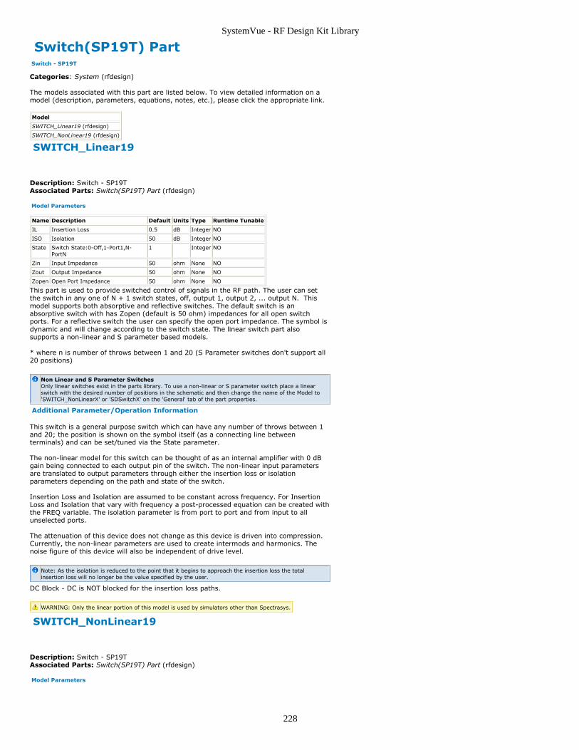
SystemVue - RF Design Kit Library
228
Switch(SP19T) Part Switch - SP19T
Categories: System (rfdesign)
The models associated with this part are listed below. To view detailed information on amodel (description, parameters, equations, notes, etc.), please click the appropriate link.
Model
SWITCH_Linear19 (rfdesign)
SWITCH_NonLinear19 (rfdesign)
SWITCH_Linear19
Description: Switch - SP19TAssociated Parts: Switch(SP19T) Part (rfdesign)
Model Parameters
Name Description Default Units Type Runtime Tunable
IL Insertion Loss 0.5 dB Integer NO
ISO Isolation 50 dB Integer NO
State Switch State:0-Off,1-Port1,N-PortN
1 Integer NO
Zin Input Impedance 50 ohm None NO
Zout Output Impedance 50 ohm None NO
Zopen Open Port Impedance 50 ohm None NO
This part is used to provide switched control of signals in the RF path. The user can setthe switch in any one of N + 1 switch states, off, output 1, output 2, ... output N. Thismodel supports both absorptive and reflective switches. The default switch is anabsorptive switch with has Zopen (default is 50 ohm) impedances for all open switchports. For a reflective switch the user can specify the open port impedance. The symbol isdynamic and will change according to the switch state. The linear switch part alsosupports a non-linear and S parameter based models.
* where n is number of throws between 1 and 20 (S Parameter switches don't support all20 positions)
Non Linear and S Parameter SwitchesOnly linear switches exist in the parts library. To use a non-linear or S parameter switch place a linearswitch with the desired number of positions in the schematic and then change the name of the Model to'SWITCH_NonLinearX' or 'SDSwitchX' on the 'General' tab of the part properties.
Additional Parameter/Operation Information
This switch is a general purpose switch which can have any number of throws between 1and 20; the position is shown on the symbol itself (as a connecting line betweenterminals) and can be set/tuned via the State parameter.
The non-linear model for this switch can be thought of as an internal amplifier with 0 dBgain being connected to each output pin of the switch. The non-linear input parametersare translated to output parameters through either the insertion loss or isolationparameters depending on the path and state of the switch.
Insertion Loss and Isolation are assumed to be constant across frequency. For InsertionLoss and Isolation that vary with frequency a post-processed equation can be created withthe FREQ variable. The isolation parameter is from port to port and from input to allunselected ports.
The attenuation of this device does not change as this device is driven into compression.Currently, the non-linear parameters are used to create intermods and harmonics. Thenoise figure of this device will also be independent of drive level.
Note: As the isolation is reduced to the point that it begins to approach the insertion loss the totalinsertion loss will no longer be the value specified by the user.
DC Block - DC is NOT blocked for the insertion loss paths.
WARNING: Only the linear portion of this model is used by simulators other than Spectrasys.
SWITCH_NonLinear19
Description: Switch - SP19TAssociated Parts: Switch(SP19T) Part (rfdesign)
Model Parameters

SystemVue - RF Design Kit Library
229
Name Description Default Units Type Runtime Tunable
IL Insertion Loss 0.5 dB Integer NO
ISO Isolation 50 dB Integer NO
State Switch State:0-Off,1-Port1,N-PortN
1 Integer NO
Zin Input Impedance 50 ohm None NO
Zout Output Impedance 50 ohm None NO
Zopen Open Port Impedance 50 ohm None NO
IP1dB Input P1dB 60 dBm None NO
IPSAT Input Saturation Power 63 dBm None NO
IIP3 Input IP3 70 dBm None NO
IIP2 Input IP2 80 dBm None NO
This part is used to provide switched control of signals in the RF path. The user can setthe switch in any one of N + 1 switch states, off, output 1, output 2, ... output N. Thismodel supports both absorptive and reflective switches. The default switch is anabsorptive switch with has Zopen (default is 50 ohm) impedances for all open switchports. For a reflective switch the user can specify the open port impedance. The symbol isdynamic and will change according to the switch state. This non linear model will createintermods and harmonics in Spectrasys. All non linear parameters will be ignored by thelinear simulator.
* where n is number of throws between 1 and 20 (S Parameter switches don't support all20 positions)
Non Linear and S Parameter SwitchesOnly linear switches exist in the parts library. To use a non-linear or S parameter switch place a linearswitch with the desired number of positions in the schematic and then change the name of the Model to'SWITCH_NonLinearX' or 'SDSwitchX' on the 'General' tab of the part properties.
Additional Parameter and Operation Information
This switch is a general purpose switch which can have any number of throwsbetween 1 and 20; the position is shown on the symbol itself (as a connecting linebetween terminals) and can be set/tuned via the State parameter.The non-linear model for this switch can be thought of as an internal amplifier with 0dB gain being connected to each output pin of the switch. The non-linear inputparameters are translated to output parameters through either the insertion loss orisolation parameters depending on the path and state of the switch.Insertion Loss and Isolation are assumed to be constant across frequency. ForInsertion Loss and Isolation that vary with frequency a post-processed equation canbe created. The isolation parameter is from port to port and from input to allunselected ports.The attenuation of this device does not change as this device is driven intocompression. Currently, the non-linear parameters are used to create intermods andharmonics. The noise figure of this device will also be independent of drive level.
Note: If the input saturation is greater than about 9 dB above the input 1 dB compression point thesaturation power will be set to 3 dB above the 1 dB compression point.
Note: As the isolation is reduced to the point that it begins to approach the insertion loss the totalinsertion loss will no longer be the value specified by the user.
DC Block - DC is NOT blocked for the insertion loss paths.Orders Generated by Non-linear Section - 2nd and 3rd
WARNING: Only the linear portion of this model is used by simulators other than Spectrasys.

SystemVue - RF Design Kit Library
230
Switch(SP20T) Part Switch - SP20T
Categories: System (rfdesign)
The models associated with this part are listed below. To view detailed information on amodel (description, parameters, equations, notes, etc.), please click the appropriate link.
Model
SWITCH_Linear20 (rfdesign)
SWITCH_NonLinear20 (rfdesign)
SWITCH_Linear20
Description: Switch - SP20TAssociated Parts: Switch(SP20T) Part (rfdesign)
Model Parameters
Name Description Default Units Type Runtime Tunable
IL Insertion Loss 0.5 dB Integer NO
ISO Isolation 50 dB Integer NO
State Switch State:0-Off,1-Port1,N-PortN
1 Integer NO
Zin Input Impedance 50 ohm None NO
Zout Output Impedance 50 ohm None NO
Zopen Open Port Impedance 50 ohm None NO
This part is used to provide switched control of signals in the RF path. The user can setthe switch in any one of N + 1 switch states, off, output 1, output 2, ... output N. Thismodel supports both absorptive and reflective switches. The default switch is anabsorptive switch with has Zopen (default is 50 ohm) impedances for all open switchports. For a reflective switch the user can specify the open port impedance. The symbol isdynamic and will change according to the switch state. The linear switch part alsosupports a non-linear and S parameter based models.
* where n is number of throws between 1 and 20 (S Parameter switches don't support all20 positions)
Non Linear and S Parameter SwitchesOnly linear switches exist in the parts library. To use a non-linear or S parameter switch place a linearswitch with the desired number of positions in the schematic and then change the name of the Model to'SWITCH_NonLinearX' or 'SDSwitchX' on the 'General' tab of the part properties.
Additional Parameter/Operation Information
This switch is a general purpose switch which can have any number of throws between 1and 20; the position is shown on the symbol itself (as a connecting line betweenterminals) and can be set/tuned via the State parameter.
The non-linear model for this switch can be thought of as an internal amplifier with 0 dBgain being connected to each output pin of the switch. The non-linear input parametersare translated to output parameters through either the insertion loss or isolationparameters depending on the path and state of the switch.
Insertion Loss and Isolation are assumed to be constant across frequency. For InsertionLoss and Isolation that vary with frequency a post-processed equation can be created withthe FREQ variable. The isolation parameter is from port to port and from input to allunselected ports.
The attenuation of this device does not change as this device is driven into compression.Currently, the non-linear parameters are used to create intermods and harmonics. Thenoise figure of this device will also be independent of drive level.
Note: As the isolation is reduced to the point that it begins to approach the insertion loss the totalinsertion loss will no longer be the value specified by the user.
DC Block - DC is NOT blocked for the insertion loss paths.
WARNING: Only the linear portion of this model is used by simulators other than Spectrasys.
SWITCH_NonLinear20
Description: Switch - SP20TAssociated Parts: Switch(SP20T) Part (rfdesign)
Model Parameters

SystemVue - RF Design Kit Library
231
Name Description Default Units Type Runtime Tunable
IL Insertion Loss 0.5 dB Integer NO
ISO Isolation 50 dB Integer NO
State Switch State:0-Off,1-Port1,N-PortN
1 Integer NO
Zin Input Impedance 50 ohm None NO
Zout Output Impedance 50 ohm None NO
Zopen Open Port Impedance 50 ohm None NO
IP1dB Input P1dB 60 dBm None NO
IPSAT Input Saturation Power 63 dBm None NO
IIP3 Input IP3 70 dBm None NO
IIP2 Input IP2 80 dBm None NO
This part is used to provide switched control of signals in the RF path. The user can setthe switch in any one of N + 1 switch states, off, output 1, output 2, ... output N. Thismodel supports both absorptive and reflective switches. The default switch is anabsorptive switch with has Zopen (default is 50 ohm) impedances for all open switchports. For a reflective switch the user can specify the open port impedance. The symbol isdynamic and will change according to the switch state. This non linear model will createintermods and harmonics in Spectrasys. All non linear parameters will be ignored by thelinear simulator.
* where n is number of throws between 1 and 20 (S Parameter switches don't support all20 positions)
Non Linear and S Parameter SwitchesOnly linear switches exist in the parts library. To use a non-linear or S parameter switch place a linearswitch with the desired number of positions in the schematic and then change the name of the Model to'SWITCH_NonLinearX' or 'SDSwitchX' on the 'General' tab of the part properties.
Additional Parameter and Operation Information
This switch is a general purpose switch which can have any number of throwsbetween 1 and 20; the position is shown on the symbol itself (as a connecting linebetween terminals) and can be set/tuned via the State parameter.The non-linear model for this switch can be thought of as an internal amplifier with 0dB gain being connected to each output pin of the switch. The non-linear inputparameters are translated to output parameters through either the insertion loss orisolation parameters depending on the path and state of the switch.Insertion Loss and Isolation are assumed to be constant across frequency. ForInsertion Loss and Isolation that vary with frequency a post-processed equation canbe created. The isolation parameter is from port to port and from input to allunselected ports.The attenuation of this device does not change as this device is driven intocompression. Currently, the non-linear parameters are used to create intermods andharmonics. The noise figure of this device will also be independent of drive level.
Note: If the input saturation is greater than about 9 dB above the input 1 dB compression point thesaturation power will be set to 3 dB above the 1 dB compression point.
Note: As the isolation is reduced to the point that it begins to approach the insertion loss the totalinsertion loss will no longer be the value specified by the user.
DC Block - DC is NOT blocked for the insertion loss paths.Orders Generated by Non-linear Section - 2nd and 3rd
WARNING: Only the linear portion of this model is used by simulators other than Spectrasys.

SystemVue - RF Design Kit Library
232
Switch(SPDT) Part Switch - SPDT
Categories: System (rfdesign)
The models associated with this part are listed below. To view detailed information on amodel (description, parameters, equations, notes, etc.), please click the appropriate link.
Model
SWITCH_Linear2 (rfdesign)
SWITCH_NonLinear2 (rfdesign)
SDSwitch2 (rfdesign)
SDSwitch2
Description: Switch - SPDTAssociated Parts: Switch(SPDT) Part (rfdesign)
Model Parameters
Name Description Default Units Type Runtime Tunable
State Switch State 0-Off, 1-Port1,N-PortN 1 Integer NO
SData1 State 1 S Parameters Text NO
SData2 State 2 S Parameters Text NO
IP1DB Input 1 dB Compression Point 60 dBm Float NO
IPSAT Input Saturation Point 63 dBm Float NO
IIP3 Input 3rd Order Intercept Point 70 dBm Float NO
IIP2 Input 2nd Order Intercept Point 80 dBm Float NO
Zo Reference Impedance 50 ohm Float NO
SDataOff Off State S Parameters Text NO
This part is used to provide switched control of signals in the RF path. The user can setthe switch in any one of N + 1 switch states, off, output 1, output 2, ... output N. Thesymbol is dynamic and will change according to the switch state. S parameters arespecified for each of the switch states including the off state. The non linear characteristicsapply to every switch port. The non linearities are first applied to the input signalsfollowed by the S parameters. This model will create intermods and harmonics inSpectrasys. All non linear parameters will be ignored by the linear simulator.
* where n is number of throws (1, 2, 3, 4, 6, and 8)
Non Linear and S Parameter SwitchesOnly linear switches exist in the parts library. To use a non-linear or S parameter switch place a linearswitch with the desired number of positions in the schematic and then change the name of the Model to'SWITCH_NonLinearX' or 'SDSwitchX' on the 'General' tab of the part properties.
^ S Parameters are specified for each switch state, N is the switch state
Additional Parameter Information
SData1 ... N This is the file name of the S parameter data for the given switch state (1 through N)
SDataOff This is the file name of the S parameter data for the off state of the switch
Additional Operation Information
The loss of the switch will change as it is driven into compression. The noise figure of thisdevice will also be dependent of drive level because of the compression.
Note: If the input saturation is greater than about 9 dB above the input 1 dB compression point thesaturation power will be set to 3 dB above the 1 dB compression point.
DC Block - DC is NOT blocked for the insertion loss paths.Orders Generated by Non-linear Section - 2nd and 3rd
WARNING: Only the linear portion of this model is used by simulators other than Spectrasys.
SWITCH_Linear2
Description: Switch - SPDTAssociated Parts: Switch(SPDT) Part (rfdesign)
Model Parameters

SystemVue - RF Design Kit Library
233
Name Description Default Units Type Runtime Tunable
IL Insertion Loss 0.5 dB Integer NO
ISO Isolation 50 dB Integer NO
State Switch State:0-Off,1-Port1,N-PortN
1 Integer NO
Zin Input Impedance 50 ohm None NO
Zout Output Impedance 50 ohm None NO
Zopen Open Port Impedance 50 ohm None NO
This part is used to provide switched control of signals in the RF path. The user can setthe switch in any one of N + 1 switch states, off, output 1, output 2, ... output N. Thismodel supports both absorptive and reflective switches. The default switch is anabsorptive switch with has Zopen (default is 50 ohm) impedances for all open switchports. For a reflective switch the user can specify the open port impedance. The symbol isdynamic and will change according to the switch state. The linear switch part alsosupports a non-linear and S parameter based models.
* where n is number of throws between 1 and 20 (S Parameter switches don't support all20 positions)
Non Linear and S Parameter SwitchesOnly linear switches exist in the parts library. To use a non-linear or S parameter switch place a linearswitch with the desired number of positions in the schematic and then change the name of the Model to'SWITCH_NonLinearX' or 'SDSwitchX' on the 'General' tab of the part properties.
Additional Parameter/Operation Information
This switch is a general purpose switch which can have any number of throws between 1and 20; the position is shown on the symbol itself (as a connecting line betweenterminals) and can be set/tuned via the State parameter.
The non-linear model for this switch can be thought of as an internal amplifier with 0 dBgain being connected to each output pin of the switch. The non-linear input parametersare translated to output parameters through either the insertion loss or isolationparameters depending on the path and state of the switch.
Insertion Loss and Isolation are assumed to be constant across frequency. For InsertionLoss and Isolation that vary with frequency a post-processed equation can be created withthe FREQ variable. The isolation parameter is from port to port and from input to allunselected ports.
The attenuation of this device does not change as this device is driven into compression.Currently, the non-linear parameters are used to create intermods and harmonics. Thenoise figure of this device will also be independent of drive level.
Note: As the isolation is reduced to the point that it begins to approach the insertion loss the totalinsertion loss will no longer be the value specified by the user.
DC Block - DC is NOT blocked for the insertion loss paths.
WARNING: Only the linear portion of this model is used by simulators other than Spectrasys.
SWITCH_NonLinear2
Description: Switch - SPDTAssociated Parts: Switch(SPDT) Part (rfdesign)
Model Parameters
Name Description Default Units Type Runtime Tunable
IL Insertion Loss 0.5 dB Integer NO
ISO Isolation 50 dB Integer NO
State Switch State:0-Off,1-Port1,N-PortN
1 Integer NO
Zin Input Impedance 50 ohm None NO
Zout Output Impedance 50 ohm None NO
Zopen Open Port Impedance 50 ohm None NO
IP1dB Input P1dB 60 dBm None NO
IPSAT Input Saturation Power 63 dBm None NO
IIP3 Input IP3 70 dBm None NO
IIP2 Input IP2 80 dBm None NO
This part is used to provide switched control of signals in the RF path. The user can setthe switch in any one of N + 1 switch states, off, output 1, output 2, ... output N. Thismodel supports both absorptive and reflective switches. The default switch is anabsorptive switch with has Zopen (default is 50 ohm) impedances for all open switchports. For a reflective switch the user can specify the open port impedance. The symbol isdynamic and will change according to the switch state. This non linear model will createintermods and harmonics in Spectrasys. All non linear parameters will be ignored by thelinear simulator.
* where n is number of throws between 1 and 20 (S Parameter switches don't support all20 positions)

SystemVue - RF Design Kit Library
234
Non Linear and S Parameter SwitchesOnly linear switches exist in the parts library. To use a non-linear or S parameter switch place a linearswitch with the desired number of positions in the schematic and then change the name of the Model to'SWITCH_NonLinearX' or 'SDSwitchX' on the 'General' tab of the part properties.
Additional Parameter and Operation Information
This switch is a general purpose switch which can have any number of throwsbetween 1 and 20; the position is shown on the symbol itself (as a connecting linebetween terminals) and can be set/tuned via the State parameter.The non-linear model for this switch can be thought of as an internal amplifier with 0dB gain being connected to each output pin of the switch. The non-linear inputparameters are translated to output parameters through either the insertion loss orisolation parameters depending on the path and state of the switch.Insertion Loss and Isolation are assumed to be constant across frequency. ForInsertion Loss and Isolation that vary with frequency a post-processed equation canbe created. The isolation parameter is from port to port and from input to allunselected ports.The attenuation of this device does not change as this device is driven intocompression. Currently, the non-linear parameters are used to create intermods andharmonics. The noise figure of this device will also be independent of drive level.
Note: If the input saturation is greater than about 9 dB above the input 1 dB compression point thesaturation power will be set to 3 dB above the 1 dB compression point.
Note: As the isolation is reduced to the point that it begins to approach the insertion loss the totalinsertion loss will no longer be the value specified by the user.
DC Block - DC is NOT blocked for the insertion loss paths.Orders Generated by Non-linear Section - 2nd and 3rd
WARNING: Only the linear portion of this model is used by simulators other than Spectrasys.

SystemVue - RF Design Kit Library
235
Switch(SPST) Part Switch - SPST
Categories: System (rfdesign)
The models associated with this part are listed below. To view detailed information on amodel (description, parameters, equations, notes, etc.), please click the appropriate link.
Model
SWITCH_Linear1 (rfdesign)
SWITCH_NonLinear1 (rfdesign)
SDSwitch1 (rfdesign)
SDSwitch1
Description: Switch - SPSTAssociated Parts: Switch(SPST) Part (rfdesign)
Model Parameters
Name Description Default Units Type Runtime Tunable
State Switch State 0-Off, 1-On 1 Integer NO
SDataOn On State S Parameters Text NO
IP1DB Input 1 dB Compression Point 60 dBm Float NO
IPSAT Input Saturation Point 63 dBm Float NO
IIP3 Input 3rd Order Intercept Point 70 dBm Float NO
IIP2 Input 2nd Order Intercept Point 80 dBm Float NO
Zo Reference Impedance 50 ohm Float NO
SDataOff Off State S Parameters Text NO
This part is used to provide switched control of signals in the RF path. The user can setthe switch in any one of N + 1 switch states, off, output 1, output 2, ... output N. Thesymbol is dynamic and will change according to the switch state. S parameters arespecified for each of the switch states including the off state. The non linear characteristicsapply to every switch port. The non linearities are first applied to the input signalsfollowed by the S parameters. This model will create intermods and harmonics inSpectrasys. All non linear parameters will be ignored by the linear simulator.
* where n is number of throws (1, 2, 3, 4, 6, and 8)
Non Linear and S Parameter SwitchesOnly linear switches exist in the parts library. To use a non-linear or S parameter switch place a linearswitch with the desired number of positions in the schematic and then change the name of the Model to'SWITCH_NonLinearX' or 'SDSwitchX' on the 'General' tab of the part properties.
^ S Parameters are specified for each switch state, N is the switch state
Additional Parameter Information
SData1 ... N This is the file name of the S parameter data for the given switch state (1 through N)
SDataOff This is the file name of the S parameter data for the off state of the switch
Additional Operation Information
The loss of the switch will change as it is driven into compression. The noise figure of thisdevice will also be dependent of drive level because of the compression.
Note: If the input saturation is greater than about 9 dB above the input 1 dB compression point thesaturation power will be set to 3 dB above the 1 dB compression point.
DC Block - DC is NOT blocked for the insertion loss paths.Orders Generated by Non-linear Section - 2nd and 3rd
WARNING: Only the linear portion of this model is used by simulators other than Spectrasys.
SWITCH_Linear1
Description: Switch - SPSTAssociated Parts: Switch(SPST) Part (rfdesign)
Model Parameters

SystemVue - RF Design Kit Library
236
Name Description Default Units Type Runtime Tunable
IL Insertion Loss 0.5 dB Integer NO
ISO Isolation 50 dB Integer NO
State Switch State:0-Off,1-Port1,N-PortN
1 Integer NO
Zin Input Impedance 50 ohm None NO
Zout Output Impedance 50 ohm None NO
Zopen Open Port Impedance 50 ohm None NO
This part is used to provide switched control of signals in the RF path. The user can setthe switch in any one of N + 1 switch states, off, output 1, output 2, ... output N. Thismodel supports both absorptive and reflective switches. The default switch is anabsorptive switch with has Zopen (default is 50 ohm) impedances for all open switchports. For a reflective switch the user can specify the open port impedance. The symbol isdynamic and will change according to the switch state. The linear switch part alsosupports a non-linear and S parameter based models.
* where n is number of throws between 1 and 20 (S Parameter switches don't support all20 positions)
Non Linear and S Parameter SwitchesOnly linear switches exist in the parts library. To use a non-linear or S parameter switch place a linearswitch with the desired number of positions in the schematic and then change the name of the Model to'SWITCH_NonLinearX' or 'SDSwitchX' on the 'General' tab of the part properties.
Additional Parameter/Operation Information
This switch is a general purpose switch which can have any number of throws between 1and 20; the position is shown on the symbol itself (as a connecting line betweenterminals) and can be set/tuned via the State parameter.
The non-linear model for this switch can be thought of as an internal amplifier with 0 dBgain being connected to each output pin of the switch. The non-linear input parametersare translated to output parameters through either the insertion loss or isolationparameters depending on the path and state of the switch.
Insertion Loss and Isolation are assumed to be constant across frequency. For InsertionLoss and Isolation that vary with frequency a post-processed equation can be created withthe FREQ variable. The isolation parameter is from port to port and from input to allunselected ports.
The attenuation of this device does not change as this device is driven into compression.Currently, the non-linear parameters are used to create intermods and harmonics. Thenoise figure of this device will also be independent of drive level.
Note: As the isolation is reduced to the point that it begins to approach the insertion loss the totalinsertion loss will no longer be the value specified by the user.
DC Block - DC is NOT blocked for the insertion loss paths.
WARNING: Only the linear portion of this model is used by simulators other than Spectrasys.
SWITCH_NonLinear1
Description: Switch - SPSTAssociated Parts: Switch(SPST) Part (rfdesign)
Model Parameters
Name Description Default Units Type Runtime Tunable
IL Insertion Loss 0.5 dB Integer NO
ISO Isolation 50 dB Integer NO
State Switch State:0-Off,1-Port1,N-PortN
1 Integer NO
Zin Input Impedance 50 ohm None NO
Zout Output Impedance 50 ohm None NO
Zopen Open Port Impedance 50 ohm None NO
IP1dB Input P1dB 60 dBm None NO
IPSAT Input Saturation Power 63 dBm None NO
IIP3 Input IP3 70 dBm None NO
IIP2 Input IP2 80 dBm None NO
This part is used to provide switched control of signals in the RF path. The user can setthe switch in any one of N + 1 switch states, off, output 1, output 2, ... output N. Thismodel supports both absorptive and reflective switches. The default switch is anabsorptive switch with has Zopen (default is 50 ohm) impedances for all open switchports. For a reflective switch the user can specify the open port impedance. The symbol isdynamic and will change according to the switch state. This non linear model will createintermods and harmonics in Spectrasys. All non linear parameters will be ignored by thelinear simulator.
* where n is number of throws between 1 and 20 (S Parameter switches don't support all20 positions)

SystemVue - RF Design Kit Library
237
Non Linear and S Parameter SwitchesOnly linear switches exist in the parts library. To use a non-linear or S parameter switch place a linearswitch with the desired number of positions in the schematic and then change the name of the Model to'SWITCH_NonLinearX' or 'SDSwitchX' on the 'General' tab of the part properties.
Additional Parameter and Operation Information
This switch is a general purpose switch which can have any number of throwsbetween 1 and 20; the position is shown on the symbol itself (as a connecting linebetween terminals) and can be set/tuned via the State parameter.The non-linear model for this switch can be thought of as an internal amplifier with 0dB gain being connected to each output pin of the switch. The non-linear inputparameters are translated to output parameters through either the insertion loss orisolation parameters depending on the path and state of the switch.Insertion Loss and Isolation are assumed to be constant across frequency. ForInsertion Loss and Isolation that vary with frequency a post-processed equation canbe created. The isolation parameter is from port to port and from input to allunselected ports.The attenuation of this device does not change as this device is driven intocompression. Currently, the non-linear parameters are used to create intermods andharmonics. The noise figure of this device will also be independent of drive level.
Note: If the input saturation is greater than about 9 dB above the input 1 dB compression point thesaturation power will be set to 3 dB above the 1 dB compression point.
Note: As the isolation is reduced to the point that it begins to approach the insertion loss the totalinsertion loss will no longer be the value specified by the user.
DC Block - DC is NOT blocked for the insertion loss paths.Orders Generated by Non-linear Section - 2nd and 3rd
WARNING: Only the linear portion of this model is used by simulators other than Spectrasys.

SystemVue - RF Design Kit Library
238
Zero IF Receiver Part Zero IF Receiver
Categories: System (rfdesign)
The models associated with this part are listed below. To view detailed information on amodel (description, parameters, equations, notes, etc.), please click the appropriate link.
Model
ZIF_Rx (rfdesign)
ZIF_Rx
Description: Zero IF ReceiverAssociated Parts: Zero IF Receiver Part (rfdesign)
Model Parameters
Name Description Default Units Type RuntimeTunable
ConvGain Conversion Gain 0 dB10 Float NO
NF Noise Figure 10 dB10 Float NO
IP1dB Input 1 dB Compression Point 15 dBm Float NO
IPSAT Input Saturation Power 18 dBm Float NO
IIP3 Input 3rd Order InterceptPoint
25 dBm Float NO
IIP2 Input 2nd Order InterceptPoint
60 dBm Float NO
LOtoRF LO to RF Isolatioin 100 dB10 Float NO
LO_Freq LO Frequency 100 MHz Float NO
LO_Power LO Power 0 dBm Float NO
GainImbalance I/Q Gain Imbalance 0 dB Float NO
PhaseImbalance I/Q Phase Imbalance 0 deg Float NO
EnablePN Enable phase noise: NO, YES NO Enumeration NO
LO_PN_FreqOffset Oscillator phase noisefrequency offset list
[1e3, 1e4, 1e5,1e6]
Hz Floating pointarray
NO
LO_PN_PowerDensity Oscillator phase noise powerdensity (dBc/Hz)
[-70, -90, -100, -105]
notfound
Floating pointarray
NO
Notes/Equations
A zero IF receiver is one in which the LO and input carrier frequencies are identical.The modulation information is directly converted to baseband.Refer to Zero IF (sim) for details.

SystemVue - RF Design Kit Library
239
Oscillator(Power) Part Oscillator: Power
Categories: System (rfdesign), System Source (rfdesign)
The models associated with this part are listed below. To view detailed information on amodel (description, parameters, equations, notes, etc.), please click the appropriate link.
Model
PwrOscillator (rfdesign)
PwrOscillator
Description: Oscillator: PowerAssociated Parts: Oscillator(Power) Part (rfdesign)
Model Parameters
Name Description Default Units Type Runtime Tunable
PORT Port Number 1 none Positiveinteger
NO
F Carrier Frequency 90 MHz Float NO
Pwr Carrier Power 7 dBm Float NO
PH Carrier Phase 0 deg Float NO
EnablePN Enable Phase Noise (0-Off, 1-On)
1 Float NO
Foff Frequency Offset List [1;10;100;1e+03] KHz Float NO
PhaseN Phase Noise List (dBc/Hz) [-70;-90;-100;-105]
dB Float NO
RefClk Reference Clock Name Text NO
R Source Resistance 50 ohm Float NO
Parameter Information
F Frequency of the source. This parameter can be a list of frequencies separated by semicolons. (i.e.100; 150 would be two carriers - one at 100 MHz and the other at 150 MHz).
Pwr Average power of the source. For multiple frequencies a power entry can be made for eachfrequency. Each entry is separated by a semicolon. If only one power level has been specified formultiple frequencies then each frequency will have the same power level. (i.e -20; -30 would betwo different power levels - one at -20 dBm and the other at -30 dBm ).
PH Initial phase of the source. For multiple frequencies a phase entry can be made for each frequency.Each entry is separated by a semicolon. If only one phase has been specified for multiplefrequencies then each frequency will have the same initial phase. (i.e. 10; -25 would be twodifferent phases - one at +10 degrees and the other at -25 degrees).
EnablePN Phase noise is enabled when set to 1 otherwise it is disabled
Foff List of offset frequencies from the carrier. Values can be positive or negative. Both single anddouble sideband entry is supported. When only a single side is specified the other sideband will becreated from the specified sideband.
PhaseN List of phase noise values corresponding to the frequencies in the offset list. This list must have thesame number of entries as the frequency offset list.
RefClk Name of a reference clock. Several sources can be phase locked together in Spectrasys by givingeach source the same reference clock name. The actual name is unimportant, however it is casesensitive. A blank entry is considered to be no reference clock. All leading and trailing spacecharacters are removed from the reference clock name. During simulation Spectrasys looks at thereference clock name along with the frequency, bandwidth, and other coherency constraints todetermine the coherency identification for the source. See the Coherency (sim) section for moreinformation. The single reference clock name applies for multiple frequencies. Multiple referenceclocks cannot be specified independently for each frequency.
R Source resistance. Resistance of the source used to convert the source power to a simulationvoltage.
See Behavioral Phase Noise (sim) for additional information on phase noise.
CautionWhen this source is used as a load the load impedance seen by a path is 1/2 of the source resistance. Thiswill give incorrect path impedance for paths that terminate using this source. The spectrum amplitude atthis node will be correct since this spectrum's impedance was created by looking into the source directionof the node. The MultiSource doesn't suffer from this problem. It can be used instead if a source is alsoneeded for a path load.
NotePhase noise will not be simulated unless the Calculate Phase Noise (sim) option has been selected on theCalculate Tab (sim) of the System Analysis.

SystemVue - RF Design Kit Library
240
Source (Multi) Part Source: Multi
Categories: System (rfdesign), System Source (rfdesign)
The models associated with this part are listed below. To view detailed information on amodel (description, parameters, equations, notes, etc.), please click the appropriate link.
Model
MultiSource (rfdesign)
MultiSource
(Spectrasys - System and Linear Simulation Only)
The multisource model is a unique signal source model used exclusively for Spectrasys.The user can create an unlimited number of carriers of various types and configurationson a single port. Each source in the multisource can be independently named, enabled,edited, deleted, and configured as desired by the user. Once the entire multisource hasbeen configured it can be saved into a user specified library for repeated use.
Model Parameters
Parameter Description Units Default Value
PORT Port Number none 1
R Source Resistance Ohm 50
Source Summary Contains a list of all individual sources that have been added tothe multisource. The summary contains the source name, a description, enablestatus, schematic annotation status, and buttons to add, edit, and delete sources.To add a source click the Add button.Name - Name used to refer to the source and for spectrum identification.Description - Used for schematic annotation and identifying the source to the user.Enable - When checked the source will create its spectrum during a system analysis.Show - When checked will display the description on the schematic.Add/Edit Source - These buttons are used to bring up the Add / Edit source dialogbox to configure a source.Units - These are the global units for every source in the multisource. When theseunits are changed the units and user displayed numeric values change for eachsource. For equation entries the units on this dialog box are ignored and aresuperseded by those defining the equation.Frequency Units - Determines units for all frequency based parameters.Power Units - Determines units for all power based parameters.Phase Units - Determines units for all phase based parameters.Intermod Wizard - This tool is used to create 2 or 3 sources at specific frequenciesto guarantee intermods will be created at the frequencies of interest.
Add / Edit Source (MultiSource)
This dialog box is used to configure a source within the multisource:
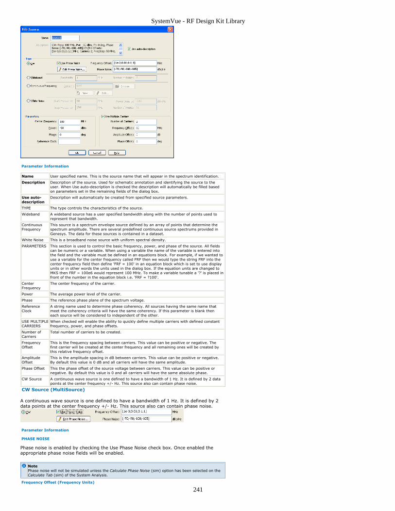
SystemVue - RF Design Kit Library
241
Parameter Information
Name User specified name. This is the source name that will appear in the spectrum identification.
Description Description of the source. Used for schematic annotation and identifying the source to theuser. When Use auto-description is checked the description will automatically be filled basedon parameters set in the remaining fields of the dialog box.
Use auto-description
Description will automatically be created from specified source parameters.
TYPE The type controls the characteristics of the source.
Wideband A wideband source has a user specified bandwidth along with the number of points used torepresent that bandwidth.
ContinuousFrequency
This source is a spectrum envelope source defined by an array of points that determine thespectrum amplitude. There are several predefined continuous source spectrums provided inGenesys. The data for these sources is contained in a dataset.
White Noise This is a broadband noise source with uniform spectral density.
PARAMETERS This section is used to control the basic frequency, power, and phase of the source. All fieldscan be numeric or a variable. When using a variable the name of the variable is entered intothe field and the variable must be defined in an equations block. For example, if we wanted touse a variable for the center frequency called FRF then we would type the string FRF into thecenter frequency field then define 'FRF = 100' in an equation block which is set to use displayunits or in other words the units used in the dialog box. If the equation units are changed toMKS then FRF = 100e6 would represent 100 MHz. To make a variable tunable a '?' is placed infront of the number in the equation block i.e. 'FRF = ?100'.
CenterFrequency
The center frequency of the carrier.
Power The average power level of the carrier.
Phase The reference phase plane of the spectrum voltage.
ReferenceClock
A string name used to determine phase coherency. All sources having the same name thatmeet the coherency criteria will have the same coherency. If this parameter is blank theneach source will be considered to independent of the other.
USE MULTIPLECARRIERS
When checked will enable the ability to quickly define multiple carriers with defined constantfrequency, power, and phase offsets.
Number ofCarriers
Total number of carriers to be created.
FrequencyOffset
This is the frequency spacing between carriers. This value can be positive or negative. Thefirst carrier will be created at the center frequency and all remaining ones will be created bythis relative frequency offset.
AmplitudeOffset
This is the amplitude spacing in dB between carriers. This value can be positive or negative.By default this value is 0 dB and all carriers will have the same amplitude.
Phase Offset This the phase offset of the source voltage between carriers. This value can be positive ornegative. By default this value is 0 and all carriers will have the same absolute phase.
CW Source A continuous wave source is one defined to have a bandwidth of 1 Hz. It is defined by 2 datapoints at the center frequency +/- Hz. This source also can contain phase noise.
CW Source (MultiSource)
A continuous wave source is one defined to have a bandwidth of 1 Hz. It is defined by 2data points at the center frequency +/- Hz. This source also can contain phase noise.
Parameter Information
PHASE NOISE
Phase noise is enabled by checking the Use Phase Noise check box. Once enabled theappropriate phase noise fields will be enabled.
NotePhase noise will not be simulated unless the Calculate Phase Noise (sim) option has been selected on theCalculate Tab (sim) of the System Analysis.
Frequency Offset (Frequency Units)

SystemVue - RF Design Kit Library
242
This is an array of frequency offsets from the CW carrier center frequency. These will bethe frequencies at which the phase noise power will be defined. This array MUST bedefined as increasing frequency. The phase noise can be specified as a single sideband ora double sideband. For double sided definition the lower sideband will appear first in thearray of frequency offsets with the most negative number appearing as the left mostentry. The lower sideband is always specified with negative frequency offsets. The uppersideband is always specified with positive frequency offsets with the largest offset beingthe right most entry in the frequency offset array.
A variable may be used to specify the array of frequency offsets. A simple vector offrequency offsets is created using basic variable rules. The vector must begin with an openbracket followed by a semicolon delimited vector array followed by a close bracket.
Phase Noise (dBc/Hz)
This is an array of power levels of the phase noise specified with respect to the CW carrierin a 1 Hz bandwidth. There must be a phase noise entry corresponding to every frequencyoffset entry. Values can be specified as positive or negative however, the phase noise willalways be below the carrier. A variable may be used to specify the array of phase noisevalues.
Edit Phase Noise Button
This is a simple wizard to assist the user in specifying the frequency offset phase noisepairs.
Phase Noise Edit Dialog
This dialog is used to edit the phase noise.
Parameter Information
FrequencyOffset(FrequencyUnits)
This is a list of offset frequencies from the carrier at which the phase noise will be specified.The phase noise frequency offsets can be specified either double sided or single sided. Thefrequency offsets must be specified in ascending order where the smallest or most negativefrequency is specified first. If only one sideband is specified it will be duplicated for the otherside when the actual carrier is created.
Phase Noise(dBm/Hz)
A phase noise value is specified for each of the frequency offsets. There must be a one toone correspondence. Every phase noise entry is assumed to be below the carrier. All entrieswill be converted in such a way to enforce this rule. There is no way that the phase noise canbe specified above the carrier.
Add, RemoveButtons
These buttons are used to add and remove rows in the table.
Up and DownButtons
These buttons are used to move a row up or down in the table. Select the row and use thesebuttons to move the row.
Wideband Source (MultiSource)
A wideband source has a user specified bandwidth along with the number of points usedto represent that bandwidth.
Parameter Information
Bandwidth(FrequencyUnits)
This is bandwidth of the source.
Number of Points This is the number of points used to be uniformly distributed across the carrier when it iscreated. When a wideband carrier passes through filtering stages additional noise pointsmay be needed to accurately represent the shape of the carrier.
Continuous Frequency Source (MultiSource)
This source is a spectrum envelope source defined by arrays of points that determine thespectrum amplitude and frequency. The data for these sources is contained in a dataset.These source datasets can be saved in libraries and used by various users. When a newsource is create the dataset will be added to the workspace tree expect for the internalsources supplied with Genesys. These internal sources are used by the system simulator

SystemVue - RF Design Kit Library
243
transparent to the user. However, once a source is edited it will be added to theworkspace tree.
Parameter Information
Dataset This is the name of the dataset that contains the continuous source spectrum data. The format is'DatasetName@Library'. If the internal dataset source library is used or the dataset resides in theworkspace tree then only the DatasetName is needed otherwise the full name and library arerequired.
BrowseButton
Click this button to select a continuous frequency source from a list of those contained in theworkspace and those provided internally. The selected name will appear in the dataset property.
NewButton
Click this button to create a new continuous source dataset. The new continuous source wizard willbe opened and user can fill in the necessary information to create a new dataset.
EditButton
Click this button to edit the specified source. When editing an internal source a new source will becreated and added to the workspace tree. Internal source datasets cannot be edited by the user.
NOTE: For internal sources the dataset wont be visible to the user unless it is imported intothe workspace.
Continuous Frequency Source Envelope Definition Dialog
This dialog is used to create or edit a source that is defined by its envelope.
Parameter Information
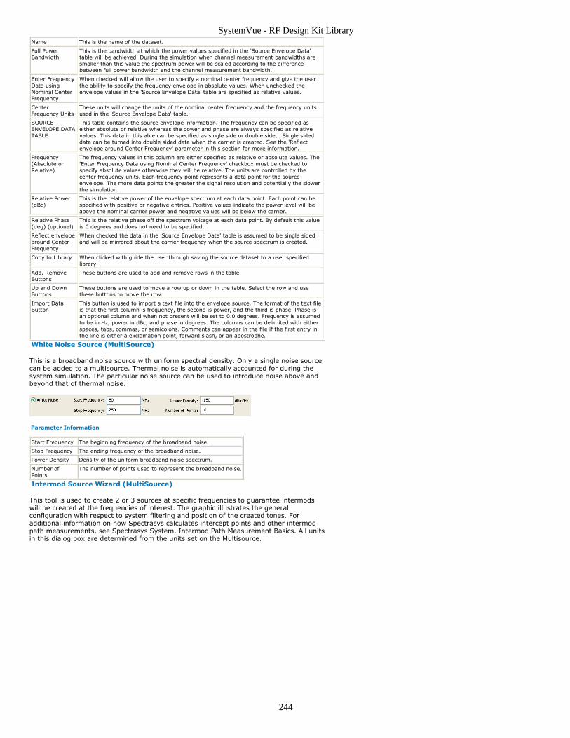
SystemVue - RF Design Kit Library
244
Name This is the name of the dataset.
Full PowerBandwidth
This is the bandwidth at which the power values specified in the 'Source Envelope Data'table will be achieved. During the simulation when channel measurement bandwidths aresmaller than this value the spectrum power will be scaled according to the differencebetween full power bandwidth and the channel measurement bandwidth.
Enter FrequencyData usingNominal CenterFrequency
When checked will allow the user to specify a nominal center frequency and give the userthe ability to specify the frequency envelope in absolute values. When unchecked theenvelope values in the 'Source Envelope Data' table are specified as relative values.
CenterFrequency Units
These units will change the units of the nominal center frequency and the frequency unitsused in the 'Source Envelope Data' table.
SOURCEENVELOPE DATATABLE
This table contains the source envelope information. The frequency can be specified aseither absolute or relative whereas the power and phase are always specified as relativevalues. This data in this able can be specified as single side or double sided. Single sideddata can be turned into double sided data when the carrier is created. See the 'Reflectenvelope around Center Frequency' parameter in this section for more information.
Frequency(Absolute orRelative)
The frequency values in this column are either specified as relative or absolute values. The'Enter Frequency Data using Nominal Center Frequency' checkbox must be checked tospecify absolute values otherwise they will be relative. The units are controlled by thecenter frequency units. Each frequency point represents a data point for the sourceenvelope. The more data points the greater the signal resolution and potentially the slowerthe simulation.
Relative Power(dBc)
This is the relative power of the envelope spectrum at each data point. Each point can bespecified with positive or negative entries. Positive values indicate the power level will beabove the nominal carrier power and negative values will be below the carrier.
Relative Phase(deg) (optional)
This is the relative phase off the spectrum voltage at each data point. By default this valueis 0 degrees and does not need to be specified.
Reflect envelopearound CenterFrequency
When checked the data in the 'Source Envelope Data' table is assumed to be single sidedand will be mirrored about the carrier frequency when the source spectrum is created.
Copy to Library When clicked with guide the user through saving the source dataset to a user specifiedlibrary.
Add, RemoveButtons
These buttons are used to add and remove rows in the table.
Up and DownButtons
These buttons are used to move a row up or down in the table. Select the row and usethese buttons to move the row.
Import DataButton
This button is used to import a text file into the envelope source. The format of the text fileis that the first column is frequency, the second is power, and the third is phase. Phase isan optional column and when not present will be set to 0.0 degrees. Frequency is assumedto be in Hz, power in dBc, and phase in degrees. The columns can be delimited with eitherspaces, tabs, commas, or semicolons. Comments can appear in the file if the first entry inthe line is either a exclamation point, forward slash, or an apostrophe.
White Noise Source (MultiSource)
This is a broadband noise source with uniform spectral density. Only a single noise sourcecan be added to a multisource. Thermal noise is automatically accounted for during thesystem simulation. The particular noise source can be used to introduce noise above andbeyond that of thermal noise.
Parameter Information
Start Frequency The beginning frequency of the broadband noise.
Stop Frequency The ending frequency of the broadband noise.
Power Density Density of the uniform broadband noise spectrum.
Number ofPoints
The number of points used to represent the broadband noise.
Intermod Source Wizard (MultiSource)
This tool is used to create 2 or 3 sources at specific frequencies to guarantee intermodswill be created at the frequencies of interest. The graphic illustrates the generalconfiguration with respect to system filtering and position of the created tones. Foradditional information on how Spectrasys calculates intercept points and other intermodpath measurements, see Spectrasys System, Intermod Path Measurement Basics. All unitsin this dialog box are determined from the units set on the Multisource.

SystemVue - RF Design Kit Library
245
Parameter Information
TYPE OFMEASUREMENT
This parameter determines whether 2 or 3 tones are created by the wizard. Two tones arecreated for an 'In-Band' type of measurement whereas three tones are created for an 'Out-of'Band' type of measurement.
In Band In this measurement it is assumed that the two tones are not attenuated significantlythrough the system since Spectrasys must measure the output power level of one of thesetones to determine the correct intercept point power level.
Out of Band In this measurement the two tones may be attenuated though filtering in the system likean IF of a receiver. In this case a 3 tone is created which is a small test tone injected atthe intermod frequency to determine the in-channel cascaded gain. Knowing the powerlevel of the two interfering tones to the system plus the in-channel cascaded gain a virtualtone power can be determined at the output of the system which will be used to find theintercept point. In the laboratory this would be done in a two step process since aspectrum analyzer is unable to separate out the cascaded gain test signal and theintermod. However, in Spectrasys this presents no problems and both signal can co-existat the same time.
LOCATION WITHRESPECT TOTONES
This parameter determines the position of the intermod with respect to the two tones.
Above The intermod to be measured is at a higher frequency than either of the tones.
Below The intermod to be measured is at a lower frequency than either of the tones.
Order ofIntermod (A)
This is the order of the intermod to be measured. Only odd orders are supported. Theapplies to intermod 'A' shown in the graphic.
Frequency ofIntermod toMeasure (A)
This is the absolute frequency of the intermod to be measured. The path channel frequencymust be set to this frequency to measure the power level of the intermod. This applies tointermod 'A' shown in the graphic.
2-Tone Spacing(Delta)
This is the desired spacing between the two tones. The frequency of the actual two tones isdetermined from the intermod order, 2-tone spacing, and position of the intermod withrespect to the 2-tones. This applies to the 'Delta' shown in the graphic.
2-Tone Amplitude(B)
This is the desired power level of both of the 2-tones. 'B' represents the power of bothtones in the graphic.
In-Channel TestTone Amplitude(A)
This is the power level of the test signal that will be created when the 'Out of Band' type ofmeasurement is selected. The test signal will be created at the same frequency of theintermod to determine the in-channel cascaded gain. This amplitude is not that importantbut must be set high enough so the test signal will not be thrown away during thesimulation. However, the amplitude should be set low enough not to cause stages to gointo compression. This test signal will appear at the same location as the intermod 'A'shown in the graphic.
Info Window This window summarizes the frequencies and power levels of all the signals that will becreated along with the information needed to setup the Spectrasys path correctly.

SystemVue - RF Design Kit Library
246
Transformer(Ruthroff) Part Ruthroff Transformer
Categories: T-Line (rfdesign)
The models associated with this part are listed below. To view detailed information on amodel (description, parameters, equations, notes, etc.), please click the appropriate link.
Model
TRFRUTH (rfdesign)

SystemVue - RF Design Kit Library
247
TRFRUTH
Description: Ruthroff TransformerAssociated Parts: Transformer(Ruthroff) Part (rfdesign)
Model Parameters
Name Description Default Units Type Runtime Tunable
N Number of Turns 1 none Float NO
AL Inductance Index (nH per turn2) 10 nH Float NO
Z Transmission Line Zo 100 ohm Float NO
L Electrical Line Length (deg) 90 deg Float NO
F Frequency for Electrical Length 500 MHz Float NO
Notes and Equations
Netlist Syntax:1.TRFRUTH n1 n2 n3 N= AL= Z= L= F=[Name=]Example:2.TRFRUTH 1 2 3 N=1 AL=1 Z=2 L=45 F=1000This is an ideal model based on the paper by Ruthroff. The shunt inductance is given3.by:L = N2*AL.Default SPICE Translation:4.XFERRUTH N=N AL=AL Z=Z E=L F=FSPICE Translation:5.None
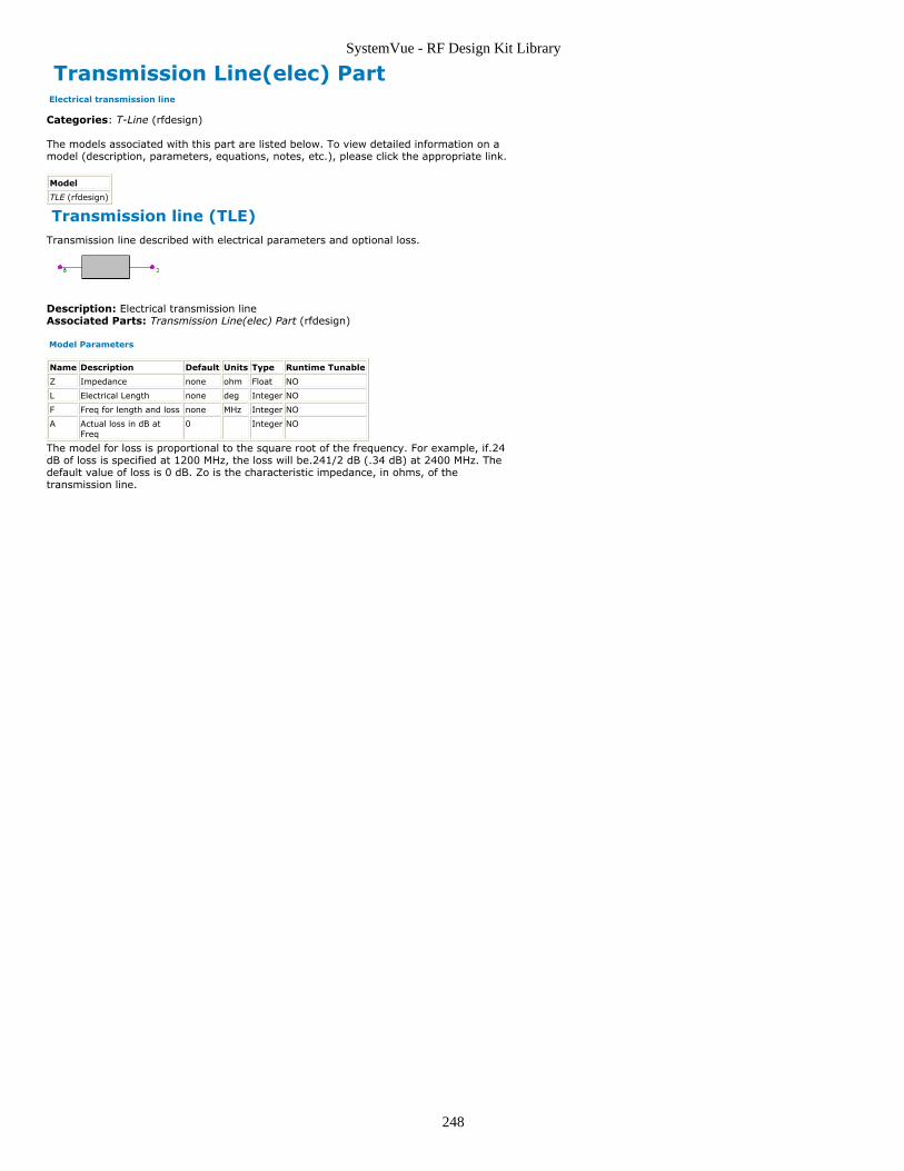
SystemVue - RF Design Kit Library
248
Transmission Line(elec) Part Electrical transmission line
Categories: T-Line (rfdesign)
The models associated with this part are listed below. To view detailed information on amodel (description, parameters, equations, notes, etc.), please click the appropriate link.
Model
TLE (rfdesign)
Transmission line (TLE)Transmission line described with electrical parameters and optional loss.
Description: Electrical transmission lineAssociated Parts: Transmission Line(elec) Part (rfdesign)
Model Parameters
Name Description Default Units Type Runtime Tunable
Z Impedance none ohm Float NO
L Electrical Length none deg Integer NO
F Freq for length and loss none MHz Integer NO
A Actual loss in dB atFreq
0 Integer NO
The model for loss is proportional to the square root of the frequency. For example, if.24dB of loss is specified at 1200 MHz, the loss will be.241/2 dB (.34 dB) at 2400 MHz. Thedefault value of loss is 0 dB. Zo is the characteristic impedance, in ohms, of thetransmission line.


