+ All Categories
Home > Documents > RF LDMOS Wideband Integrated Power Amplifiers ... · A3I35D025WNR1 A3I35D025WGNR1 Figure 4....

RF LDMOS Wideband Integrated Power Amplifiers ... · A3I35D025WNR1 A3I35D025WGNR1 Figure 4....

Date post: 31-May-2020
Category:
Upload: others
View: 13 times
Download: 0 times
Share this document with a friend
18
RF LDMOS Wideband Integrated Power Amplifiers The A3I35D025WN wideband integrated circuit is designed for cellular base station applications requiring very wide instantaneous bandwidth capability. This circuit includes on--chip matching that makes it usable from 3200 to 4000 MHz. Its multi--stage structure is rated for 20 to 32 V operation and covers all typical cellular base station modulation formats. 3500 MHz Typical Single--Carrier W--CDMA Characterization Performance: V DD = 28 Vdc, I DQ1(A+B) = 72 mA, I DQ2(A+B) = 260 mA, P out = 3.4 W Avg., Input Signal PAR = 9.9 dB @ 0.01% Probability on CCDF. (1) Frequency G ps (dB) PAE (%) ACPR (dBc) 3400 MHz 28.5 16.5 –46.5 3500 MHz 28.8 17.0 –46.3 3600 MHz 28.9 17.3 –46.1 3700 MHz 28.7 17.7 –46.4 3800 MHz 28.5 17.9 –46.2 Features Designed for wide instantaneous bandwidth applications On--chip matching (50 ohm input, DC blocked) Integrated quiescent current temperature compensation with enable/disable function (2) Designed for digital predistortion error correction systems Optimized for Doherty applications 1. All data measured in fixture with device soldered to heatsink. 2. Refer to AN1977, Quiescent Current Thermal Tracking Circuit in the RF Integrated Circuit Family, and to AN1987, Quiescent Current Control for the RF Integrated Circuit Device Family. Go to http://www.nxp.com/RF and search for AN1977 or AN1987. Document Number: A3I35D025WN Rev. 0, 06/2018 NXP Semiconductors Technical Data 3200–4000 MHz, 3.4 W AVG., 28 V AIRFAST RF LDMOS WIDEBAND INTEGRATED POWER AMPLIFIERS A3I35D025WNR1 A3I35D025WGNR1 TO--270WB--17 PLASTIC A3I35D025WN TO--270WBG--17 PLASTIC A3I35D025WGN 2018 NXP B.V.
Transcript

A3I35D025WNR1 A3I35D025WGNR1

1RF Device DataNXP Semiconductors

RF LDMOS Wideband IntegratedPower AmplifiersThe A3I35D025WN wideband integrated circuit is designed for cellular base

station applications requiring very wide instantaneous bandwidth capability.This circuit includes on--chip matching that makes it usable from 3200 to 4000MHz. Its multi--stage structure is rated for 20 to 32 V operation and covers alltypical cellular base station modulation formats.

3500 MHz

Typical Single--Carrier W--CDMA Characterization Performance:VDD = 28 Vdc, IDQ1(A+B) = 72 mA, IDQ2(A+B) = 260 mA, Pout = 3.4 W Avg.,Input Signal PAR = 9.9 dB @ 0.01% Probability on CCDF. (1)

FrequencyGps(dB)

PAE(%)

ACPR(dBc)

3400 MHz 28.5 16.5 –46.5

3500 MHz 28.8 17.0 –46.3

3600 MHz 28.9 17.3 –46.1

3700 MHz 28.7 17.7 –46.4

3800 MHz 28.5 17.9 –46.2

Features Designed for wide instantaneous bandwidth applications On--chip matching (50 ohm input, DC blocked) Integrated quiescent current temperature compensation with

enable/disable function (2)

Designed for digital predistortion error correction systems Optimized for Doherty applications

1. All data measured in fixture with device soldered to heatsink.2. Refer to AN1977, Quiescent Current Thermal Tracking Circuit in the RF Integrated Circuit Family, and to AN1987, Quiescent Current

Control for the RF Integrated Circuit Device Family. Go to http://www.nxp.com/RF and search for AN1977 or AN1987.

Document Number: A3I35D025WNRev. 0, 06/2018

NXP SemiconductorsTechnical Data

3200–4000 MHz, 3.4 W AVG., 28 VAIRFAST RF LDMOS WIDEBAND

INTEGRATED POWER AMPLIFIERS

A3I35D025WNR1A3I35D025WGNR1

TO--270WB--17PLASTIC

A3I35D025WN

TO--270WBG--17PLASTIC

A3I35D025WGN

2018 NXP B.V.

2RF Device Data

NXP Semiconductors

A3I35D025WNR1 A3I35D025WGNR1

Figure 1. Functional Block Diagram Figure 2. Pin Connections

Note: Exposed backside of the package isthe source terminal for the transistor.

Quiescent CurrentTemperature Compensation (1)

VDS1A

RFinA

VGS1A

RFout1/VDS2A

VGS2A

Quiescent CurrentTemperature Compensation (1)

VDS1B

RFinB

VGS1B

RFout2/VDS2B

VGS2B

VBWA

VBWB

VDS1A

RFinA

N.C.

RFinB

RFout1/VDS2A

1

234

78

15

VGS1B91011

VGS2AVGS1A

N.C.

N.C.

VGS2B

N.C.

VDS1B

RFout2/VDS2B

13

6

12

(Top View)

5

14

N.C.

16

17VBWA(4)

VBWB(4)

(3)(2)

1. Refer to AN1977, Quiescent Current Thermal Tracking Circuit in the RF IntegratedCircuit Family, and to AN1987,Quiescent Current Control for theRF IntegratedCircuitDevice Family. Go to http://www.nxp.com/RF and search for AN1977 or AN1987.

2. Pin connections 1 and 12 are DC coupledand RF independent.

3. Pin connections 14 and 16areDCcoupledand RF independent.

4. Device can operate with VDD currentsupplied through pin 13 and pin 17.

Table 1. Maximum Ratings

Rating Symbol Value Unit

Drain--Source Voltage VDSS –0.5, +65 Vdc

Gate--Source Voltage VGS –0.5, +10 Vdc

Operating Voltage VDD 32, +0 Vdc

Storage Temperature Range Tstg –65 to +150 C

Case Operating Temperature Range TC –40 to +150 C

Operating Junction Temperature Range (5,6) TJ –40 to +225 C

Input Power Pin 28 dBm

Table 2. Thermal Characteristics

Characteristic Symbol Value (6,7) Unit

Thermal Resistance, Junction to CaseCase Temperature 70C, 3.4 W, 3600 MHzStage 1, 28 Vdc, IDQ1(A+B) = 64 mAStage 2, 28 Vdc, IDQ2(A+B) = 260 mA

RJC

5.61.7

C/W

Table 3. ESD Protection Characteristics

Test Methodology Class

Human Body Model (per JS--001--2017) 1A

Charge Device Model (per JS--002--2014) C1

Table 4. Moisture Sensitivity Level

Test Methodology Rating Package Peak Temperature Unit

Per JESD22--A113, IPC/JEDEC J--STD--020 3 260 C

5. Continuous use at maximum temperature will affect MTTF.6. MTTF calculator available at http://www.nxp.com/RF/calculators.7. Refer to AN1955, Thermal Measurement Methodology of RF Power Amplifiers. Go to http://www.nxp.com/RF and search for AN1955.

A3I35D025WNR1 A3I35D025WGNR1

3RF Device DataNXP Semiconductors

Table 5. Electrical Characteristics (TA = 25C unless otherwise noted)

Characteristic Symbol Min Typ Max Unit

Stage 1 -- Off Characteristics

Zero Gate Voltage Drain Leakage Current (1)

(VDS = 65 Vdc, VGS = 0 Vdc)IDSS — — 10 Adc

Zero Gate Voltage Drain Leakage Current (1)

(VDS = 32 Vdc, VGS = 0 Vdc)IDSS — — 5 Adc

Gate--Source Leakage Current (2)

(VGS = 1.5 Vdc, VDS = 0 Vdc)IGSS — — 1 Adc

Stage 1 -- On Characteristics

Gate Threshold Voltage (2)

(VDS = 10 Vdc, ID = 3 Adc)VGS(th) 1.9 2.3 2.7 Vdc

Gate Quiescent Voltage(VDS = 28 Vdc, IDQ1(A+B) = 72 mAdc)

VGS(Q) — 3.6 — Vdc

Fixture Gate Quiescent Voltage(VDD = 28 Vdc, IDQ1(A+B) = 72 mAdc, Measured in Functional Test)

VGG(Q) 6.0 7.2 8.0 Vdc

Stage 2 -- Off Characteristics

Zero Gate Voltage Drain Leakage Current (1)

(VDS = 65 Vdc, VGS = 0 Vdc)IDSS — — 10 Adc

Zero Gate Voltage Drain Leakage Current (1)

(VDS = 32 Vdc, VGS = 0 Vdc)IDSS — — 5 Adc

Gate--Source Leakage Current (2)

(VGS = 1.5 Vdc, VDS = 0 Vdc)IGSS — — 1 Adc

Stage 2 -- On Characteristics

Gate Threshold Voltage (2)

(VDS = 10 Vdc, ID = 18 Adc)VGS(th) 1.9 2.3 2.7 Vdc

Gate Quiescent Voltage(VDS = 28 Vdc, IDQ2(A+B) = 260 mAdc)

VGS(Q) — 2.8 — Vdc

Fixture Gate Quiescent Voltage(VDD = 28 Vdc, IDQ2(A+B) = 260 mAdc, Measured in Functional Test)

VGG(Q) 5.0 5.5 6.0 Vdc

Drain--Source On--Voltage (1)

(VGS = 10 Vdc, ID = 360 mAdc)VDS(on) 0.05 0.16 0.3 Vdc

1. Side A and Side B are tied together for these measurements.2. Each side of device measured separately.

(continued)

4RF Device Data

NXP Semiconductors

A3I35D025WNR1 A3I35D025WGNR1

Table 5. Electrical Characteristics (TA = 25C unless otherwise noted) (continued)

Characteristic Symbol Min Typ Max Unit

Functional Tests (1,2,3) (In NXP Production Test Fixture, 50 ohm system) VDD = 28 Vdc, IDQ1(A+B) = 72 mA, IDQ2(A+B) = 260 mA,Pout = 3.4 W Avg., f = 3600 MHz, Single--Carrier W--CDMA, IQ Magnitude Clipping, Input Signal PAR = 9.9 dB @ 0.01% Probability onCCDF. ACPR measured in 3.84 MHz Channel Bandwidth @ 5 MHz Offset.

Power Gain Gps 26.5 28.9 30.5 dB

Power Added Efficiency PAE 15.5 17.3 — %

Adjacent Channel Power Ratio ACPR — –46.1 –42.5 dBc

Pout @ 3 dB Compression Point, CW P3dB 30.9 35.5 — W

Load Mismatch (In NXP Production Test Fixture, 50 ohm system) IDQ1(A+B) = 72 mA, IDQ2(A+B) = 260 mA, f = 3600 MHz

VSWR 10:1 at 32 Vdc, 34 W CW Output Power(3 dB Input Overdrive from 24 W CW Rated Power)

No Device Degradation

Typical Performance (4) (In NXP Characterization Test Fixture, 50 ohm system) VDD = 28 Vdc, IDQ1(A+B) = 72 mA, IDQ2(A+B) = 260 mA,3400–3800 MHz Bandwidth

Pout @ 3 dB Compression Point (5) P3dB — 35 — W

AM/PM(Maximum value measured at the P3dB compression point acrossthe 3400–3800 MHz frequency range.)

— –11 —

VBW Resonance Point(IMD Third Order Intermodulation Inflection Point)

VBWres — > 300 — MHz

Quiescent Current Accuracy over Temperature (6)

with 2.2 k Gate Feed Resistors (–30 to 85C) Stage 1with 2.2 k Gate Feed Resistors (–30 to 85C) Stage 2

IQT——

2.113.27

——

%

Gain Flatness in 400 MHz Bandwidth @ Pout = 3.4 W Avg. GF — 0.3 — dB

Gain Variation over Temperature(–40C to +85C)

G — 0.039 — dB/C

Output Power Variation over Temperature(–40C to +85C)

P1dB — 0.012 — dB/C

Table 6. Ordering Information

Device Tape and Reel Information Package

A3I35D025WNR1R1 Suffix = 500 Units, 44 mm Tape Width, 13--inch Reel

TO--270WB--17

A3I35D025WGNR1 TO--270WBG--17

1. The first stage drains (VDD1A andVDD1B) and second stagedrains (VDD2A andVDD2B)must be tied together and poweredby a singleDCpowersupply.

2. Part internally input and output matched.3. Measurements made with device in straight lead configuration before any lead forming operation is applied. Lead forming is used for gull

wing (GN) parts.4. All data measured in fixture with device soldered to heatsink.5. P3dB = Pavg + 7.0 dB where Pavg is the average output power measured using an unclipped W--CDMA single--carrier input signal where

output PAR is compressed to 7.0 dB @ 0.01% probability on CCDF.6. Refer to AN1977, Quiescent Current Thermal Tracking Circuit in the RF Integrated Circuit Family, and to AN1987, Quiescent Current

Control for the RF Integrated Circuit Device Family. Go to http://www.nxp.com/RF and search for AN1977 or AN1987.

A3I35D025WNR1 A3I35D025WGNR1

5RF Device DataNXP Semiconductors

Figure 3. A3I35D025WNR1 Production Test Circuit Component Layout

R3

C9 C10

C4C5C6

R6

R4

C25C18

R5

C12C17

C11C15 C1

C2C3C19

C7 C8R2

R1

C22

C24

C28

C21

C27

Z2

C23

C20C14

C26C16C13

VGG1A

VGG2A

VDD1A

VDD2A

VGG1B

VGG2B

VDD1B

VDD2B

A3I35D025WN

Rev. 6

CUTOUTAREA

Z1

Note: The first stage drains (VDD1A and VDD1B) and second stage drains (VDD2A and VDD2B) must be tiedtogether and powered by a single DC power supply.

Table 7. A3I35D025WNR1 Production Test Circuit Component Designations and ValuesPart Description Part Number Manufacturer

C1, C2, C3, C4, C5, C6, C7, C8, C9, C10,C11, C12, C13, C14

10 F Chip Capacitor C3225X7S1H106M250AB TDK

C15, C16, C17, C18 10 nF Chip Capacitor C0805C103K5RAC Kemet

C19, C20, C21, C22, C23, C24, C25, C26 3.3 pF Chip Capacitor ATC600S3R3BT250XT ATC

C27, C28 0.2 pF Chip Capacitor ATC600S0R2BT250XT ATC

R1, R2, R3, R4 2.2 k 1/8 W Chip Resistor CRCW08052K20JNEA Vishay

R5, R6 50 , 8 W Termination Chip Resistor C8A50Z4B Anaren

Z1, Z2 3300--3800 MHz Band, 90, 3 dB Hybrid Coupler X3C35F1-03S Anaren

PCB Taconic RF35A2, 0.020, r = 3.66 — MTL

6RF Device Data

NXP Semiconductors

A3I35D025WNR1 A3I35D025WGNR1

Figure 4. A3I35D025WNR1 Characterization Test Circuit Component Layout — 3400–3800 MHz

R3

C9 C10

C4C5C6

R6

R4

C25C18

R5

C12C17

C11C15

C1C2C3C19

C7 C8R2

R1

C22

C24

C28

C21 C27

Z2

C23

C20

Z1

C14 C26C16C13

VGG1A

VGG2A

VDD1A

VDD2A

VGG1B

VGG2B

VDD1B

VDD2B

D97408

A3I35D025WN

Rev. 6

Q1

Note 1: All data measured in fixture with device soldered to heatsink.Note 2: The first stage drains (VDD1A and VDD1B) and second stage drains (VDD2A and VDD2B) must be tied

together and powered by a single DC power supply.

C30

C29

Table 8. A3I35D025WNR1 Characterization Test Circuit Component Designations and Values — 3400–3800 MHzPart Description Part Number Manufacturer

C1, C2, C3, C4, C5, C6, C7, C8, C9, C10,C11, C12, C13, C14

10 F Chip Capacitor C3225X7S1H106M250AB TDK

C15, C16, C17, C18 10 nF Chip Capacitor C0805C103K5RAC Kemet

C19, C20, C21, C22, C23, C24, C25, C26 3.3 pF Chip Capacitor ATC600S3R3BT250XT ATC

C27, C28 0.2 pF Chip Capacitor ATC600S0R2BT250XT ATC

C29, C30 0.5 pF Chip Capacitor ATC600S0R5BT250XT ATC

Q1 RF Power LDMOS Transistor A3I35D025WN NXP

R1, R2, R3, R4 2.2 k 1/8 W Chip Resistor CRCW08052K20JNEA Vishay

R5, R6 50 , 8 W Termination Chip Resistor C8A50Z4B Anaren

Z1, Z2 3300--3800 MHz Band, 90, 3 dB Hybrid Coupler X3C35F1-03S Anaren

PCB Taconic RF35A2, 0.020, r = 3.66 D97408 MTL

A3I35D025WNR1 A3I35D025WGNR1

7RF Device DataNXP Semiconductors

Table 9. Load Pull Performance — Maximum Power TuningVDD = 28 Vdc, IDQ1(A) = 36 mA, IDQ2(A) = 130 mA, Pulsed CW, 10 sec(on), 10% Duty Cycle

f(MHz)

Zsource()

Zin()

Max Output Power

P1dB

Zload (1)

() Gain (dB) (dBm) (W)D(%)

AM/PM()

3200 78.0 – j14.9 80.6 + j7.43 17.9 – j24.2 27.6 42.1 16 50.5 –7

3400 60.6 + j14.4 60.6 – j15.9 20.1 – j19.5 28.1 42.1 16 50.7 –3

3600 47.3 + j7.35 54.7 – j8.11 16.3 – j18.7 27.7 42.4 17 53.7 –3

3800 37.2 – j9.77 47.6 + j6.54 14.1 – j18.3 26.6 42.6 18 52.6 –3

4000 27.5 – j10.3 40.8 + j9.76 14.2 – j18.1 25.9 42.6 18 51.1 –6

f(MHz)

Zsource()

Zin()

Max Output Power

P3dB

Zload (2)

() Gain (dB) (dBm) (W)D(%)

AM/PM()

3200 78.0 – j14.9 78.1 + j4.47 16.9 – j23.9 25.4 43.0 20 52.3 –11

3400 60.6 + j14.4 57.7 – j15.1 19.3 – j21.4 25.9 42.9 20 52.1 –5

3600 47.3 + j7.35 51.6 – j6.64 16.5 – j20.7 25.5 43.2 21 54.5 –3

3800 37.2 – j9.77 44.4 + j8.20 14.4 – j19.6 24.5 43.3 21 52.7 –3

4000 27.5 – j10.3 37.9 + j12.7 15.0 – j19.2 23.8 43.2 21 50.6 –9

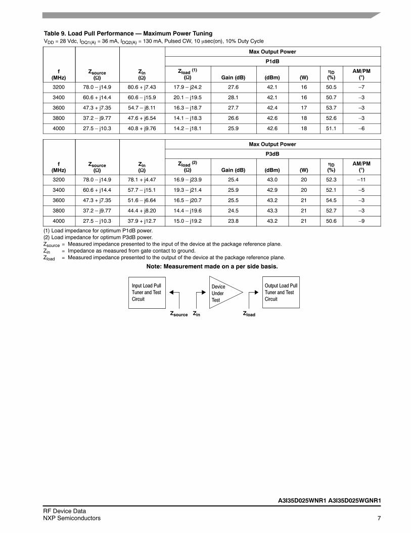
(1) Load impedance for optimum P1dB power.(2) Load impedance for optimum P3dB power.Zsource = Measured impedance presented to the input of the device at the package reference plane.Zin = Impedance as measured from gate contact to ground.Zload = Measured impedance presented to the output of the device at the package reference plane.

Note: Measurement made on a per side basis.

Input Load PullTuner and TestCircuit

DeviceUnderTest

Zsource Zin Zload

Output Load PullTuner and TestCircuit

8RF Device Data

NXP Semiconductors

A3I35D025WNR1 A3I35D025WGNR1

Table 10. Load Pull Performance — Maximum Efficiency TuningVDD = 28 Vdc, IDQ1(A) = 36 mA, IDQ2(A) = 130 mA, Pulsed CW, 10 sec(on), 10% Duty Cycle

f(MHz)

Zsource()

Zin()

Max Drain Efficiency

P1dB

Zload (1)

() Gain (dB) (dBm) (W)D(%)

AM/PM()

3200 78.0 – j14.9 89.3 + j9.63 31.4 – j22.6 28.9 41.2 13 55.7 –9

3400 60.6 + j14.4 64.5 – j22.5 26.7 – j8.05 29.3 41.1 13 56.4 –6

3600 47.3 + j7.35 57.7 – j16.2 15.1 – j6.90 28.7 41.0 12 59.2 –8

3800 37.2 – j9.77 48.5 + j0.17 12.3 – j11.0 27.5 41.6 15 58.1 –7

4000 27.5 – j10.3 40.6 + j2.95 9.72 – j12.6 26.8 41.7 15 56.2 –9

f(MHz)

Zsource()

Zin()

Max Drain Efficiency

P3dB

Zload (2)

() Gain (dB) (dBm) (W)D(%)

AM/PM()

3200 78.0 – j14.9 88.3 + j6.72 32.6 – j22.0 27.0 42.0 16 57.7 –14

3400 60.6 + j14.4 62.8 – j22.2 27.2 – j7.61 27.4 41.8 15 58.1 –9

3600 47.3 + j7.35 53.9 – j12.9 17.0 – j9.75 26.5 42.3 17 60.5 –8

3800 37.2 – j9.77 45.7 + j1.91 11.8 – j11.6 25.4 42.4 17 57.8 –7

4000 27.5 – j10.3 37.1 + j7.45 11.0 – j13.2 24.7 42.5 18 55.1 –12

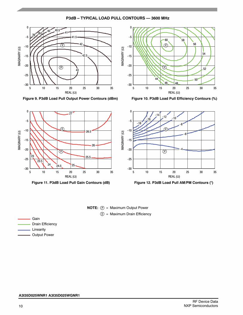
(1) Load impedance for optimum P1dB efficiency.(2) Load impedance for optimum P3dB efficiency.Zsource = Measured impedance presented to the input of the device at the package reference plane.Zin = Impedance as measured from gate contact to ground.Zload = Measured impedance presented to the output of the device at the package reference plane.

Note: Measurement made on a per side basis.

Input Load PullTuner and TestCircuit

DeviceUnderTest

Zsource Zin Zload

Output Load PullTuner and TestCircuit

A3I35D025WNR1 A3I35D025WGNR1

9RF Device DataNXP Semiconductors

P1dB – TYPICAL LOAD PULL CONTOURS — 3600 MHz

IMAGINARY()

155REAL ()

–3025

–25

3510 20 30

–20

–15

–10

–5

0

IMAGINARY()

155REAL ()

–3025

–25

3510 20 30

–20

–15

–10

–5

0IMAGINARY()

155REAL ()

–3025

–25

3510 20 30

–20

–15

–10

–5

0

IMAGINARY()

155REAL ()

–3025

–25

3510 20 30

–20

–15

–10

–5

0

NOTE: = Maximum Output Power

= Maximum Drain Efficiency

P

E

Gain

Drain Efficiency

Linearity

Output Power

Figure 5. P1dB Load Pull Output Power Contours (dBm) Figure 6. P1dB Load Pull Efficiency Contours (%)

Figure 7. P1dB Load Pull Gain Contours (dB) Figure 8. P1dB Load Pull AM/PM Contours ()

40.5

42

41.5

41

NOTE: = Maximum Output Power

= Maximum Drain Efficiency

P

E

Gain

Drain Efficiency

Linearity

Output Power

50

25

–16

4039 39.5

46

52

48

56

54

–18

38.5

44

58

25.5

–10–8

P

28.5

28

27.5

2726.526

E

–6

–4

P

E E

P

29

E

–14–12

P–2

46

10RF Device Data

NXP Semiconductors

A3I35D025WNR1 A3I35D025WGNR1

P3dB – TYPICAL LOAD PULL CONTOURS — 3600 MHz

IMAGINARY()

155REAL ()

–3025

–25

3510 20 30

–20

–15

–10

–5

0

IMAGINARY()

155REAL ()

–3025

–25

3510 20 30

–20

–15

–10

–5

0

IMAGINARY()

155REAL ()

–3025

–25

3510 20 30

–20

–15

–10

–5

0

IMAGINARY()

155REAL ()

–3025

–25

3510 20 30

–20

–15

–10

–5

0

NOTE: = Maximum Output Power

= Maximum Drain Efficiency

P

E

Gain

Drain Efficiency

Linearity

Output Power

Figure 9. P3dB Load Pull Output Power Contours (dBm) Figure 10. P3dB Load Pull Efficiency Contours (%)

Figure 11. P3dB Load Pull Gain Contours (dB) Figure 12. P3dB Load Pull AM/PM Contours ()

42.5

43

41.5

42

4140.540

52

54

50

5658

46

60

48

26.5

24

25.5

25

23

24.5

27

23.5

–16–14

–12 –10

–18

–6

P

E

39.5

44

–8

P

E

P

E

26

P

E

–4

39

A3I35D025WNR1 A3I35D025WGNR1

11RF Device DataNXP Semiconductors

PACKAGE DIMENSIONS

12RF Device Data

NXP Semiconductors

A3I35D025WNR1 A3I35D025WGNR1

A3I35D025WNR1 A3I35D025WGNR1

13RF Device DataNXP Semiconductors

14RF Device Data

NXP Semiconductors

A3I35D025WNR1 A3I35D025WGNR1

A3I35D025WNR1 A3I35D025WGNR1

15RF Device DataNXP Semiconductors

16RF Device Data

NXP Semiconductors

A3I35D025WNR1 A3I35D025WGNR1

A3I35D025WNR1 A3I35D025WGNR1

17RF Device DataNXP Semiconductors

PRODUCT DOCUMENTATION, SOFTWARE AND TOOLS

Refer to the following resources to aid your design process.

Application Notes AN1907: Solder Reflow Attach Method for High Power RF Devices in Plastic Packages

AN1955: Thermal Measurement Methodology of RF Power Amplifiers

AN1977: Quiescent Current Thermal Tracking Circuit in the RF Integrated Circuit Family

AN1987: Quiescent Current Control for the RF Integrated Circuit Device Family

Engineering Bulletins EB212: Using Data Sheet Impedances for RF LDMOS Devices

Software Electromigration MTTF Calculator

RF High Power Model

.s2p File

Development Tools Printed Circuit Boards

To Download Resources Specific to a Given Part Number:1. Go to http://www.nxp.com/RF

2. Search by part number

3. Click part number link

4. Choose the desired resource from the drop down menu

REVISION HISTORY

The following table summarizes revisions to this document.

Revision Date Description

0 June 2018 Initial release of data sheet

18RF Device Data

NXP Semiconductors

A3I35D025WNR1 A3I35D025WGNR1

Information in this document is provided solely to enable system and softwareimplementers to use NXP products. There are no express or implied copyright licensesgranted hereunder to design or fabricate any integrated circuits based on the informationin this document. NXP reserves the right to make changes without further notice to anyproducts herein.

NXP makes no warranty, representation, or guarantee regarding the suitability of itsproducts for any particular purpose, nor does NXP assume any liability arising out of theapplication or use of any product or circuit, and specifically disclaims any and all liability,including without limitation consequential or incidental damages. “Typical” parametersthat may be provided in NXP data sheets and/or specifications can and do vary indifferent applications, and actual performance may vary over time. All operatingparameters, including “typicals,” must be validated for each customer application bycustomer’s technical experts. NXP does not convey any license under its patent rightsnor the rights of others. NXP sells products pursuant to standard terms and conditions ofsale, which can be found at the following address: nxp.com/SalesTermsandConditions.

NXP, the NXP logo and Airfast are trademarks of NXP B.V. All other product or servicenames are the property of their respective owners.E 2018 NXP B.V.

How to Reach Us:

Home Page:nxp.com

Web Support:nxp.com/support

Document Number: A3I35D025WNRev. 0, 06/2018


Recommended