IEEE TRANSACTIONS ON ELECTRON DEVICES, VOL. 40, NO. 11, NOVEMBER 1993 I905 FtF Properties of Epitaxial Lift-off HEMT Devices Paul G. Young, Samuel A. Alterovitz, Rafael A. Mena, and Edwyn D. Smith, Senior Member, IEEE Abstract-Epitaxial layers containing GaAs HEMT and P-HEMT structures have been lifted-off the GaAs substrate and attached to other host substrates using an AlAs parting layer. The devices were on-wafer RF probed before and after the lift- off step showing no degradation in the measured S-parameters. The maximum stable gain indicates a low frequency enhance- ment of the gain of 1-2 dB with some devices showing an en- hancement of F,,,,,. FT consistently shows an increase of 12-20% for all lifted-off HEMT structures. Comparison of the Hall measurements and small signal models show that the gain is improved and this is most probably associated with an en- hanced carrier concentration. INTRODUCTION HE semiconductor device world is generally divided T up based on the type of material used. Each material has its own device advantages and applications; silicon with its MOS based technology, InP with its optical uses and microwave devices, GaAs with its microwave appli- cations, and insulating substrates for low RF losses. It would be advantageous to be able to integrate these dif- ferent material technologies on the same substrate and to interconnect the various devices without the use of bond wires. The epitaxial lift-off (ELO) process described be- low is one such approach. It has been demonstrated that an AlAs sacrificial layer buried between a GaAs substrate and an active device layer can be etched away allowing the micron thick active layer to be epitaxially lifted-off from the GaAs substrate for reattachment to a suitable substrate [ 13. The reattachment capability of the GaAs based E L 0 materials has made possible the integration of GaAs based, microwave MESFET’s and HEMT’s with many other materials [2]-[5]. The first demonstration of RF performance of an E L 0 transistor was done by Shah [2] using a GaAs film attached to silicon and transistor fab- rication being performed after ELO. The transistor exhib- ited a F,,, of 14 GHz for a 1.3 pm device. In our work, we published a short paper [5] showing an excellent RF result obtained on a finished HEMT device that was lifted off and attached to sapphire, with a F,,, of 31 GHz for a 1.2 pm device. The ideal scenario would be to first fabricate the de- vices and then reattach them to host substrates. This way, Manuscript received September 9, 1992; revised December 17, 1992. P. G. Young and E. D. Smith are with the Department of Electrical S. A. Alterovitz and R. A. Mena are with NASA Lewis Research Center, IEEE Log Number 9212312. The review of this paper was arranged by Associate Editor J. Xu. Engineering, University of Toledo, Toledo, OH 43606. Solid State Technology Branch, Cleveland, OH 44135. the FET processing does not interfere with the new sub- strate or possible existing circuits on the new host sub- strate as was demonstrated in our prior work [6] when we obtained a 10 GHz narrow-band amplifier using a peeled HEMT. In order to design circuits employing E L 0 de- vices, a characterization of the material parameters and microwave performance before and after E L 0 is required. The only prior electrical characterization E L 0 FET’s was done for the device DC properties [3], [4], [7] or on FET devices processed after the material was lifted off and de- posited on the new substrate [2]. This paper will present the results of the analysis of several HEMT structures before and after E L 0 trans- ferred to insulating substrates illustrating the effects of the EL0 step on the finished material and devices. The struc- tures characterized were a GaAs channel HEMT and a pseudomorphic InGaAs HEMT (P-HEMT) using devices fabricated before the E L 0 step. Microwave and material transport characterization were done to determine the change in device characteristics after ELO. EXPERIMENTAL The MBE grown wafers were Alo 3Gao ,As/GaAs/ Alo 3Gao ,AS and Alo 23Ga0.77A~ /Ino,2Gao,8As /GaAs P-HEMT hetrostructures supplied by QED Corporation. Both structures !se an undoped AlGaAs layer which is delta doped 50 A from the channel region using silicon impurity of concentration 3.5 X 10¹²/cm2. This structure reduces parallel conduction in the AlGaAs region and im- proves the Schottky contact performance. The structures yere grown on GaAs substrates (see Fig. 1) with a 500 A AlAs layer between the active layer and the GaAs sub- strate to enable the E L 0 process. Devices were fabricated using a 1500 A mesa etch pro- cedure for device isolation. Ohmic contacts were formed using standard metal liftoff of sequentially e-beam evap- orated Au/Ge/Au/Ni/Au contacts and alloyed for 15 s at 400°C. Gate recessing was performed after gate pho- tolithographic patterning to reduce the effects of parasitic gating of theo undoped wide bandgap material. Approxi- mately 150 A of AlGaAs was removed during the gate recessing step. A Ti/Au gate was e-beam evaporated after gate etching to form 0.8, 1.0, and 1.2 pm gate lengths and 200 pm gate widths. The transistor used a parallel gate finger structure with a source to drain separation of 4 pm. No passivation of the device was done. The lift-off process used an apiezon wax coating of ap- proximately 30 pm thickness [7]. The wax was cured at 0018-9383/93$03.00 0 1993 IEEE
Transcript
IEEE TRANSACTIONS ON ELECTRON DEVICES, VOL. 40, NO. 11, NOVEMBER 1993 I905
FtF Properties of Epitaxial Lift-off HEMT Devices Paul G. Young, Samuel A. Alterovitz, Rafael A. Mena, and Edwyn D. Smith, Senior Member, IEEE
Abstract-Epitaxial layers containing GaAs HEMT and P-HEMT structures have been lifted-off the GaAs substrate and attached to other host substrates using an AlAs parting layer. The devices were on-wafer RF probed before and after the lift- off step showing no degradation in the measured S-parameters. The maximum stable gain indicates a low frequency enhance- ment of the gain of 1-2 dB with some devices showing an en- hancement of F,,,,,. FT consistently shows an increase of 12-20% for all lifted-off HEMT structures. Comparison of the Hall measurements and small signal models show that the gain is improved and this is most probably associated with an en- hanced carrier concentration.
INTRODUCTION HE semiconductor device world is generally divided T up based on the type of material used. Each material
has its own device advantages and applications; silicon with its MOS based technology, InP with its optical uses and microwave devices, GaAs with its microwave appli- cations, and insulating substrates for low RF losses. It would be advantageous to be able to integrate these dif- ferent material technologies on the same substrate and to interconnect the various devices without the use of bond wires. The epitaxial lift-off (ELO) process described be- low is one such approach. It has been demonstrated that an AlAs sacrificial layer buried between a GaAs substrate and an active device layer can be etched away allowing the micron thick active layer to be epitaxially lifted-off from the GaAs substrate for reattachment to a suitable substrate [ 13.
The reattachment capability of the GaAs based E L 0 materials has made possible the integration of GaAs based, microwave MESFET’s and HEMT’s with many other materials [2]-[5]. The first demonstration of RF performance of an E L 0 transistor was done by Shah [2] using a GaAs film attached to silicon and transistor fab- rication being performed after ELO. The transistor exhib- ited a F,,, of 14 GHz for a 1.3 pm device. In our work, we published a short paper [5] showing an excellent RF result obtained on a finished HEMT device that was lifted off and attached to sapphire, with a F,,, of 31 GHz for a 1.2 pm device.
The ideal scenario would be to first fabricate the de- vices and then reattach them to host substrates. This way,
Manuscript received September 9, 1992; revised December 17, 1992.
P. G. Young and E. D. Smith are with the Department of Electrical
S. A. Alterovitz and R. A. Mena are with NASA Lewis Research Center,
IEEE Log Number 9212312.
The review of this paper was arranged by Associate Editor J . Xu.
Engineering, University of Toledo, Toledo, OH 43606.
Solid State Technology Branch, Cleveland, OH 44135.
the FET processing does not interfere with the new sub- strate or possible existing circuits on the new host sub- strate as was demonstrated in our prior work [6] when we obtained a 10 GHz narrow-band amplifier using a peeled HEMT. In order to design circuits employing E L 0 de- vices, a characterization of the material parameters and microwave performance before and after E L 0 is required. The only prior electrical characterization E L 0 FET’s was done for the device DC properties [3], [4], [7] or on FET devices processed after the material was lifted off and de- posited on the new substrate [2].
This paper will present the results of the analysis of several HEMT structures before and after E L 0 trans- ferred to insulating substrates illustrating the effects of the E L 0 step on the finished material and devices. The struc- tures characterized were a GaAs channel HEMT and a pseudomorphic InGaAs HEMT (P-HEMT) using devices fabricated before the E L 0 step. Microwave and material transport characterization were done to determine the change in device characteristics after ELO.
EXPERIMENTAL The MBE grown wafers were Alo 3Gao ,As/GaAs/
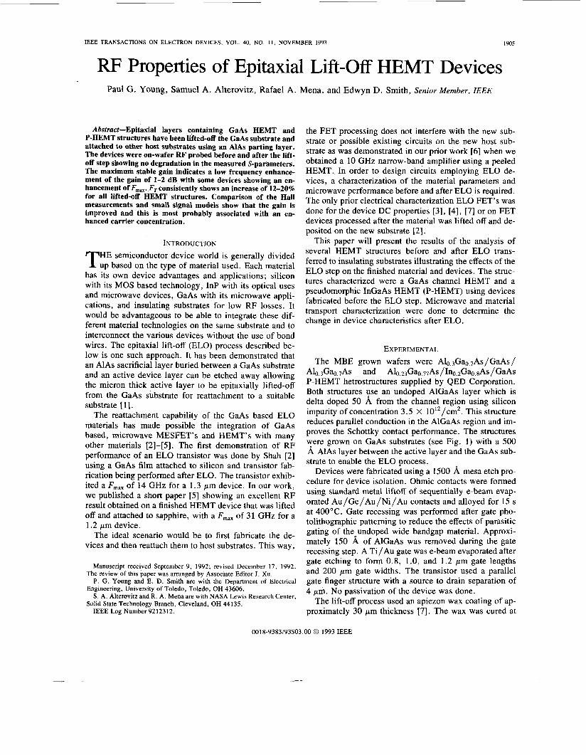
Alo 3Gao ,AS and Alo 23Ga0.77A~ /Ino,2Gao,8As /GaAs P-HEMT hetrostructures supplied by QED Corporation. Both structures !se an undoped AlGaAs layer which is delta doped 50 A from the channel region using silicon impurity of concentration 3.5 X 10¹²/cm2. This structure reduces parallel conduction in the AlGaAs region and im- proves the Schottky contact performance. The structures yere grown on GaAs substrates (see Fig. 1) with a 500 A AlAs layer between the active layer and the GaAs sub- strate to enable the E L 0 process.
Devices were fabricated using a 1500 A mesa etch pro- cedure for device isolation. Ohmic contacts were formed using standard metal liftoff of sequentially e-beam evap- orated Au/Ge/Au/Ni/Au contacts and alloyed for 15 s at 400°C. Gate recessing was performed after gate pho- tolithographic patterning to reduce the effects of parasitic gating of theo undoped wide bandgap material. Approxi- mately 150 A of AlGaAs was removed during the gate recessing step. A Ti/Au gate was e-beam evaporated after gate etching to form 0.8, 1.0, and 1.2 pm gate lengths and 200 pm gate widths. The transistor used a parallel gate finger structure with a source to drain separation of 4 pm. No passivation of the device was done.
The lift-off process used an apiezon wax coating of ap- proximately 30 pm thickness [7]. The wax was cured at
0018-9383/93$03.00 0 1993 IEEE
IEEE TRANSACTIONS ON ELECTRON DEVICES, VOL. 40, NO. 1 1 , NOVEMBER 1993 1906
n+ GaAs Capping L a y e r (350A)
A 1 o.s Gao.r As ( 375A)
Undoped GaAs Channe l R e g i o n (300A) ~
AlGaAslGaAs Super L a t t i c e (6900A)
AlAs Release Layer
SI GaAs S u b s t r a t e
I
undoped AlGaAs (50A) w i t h a d e l t a
~J doped S i l i c o n l a y e r O f 3.5e12/cm2
n+ GaAs Capping L a y e r (350A)
Alo.23Gao.nAs (375A)
undoped I ~ ~ , ~ G ~ ~ . ~ A ~ channel Region ( 1 5 0 ~ )
GaAs Layer and Super L a t t l c e (lum)
AlAs Release Layer
SI GaAs S u b s t r a t e
(b) Fig. 1 . (a) EL0 HEMT structure with a GaAs channel. (b) EL0 P-HEMT
structure.
undoped AlGaAs (50A) w i t h a d e l t a
doped S i l i c o n l a y e r 0 1 3 . 5 e i 2 / c m 2
150°C for 30 min to give a compressive force to the wax to help facilitate peel off. The sample edges were cleaned and subjected to a H202 : NH40H etch to remove the ac- tive layer leaving the AlAs layer exposed. The samples were then allowed to etch at room temperature in a DI : HF solution overnight where the active layer separated from the substrate and floated in the solution upon separation.
The films were then attached to sapphire of various ori- entations and quartz substrates using Van der Waals forces and, after 12 h, the wax was removed with trichloroeth- ylene (TCE). To improve adhesion the devices were coated with a spin-on glass (SOG) and cured at 250°C for 4 h. Hall bars were also transferred to quartz substrates to determine Hall mobilities and carrier density, and per- form Shubnikov-de Haas (SdH) measurements. Contact resistivities were determined using transmission line mea- surements.
Transistors were tested before and after E L 0 to make a one to one comparison of the same devices and to elim- inate the effects of fabrication variation within device lots. Testing of the devices was done on a HP 85 10B automatic network analyzer with Cascade Microtech RF probes for on wafer probing of the devices. The devices were tested at various gate voltages while maintaining a constant drain voltage. This insured that the device was operating at its peak transconductance and that any changes were not as- sociated with a charging effect.
RESULTS AND DISCUSSION The plots of maximum available gain G,,, are shown
for the two structures in Fig. 2. The gain plots show an approximate 1-2 dB enhancement in G,,, for the E L 0 devices vs. their performance before ELO. The improve- ment in low frequency gain indicates a possible increase in the intrinsic transconductance for both structures. This
40 I 30
h
D a x 20
0
v
2 10
0 1 10
Frequency (GHz)
(a)
1 10
Frequency (GHz)
(b) Fig. 2 . Before and after EL0 maximum available gain response for a
1.2 pm. (a) GaAs channel HEMT and (b) P-HEMT.
effect on G,,, appears to be consistent in all of the 20 devices measured.
In the case of the pseudomorphic structures shown, F,,, is enhanced by E L 0 while it is not changed as dramati- cally by EL0 for the GaAs channel structure. F,,, is de- pendent upon various capacitances, resistances and the in- trinsic transconductance [8]. Each device structure will experience slightly different variations in the capacitances and resistances due to material and processing variations after ELO. This multiple variable dependency and the small overall change in F,,, makes it difficult to distin- guish which individual parameter might be changing after E L 0 .
It should be noted that the enhancement of the gain and the effects of F,,, are not unique to the particular device fabrication lot. The testing was done on various transistor lots and there were similar results for different lots made of similar material. Some researchers have reported on actual degradation of extrinsic transconductance mea- sured for devices after E L 0 [7]. We found this to be also true in our initial E L 0 work, but was later traced to etch- ing of the exposed material between the gate and source/
YOUNG et al.: RF PROPERTIES OF EPITAXIAL HEMT DEVICES 1907
drain regions during peel off. Improving the coating pro- cess eliminated the device degradation.
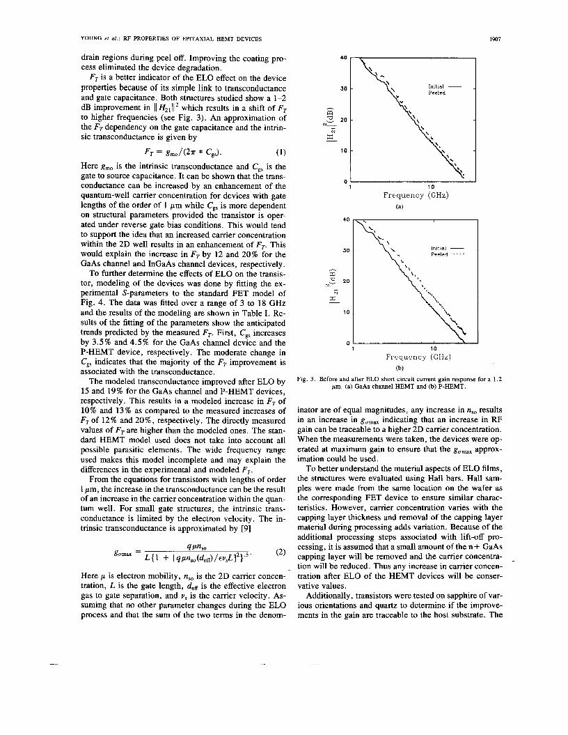
FT is a better indicator of the E L 0 effect on the device properties because of its simple link to transconductance and gate capacitance. Both structures studied show a 1-2 dB improvement in 11 H21112 which results in a shift of FT to higher frequencies (see Fig. 3). An approximation of the FT dependency on the gate capacitance and the intrin- sic transconductance is given by
(1) Here g,, is the intrinsic transconductance and C,, is the gate to source capacitance. It can be shown that the trans- conductance can be increased by an enhancement of the quantum-well carrier concentration for devices with gate lengths of the order of 1 pm while C,, is more dependent on structural parameters provided the transistor is oper- ated under reverse gate bias conditions. This would tend to support the idea that an increased carrier concentration within the 2D well results in an enhancement of FF This would explain the increase in FT by 12 and 20% for the GaAs channel and InGaAs channel devices, respectively.
To further determine the effects of E L 0 on the transis- tor, modeling of the devices was done by fitting the ex- perimental S-parameters to the standard FET model of Fig. 4. The data was fitted over a range of 3 to 18 GHz and the results of the modeling are shown in Table I . Re- sults of the fitting of the parameters show the anticipated trends predicted by the measured FT. First, C,, increases by 3.5 % and 4.5 % for the GaAs channel device and the P-HEMT device, respectively. The moderate change in Cg, indicates that the majority of the FT improvement is associated with the transconductance.
The modeled transconductance improved after E L 0 by 15 and 19% for the GaAs channel and P-HEMT devices, respectively. This results in a modeled increase in FT of 10% and 13% as compared to the measured increases of FT of 12 % and 20%, respectively. The directly measured values of FT are higher than the modeled ones. The stan- dard HEMT model used does not take into account all possible parasitic elements. The wide frequency range used makes this model incomplete and may explain the differences in the experimental and modeled FT.
From the equations for transistors with lengths of order 1 pm, the increase in the transconductance can be the result of an increase in the carrier concentration within the quan- tum well. For small gate structures, the intrinsic trans- conductance is limited by the electron velocity. The in- trinsic transconductance is approximated by [9]
FT = gmo/(2a * Cgs>.
Here p is electron mobility, nso is the 2D carrier concen- tration, L is the gate length, de, is the effective electron gas to gate separation, and v, is the carrier velocity. As- suming that no other parameter changes during the E L 0 process and that the sum of the two terms in the denom-
40
30
h
D z 20 CO- -
N 3: -
10
0
40
30
h
D z 20 N- ....
N 5: -
10
0
1 10
Frequency (GHz)
(a)
Initial - Peeled
l o Frequency (GHz)
(b) Fig. 3 . Before and after E L 0 short circuit current gain response for a 1.2
pm. (a) GaAs channel HEMT and (b) P-HEMT.
inator are of equal magnitudes, any increase in nso results in an increase in go,,, indicating that an increase in RF gain can be traceable to a higher 2D carrier concentration. When the measurements were taken, the devices were op- erated at maximum gain to ensure that the go,,, approx- imation could be used.
To better understand the material aspects of E L 0 films, the structures were evaluated using Hall bars. Hall sam- ples were made from the same location on the wafer as the corresponding FET device to ensure similar charac- teristics. However, carrier concentration varies with the capping layer thickness and removal of the capping layer material during processing adds variation. Because of the additional processing steps associated with lift-off pro- cessing, it is assumed that a small amount of the n+ GaAs capping layer will be removed and the carrier concentra- tion will be reduced. Thus any increase in carrier concen- tration after E L 0 of the HEMT devices will be conser- vative values.
Additionally, transistors were tested on sapphire of var- ious orientations and quartz to determine if the improve- ments in the gain are traceable to the host substrate. The
1908 IEEE TRANSACTIONS ON ELECTRON DEVICES, VOL. 40, NO. 11, NOVEMBER 1993
Gate Cdg
If Drain Gate
0 I Rds 7q Cds
T Cdc
Source
Fig. 4 . Small signal equivalent circuit model for a HEMT.
TABLE I SMALL SIGNAL EQUIVALENT CIRCUIT MODEL VALUES. *MEASURED F,
GaAs HEMT P-HEMT
Before After Before After
g m o (mS) 0.043 0.049 0.0265 0.032
(PO 0.405 0.412 0.3067 0.314 C*S
(PO 0.0234 0.0241 0.0237 0.021
1.16 * 1OI2/cm2 before and after ELO, respectively. The P-HEMT structure showed a similar shift of 1.78 * 1012/cm2 to 1.85 * 1012/cm2, respectively. The increase in the carrier concentration exists across the temperature range for both of the structures. In addition, a homoge- neously doped GaAs well and a channel doped GaAs well structures were tested resulting in similar carrier concen- tration increases. Electron mobilities were also measured as a function of temperature and no change in the mobility was detected down to 1.4 K indicating no additional scat- tering was generated during ELO.
To get further insight into the effects of ELO, SdH 0.0513 0.0401 0.0588 0.0331
(ohm) 12.02 12.20 8.10 8.20 measurements were conducted on the GaAs channel and the pseudomorphic structures. The SdH carrier concentra- tion for the GaAs channel increased from 0.936 *
(ohm) 519.9 511 556.6 550.5 10I2/cm2 to 1.03 * 10I2/cm2 after EL0 and the P-HEMT structure increased from 1.5 * 1012/cm2 to 1.65 * 1OI2 /cm2. The carrier concentrations as measured using (GHz)
R, 13.2 (ohm) 13.03 13.08 13.33
Rds
F T 26 29 23 30
quartz has a isotropic medium with a relative permittivity of 3.9 while sapphire is anisotropic with a permittivity in the optical plane being 11.6 and 9.4 in the perpendicular planes. Analysis of HZ1 before and after E L 0 using GaAs channel HEMT devices attached to quartz and sapphire substrates was done, and the change in the H21 was 1.3 f 0.1 dB. This would indicate that the gain and C,, are in- dependent of the host substrate and that change in gain would be attributed to an enhancement in the quantum carrier confinement. Thus, assuming that the host sub- strate permittivity does not effect the effective permittivity seen by the EL0 device and using (2), this would result in a 18% and 18.4% change in carrier concentration for the GaAs channel and P-HEMT devices, respectively.
Analysis of the Hall data shows an increase in carrier concentration by approximately 5% for both the struc- tures tested [ 101. The GaAs channel device showed a shift in carrier concentration at 1.4 K from 1.09 * 10l2 /cm2 to
the SdH techniques showed a 10% increase after E L 0 as compared to a 5 % increase using the Hall techniques at 1.4 K.
The Hall carrier concentration is the carrier concentra- tion of the total structure, inside and outside the quantum well, while the 2D carrier Concentration found from the SdH oscillations is restricted to quanitized regions created by the well. The Hall results indicate that the overall car- rier concentration is increased by 5 % after ELO, but more importantly, the confined carrier concentration within the 2D well increased by EL0 by 10%.
It is assumed that the increase in carrier concentration is associated with a decrease in the substrate leakage or possibly a back gating effect associated with the interface between the insulating host substrate and the E L 0 film layer. Further analysis of the possible back gating effect was conducted [lo] using a self consistent calculation of the energy subbands to explain the possibility of a charge build up or a potential generated at the interface between the host substrate and E L 0 layer. The model shows that
YOUNG et al.: RF PROPERTIES OF EPITAXIAL HEMT DEVICES 1909
a backgating voltage lowers the quantum states within the well and increases the number of carriers within the well. This appears to correlate with the measured increase in quantum-well carrier concentration measured with SdH measurements.
CONCLUSIONS
Characterization of quantum well structures before and after E L 0 has been presented here. The E L 0 transistors show a consistent increase in FT of between 12-20% and a low frequency increase in G,,, of 1-2 dB as measured by the S-parameters. An evaluation of the E L 0 structures indicates that there exists an increase in carrier confine- ment after lift-off resulting in a transconductance in- crease.
This evaluation of the E L 0 process for the two major HEMT structures permits a circuit designer to predict the effects of a transistor lift-off onto an insulating substrate. Finished devices or circuits can easily be removed from a host substrate and integrated into a device technology without degrading the active devices. Using this technol- ogy, the cost and circuit performance of GaAs based ac- tive devices can be enhanced by E L 0 processing to achieve integrated circuits of various device technologies on a single substrate.
REFERENCES
[l] M. Konagai, M. Sugimoto, and K. Takahashi, “High efficiency GaAs thin film cells by peeled film technology,” J . Cryst. Growth, vol. 45,
[2] D. M. Shah, W. K. Chan, T . J. Gmitter, L. T. Florez, H. Schu- macher, and B. P. Van der Gaag, “DC and RF performance of GaAs MESFET fabrication on silicon substrate using epitaxial lift-off tech- nique,” Electron. Lett., vol. 26, no. 22, pp. 1865-1866, Oct. 1990.
[3] W. K. Chan, D. M. Shah, T . J . Gmitter, and C . Caneau, “Inverted Gate GaAs MESFET by Epitaxial Liftoff,” Electron. Lett., vol. 28, no. 8, pp. 708-709, Apr. 1992.
[4] D. R. Myers, J . F. Klem, and J . A. Lott, “(A1Ga)AshGaAs strained- auantum-well FET’s on silicon dioxide be selective device lift-off as
pp. 277-280, 1978.
an alternative to hetroepitaxy,” IEDM, pp. 704-707, 1988. P. G. Young, S. A. Alterovitz, R. A. Mena, and E. D. Smith, “Mi- crowave properties of ‘peeled’ HEMT devices on sapphire sub- strates,” in Proc. 1991 Internat. Semiconductor Device Res. Symp., Charlottesville, VA, Dec. 1991, pp. 689-692. P. G. Young, R. R. Romanofsky, S. A. Alterovitz, and E. D. Smith, “X-band ‘peeled’ HEMT amplifier,” in Proc. SPIE 1992 Symp. Compound Semiconductor Physics and Devices, Somerset, NJ, pp.
C. Van Hoof, W. De Raedt, M. Van Rossum, and G. Borghs, “MES- FET lift-off from GaAs substrate to Glass host,” Electron. Lett., vol. 25, no. 2, pp. 136-137, Jan. 1989. M. H. Weiler and Y. Ayasli, “DC and microwave models for AI,Ga, -.As/GaAs high electron mobility transistors,” IEEE Trans. on Electron Device, vol. ED-31, pp. 1854-1861, Dec. 1984. M. Shur, GaAs Devices and Circuits. New York: Plenum, 1987, p. 565. R. A. Mena, S. E. Schacham, P. G. Young, and S. A. Alterovitz, “Transport properties of epitaxial lift-off materials,” J . Appl. Phys., to be published.
72-79.
Paul G. Young received the Ph.D. degree in 1992 from the University of Toledo, the M.S. degree from University of Cincinnati in 1987, and the B.S.E.E. degree from the University of Toledo in 1985.
From 1987 to 1990 he was employed by Hams/ RCA in the Solid State Division as a Technical Staff member. He has been active in the areas of 111-V compound semiconductor process develop- ment with an emphasis on InP self gate aligned MOSFET structures and GaAs MODFET struc-
tures. Presently, his research interests are in epitaxial liftoff MODFET de- vices and circuit, S i c MESFET’s for microwave applications, and cryo- genic on-wafer measurement of devices.
Samuel A. Alterovitz received the Ph.D. degree in solid state physics in 1971 from Tel Aviv Uni- versity, Israel.
After a 2-year postdoctoral appointment at the University of Illinois, Urbana, IL, he joined the staff of the Physics Department at Tel Aviv Uni- versity where he achieved the rank of tenured as- sociated professor. In both places he worked on properties of superconducting materials, espe- cially critical currents and critical fields. In 1981, he accepted a position in the Electrical Engineer-
ing Department at the University of Nebraska, Lincoln, NE, as senior en- gineering research scientist. In 1983, he transferred to NASA Lewis Re- search Center where he is now a senior research scientist. He played an important role in developing new materials (e.g., InGaAs) for high-speed, low-noise, high efficiency electronic devices. He also developed ellip- sometry for novel and multiplayer structures. He is now working on epi- taxial lift-off technique development, materials and devices for cryogenic electronics applications, and on further applications of the ellipsometric technique. He has authored over 120 papers in referred journals and over 100 meeting presentations and has edited five books. He is an active Na- tional Research Council postdoctoral adviser.
Dr. Alterovitz is a member of the American Physical Society, the Ma- terials Research Society and the American Vacuum Society.
Rafael A. Mena received the B.S. degree in elec- trical engineering in 1988 from the University of Texas at El Paso and the M.S. degree in electrical engineering in 1990 from Arizona State Univer- sity, Tempe.
While at Arizona State University, he carried out theoretical calculations on the effect of a mag- netic field on the optical properties of semicon- ductor alloys. In 1990, he joined the Solid State Technology Branch at NASA Lewis Research Center as a full-time employee. His current inter-
ests lie in both the theoretical and experimental investigation of the elec- trical properties of novel semiconductor materials.
Edwyn D. Smith (S’61-M’66-SM’90) received the B.S., M.S., and Ph.D. degrees from the Uni- versity of Arizona, Tucson, in 1961, 1963, and 1974 respectively.
From 1969 through 1972, he was employed as a test engineer by the Hughes Aircraft Company. From 1974 through 1981, he was with the U.S. Army Night Vision and Electro-Optics Labora- tory and the Stewart Observatory involved with low-light-level and thermal imaging systems. Since 1982, he has been an Associate Professor in
the Department of Electrical Engineering at the University of Toledo, To- ledo, OH, where he teaches courses and conducts research in VLSI and semiconductor devices.