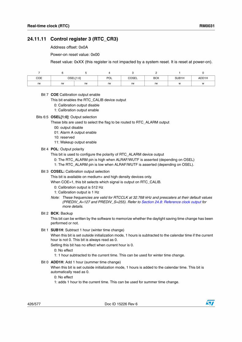
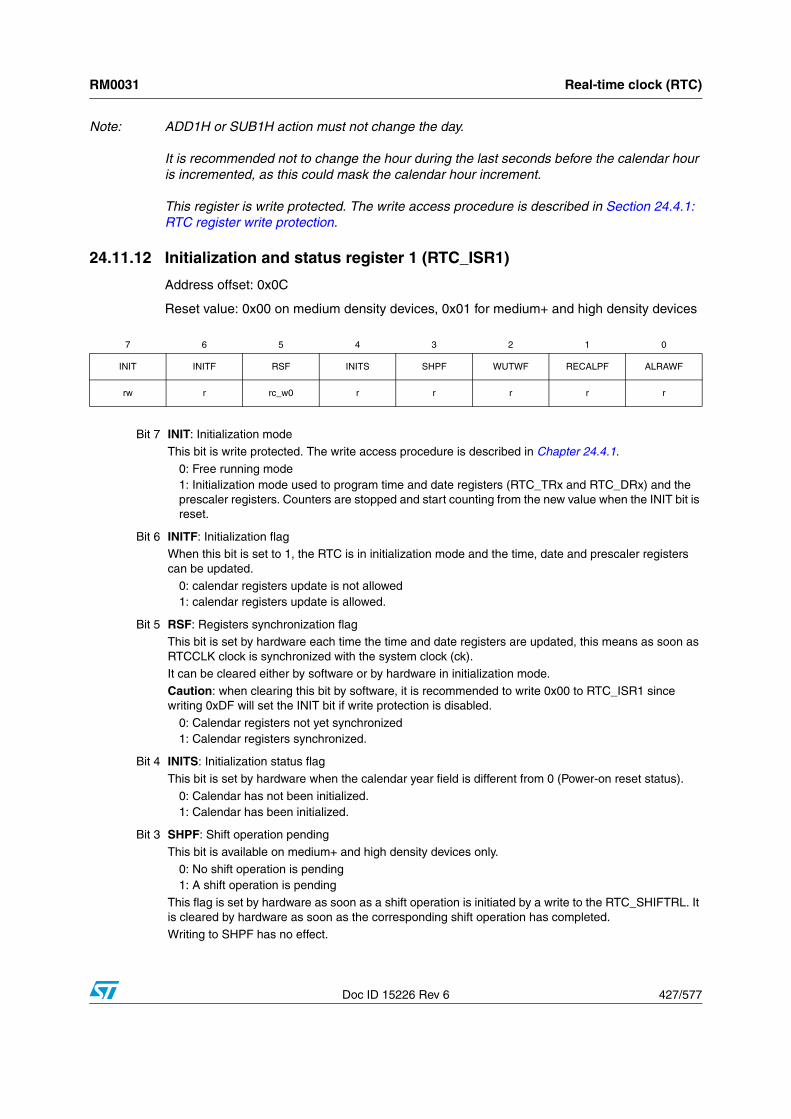
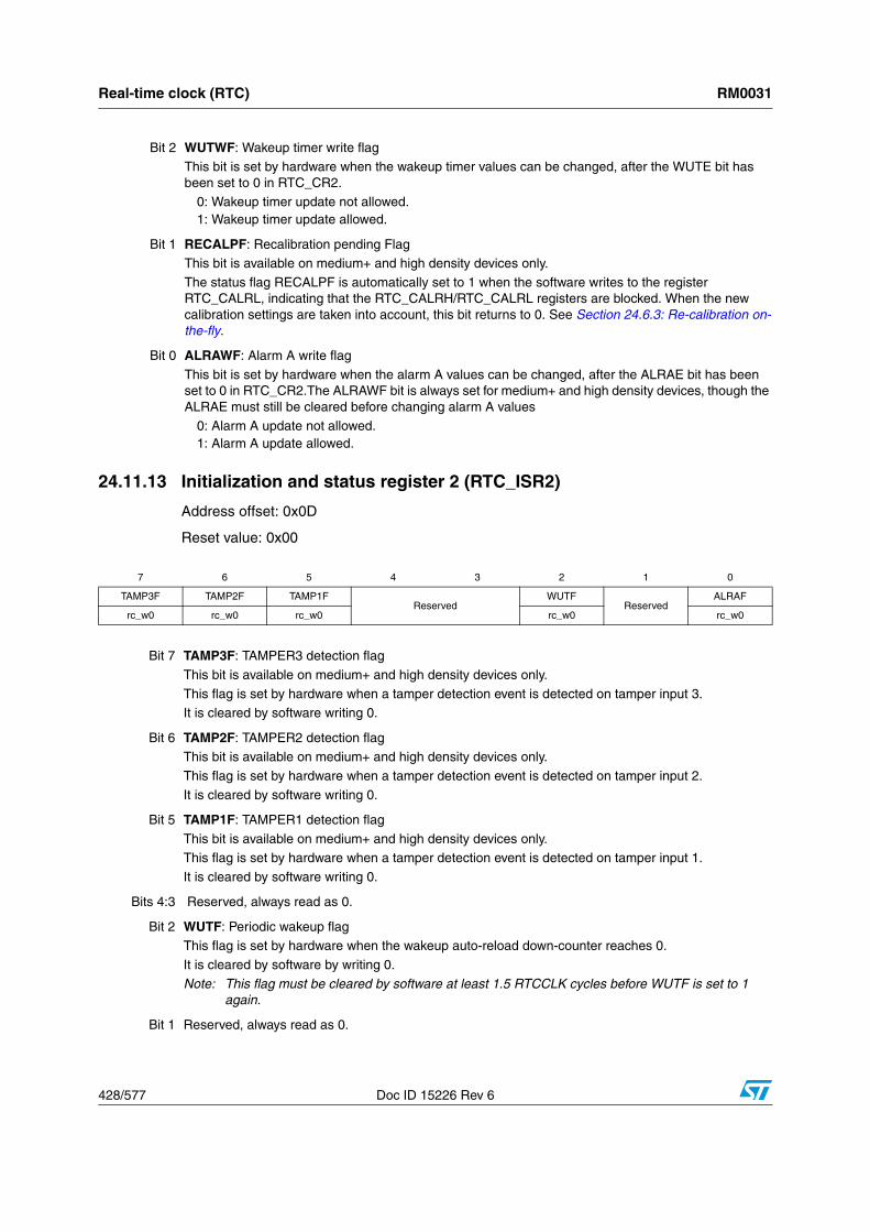
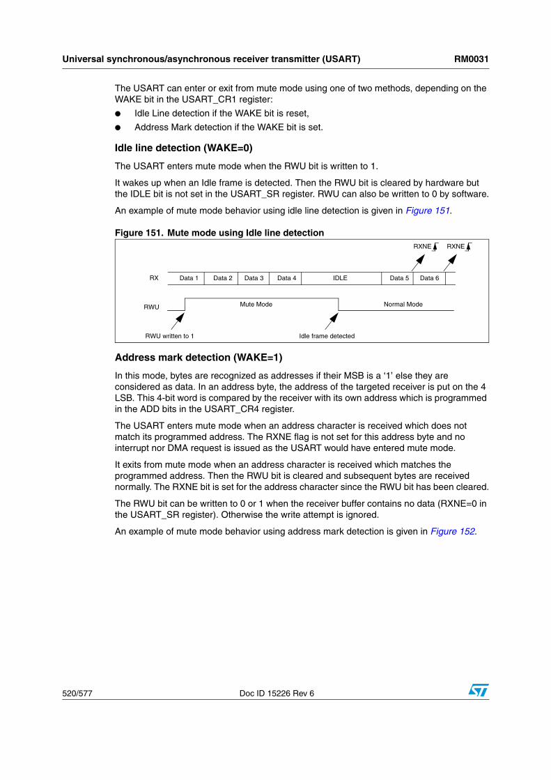
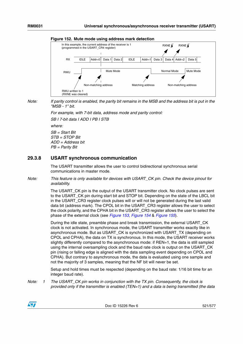
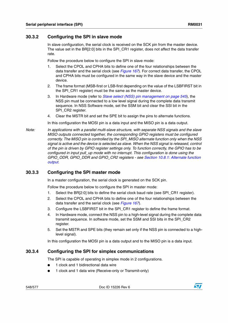
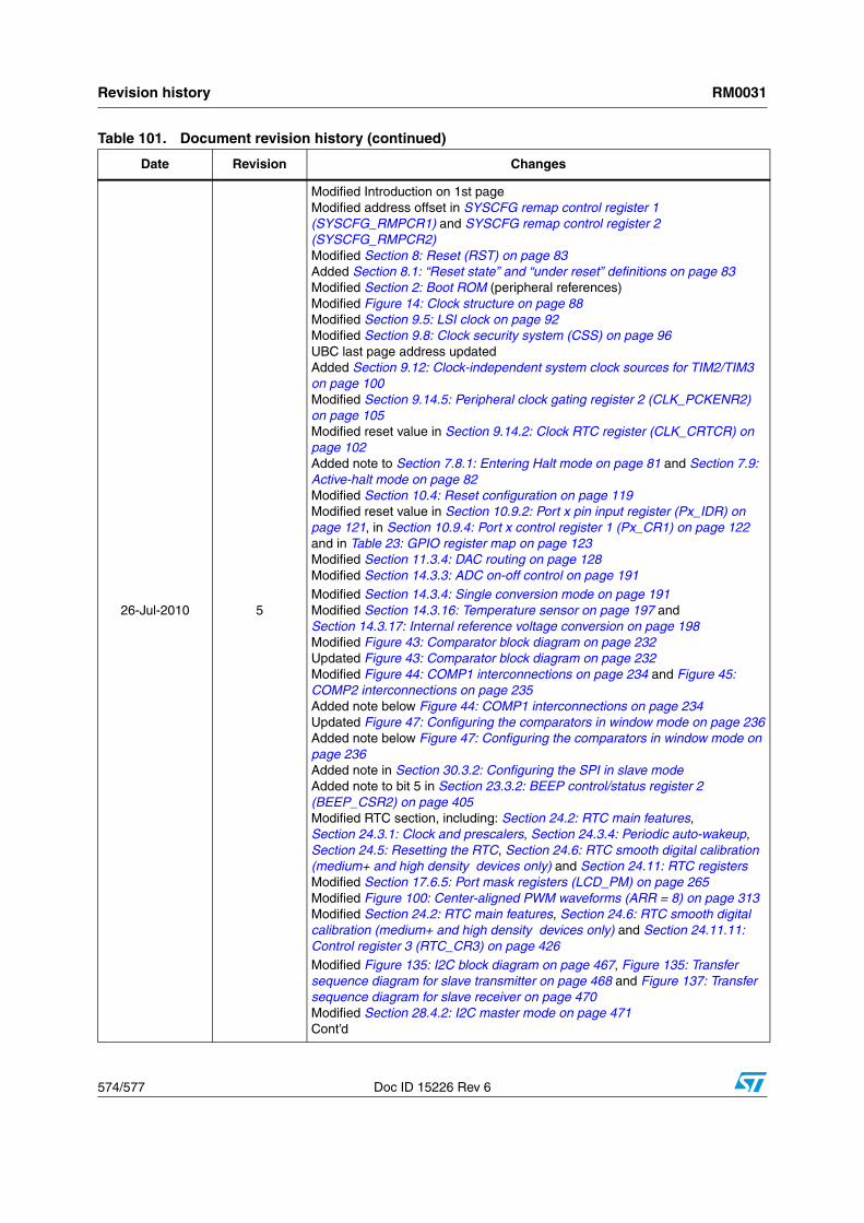
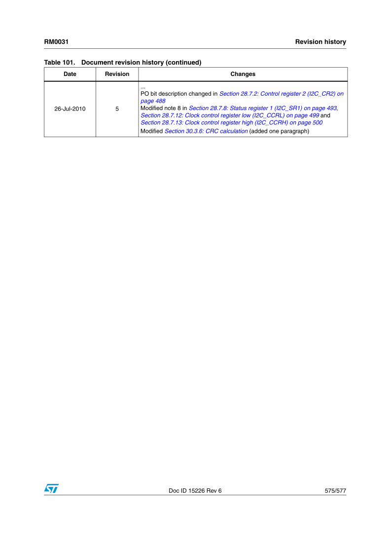
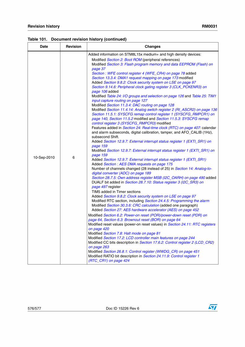
September 2010 Doc ID 15226 Rev 6 1/577 RM0031 Reference manual STM8L15x and STM8L16x microcontroller family Introduction This reference manual targets application developers. It provides complete information on how to use the STM8L15x and STM8L16x microcontroller memory and peripherals. The STM8L15x/STM8L16x is a family of microcontrollers with different memory densities, packages and peripherals. ■ The medium density STM8L15x devices are the STM8L151Cx/Kx/Gx, STM8L152Cx/Kx microcontrollers with a 16-Kbyte or 32-Kbyte Flash memory density. Refer to the product datasheet for the complete list of available peripherals. ■ The medium+ density STM8L15x devices are the STM8L151R6 and STM8L152R6 microcontrollers with a 32-Kbyte Flash memory density. They offer a wider range of peripherals than the medium density devices. Refer to the product datasheet for the complete list of available peripherals. ■ The high density STM8L15x devices are the STM8L151x8 and STM8L152x8 microcontrollers with a Flash memory density equal to 64 Kbytes. They offer the same peripheral set as medium+ density devices. Refer to the product datasheet for the complete list of available peripherals. ■ The high density STM8L16x devices are the STM8L162x8 microcontrollers where the Flash memory density is equal to 64 Kbytes. They offer the same peripheral set as high density STM8L152 devices plus the AES hardware accelerator. Refer to the product datasheet for the complete list of available peripherals. They are designed for ultralow power applications. For ordering information, pin description, mechanical and electrical device characteristics, please refer to the product datasheet. For information on the STM8 SWIM communication protocol and debug module, please refer to the user manual (UM0470). For information on the STM8 core, please refer to the STM8 CPU programming manual (PM0044). For information on programming, erasing and protection of the internal Flash memory please refer to the STM8L Flash programming manual (PM0054). www.st.com
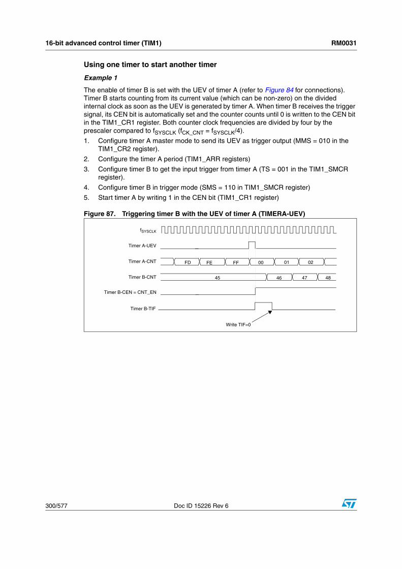
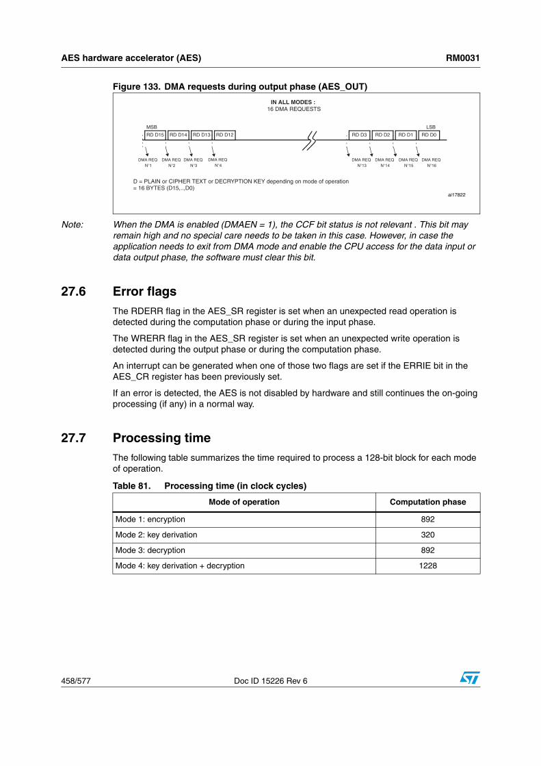
Transcript
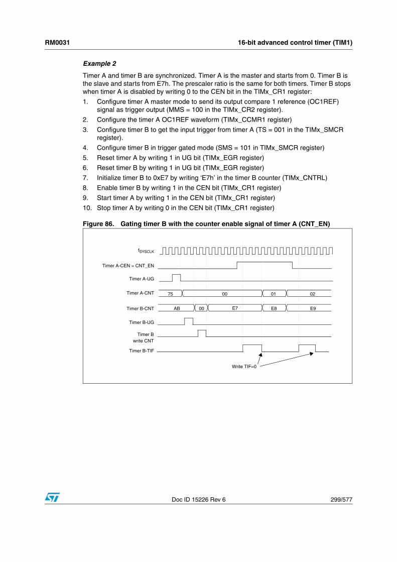
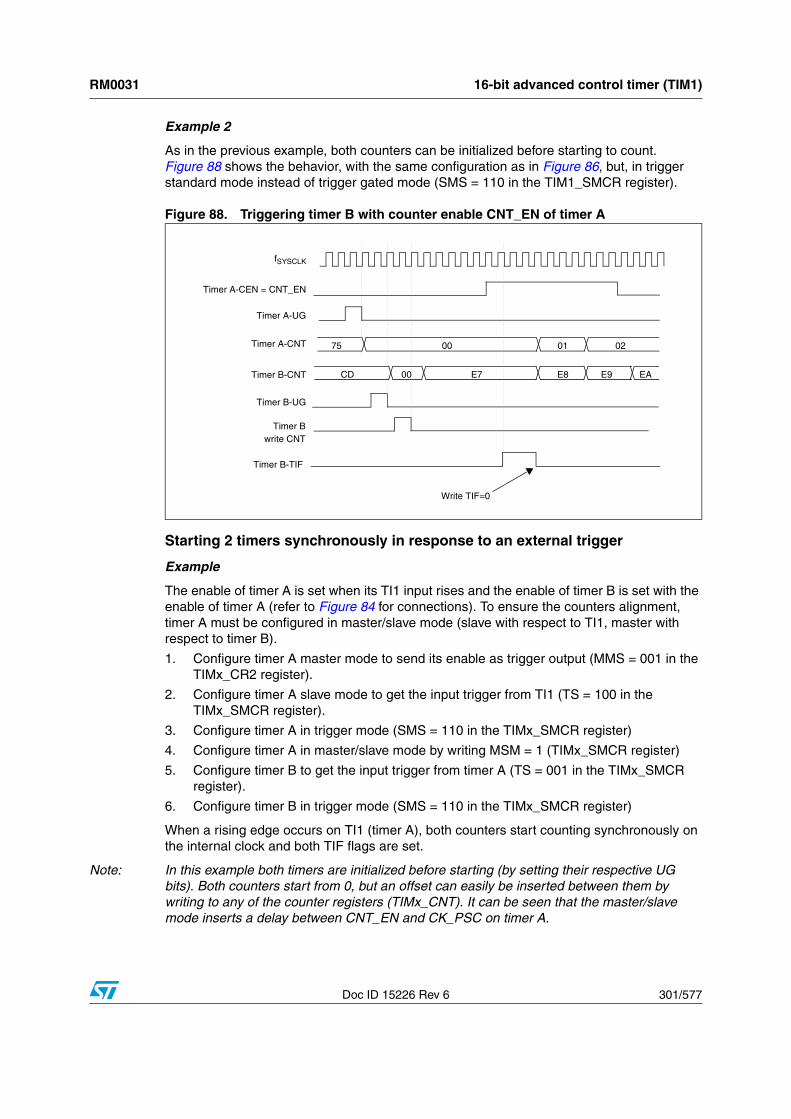
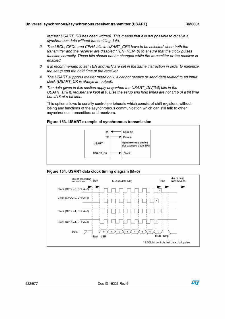
September 2010 Doc ID 15226 Rev 6 1/577
RM0031Reference manual
STM8L15x and STM8L16x microcontroller family
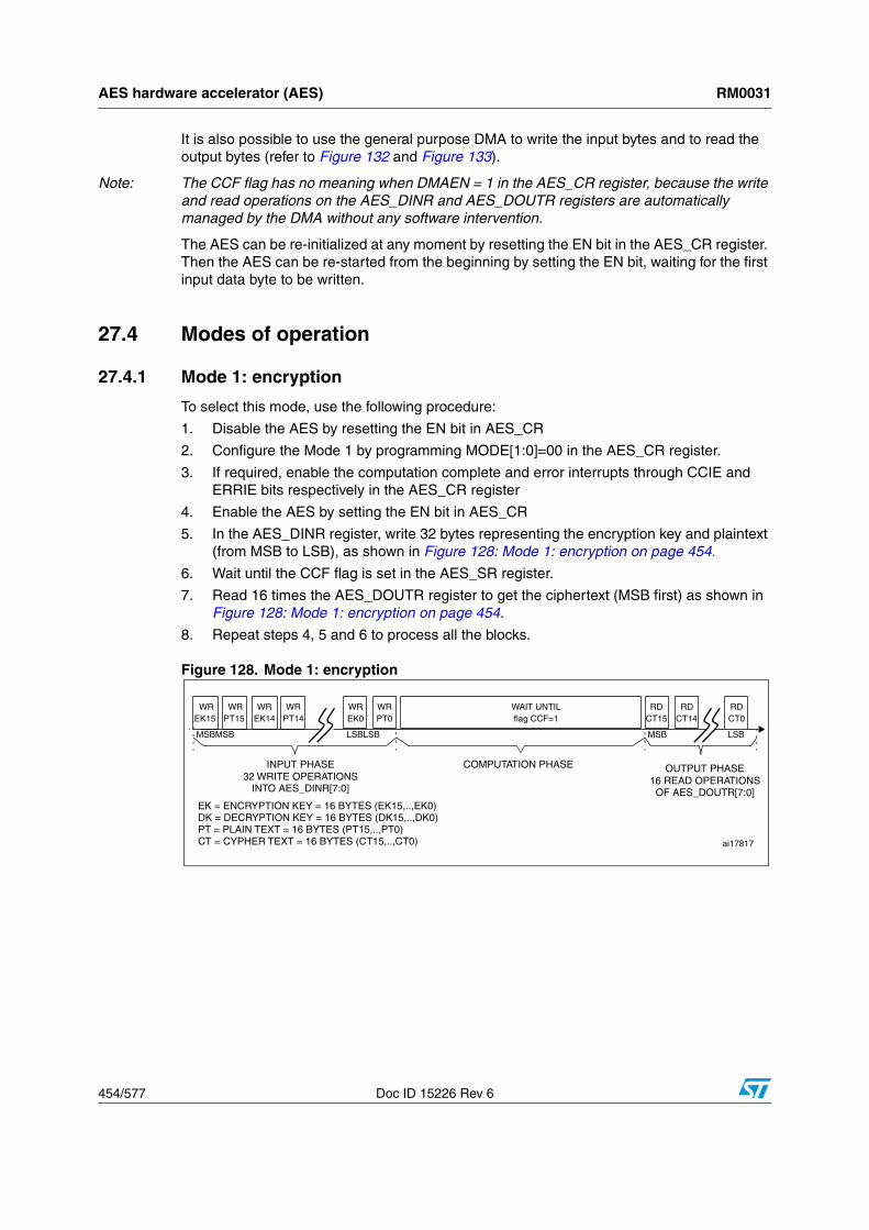
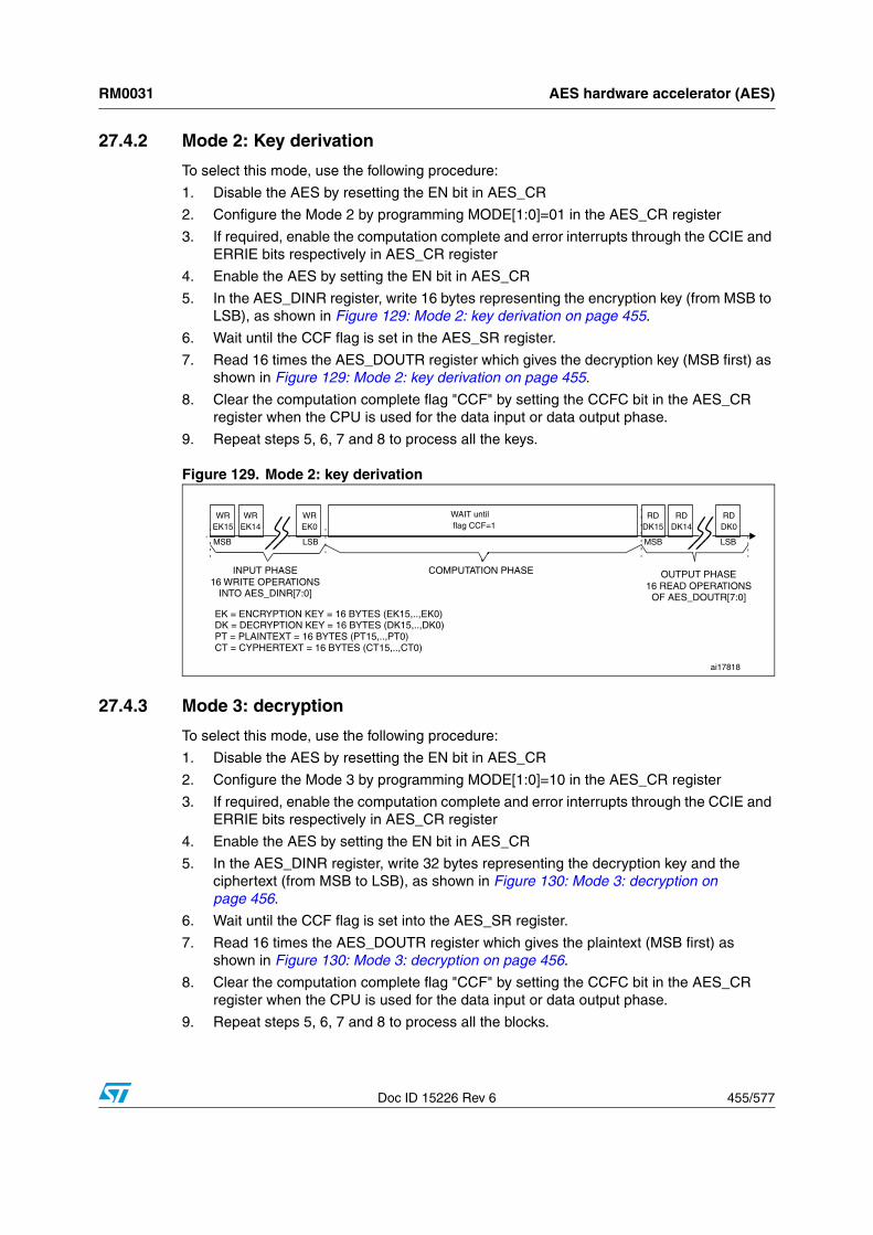
IntroductionThis reference manual targets application developers. It provides complete information on how to use the STM8L15x and STM8L16x microcontroller memory and peripherals.
The STM8L15x/STM8L16x is a family of microcontrollers with different memory densities, packages and peripherals.
■ The medium density STM8L15x devices are the STM8L151Cx/Kx/Gx, STM8L152Cx/Kx microcontrollers with a 16-Kbyte or 32-Kbyte Flash memory density. Refer to the product datasheet for the complete list of available peripherals.
■ The medium+ density STM8L15x devices are the STM8L151R6 and STM8L152R6 microcontrollers with a 32-Kbyte Flash memory density. They offer a wider range of peripherals than the medium density devices.Refer to the product datasheet for the complete list of available peripherals.
■ The high density STM8L15x devices are the STM8L151x8 and STM8L152x8 microcontrollers with a Flash memory density equal to 64 Kbytes. They offer the same peripheral set as medium+ density devices.Refer to the product datasheet for the complete list of available peripherals.
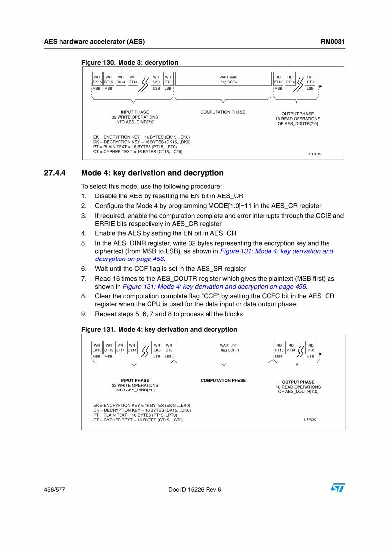
■ The high density STM8L16x devices are the STM8L162x8 microcontrollers where the Flash memory density is equal to 64 Kbytes. They offer the same peripheral set as high density STM8L152 devices plus the AES hardware accelerator.Refer to the product datasheet for the complete list of available peripherals.
They are designed for ultralow power applications.
For ordering information, pin description, mechanical and electrical device characteristics,please refer to the product datasheet.
For information on the STM8 SWIM communication protocol and debug module, please referto the user manual (UM0470).
For information on the STM8 core, please refer to the STM8 CPU programming manual(PM0044).
For information on programming, erasing and protection of the internal Flash memory please refer to the STM8L Flash programming manual (PM0054).
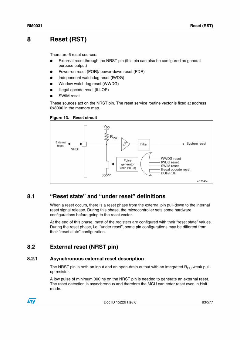
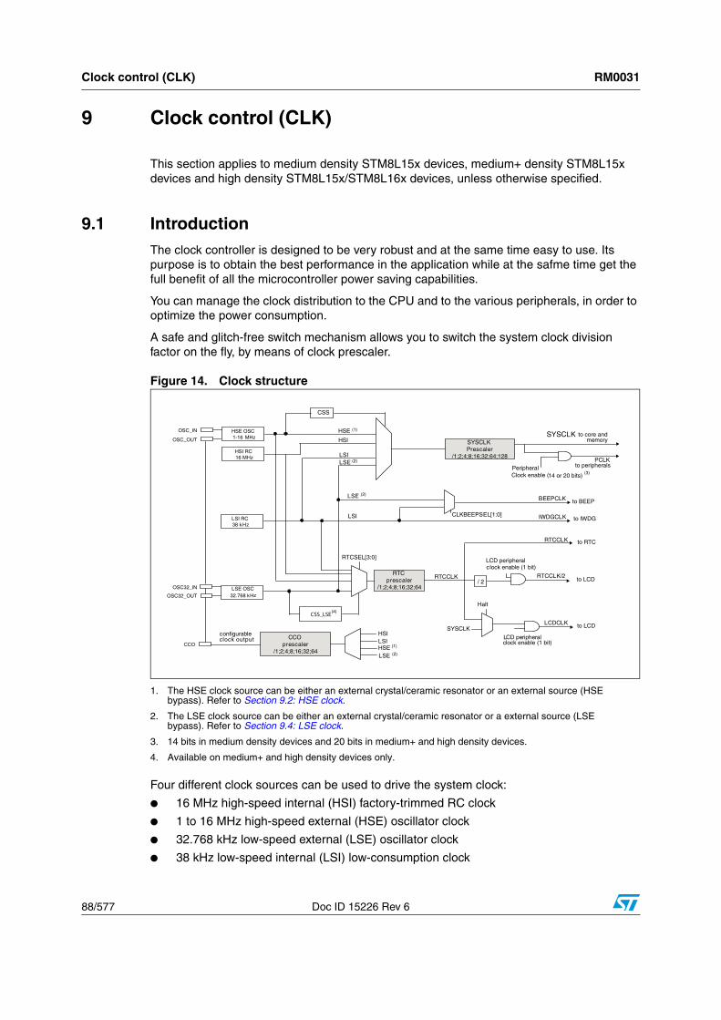
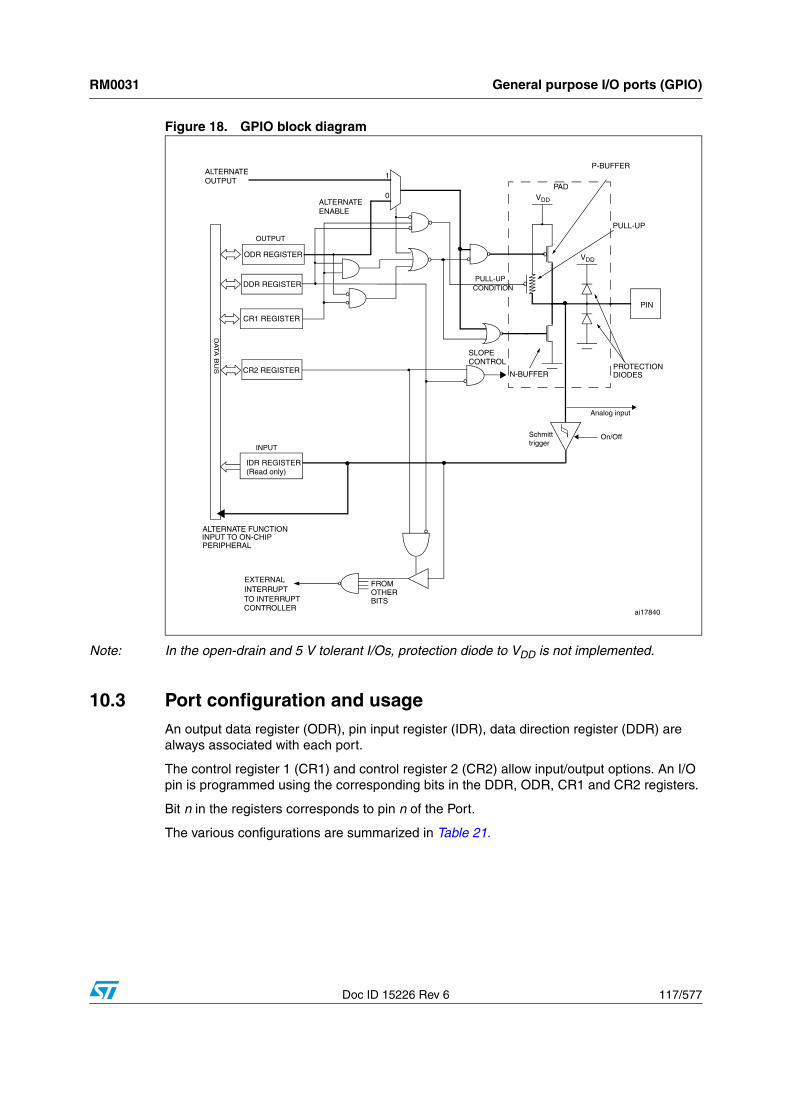
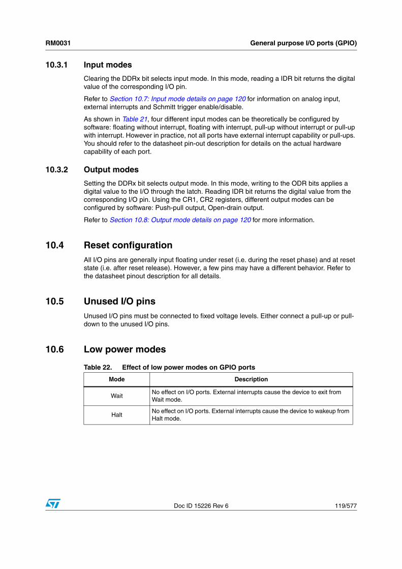
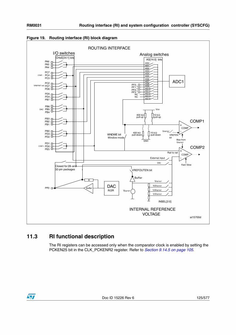
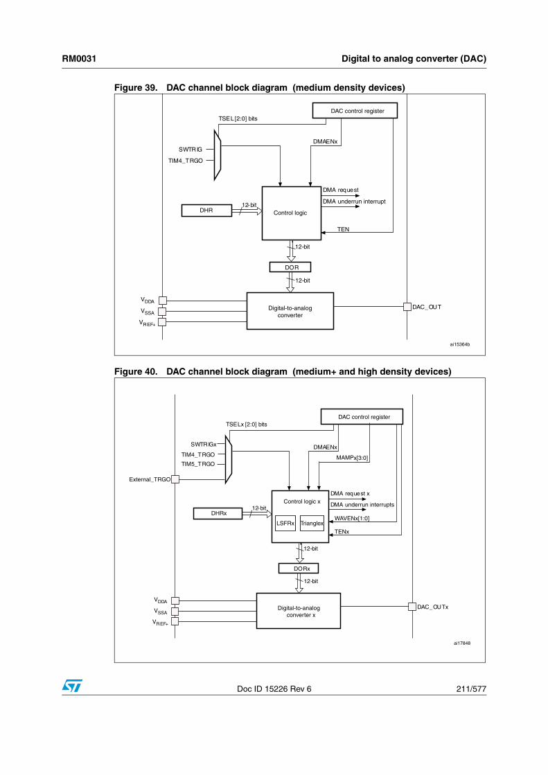
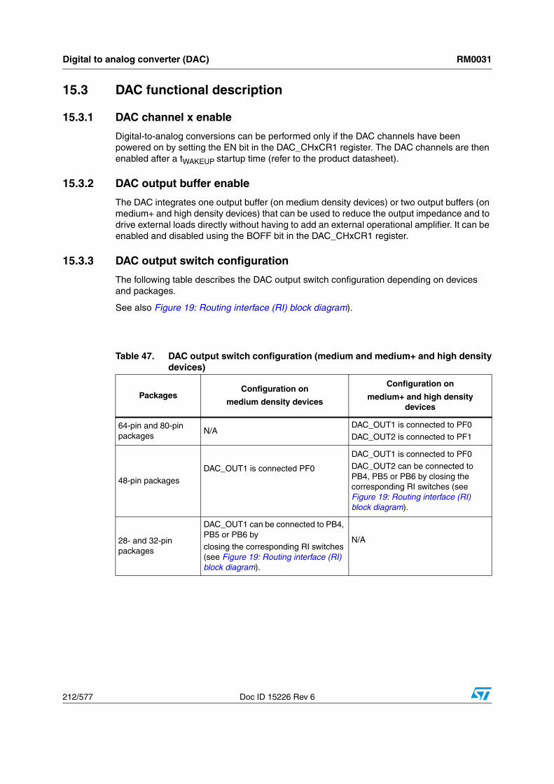
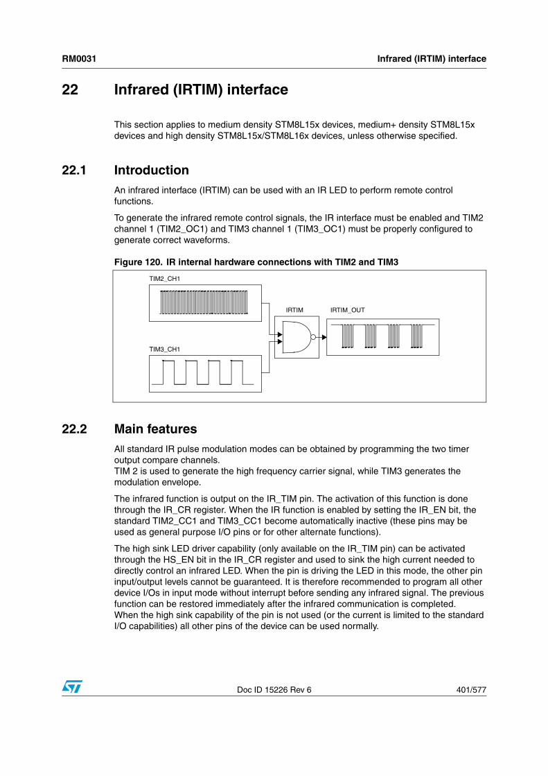
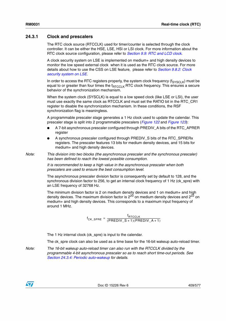
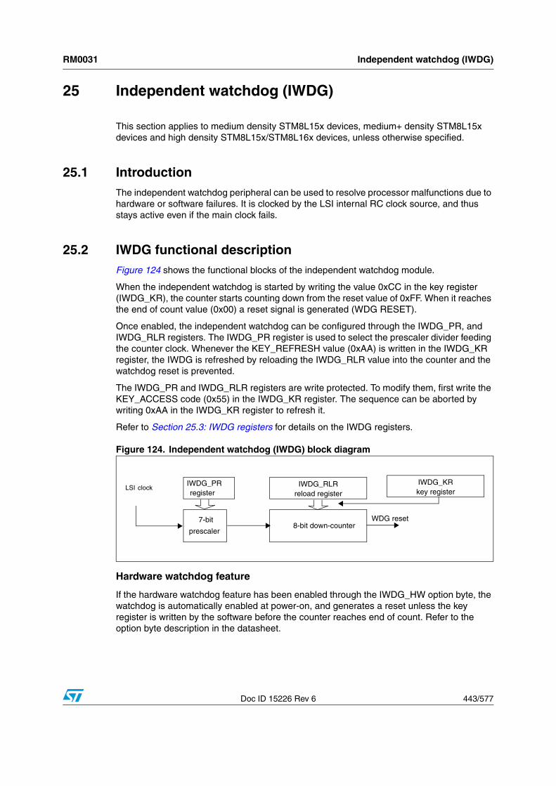
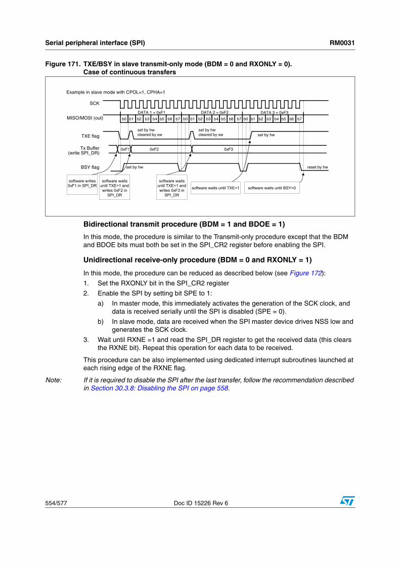
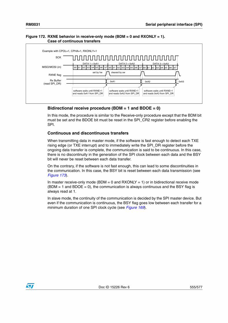
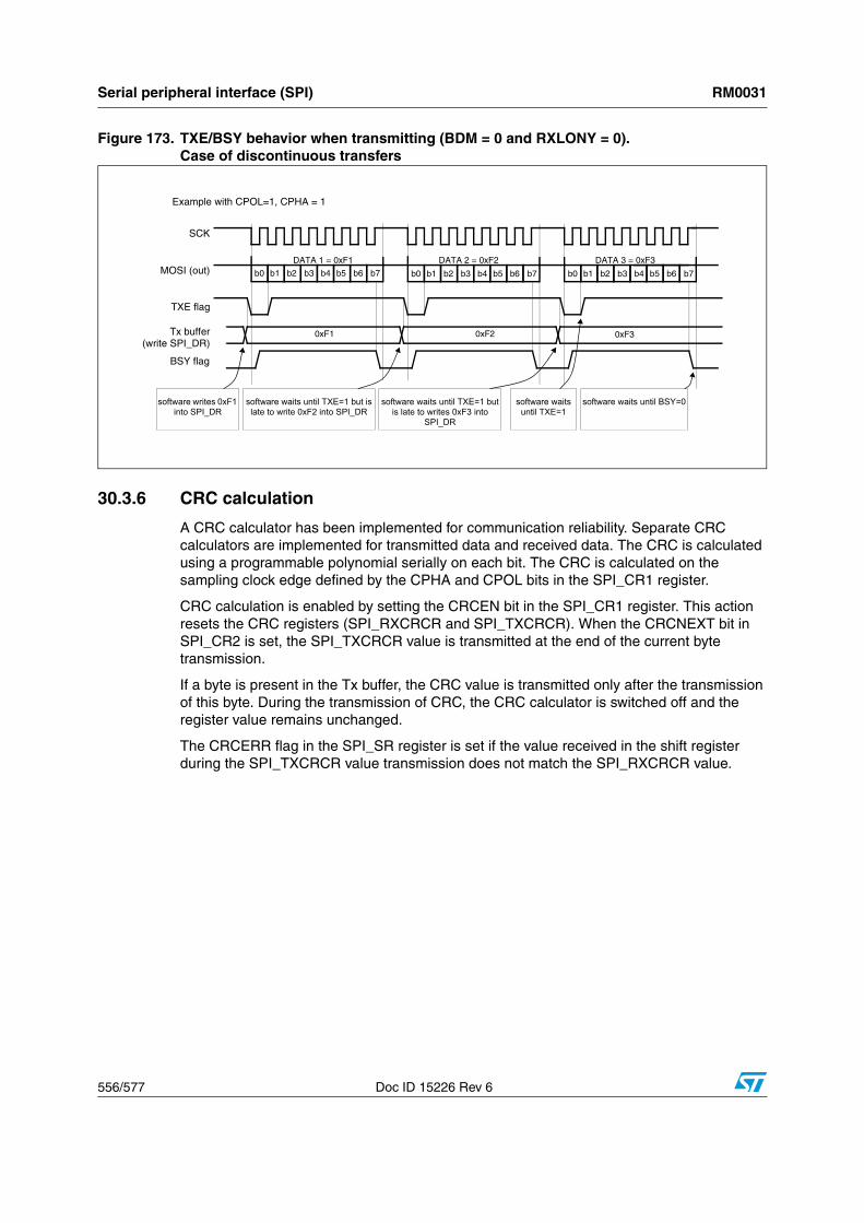
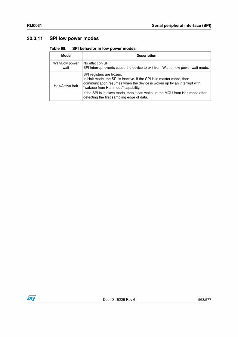
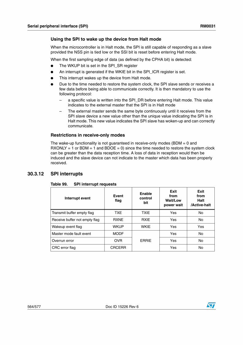
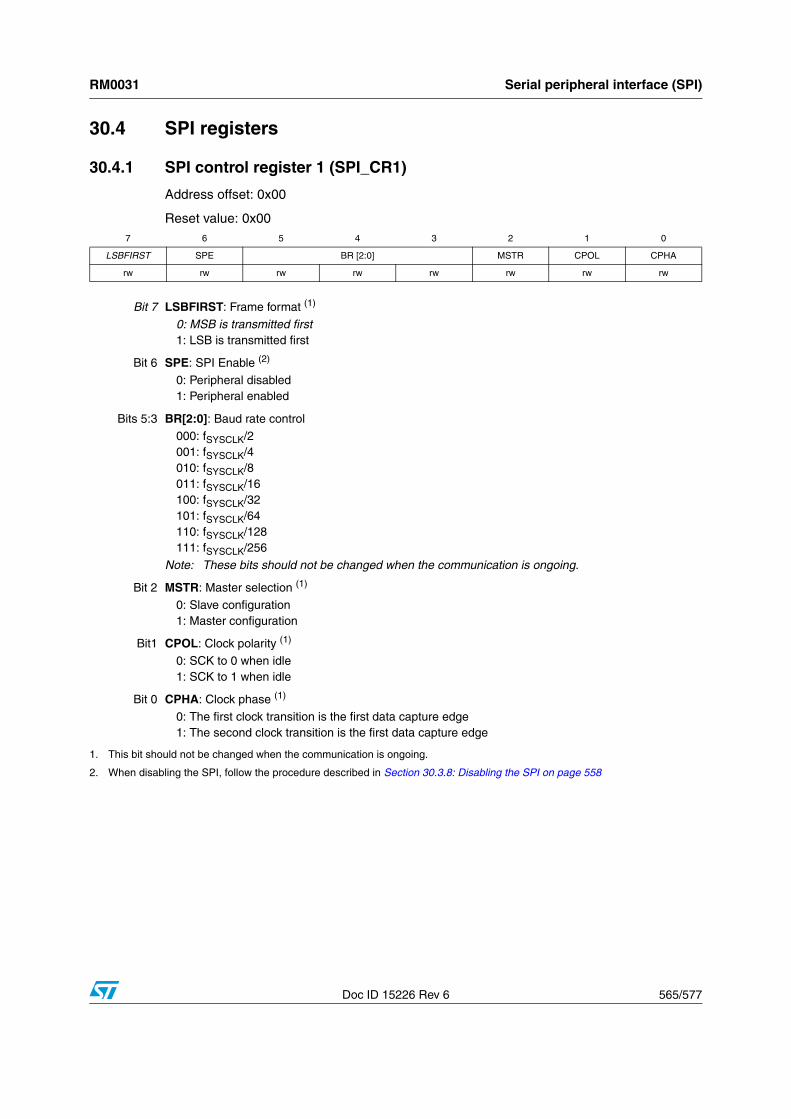
This section applies to medium density STM8L15x devices, medium+ density STM8L15x devices and high density STM8L15x/STM8L16x devices, unless otherwise specified.
1.1 Introduction The CPU has an 8-bit architecture. Six internal registers allow efficient data manipulations. The CPU is able to execute 80 basic instructions. It features 20 addressing modes and can address six internal registers. For the complete description of the instruction set, refer to the STM8 microcontroller family programming manual (PM0044).
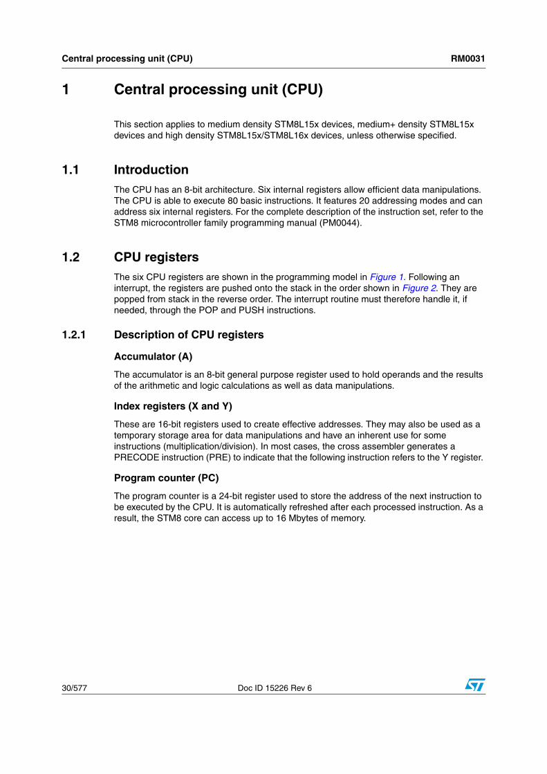
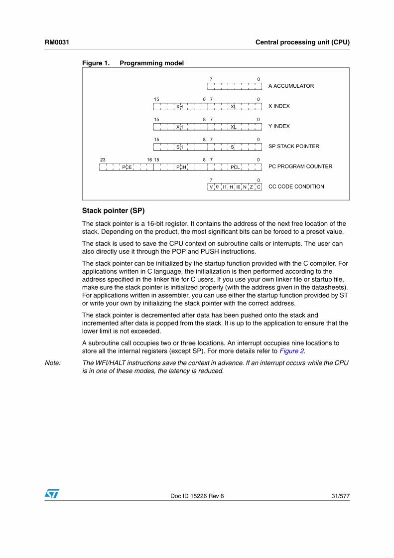
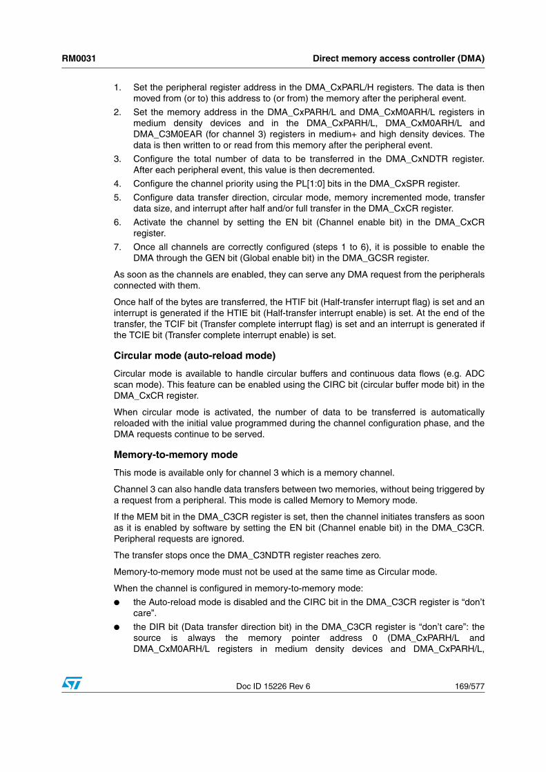
1.2 CPU registers The six CPU registers are shown in the programming model in Figure 1. Following an interrupt, the registers are pushed onto the stack in the order shown in Figure 2. They are popped from stack in the reverse order. The interrupt routine must therefore handle it, if needed, through the POP and PUSH instructions.
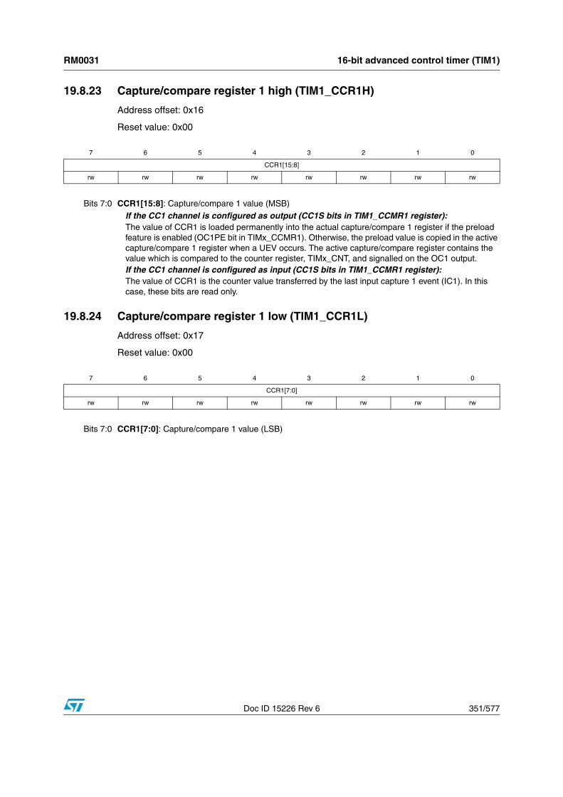
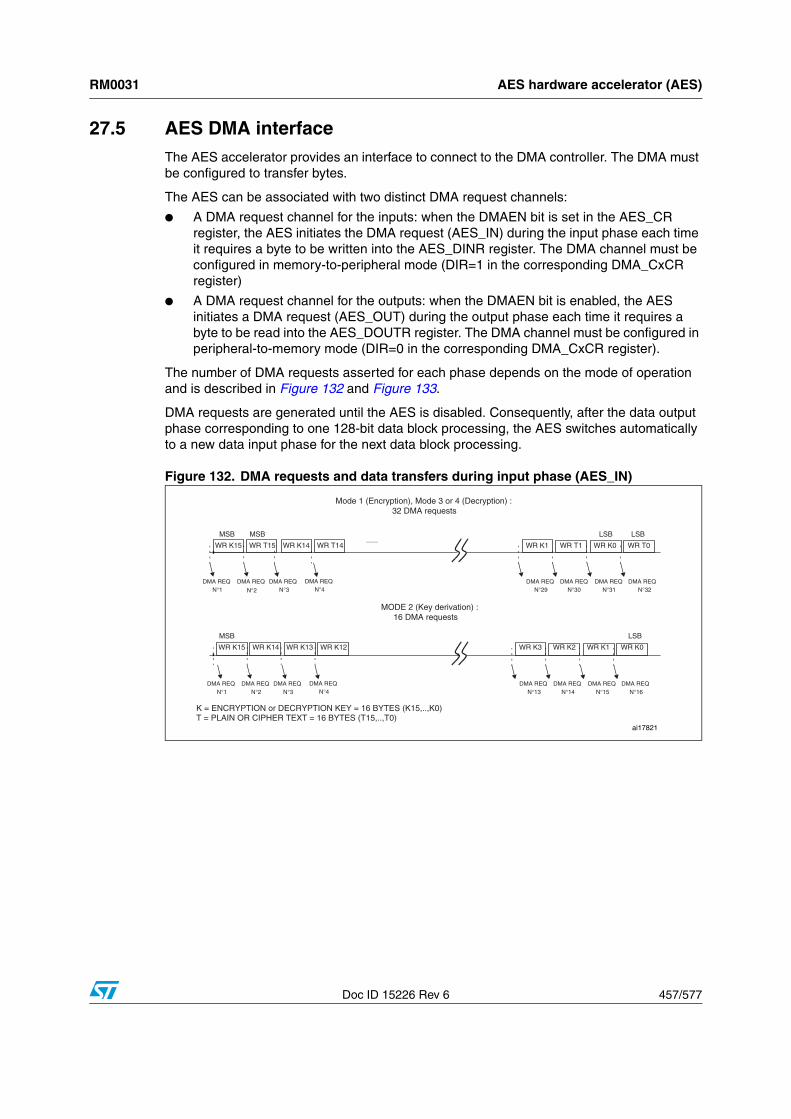
1.2.1 Description of CPU registers
Accumulator (A)
The accumulator is an 8-bit general purpose register used to hold operands and the results of the arithmetic and logic calculations as well as data manipulations.
Index registers (X and Y)
These are 16-bit registers used to create effective addresses. They may also be used as a temporary storage area for data manipulations and have an inherent use for some instructions (multiplication/division). In most cases, the cross assembler generates a PRECODE instruction (PRE) to indicate that the following instruction refers to the Y register.
Program counter (PC)
The program counter is a 24-bit register used to store the address of the next instruction to be executed by the CPU. It is automatically refreshed after each processed instruction. As a result, the STM8 core can access up to 16 Mbytes of memory.
RM0031 Central processing unit (CPU)
Doc ID 15226 Rev 6 31/577
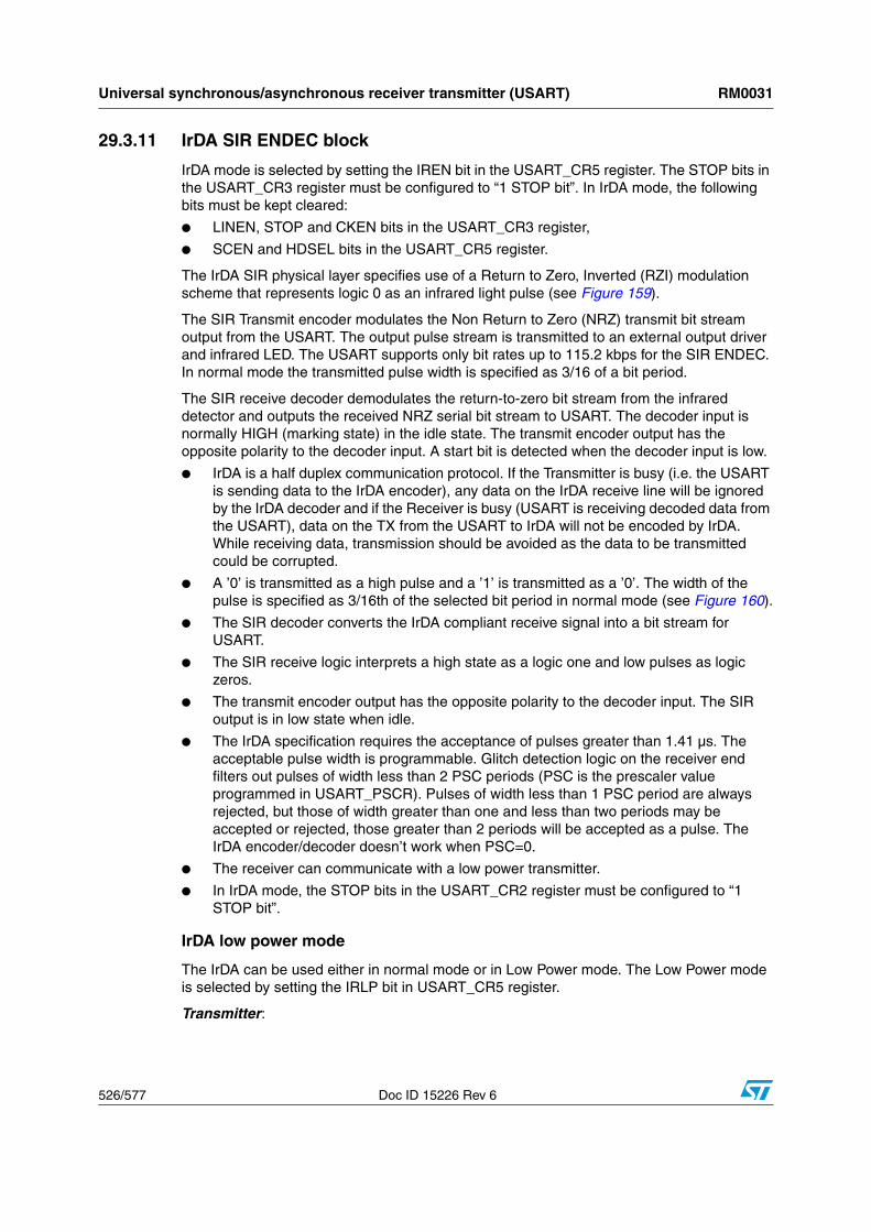
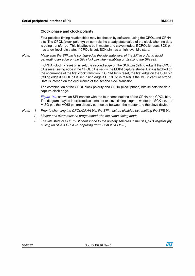
Figure 1. Programming model
Stack pointer (SP)
The stack pointer is a 16-bit register. It contains the address of the next free location of the stack. Depending on the product, the most significant bits can be forced to a preset value.
The stack is used to save the CPU context on subroutine calls or interrupts. The user can also directly use it through the POP and PUSH instructions.
The stack pointer can be initialized by the startup function provided with the C compiler. For applications written in C language, the initialization is then performed according to the address specified in the linker file for C users. If you use your own linker file or startup file, make sure the stack pointer is initialized properly (with the address given in the datasheets). For applications written in assembler, you can use either the startup function provided by ST or write your own by initializing the stack pointer with the correct address.
The stack pointer is decremented after data has been pushed onto the stack and incremented after data is popped from the stack. It is up to the application to ensure that the lower limit is not exceeded.
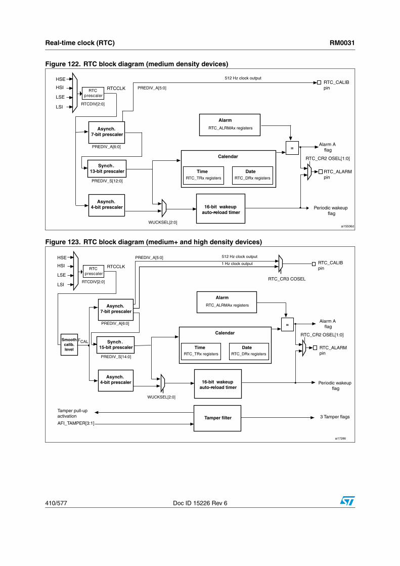
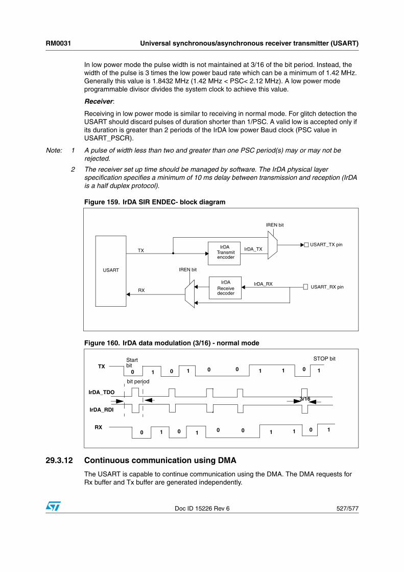
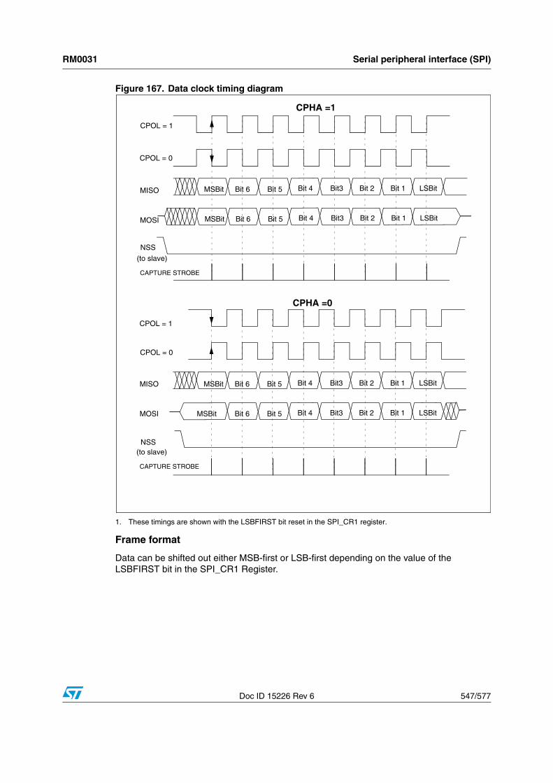
A subroutine call occupies two or three locations. An interrupt occupies nine locations to store all the internal registers (except SP). For more details refer to Figure 2.
Note: The WFI/HALT instructions save the context in advance. If an interrupt occurs while the CPU is in one of these modes, the latency is reduced.
07A ACCUMULATOR
07815SP STACK POINTERSH S
X INDEX
Y INDEX
07815PC PROGRAM COUNTERPCH PCL
07CC CODE CONDITIONV I1 H I0 N Z C
1623PCE
07815XH XL
07815XH XL
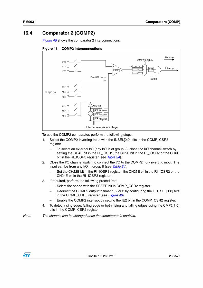
0
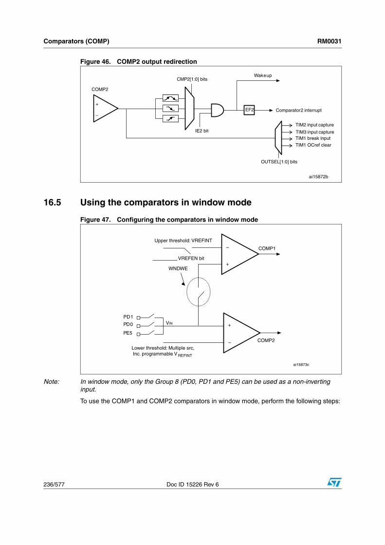
Central processing unit (CPU) RM0031
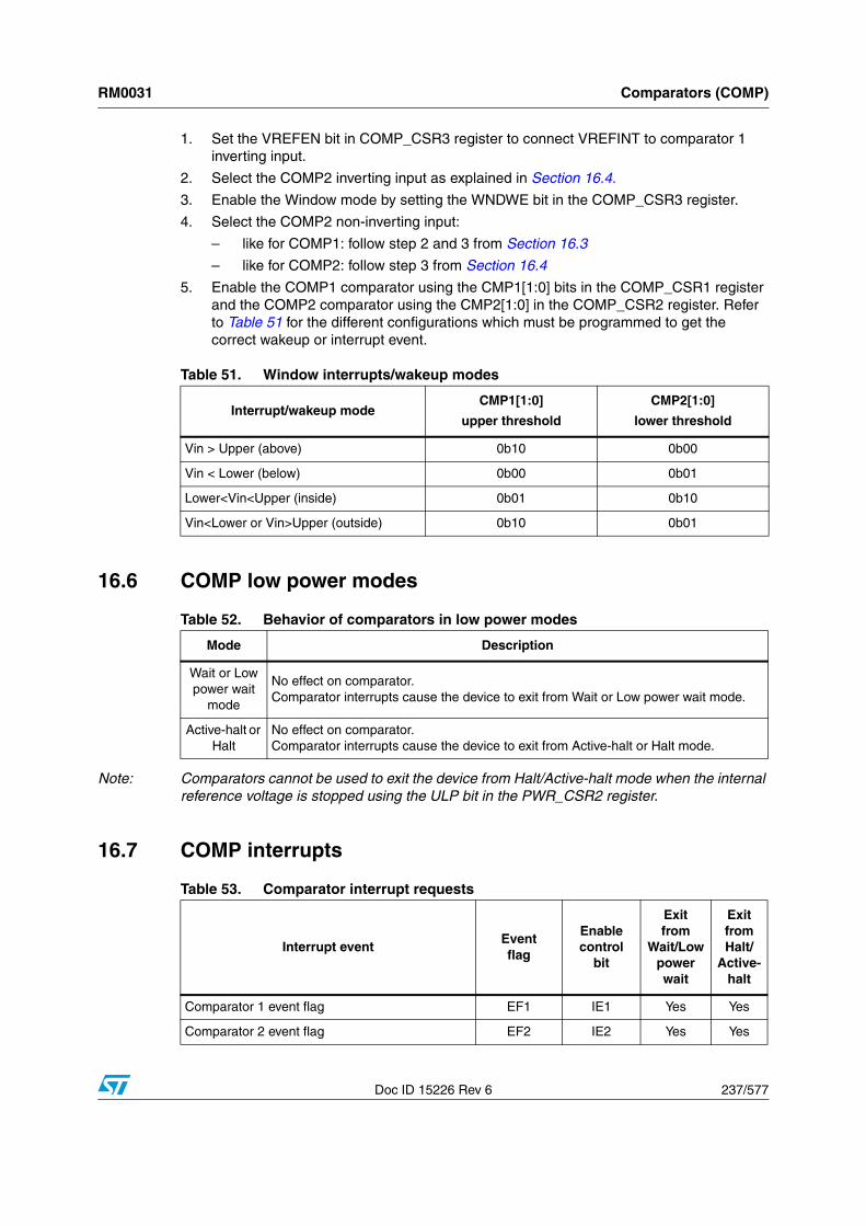
32/577 Doc ID 15226 Rev 6
Figure 2. Stacking order
Condition code register (CC)
The condition code register is an 8-bit register which indicates the result of the instruction just executed as well as the state of the processor. The 7th bit (MSB) of this register is reserved. These bits can be individually tested by a program and specified action taken as a result of their state. The following paragraphs describe each bit:
● V: Overflow
When set, V indicates that an overflow occurred during the last signed arithmetic operation, on the MSB result bit. See the INC, INCW, DEC, DECW, NEG, NEGW, ADD, ADDW, ADC, SUB, SUBW, SBC, CP, and CPW instructions.
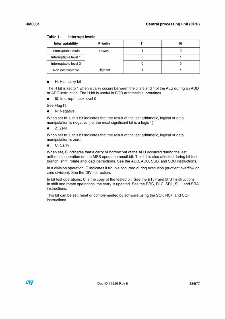
● I1: Interrupt mask level 1
The I1 flag works in conjunction with the I0 flag to define the current interruptability level as shown in Table 1. These flags can be set and cleared by software through the RIM, SIM, HALT, WFI, WFE, IRET, TRAP, and POP instructions and are automatically set by hardware when entering an interrupt service routine.
JUMP TO INTERRUPT ROUTINE GIVEN BY THE INTERRUPT VECTOR
INTERRUPT GENERATION (execute pipeline)
YHYL
PCE
PCL
CC
STACK(PUSH)
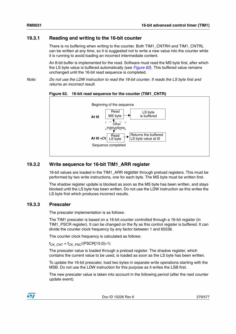
UNSTACK
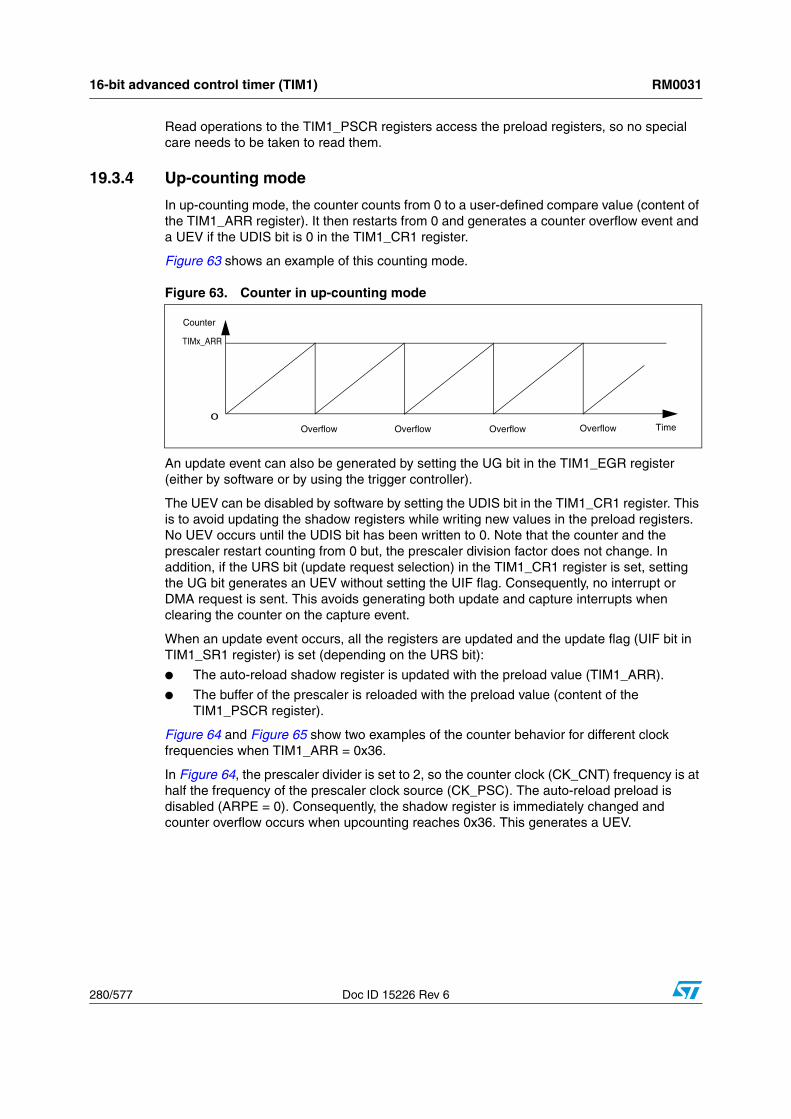
INTER
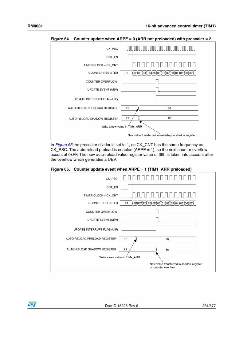
RU
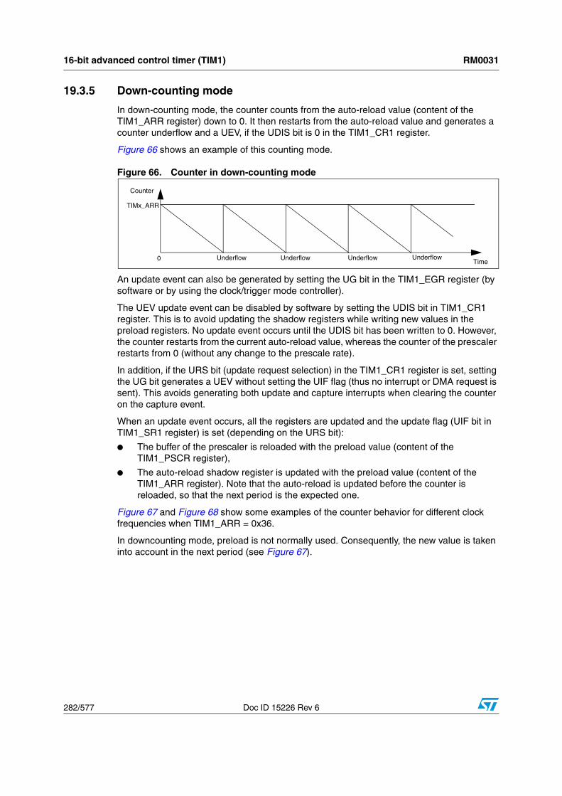
PT
RETU
RN
PCH
JUMP TO THE ADDRESS GIVEN BY PROGRAM COUNTER (Reload Pipeline)
IRET INSTRUCTION
(POP)
9 CPU CYCLES
9 CPU CYCLESPOP PCLPOP PCHPOP PCE
POP YPOP XPOP A
POP CC
AXHXL
PUSH PCLPUSH PCHPUSH PCE
PUSH YPUSH XPUSH A
PUSH CC
Complete instruction in execute stage (1-6 cycles latency)
RM0031 Central processing unit (CPU)
Doc ID 15226 Rev 6 33/577
● H: Half carry bit
The H bit is set to 1 when a carry occurs between the bits 3 and 4 of the ALU during an ADD or ADC instruction. The H bit is useful in BCD arithmetic subroutines.
● I0: Interrupt mask level 0
See Flag I1.
● N: Negative
When set to 1, this bit indicates that the result of the last arithmetic, logical or data manipulation is negative (i.e. the most significant bit is a logic 1).
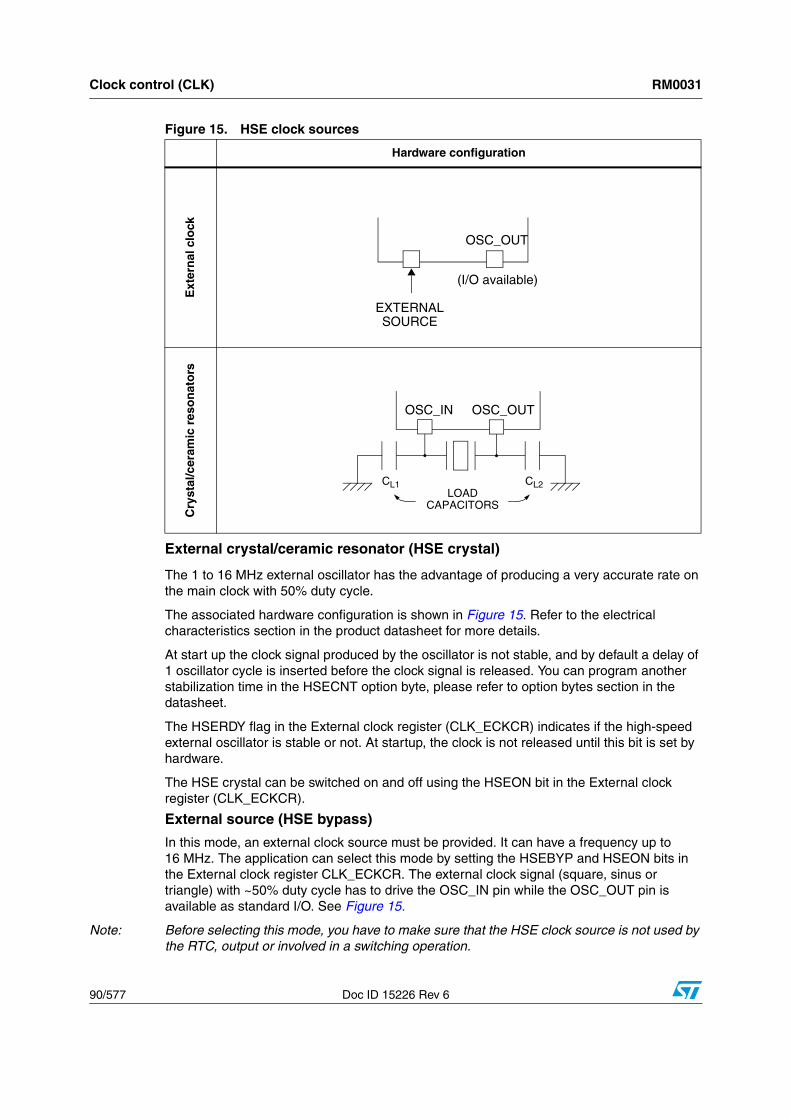
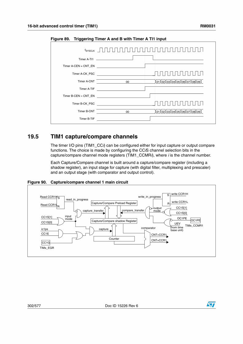
● Z: Zero
When set to 1, this bit indicates that the result of the last arithmetic, logical or data manipulation is zero.
● C: Carry
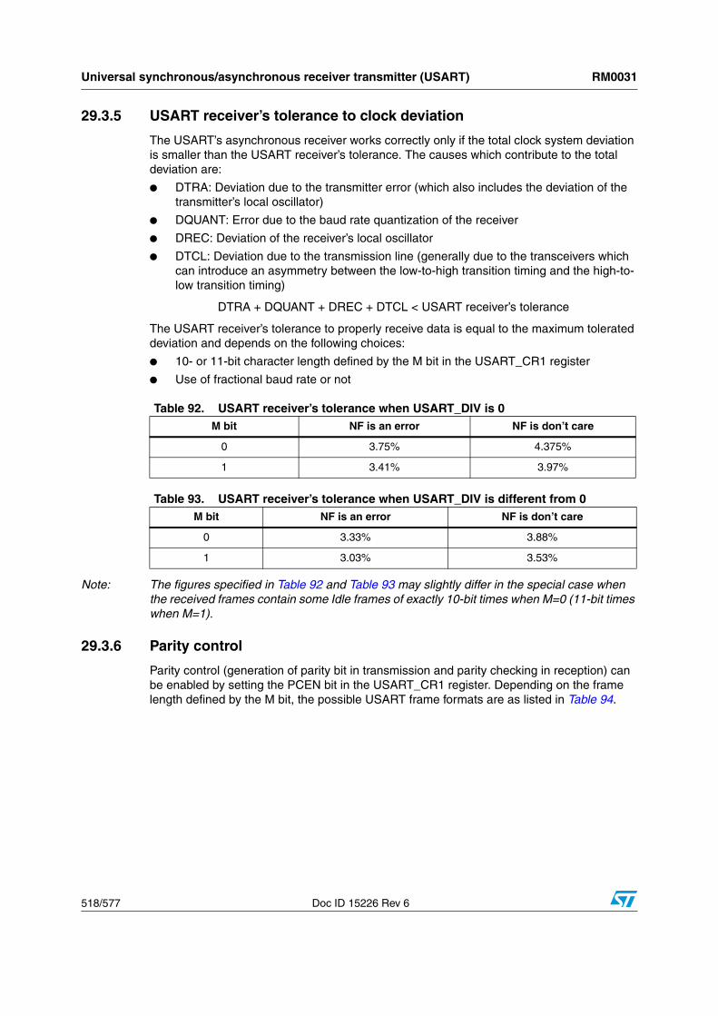
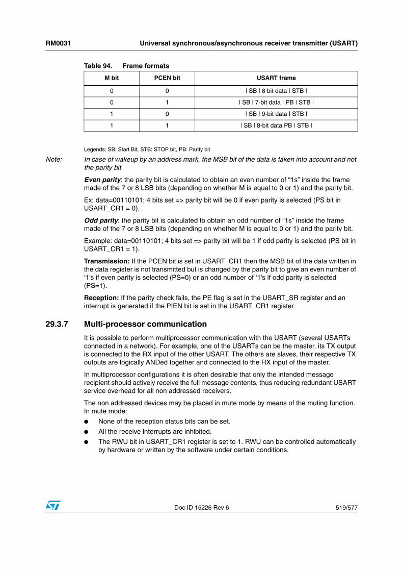
When set, C indicates that a carry or borrow out of the ALU occurred during the last arithmetic operation on the MSB operation result bit. This bit is also affected during bit test, branch, shift, rotate and load instructions. See the ADD, ADC, SUB, and SBC instructions.
In a division operation, C indicates if trouble occurred during execution (quotient overflow or zero division). See the DIV instruction.
In bit test operations, C is the copy of the tested bit. See the BTJF and BTJT instructions.In shift and rotate operations, the carry is updated. See the RRC, RLC, SRL, SLL, and SRA instructions.
This bit can be set, reset or complemented by software using the SCF, RCF, and CCF instructions.
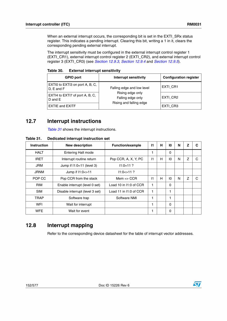
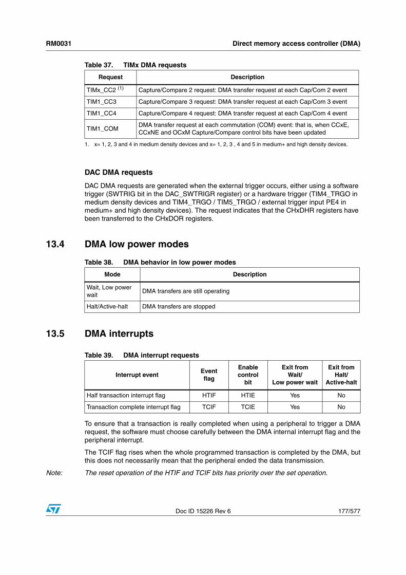
Table 1. Interrupt levels
Interruptability Priority I1 I0
Interruptable main Lowest
Highest
1 0
Interruptable level 1 0 1
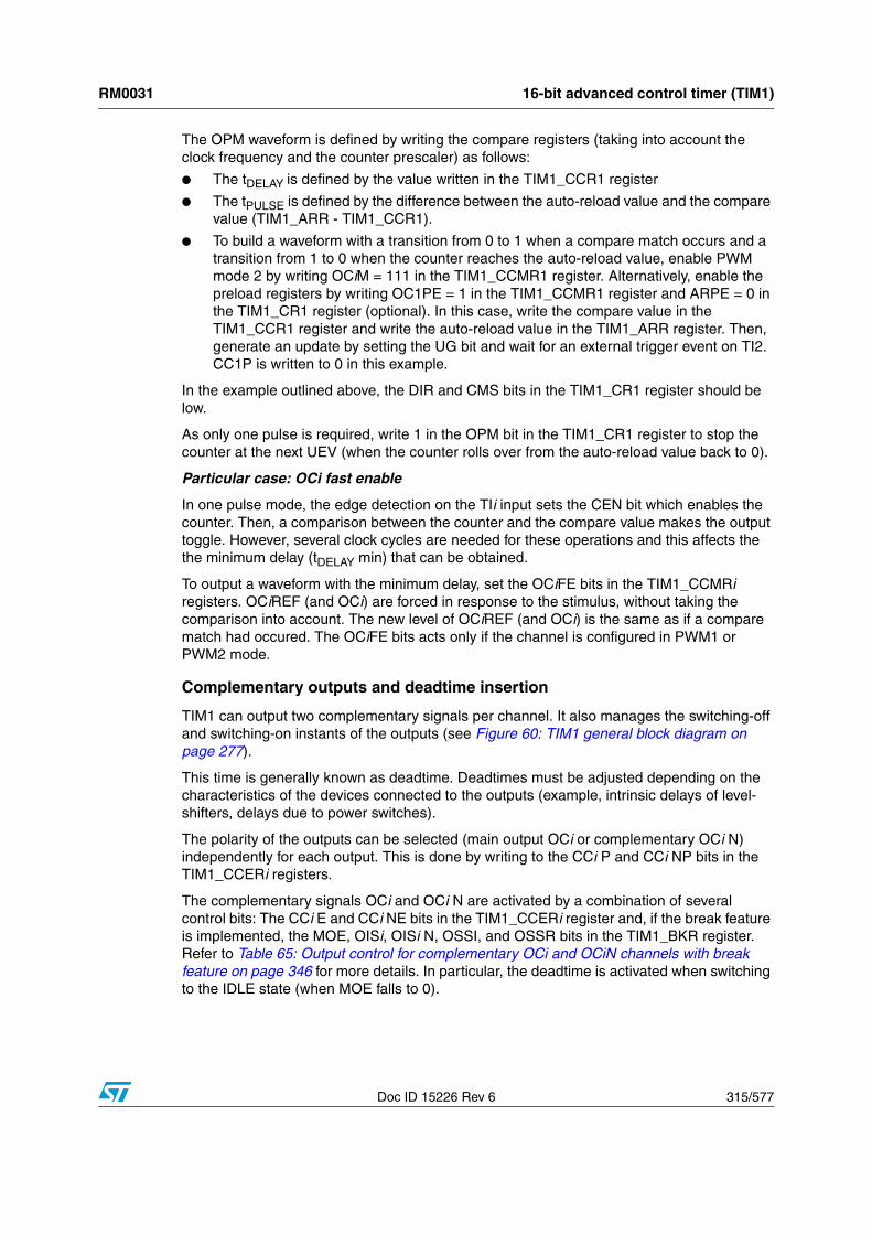
Interruptable level 2 0 0
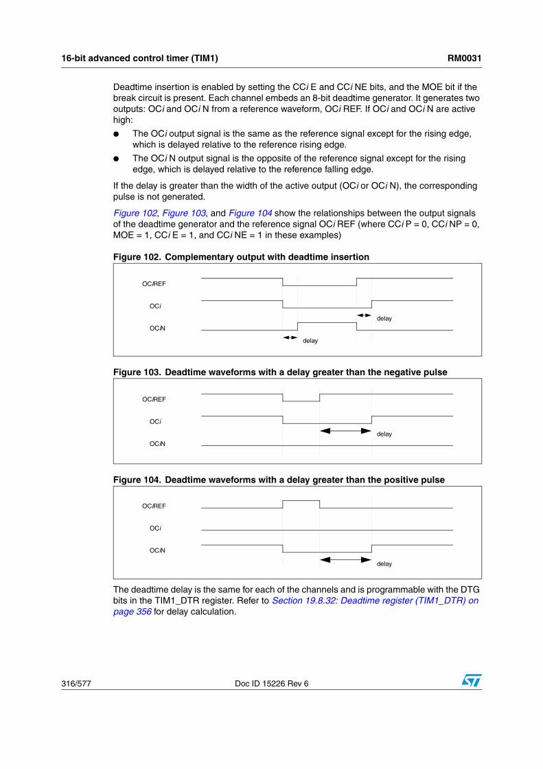
Non interruptable 1 1
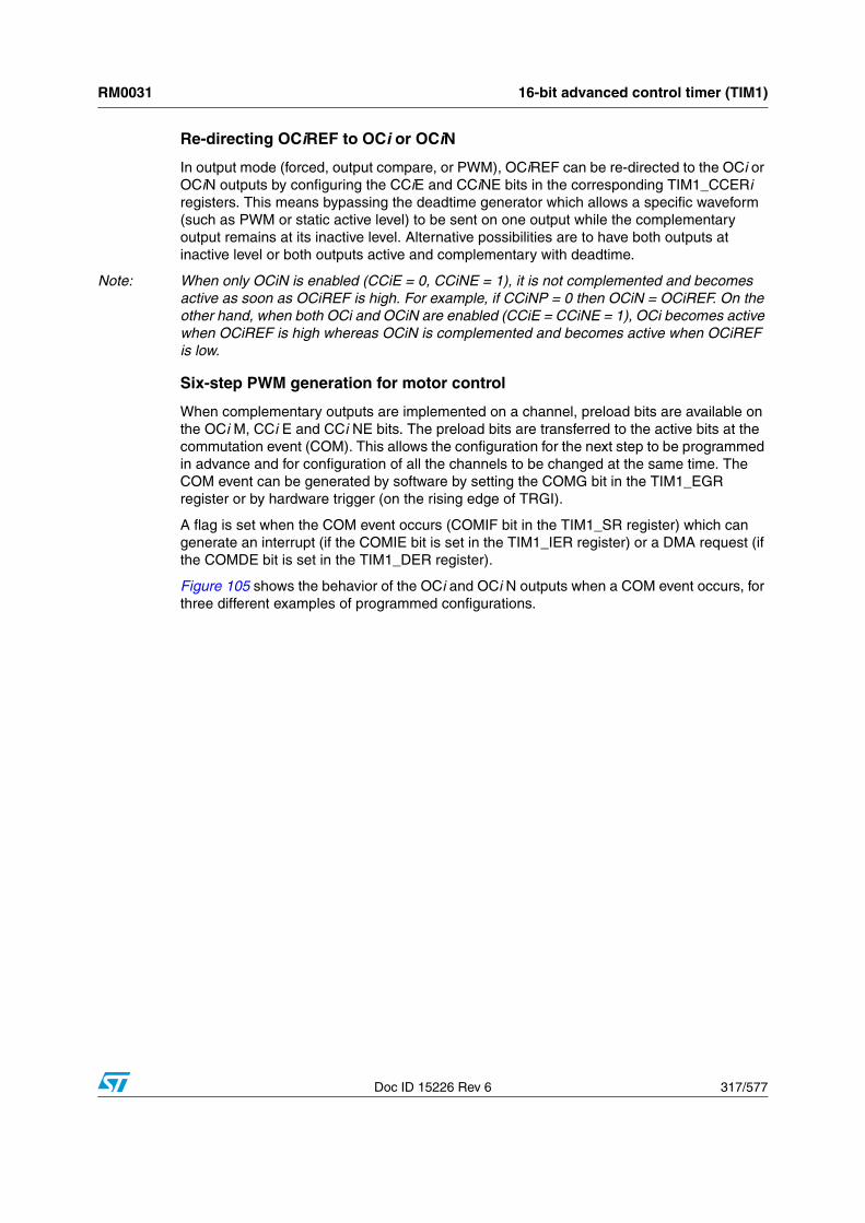
Central processing unit (CPU) RM0031
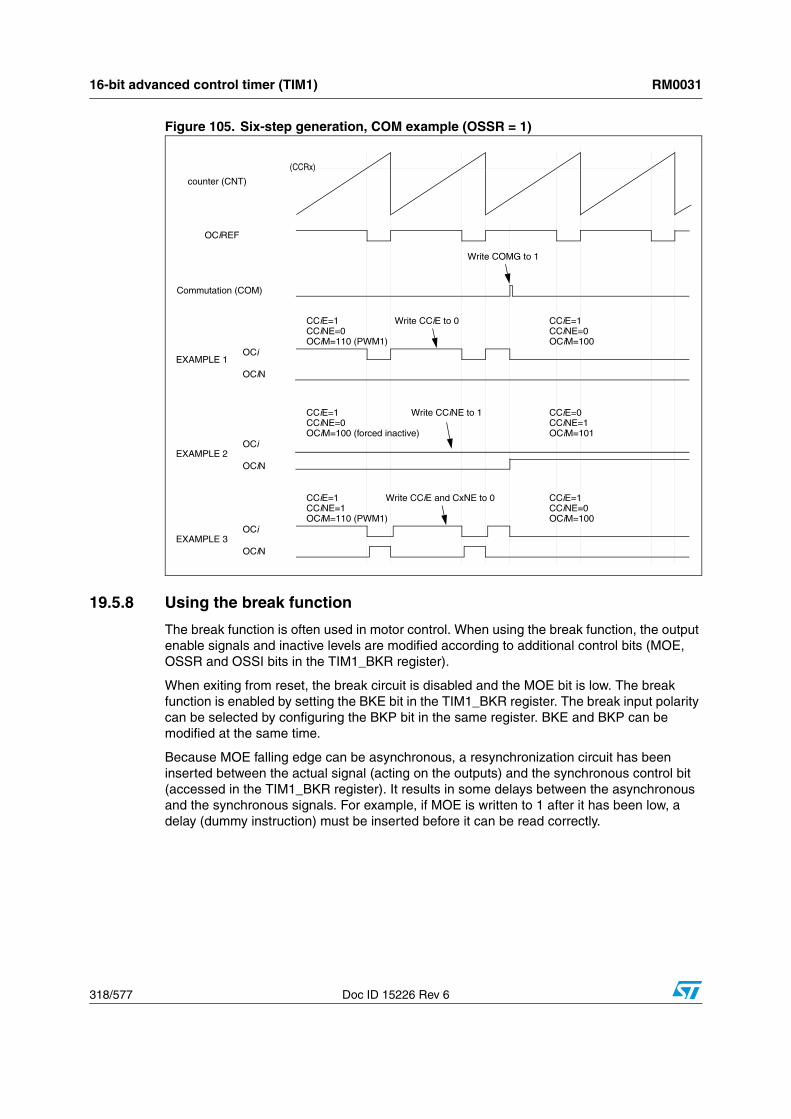
34/577 Doc ID 15226 Rev 6
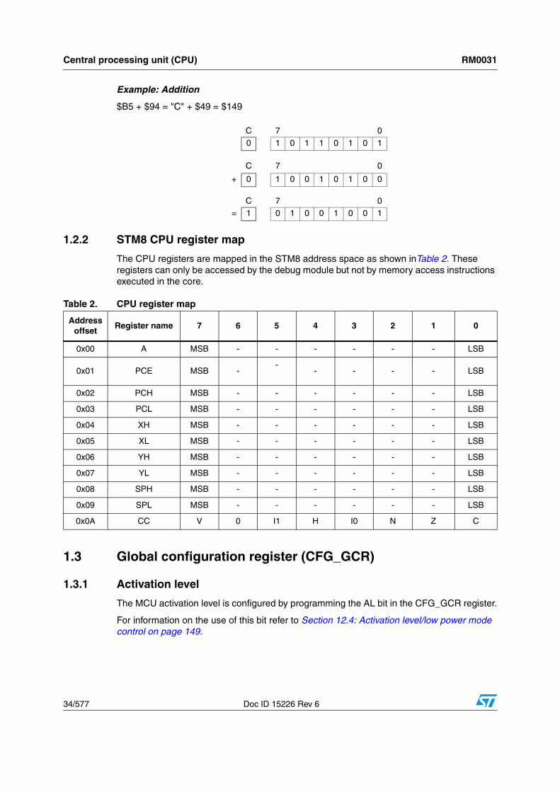
Example: Addition
$B5 + $94 = "C" + $49 = $149
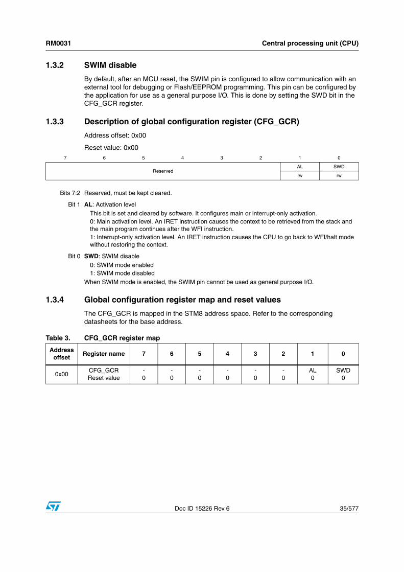
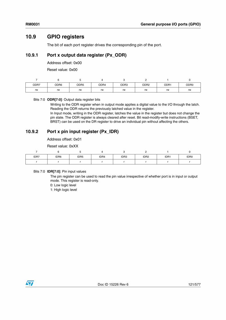
1.2.2 STM8 CPU register map
The CPU registers are mapped in the STM8 address space as shown inTable 2. These registers can only be accessed by the debug module but not by memory access instructions executed in the core.
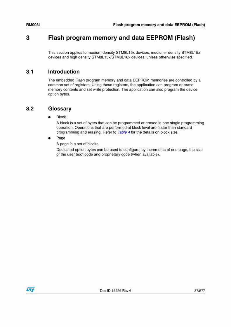
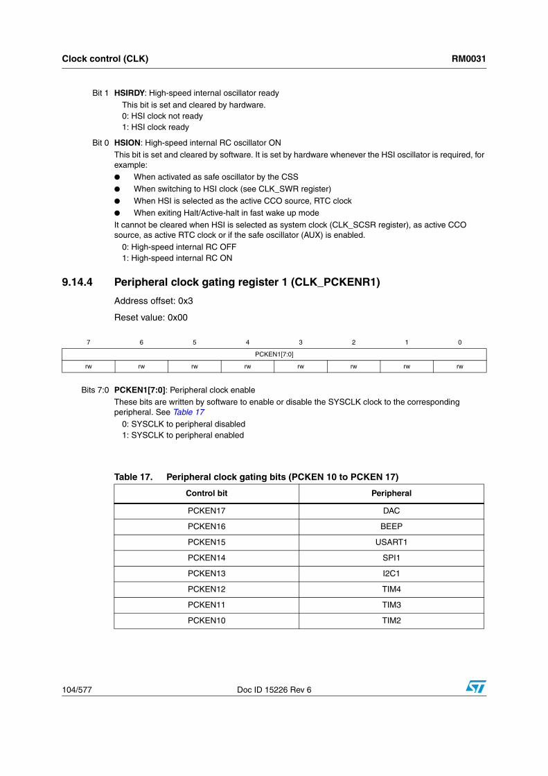
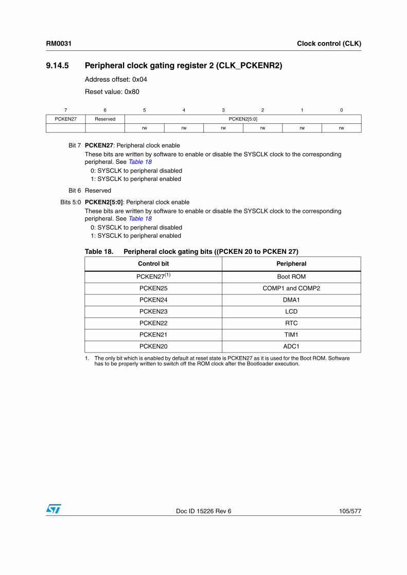
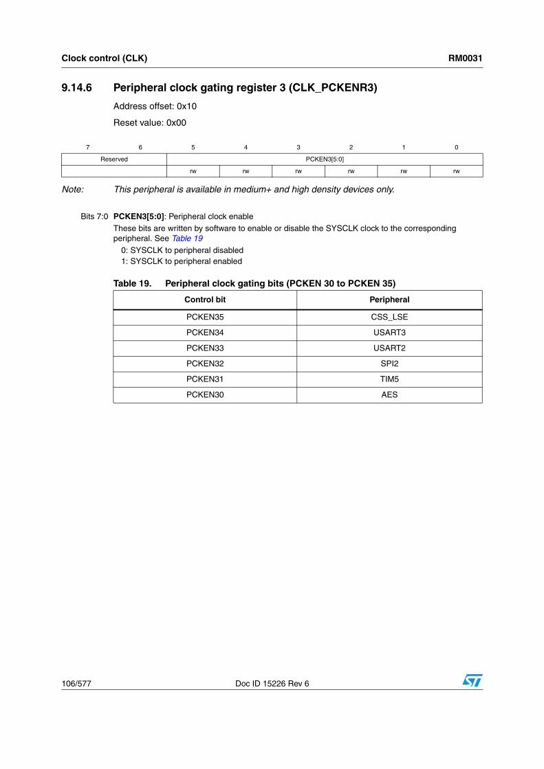
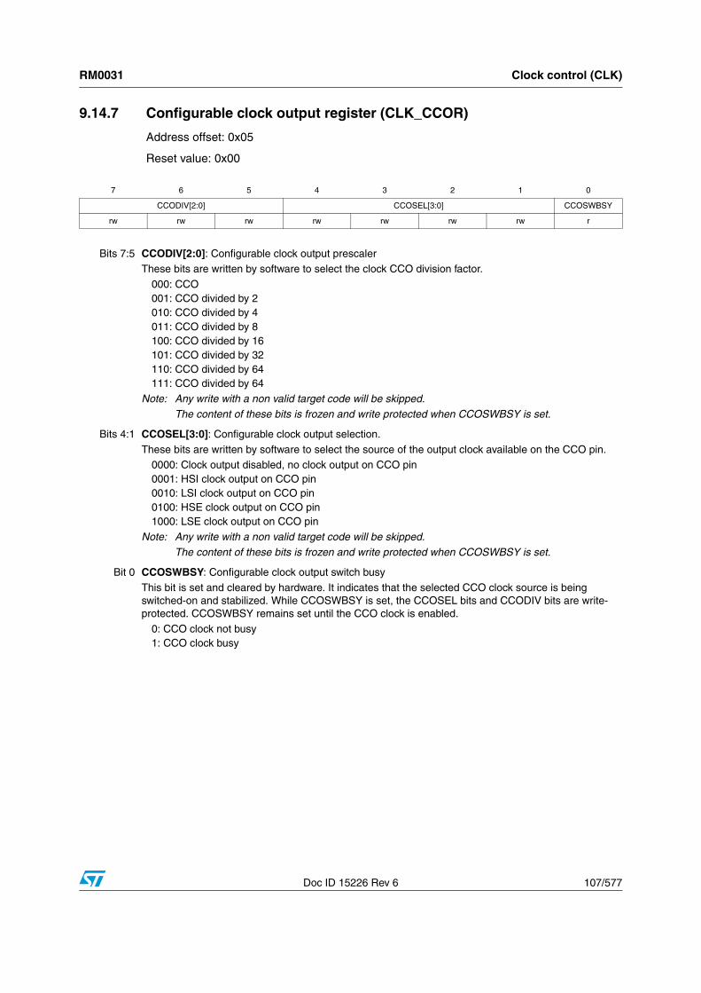
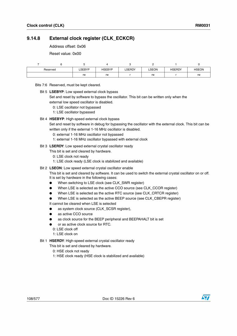
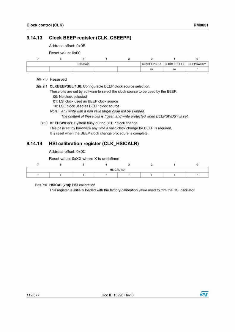
1.3 Global configuration register (CFG_GCR)
1.3.1 Activation level
The MCU activation level is configured by programming the AL bit in the CFG_GCR register.
For information on the use of this bit refer to Section 12.4: Activation level/low power mode control on page 149.
C 7 0
0 1 0 1 1 0 1 0 1
C 7 0
+ 0 1 0 0 1 0 1 0 0
C 7 0
= 1 0 1 0 0 1 0 0 1
Table 2. CPU register map
Addressoffset
Register name 7 6 5 4 3 2 1 0
0x00 A MSB - - - - - - LSB
0x01 PCE MSB --
- - - - LSB
0x02 PCH MSB - - - - - - LSB
0x03 PCL MSB - - - - - - LSB
0x04 XH MSB - - - - - - LSB
0x05 XL MSB - - - - - - LSB
0x06 YH MSB - - - - - - LSB
0x07 YL MSB - - - - - - LSB
0x08 SPH MSB - - - - - - LSB
0x09 SPL MSB - - - - - - LSB
0x0A CC V 0 I1 H I0 N Z C
RM0031 Central processing unit (CPU)
Doc ID 15226 Rev 6 35/577
1.3.2 SWIM disable
By default, after an MCU reset, the SWIM pin is configured to allow communication with an external tool for debugging or Flash/EEPROM programming. This pin can be configured by the application for use as a general purpose I/O. This is done by setting the SWD bit in the CFG_GCR register.
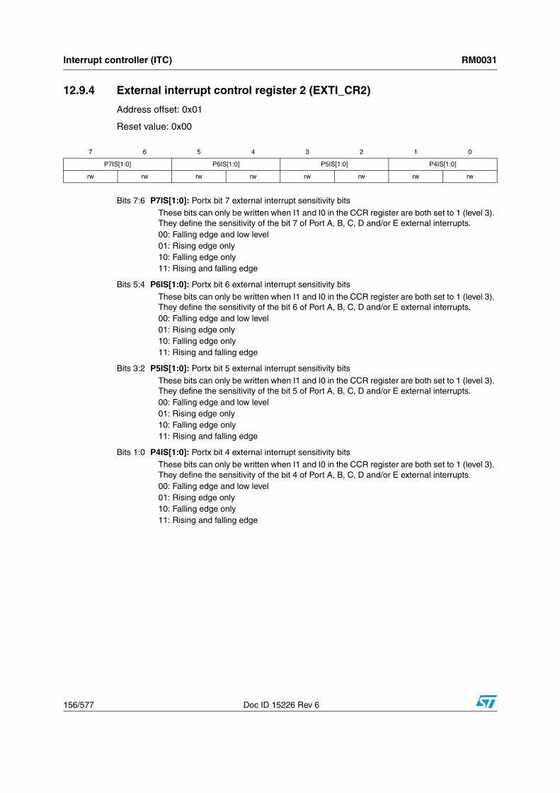
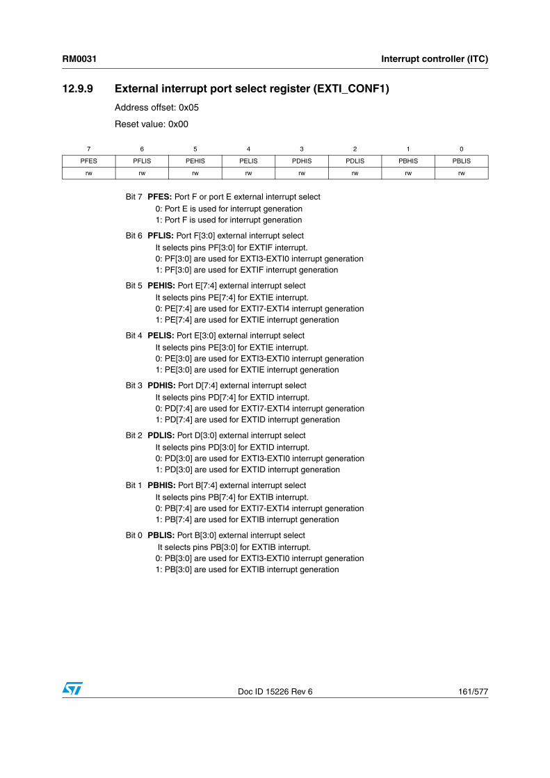
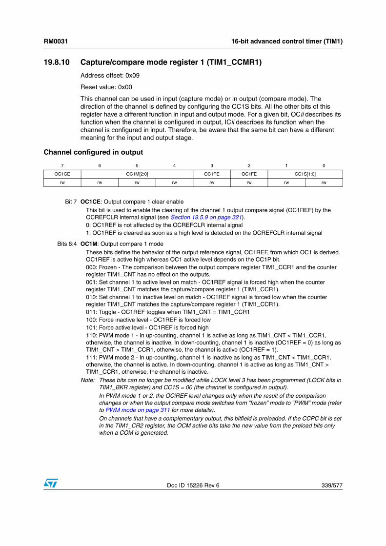
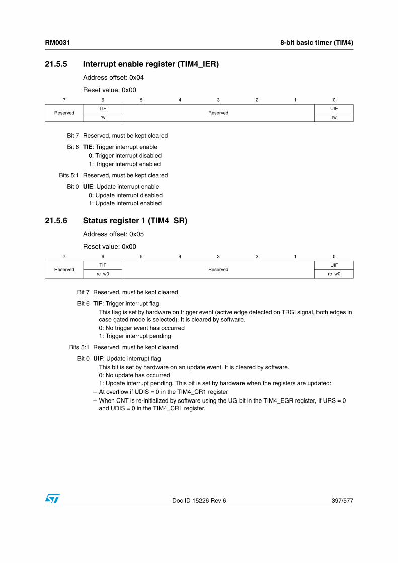
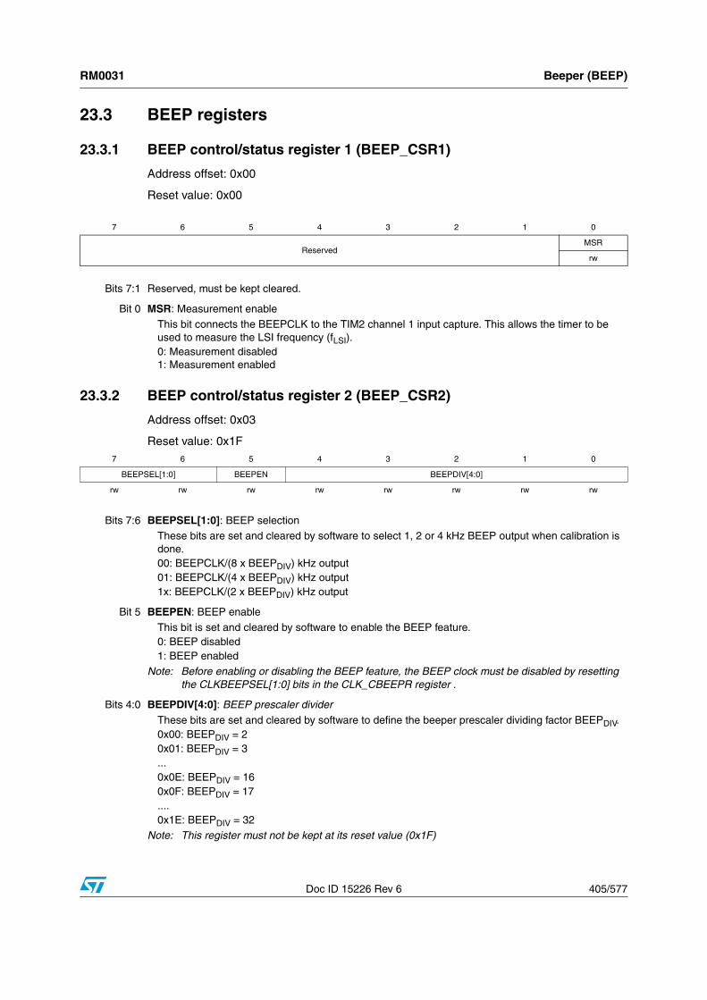
1.3.3 Description of global configuration register (CFG_GCR)
Address offset: 0x00
Reset value: 0x00
1.3.4 Global configuration register map and reset values
The CFG_GCR is mapped in the STM8 address space. Refer to the corresponding datasheets for the base address.
7 6 5 4 3 2 1 0
ReservedAL SWD
rw rw
Bits 7:2 Reserved, must be kept cleared.
Bit 1 AL: Activation level
This bit is set and cleared by software. It configures main or interrupt-only activation.0: Main activation level. An IRET instruction causes the context to be retrieved from the stack and the main program continues after the WFI instruction.1: Interrupt-only activation level. An IRET instruction causes the CPU to go back to WFI/halt mode without restoring the context.
Bit 0 SWD: SWIM disable
0: SWIM mode enabled1: SWIM mode disabled
When SWIM mode is enabled, the SWIM pin cannot be used as general purpose I/O.
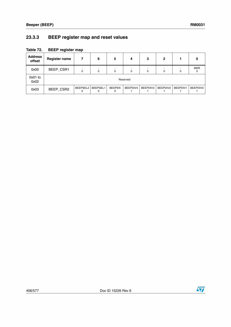
Table 3. CFG_GCR register map
Address offset
Register name 7 6 5 4 3 2 1 0
0x00CFG_GCRReset value
-0
-0
-0
-0
-0
-0
AL0
SWD0
Boot ROM RM0031
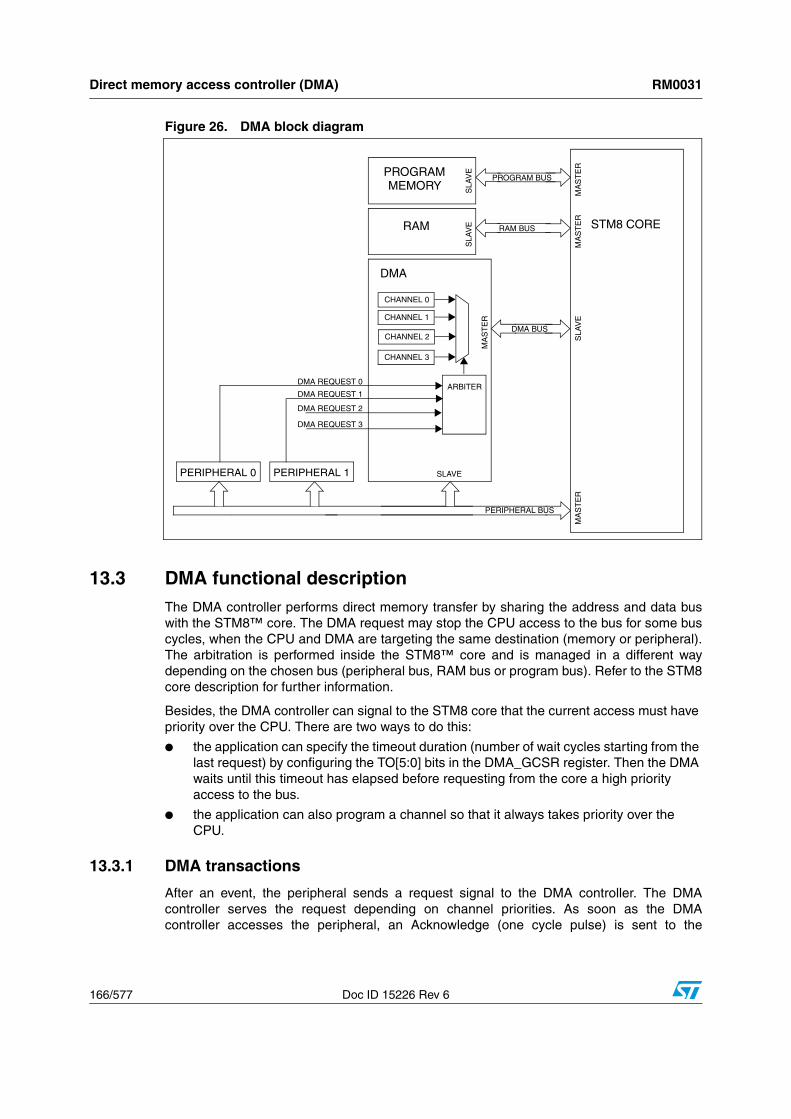
36/577 Doc ID 15226 Rev 6
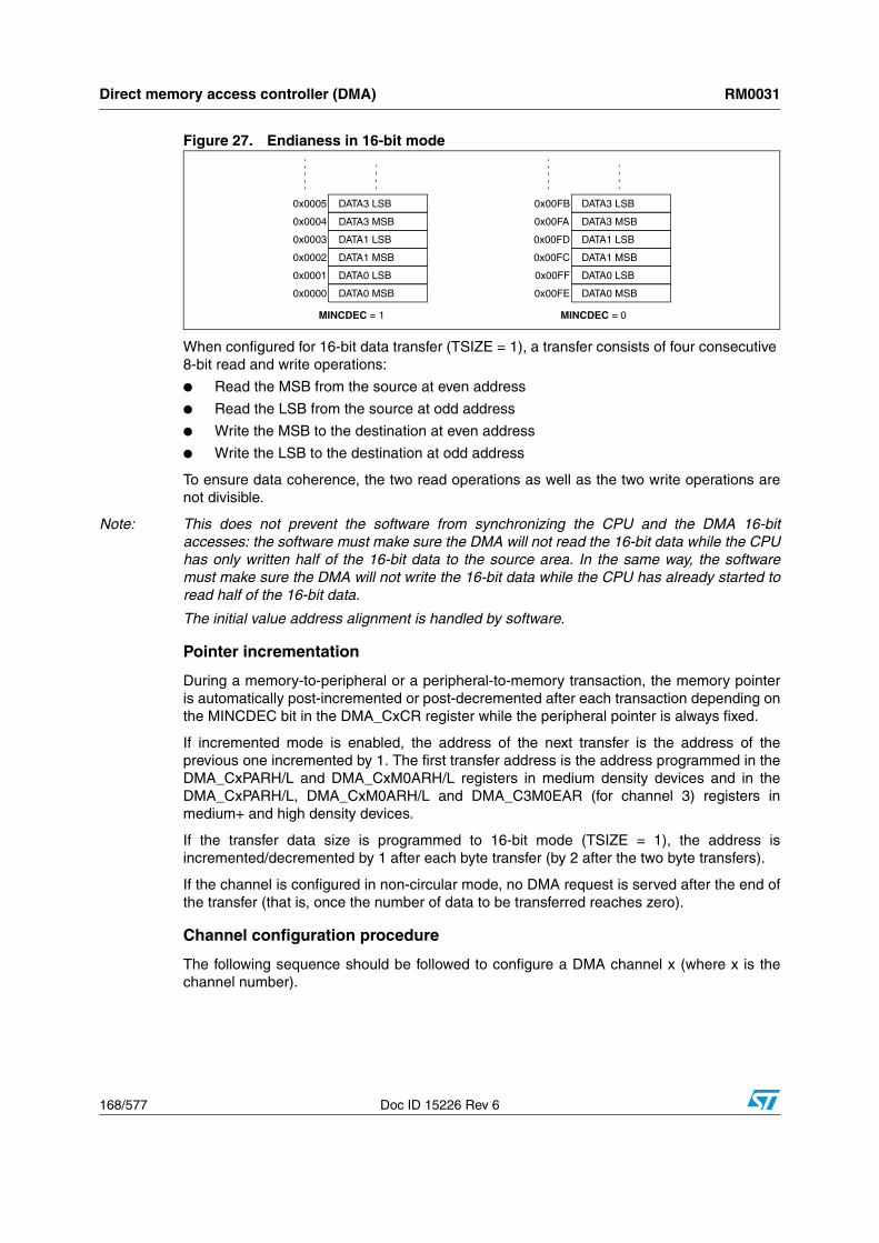
2 Boot ROM
This section applies to medium density STM8L15x devices, medium+ density STM8L15x devices and high density STM8L15x/STM8L16x devices, unless otherwise specified.
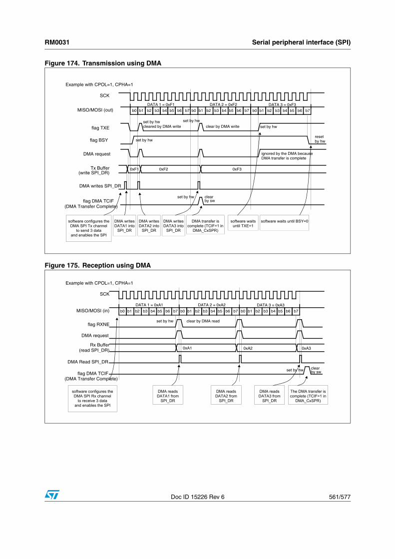
The internal 2 Kbyte boot ROM contains the bootloader code. Its main task is to download the application program to the internal Flash/EEPROM through the USART1, USART2, USART3 (USARTs in asynchronous mode), SPI1 or SPI2 interfaces and program the code, data, option bytes and interrupt vectors in the internal Flash/EEPROM.
The boot loader starts executing after reset. Refer to the STM8 bootloader user manual (UM0560) for more details.
RM0031 Flash program memory and data EEPROM (Flash)
Doc ID 15226 Rev 6 37/577
3 Flash program memory and data EEPROM (Flash)
This section applies to medium density STM8L15x devices, medium+ density STM8L15x devices and high density STM8L15x/STM8L16x devices, unless otherwise specified.
3.1 IntroductionThe embedded Flash program memory and data EEPROM memories are controlled by a common set of registers. Using these registers, the application can program or erase memory contents and set write protection. The application can also program the device option bytes.
3.2 Glossary● Block
A block is a set of bytes that can be programmed or erased in one single programming operation. Operations that are performed at block level are faster than standard programming and erasing. Refer to Table 4 for the details on block size.
● Page
A page is a set of blocks.
Dedicated option bytes can be used to configure, by increments of one page, the size of the user boot code and proprietary code (when available).
Flash program memory and data EEPROM (Flash) RM0031
38/577 Doc ID 15226 Rev 6
3.3 Flash main features● Medium and medium+ density STM8L15x EEPROM is divided into three memory
arrays (see Section 3.4: Memory organization for details on the memory mapping):
– Up to 32 Kbytes of embedded Flash program
– Up to 1 Kbyte of data EEPROM
– Up to 128 option bytes (one block)
Flash program and data EEPROM areas are controlled by a common set of registers, allowing the memory content to be programmed or erased, and write protection to be activated.
● High density STM8L15x/16x EEPROM is divided into three memory arrays (see Section 3.4: Memory organization for details on the memory mapping):
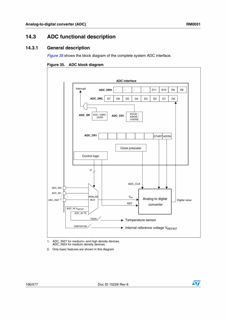
– 64 Kbytes of embedded Flash program
– Up to 2 Kbyte of data EEPROM
– Up to 128 option bytes (one block)
Flash program and data EEPROM areas are controlled by a common set of registers, allowing the memory content to be programmed or erased, and write protection to be activated.
● Programming modes
– Byte programming and automatic fast byte programming (without erase operation)
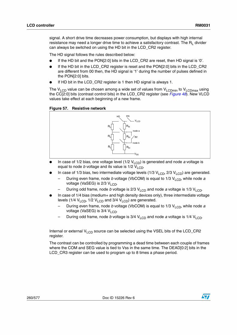
– Word programming
– Block programming and fast block programming mode (without erase operation)
– Interrupt generation on end of program/erase operation and on illegal program operation.
● Read-while-write capability (RWW)
● In-application programming (IAP) and in-circuit programming (ICP) capabilities
● Protection features
– Memory readout protection (ROP)
– Program memory write protection with memory access security system (MASS keys).
– Data memory write protection with memory access security system (MASS keys)
– Programmable write protected user boot code area (UBC)
– Automatic readout protection of proprietary code area when available
● Memory state configurable to operating or power-down mode (IDDQ) in wait mode (Low power wait) and Run mode (Low power run)
RM0031 Flash program memory and data EEPROM (Flash)
Doc ID 15226 Rev 6 39/577
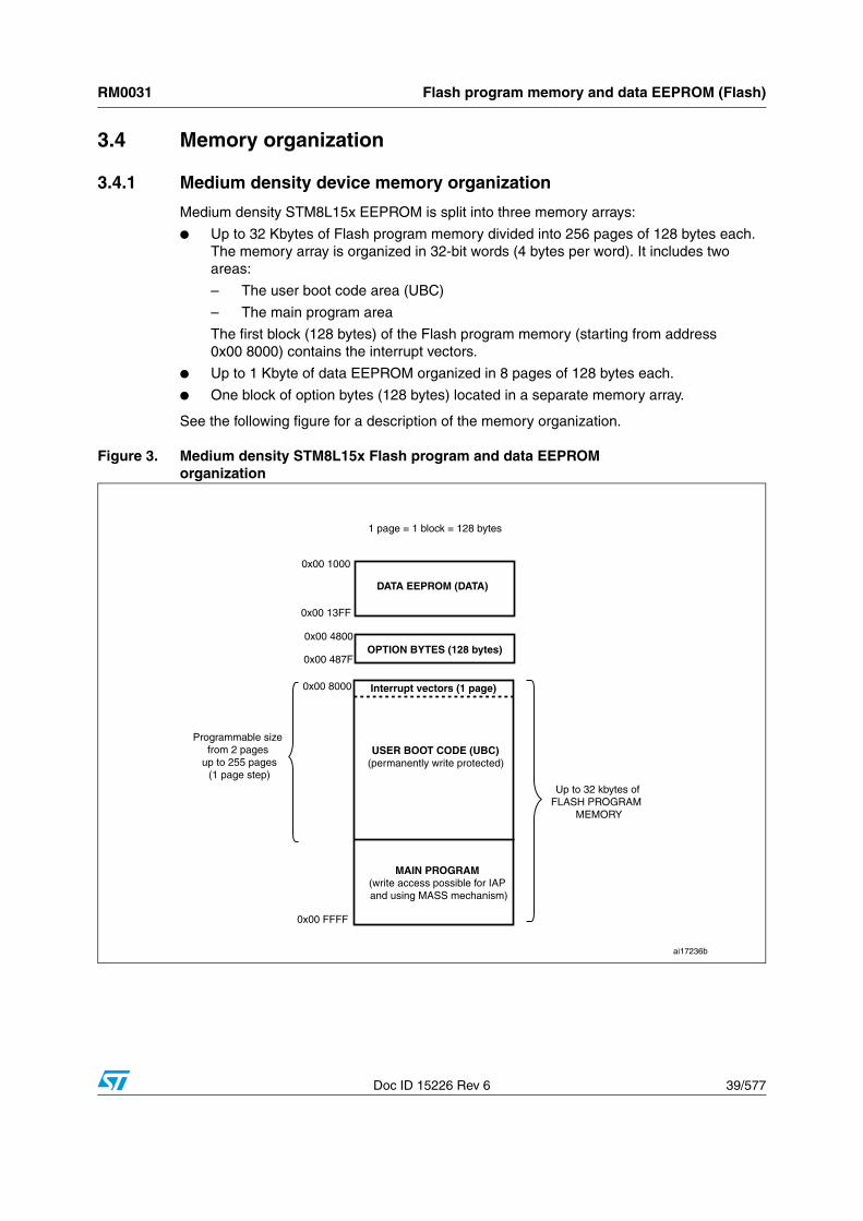
3.4 Memory organization
3.4.1 Medium density device memory organization
Medium density STM8L15x EEPROM is split into three memory arrays:
● Up to 32 Kbytes of Flash program memory divided into 256 pages of 128 bytes each. The memory array is organized in 32-bit words (4 bytes per word). It includes two areas:
– The user boot code area (UBC)
– The main program area
The first block (128 bytes) of the Flash program memory (starting from address 0x00 8000) contains the interrupt vectors.
● Up to 1 Kbyte of data EEPROM organized in 8 pages of 128 bytes each.
● One block of option bytes (128 bytes) located in a separate memory array.
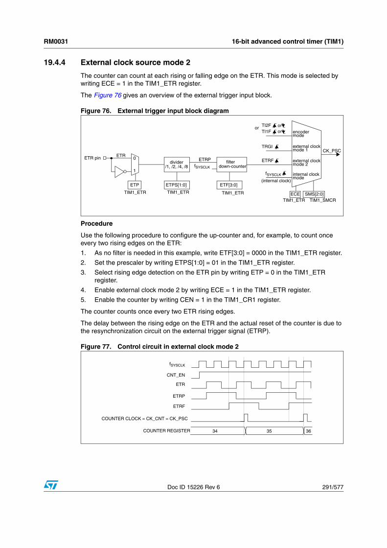
See the following figure for a description of the memory organization.
Figure 3. Medium density STM8L15x Flash program and data EEPROMorganization
Flash program memory and data EEPROM (Flash) RM0031
40/577 Doc ID 15226 Rev 6
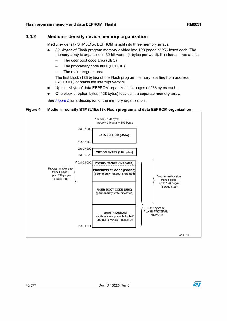
3.4.2 Medium+ density device memory organization
Medium+ density STM8L15x EEPROM is split into three memory arrays:
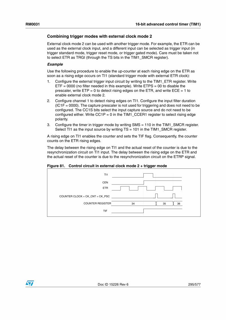
● 32 Kbytes of Flash program memory divided into 128 pages of 256 bytes each. The memory array is organized in 32-bit words (4 bytes per word). It includes three areas:
– The user boot code area (UBC)
– The proprietary code area (PCODE)
– The main program area
The first block (128 bytes) of the Flash program memory (starting from address 0x00 8000) contains the interrupt vectors.
● Up to 1 Kbyte of data EEPROM organized in 4 pages of 256 bytes each.
● One block of option bytes (128 bytes) located in a separate memory array.
See Figure 5 for a description of the memory organization.
Figure 4. Medium+ density STM8L15x/16x Flash program and data EEPROM organization
RM0031 Flash program memory and data EEPROM (Flash)
Doc ID 15226 Rev 6 41/577
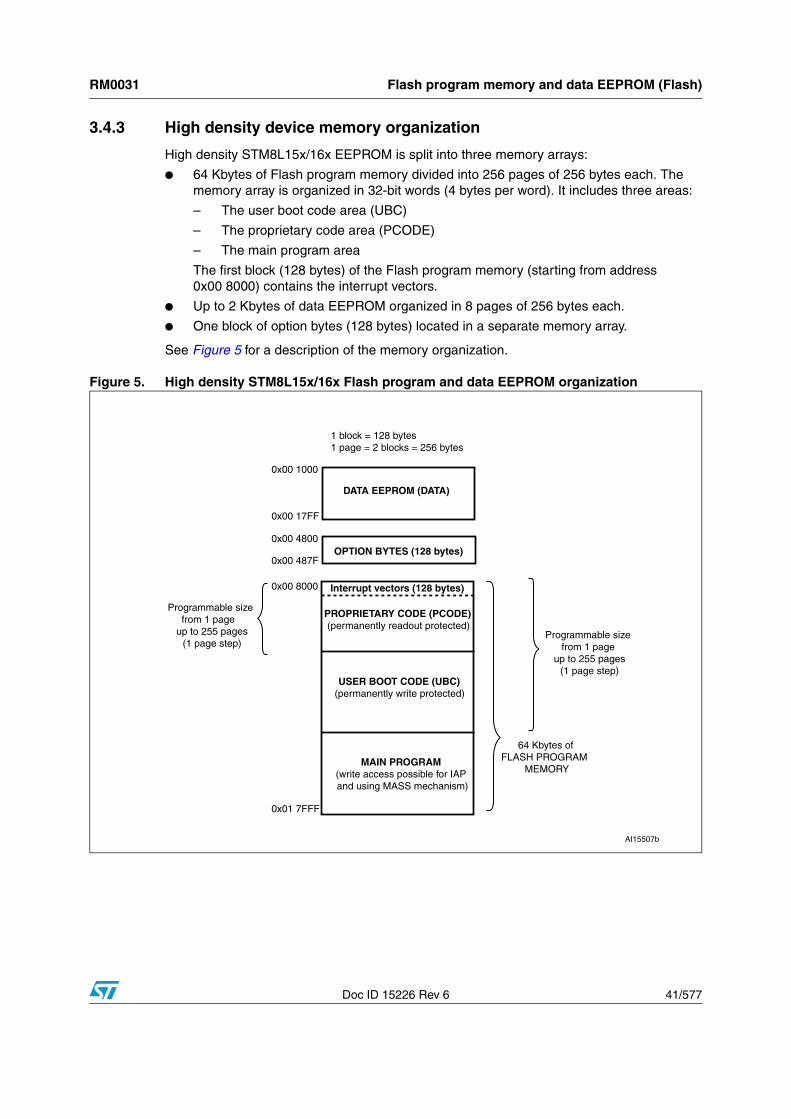
3.4.3 High density device memory organization
High density STM8L15x/16x EEPROM is split into three memory arrays:
● 64 Kbytes of Flash program memory divided into 256 pages of 256 bytes each. The memory array is organized in 32-bit words (4 bytes per word). It includes three areas:
– The user boot code area (UBC)
– The proprietary code area (PCODE)
– The main program area
The first block (128 bytes) of the Flash program memory (starting from address 0x00 8000) contains the interrupt vectors.
● Up to 2 Kbytes of data EEPROM organized in 8 pages of 256 bytes each.
● One block of option bytes (128 bytes) located in a separate memory array.
See Figure 5 for a description of the memory organization.
Figure 5. High density STM8L15x/16x Flash program and data EEPROM organization
Flash program memory and data EEPROM (Flash) RM0031
42/577 Doc ID 15226 Rev 6
3.4.4 Proprietary code area (PCODE)
The proprietary code area (PCODE) can be used to protect proprietary software libraries used to drive peripherals. It is available only in medium + and high density devices.
The size of the PCODE area can be configured through the PCODE option byte (PCODESIZE) in ICP mode (using the SWIM interface). This option byte specifies the number of pages (256-byte granularity) allocated for the PCODE area starting from address 0x00 8000. Once programmed, the PCODE option byte cannot be erased, and the size of the PCODE area remains fixed.
The minimum meaningful size of the PCODE area is of 1 page (256 bytes) of which 128 bytes are used to store the interrupt vectors.
In medium+ density devices, the maximum size of the PCODE area is 128 pages ranging from address 0x00 8000 to 0x00 FFFF. In high density devices, the maximum size of the PCODE area is 255 pages ranging from address 0x00 8000 to 0x01 7EFF.
The PCODE area is automatically readout protected except for the interrupt vectors TRAP and TLI (see Section 3.5.1: Readout protection and Table 5: Memory access versus programming method (medium+ and high density devices)). The readout protection cannot be disabled in this area. This means that the content of the PCODE area cannot be read or modified.
The PCODE area can be read only through the TRAP and TLI vectors.
3.4.5 User boot area (UBC)
The user boot area (UBC) contains the reset and the interrupt vectors. It can be used to store the IAP and communication routines. The UBC area has a second level of protection to prevent unintentional erasing or modification during IAP programming. This means that it is always write protected and the write protection cannot be unlocked using the MASS keys.
The size of the UBC area can be obtained by reading the UBC option byte.
The size of the UBC area can be configured in ICP mode (using the SWIM interface) through the UBC option byte. The UBC option byte specifies the number of pages allocated for the UBC area starting from address 0x00 8000.
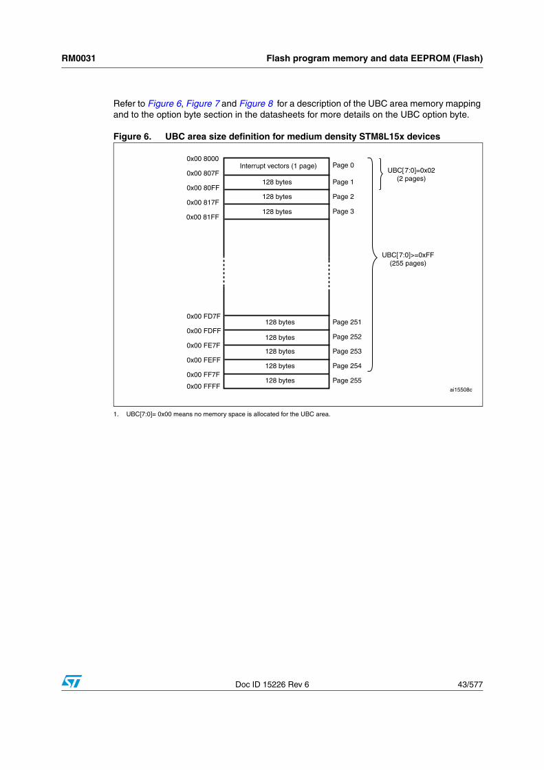
In medium density STM8L15x devices, the minimum meaningful size of the UBC area is of 2 pages of which 1 is used to store the interrupt vectors.
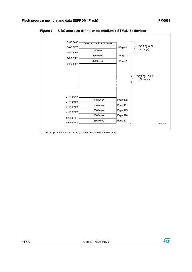
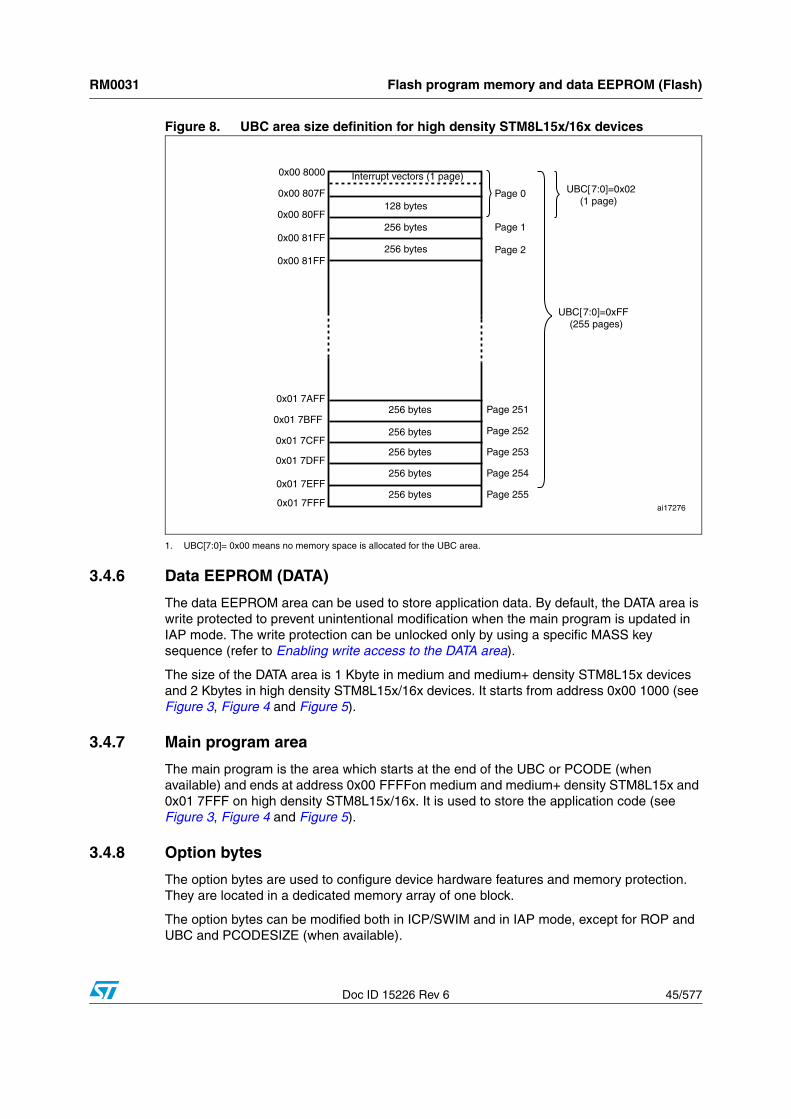
In medium+ and high density devices, the minimum meaningful size of the UBC area is of 1 page of which 128 bytes are used to store the interrupt vectors.
Note: When a PCODE area has been defined, the minimum size of the UBC should be PCODESIZE+1. The portion of the UBC available to store the boot code is the area located between the end of the PCODE area and the end of the defined UBC area.
In high density STM8L15x/16x devices, the maximum size of the boot area is 255 pages ranging from address 0x00 8000 to 0x01 7EFF (including the interrupt vectors).
In medium+ density STM8L15x devices, the maximum size of the boot area is 128 pages ranging from address 0x00 8000 to 0x00 FFFF (including the interrupt vectors)."
In medium density STM8L15x devices, the maximum size of the boot area is 255 pages ranging from address 0x00 8000 to 0x00 FF7F(including the interrupt vectors).
RM0031 Flash program memory and data EEPROM (Flash)
Doc ID 15226 Rev 6 43/577
Refer to Figure 6, Figure 7 and Figure 8 for a description of the UBC area memory mapping and to the option byte section in the datasheets for more details on the UBC option byte.
Figure 6. UBC area size definition for medium density STM8L15x devices
1. UBC[7:0]= 0x00 means no memory space is allocated for the UBC area.
Flash program memory and data EEPROM (Flash) RM0031
44/577 Doc ID 15226 Rev 6
Figure 7. UBC area size definition for medium + STM8L15x devices
1. UBC[7:0]= 0x00 means no memory space is allocated for the UBC area.
RM0031 Flash program memory and data EEPROM (Flash)
Doc ID 15226 Rev 6 45/577
Figure 8. UBC area size definition for high density STM8L15x/16x devices
1. UBC[7:0]= 0x00 means no memory space is allocated for the UBC area.
3.4.6 Data EEPROM (DATA)
The data EEPROM area can be used to store application data. By default, the DATA area is write protected to prevent unintentional modification when the main program is updated in IAP mode. The write protection can be unlocked only by using a specific MASS key sequence (refer to Enabling write access to the DATA area).
The size of the DATA area is 1 Kbyte in medium and medium+ density STM8L15x devices and 2 Kbytes in high density STM8L15x/16x devices. It starts from address 0x00 1000 (see Figure 3, Figure 4 and Figure 5).
3.4.7 Main program area
The main program is the area which starts at the end of the UBC or PCODE (when available) and ends at address 0x00 FFFFon medium and medium+ density STM8L15x and 0x01 7FFF on high density STM8L15x/16x. It is used to store the application code (see Figure 3, Figure 4 and Figure 5).
3.4.8 Option bytes
The option bytes are used to configure device hardware features and memory protection. They are located in a dedicated memory array of one block.
The option bytes can be modified both in ICP/SWIM and in IAP mode, except for ROP and UBC and PCODESIZE (when available).
Flash program memory and data EEPROM (Flash) RM0031
46/577 Doc ID 15226 Rev 6
Refer to the option byte section in the datasheet for more information on option bytes, and to the STM8 SWIM protocol and debug module user manual (UM0470) for details on how to program them.
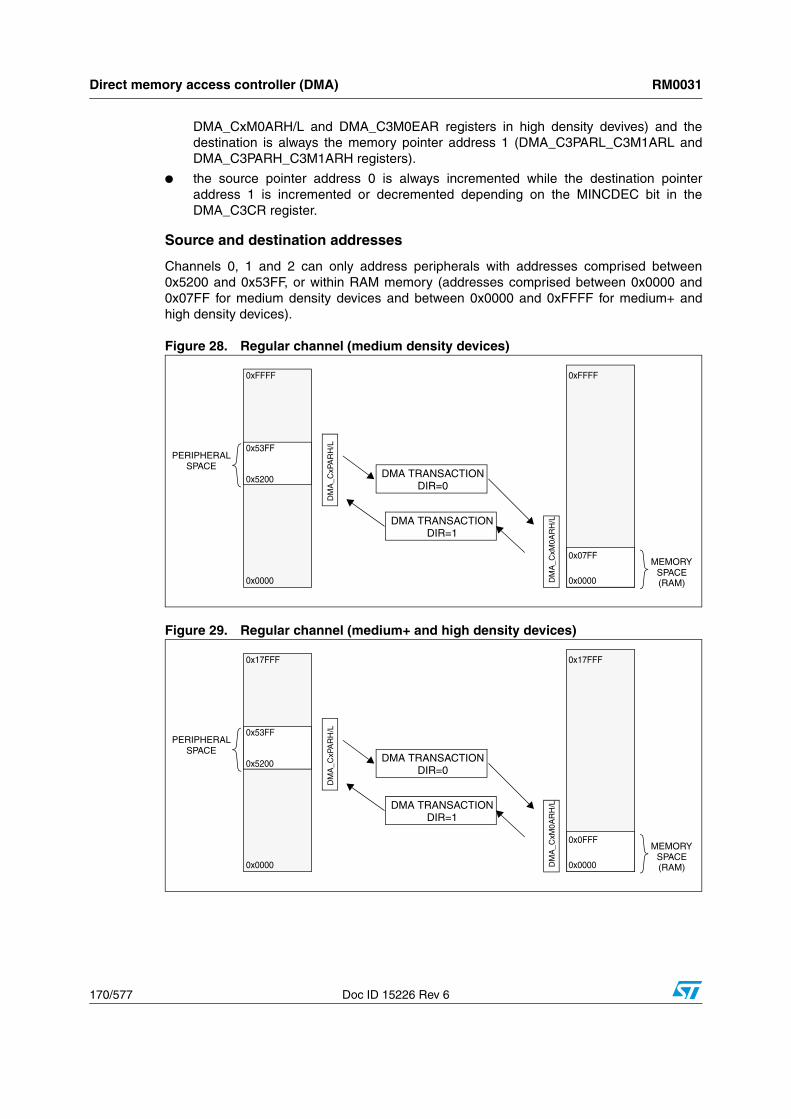
3.5 Memory protection
3.5.1 Readout protection
Readout protection is removed by programming the ROP option byte to 0xAA. When readout protection is enabled, reading or modifying the Flash program memory and DATA area in ICP mode (using the SWIM interface) is forbidden, whatever the write protection settings. Even if no protection can be considered as totally unbreakable, the readout feature provides a very high level of protection for a general purpose microcontroller.
The readout protection can be disabled on the program memory, UBC, PCODE (when available), and DATA areas, by reprogramming the ROP option byte in ICP mode. In this case, the Flash program memory, the DATA area and the option bytes are automatically erased and the device can be reprogrammed.
By default, the PCODE area is always readout protected except for the interrupt vectors TRAP and TLI (see Section 3.4.4: Proprietary code area (PCODE)).
Refer to Table 6: Memory access versus programming method (medium density devices) for details on memory access when readout protection is enabled or disabled.
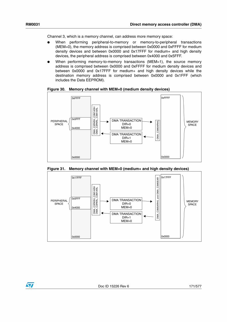
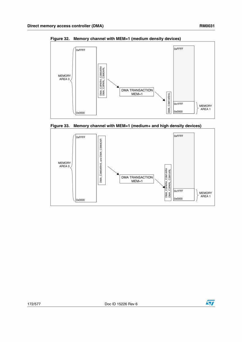
3.5.2 Memory access security system (MASS)
After reset, the main program and DATA areas are protected against unintentional write operations. They must be unlocked before attempting to modify their content. This unlock mechanism is managed by the memory access security system (MASS).
The UBC area specified in the UBC option byte is always write protected (see Section 3.4.5: User boot area (UBC)).
Once the memory has been modified, it is recommended to enable the write protection again to protect the memory content against corruption.
Enabling write access to the main program memory
After a device reset, it is possible to disable the main program memory write protection by writing consecutively two values called MASS keys to the FLASH_PUKR register (see Section 3.9.3: Flash program memory unprotecting key register (FLASH_PUKR)). These programmed keys are then compared to two hardware key values:
● First hardware key: 0b0101 0110 (0x56)
● Second hardware key: 0b1010 1110 (0xAE)
The following steps are required to disable write protection of the main program area:
RM0031 Flash program memory and data EEPROM (Flash)
Doc ID 15226 Rev 6 47/577
1. Write a first 8-bit key into the FLASH_PUKR register. When this register is written for the first time after a reset, the data bus content is not latched into the register, but compared to the first hardware key value (0x56).
2. If the key available on the data bus is incorrect, the FLASH_PUKR register remains locked until the next reset. Any new write commands sent to this address are discarded.
3. If the first hardware key is correct when the FLASH_PUKR register is written for the second time, the data bus content is still not latched into the register, but compared to the second hardware key value (0xAE).
4. If the key available on the data bus is incorrect, the write protection on program memory remains locked until the next reset. Any new write commands sent to this address is discarded.
5. If the second hardware key is correct, the main program memory is write unprotected and the PUL bit of the FLASH_IAPSR is set (see Section 3.9.5: Flash status register (FLASH_IAPSR) register.
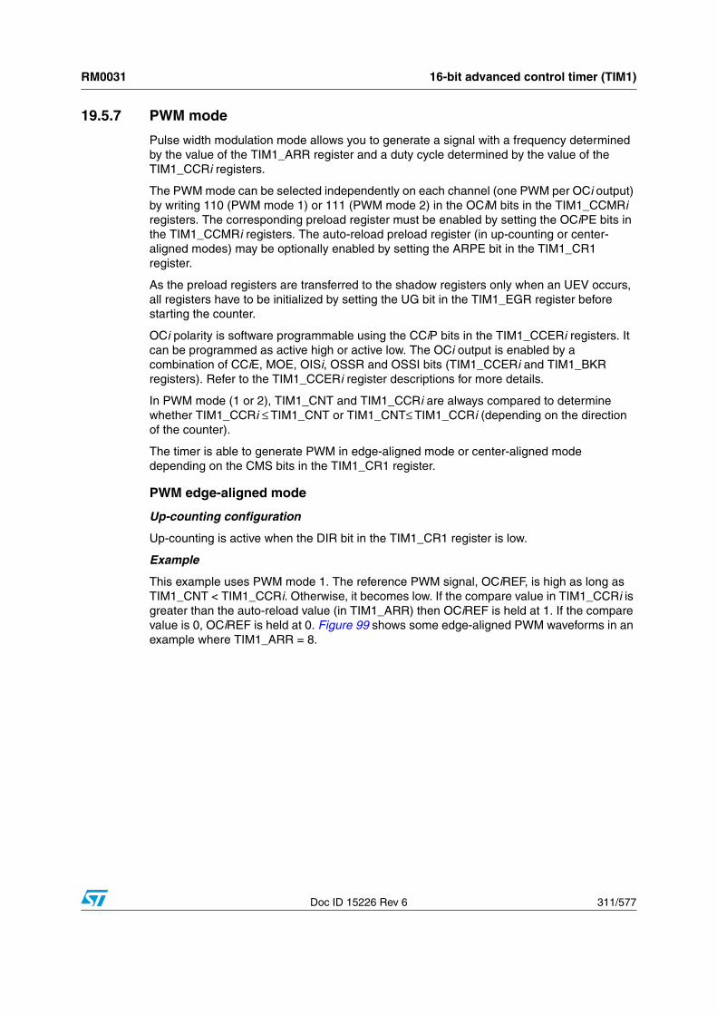
Before starting programming, the application must verify that PUL bit is effectively set. The application can choose, at any time, to disable again write access to the Flash program memory by clearing the PUL bit.
Enabling write access to the DATA area
After a device reset, it is possible to disable the DATA area write protection by writing consecutively two values called MASS keys to the FLASH_DUKR register (see Section 3.9.6: Flash register map and reset values). These programmed keys are then compared to two hardware key values:
● First hardware key: 0b1010 1110 (0xAE)
● Second hardware key: 0b0101 0110 (0x56)
The following steps are required to disable write protection of the DATA area:
1. Write a first 8-bit key into the FLASH_DUKR register. When this register is written for the first time after a reset, the data bus content is not latched into the register, but compared to the first hardware key value (0xAE).
2. If the key available on the data bus is incorrect, the application can re-enter two MASS keys to try unprotecting the DATA area.
3. If the first hardware key is correct, the FLASH_DUKR register is programmed with the second key. The data bus content is still not latched into the register, but compared to the second hardware key value (0x56).
4. If the key available on the data bus is incorrect, the data EEPROM area remains write protected until the next reset. Any new write command sent to this address is ignored.
5. If the second hardware key is correct, the DATA area is write unprotected and the DUL bit of the FLASH_IAPSR register is set (see Section 3.9.5: Flash status register (FLASH_IAPSR)).
Before starting programming, the application must verify that the DATA area is not write protected by checking that the DUL bit is effectively set. The application can choose, at any time, to disable again write access to the DATA area by clearing the DUL bit.
3.5.3 Enabling write access to option bytes
The write access to the option byte area can be enabled by setting the OPT bit in the Flash control register 2 (FLASH_CR2).
Flash program memory and data EEPROM (Flash) RM0031
48/577 Doc ID 15226 Rev 6
3.6 Memory programmingThe main program memory, and the DATA area must be unlocked before attempting to perform any program operation. The unlock mechanism depends on the memory area to be programmed as described in Section 3.5.2: Memory access security system (MASS).
Note: The PCODE area is always readout protected. The only way to reprogram it is to reset the ROP option byte, thus erasing the Flash program memory, DATA area, and option bytes.
3.6.1 Read-while-write (RWW)
The RWW feature allows write operations to be performed on data EEPROM while reading and executing the program memory. Execution time is therefore optimized. The opposite operation is not allowed: Data memory cannot be read while writing to the program memory.
This RWW feature is always enabled and can be used at any time.
3.6.2 Byte programming
The main program memory and the DATA area can be programmed at byte level. To program one byte, the application writes directly to the target address.
● In the main program memory:
The application stops for the duration of the byte program operation.
● In DATA area:
– Program execution stops during the “End of high voltage” operation, that is when the HVOFF flag is set, and the byte program operation is performed using the read-while-write (RWW) capability in IAP mode.
To erase a byte, simply write 0x00 at the corresponding address.
The application can read the FLASH_IAPSR register to verify that the programming or erasing operation has been correctly executed:
● EOP flag is set after a successful programming operation
● WR_PG_DIS is set when the software has tried to write to a protected page. In this case, the write procedure is not performed.
As soon as one of these flags are set, a Flash interrupt is generated if it has been previously enabled by setting the IE bit of the FLASH_CR1 register.
RM0031 Flash program memory and data EEPROM (Flash)
Doc ID 15226 Rev 6 49/577
Automatic fast byte programming
The programming duration can vary according to the initial content of the target address. If the word (4 bytes) containing the byte to be programmed is not empty, the whole word is automatically erased before the program operation. On the contrary if the word is empty, no erase operation is performed and the programming time is shorter (see tPROG in Table “Flash program memory” in the datasheet).
However, the programming time can be fixed by setting the FIX bit of the FLASH_CR1 register to force the program operation to systematically erase the byte whatever its content (see Section 3.9.1: Flash control register 1 (FLASH_CR1)). The programming time is consequently fixed and equal to the sum of the erase and write time (see tPROG in Table “Flash program memory” in the datasheet).
Note: To write a byte fast (no erase), the whole word (4 bytes) into which it is written must be erased beforehand. Consequently, It is not possible to do two fast writes to the same word (without an erase before the second write): The first write will be fast but the second write to the other byte will require an erase.
3.6.3 Word programming
A word write operation allows an entire 4-byte word to be programmed in one shot, thus minimizing the programming time.
As for byte programming, word operation is available both for the main program memory and data EEPROM. The read-while-write (RWW) capability is also available when a word programming operation is performed on the data EEPROM. Refer to the datasheets for additional information.
● In the main program memory:
The application stops for the duration of the byte program operation.
● In DATA area:
– Program execution does not stop, and the byte program operation is performed using the read-while-write (RWW) capability in IAP mode.
To program a word, the WPRG bit in the FLASH_CR2 register must be previously set to enable word programming mode (see Section 3.9.2: Flash control register 2 (FLASH_CR2)). Then, the 4 bytes of the word to be programmed must be loaded starting with the first address. The programming cycle starts automatically when the 4 bytes have been written.
As for byte operation, the EOP and the WR_PG_DIS control flags of FLASH_IAPSR, together with the Flash interrupt, can be used to determine if the operation has been correctly completed.
Flash program memory and data EEPROM (Flash) RM0031
50/577 Doc ID 15226 Rev 6
3.6.4 Block programming
Block program operations are much faster than byte or word program operations. In a block program operation, a whole block is programmed or erased in a single programming cycle. Refer to Table 4 for details on the block size according to the devices.
Block operations can be performed both to the main program memory and DATA area:
● In the main program memory:
Block program operations to the main program memory have to be executed totally from RAM.
● In the DATA area
– DATA block operations can be executed from the main program memory. However, the data loading phase (see below) has to be executed from RAM.
There are three possible block operations:
● Block programming, also called standard block programming: The block is automatically erased before being programmed.
● Fast block programming: No previous erase operation is performed.
● Block erase
During block programming, interrupts are masked by hardware.
Standard block programming
A standard block program operation allows a whole block to be written in one shot. The block is automatically erase before being programmed.
To program a whole block in standard mode, the PRG bit in the FLASH_CR2 register must be previously set to enable standard block programming (see Section 3.9.2: Flash control register 2 (FLASH_CR2)). Then, the block of data to be programmed must be loaded sequentially to the destination addresses in the main program memory or DATA area. This causes all the bytes of data to be latched. To start programming the whole block, all bytes of data must be written. All bytes written in a programming sequence must be in the same block. This means that they must have the same high address: Only the six least significant bits of the address can change. When the last byte of the target block is loaded, the programming starts automatically. It is preceded by an automatic erase operation of the whole block.
The EOP and the WR_PG_DIS control flags of the FLASH_IAPSR together with the Flash interrupt can be used to determine if the operation has been correctly completed.
RM0031 Flash program memory and data EEPROM (Flash)
Doc ID 15226 Rev 6 51/577
Fast block programming
Fast block programming allows programming without first erasing the memory contents. Fast block programming is therefore twice as fast as standard programming.
This mode is intended only for programming parts that have already been erased. It is very useful for programming blank parts with the complete application code, as the time saving is significant.
Fast block programming is performed by using the same sequence as standard block programming. To enable fast block programming mode, the FPRG bit of the FLASH_CR2 registers must be previously set.
The EOP and WR_PG_DIS bits of the FLASH_IAPSR register can be checked to determine if the fast block programming operation has been correctly completed.
Caution: The data programmed in the block are not guaranteed when the block is not blank before the fast block program operation.
Block erasing
A block erase allows a whole block to be erased.
To erase a whole block, the ERASE bit in the FLASH_CR2 register must be previously set to enable block erasing (see Section 3.9.2: Flash control register 2 (FLASH_CR2)). The block is then erased by writing ‘0x00 00 00 00’ to any word inside the block. The word start address must end with ‘0’, ‘4’, ‘8’, or ‘C’.
The EOP and the WR_PG_DIS control flags of the FLASH_IAPSR together with the Flash interrupt can be used to determine if the operation has been correctly completed.
3.6.5 Option byte programming
Option byte programming is very similar to data EEPROM byte programming.
The application writes directly to the target address. The program does not stop and the write operation is performed using the RWW capability.
Refer to the datasheet for details of the option byte contents.
3.7 Flash low power modesAll STM8L15x/16x Flash program memory and data EEPROM have one low consumption mode, IDDQ. In IDDQ mode, the memory is switched off. It is used for any of the device low power modes: Halt, active-halt, low power wait, and low power run.
Table 4. Block size
STM8 microcontroller family Block size
Medium density STM8L15x 128 bytes
Medium+ density STM8L15x 128 bytes
High density STM8L15x/16x 128 bytes
Flash program memory and data EEPROM (Flash) RM0031
52/577 Doc ID 15226 Rev 6
When the EEPM bit is set in FLASH_CR1 register, the Flash program memory and data EEPROM automatically enter IDDQ mode when the code is executed from RAM or when the device is in Wait mode.
Refer to Section 3.9.1: Flash control register 1 (FLASH_CR1) for details on WAITM and EEPM bits.
When the Flash program memory and data EEPROM exit from IDDQ mode, the recovery time is lower than 2.8 µs and depends on supply voltage and temperature.
RM0031 Flash program memory and data EEPROM (Flash)
Doc ID 15226 Rev 6 53/577
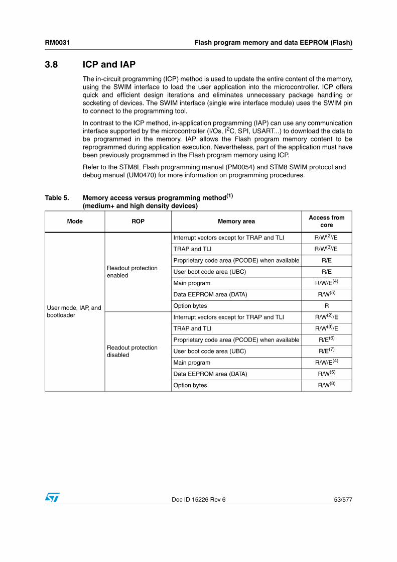
3.8 ICP and IAPThe in-circuit programming (ICP) method is used to update the entire content of the memory,using the SWIM interface to load the user application into the microcontroller. ICP offersquick and efficient design iterations and eliminates unnecessary package handling orsocketing of devices. The SWIM interface (single wire interface module) uses the SWIM pinto connect to the programming tool.
In contrast to the ICP method, in-application programming (IAP) can use any communicationinterface supported by the microcontroller (I/Os, I2C, SPI, USART...) to download the data tobe programmed in the memory. IAP allows the Flash program memory content to bereprogrammed during application execution. Nevertheless, part of the application must havebeen previously programmed in the Flash program memory using ICP.
Refer to the STM8L Flash programming manual (PM0054) and STM8 SWIM protocol and debug manual (UM0470) for more information on programming procedures.
Table 5. Memory access versus programming method(1) (medium+ and high density devices)
Mode ROP Memory areaAccess from
core
User mode, IAP, and bootloader
Readout protection enabled
Interrupt vectors except for TRAP and TLI R/W(2)/E
TRAP and TLI R/W(3)/E
Proprietary code area (PCODE) when available R/E
User boot code area (UBC) R/E
Main program R/W/E(4)
Data EEPROM area (DATA) R/W(5)
Option bytes R
Readout protection disabled
Interrupt vectors except for TRAP and TLI R/W(2)/E
TRAP and TLI R/W(3)/E
Proprietary code area (PCODE) when available R/E(6)
User boot code area (UBC) R/E(7)
Main program R/W/E(4)
Data EEPROM area (DATA) R/W(5)
Option bytes R/W(8)
Flash program memory and data EEPROM (Flash) RM0031
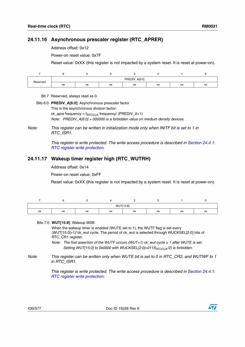
54/577 Doc ID 15226 Rev 6
SWIM active(ICP mode)
Readout protection enabled
Interrupt vectors except for TRAP and TLI P
TRAP and TLI P
Proprietary code area (PCODE) when available P(6)
User boot code area (UBC) P
Main program P
Data EEPROM area (DATA) P
Option bytes P/WROP(9)
Readout protection disabled
Interrupt vectors except for TRAP and TLI R/W(2)/E
TRAP and TLI R/W/E
Proprietary code area (PCODE) when available R/E(6)
User boot code area (UBC) R/E(7)
Main program R/W/E(4)
Data EEPROM area (DATA) R/W(5)
Option bytes R/W(8)
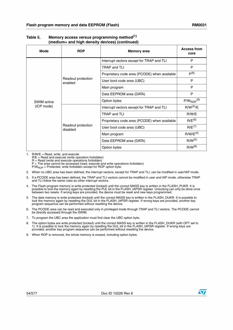
1. R/W/E = Read, write, and execute R/E = Read and execute (write operation forbidden) R = Read (write and execute operations forbidden) P = The area cannot be accessed (read, execute and write operations forbidden)P/WROP = Protected, write forbidden except for ROP option byte.
2. When no UBC area has been defined, the interrupt vectors, except for TRAP and TLI, can be modified in user/IAP mode.
3. If a PCODE area has been defined, the TRAP and TLI vectors cannot be modified in user and IAP mode, otherwise TRAP and TLI follow the same rules as other interrupt vectors.
4. The Flash program memory is write protected (locked) until the correct MASS key is written in the FLASH_PUKR. It is possible to lock the memory again by resetting the PUL bit in the FLASH_IAPSR register. Unlocking can only be done once between two resets. If wrong keys are provided, the device must be reset and new keys programmed.
5. The data memory is write protected (locked) until the correct MASS key is written in the FLASH_DUKR. It is possible to lock the memory again by resetting the DUL bit in the FLASH_IAPSR register. If wrong keys are provided, another key program sequence can be performed without resetting the device.
6. The PCODE area can be read and executed only in privileged mode through TRAP and TLI vectors. The PCODE cannot be directly accessed through the SWIM.
7. To program the UBC area the application must first clear the UBC option byte.
8. The option bytes are write protected (locked) until the correct MASS key is written in the FLASH_DUKR (with OPT set to 1). It is possible to lock the memory again by resetting the DUL bit in the FLASH_IAPSR register. If wrong keys are provided, another key program sequence can be performed without resetting the device.
9. When ROP is removed, the whole memory is erased, including option bytes.
Table 5. Memory access versus programming method(1) (medium+ and high density devices) (continued)
Mode ROP Memory areaAccess from
core
RM0031 Flash program memory and data EEPROM (Flash)
Doc ID 15226 Rev 6 55/577
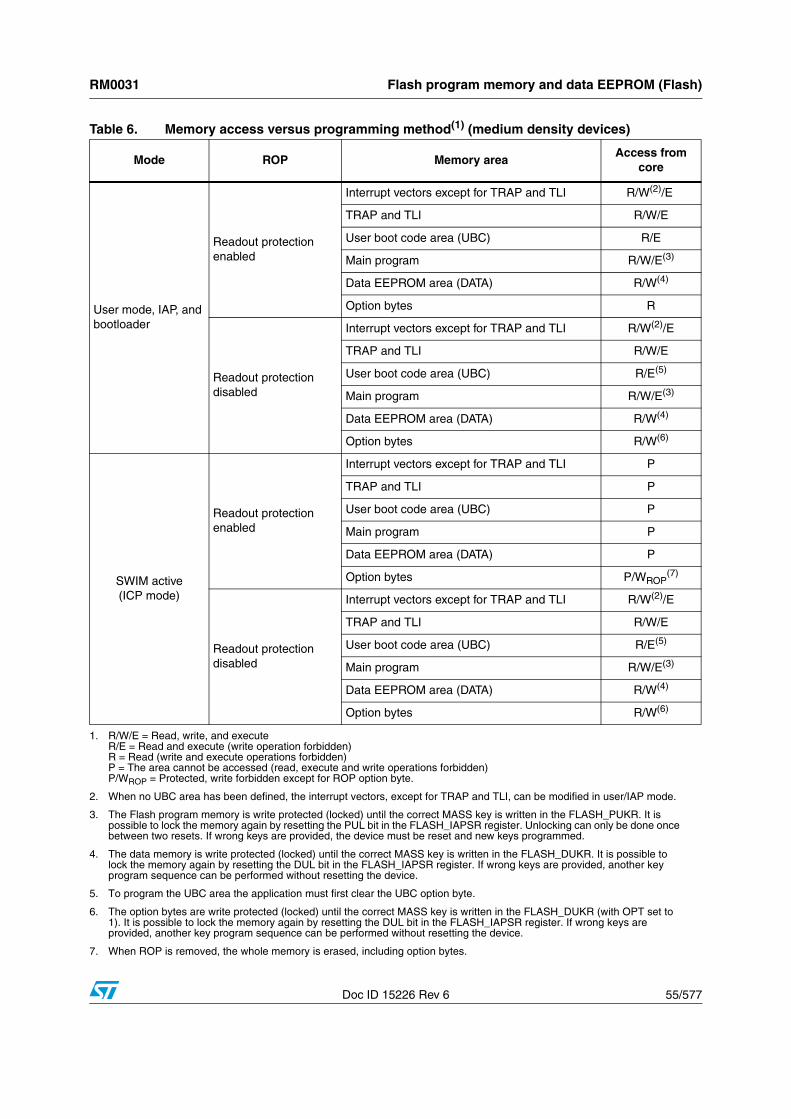
Table 6. Memory access versus programming method(1) (medium density devices)
Mode ROP Memory areaAccess from
core
User mode, IAP, and bootloader
Readout protection enabled
Interrupt vectors except for TRAP and TLI R/W(2)/E
TRAP and TLI R/W/E
User boot code area (UBC) R/E
Main program R/W/E(3)
Data EEPROM area (DATA) R/W(4)
Option bytes R
Readout protection disabled
Interrupt vectors except for TRAP and TLI R/W(2)/E
TRAP and TLI R/W/E
User boot code area (UBC) R/E(5)
Main program R/W/E(3)
Data EEPROM area (DATA) R/W(4)
Option bytes R/W(6)
SWIM active(ICP mode)
Readout protection enabled
Interrupt vectors except for TRAP and TLI P
TRAP and TLI P
User boot code area (UBC) P
Main program P
Data EEPROM area (DATA) P
Option bytes P/WROP(7)
Readout protection disabled
Interrupt vectors except for TRAP and TLI R/W(2)/E
TRAP and TLI R/W/E
User boot code area (UBC) R/E(5)
Main program R/W/E(3)
Data EEPROM area (DATA) R/W(4)
Option bytes R/W(6)
1. R/W/E = Read, write, and execute R/E = Read and execute (write operation forbidden) R = Read (write and execute operations forbidden) P = The area cannot be accessed (read, execute and write operations forbidden)P/WROP = Protected, write forbidden except for ROP option byte.
2. When no UBC area has been defined, the interrupt vectors, except for TRAP and TLI, can be modified in user/IAP mode.
3. The Flash program memory is write protected (locked) until the correct MASS key is written in the FLASH_PUKR. It is possible to lock the memory again by resetting the PUL bit in the FLASH_IAPSR register. Unlocking can only be done once between two resets. If wrong keys are provided, the device must be reset and new keys programmed.
4. The data memory is write protected (locked) until the correct MASS key is written in the FLASH_DUKR. It is possible to lock the memory again by resetting the DUL bit in the FLASH_IAPSR register. If wrong keys are provided, another key program sequence can be performed without resetting the device.
5. To program the UBC area the application must first clear the UBC option byte.
6. The option bytes are write protected (locked) until the correct MASS key is written in the FLASH_DUKR (with OPT set to 1). It is possible to lock the memory again by resetting the DUL bit in the FLASH_IAPSR register. If wrong keys are provided, another key program sequence can be performed without resetting the device.
7. When ROP is removed, the whole memory is erased, including option bytes.
Flash program memory and data EEPROM (Flash) RM0031
56/577 Doc ID 15226 Rev 6
3.9 Flash registers
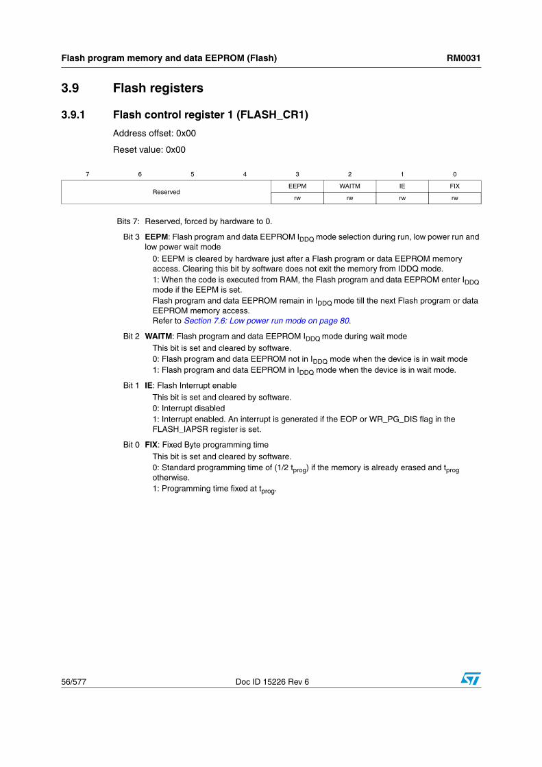
3.9.1 Flash control register 1 (FLASH_CR1)
Address offset: 0x00
Reset value: 0x00
7 6 5 4 3 2 1 0
ReservedEEPM WAITM IE FIX
rw rw rw rw
Bits 7: Reserved, forced by hardware to 0.
Bit 3 EEPM: Flash program and data EEPROM IDDQ mode selection during run, low power run and low power wait mode
0: EEPM is cleared by hardware just after a Flash program or data EEPROM memory access. Clearing this bit by software does not exit the memory from IDDQ mode.1: When the code is executed from RAM, the Flash program and data EEPROM enter IDDQ mode if the EEPM is set. Flash program and data EEPROM remain in IDDQ mode till the next Flash program or data EEPROM memory access.Refer to Section 7.6: Low power run mode on page 80.
Bit 2 WAITM: Flash program and data EEPROM IDDQ mode during wait modeThis bit is set and cleared by software.0: Flash program and data EEPROM not in IDDQ mode when the device is in wait mode1: Flash program and data EEPROM in IDDQ mode when the device is in wait mode.
Bit 1 IE: Flash Interrupt enableThis bit is set and cleared by software. 0: Interrupt disabled1: Interrupt enabled. An interrupt is generated if the EOP or WR_PG_DIS flag in the FLASH_IAPSR register is set.
Bit 0 FIX: Fixed Byte programming time
This bit is set and cleared by software. 0: Standard programming time of (1/2 tprog) if the memory is already erased and tprog otherwise. 1: Programming time fixed at tprog.
RM0031 Flash program memory and data EEPROM (Flash)
Doc ID 15226 Rev 6 57/577
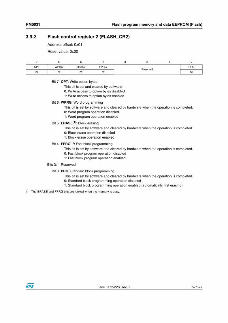
3.9.2 Flash control register 2 (FLASH_CR2)
Address offset: 0x01
Reset value: 0x00
7 6 5 4 3 2 1 0
OPT WPRG ERASE FPRGReserved
PRG
rw rw rw rw rw
Bit 7 OPT: Write option bytes
This bit is set and cleared by software. 0: Write access to option bytes disabled1: Write access to option bytes enabled
Bit 6 WPRG: Word programming
This bit is set by software and cleared by hardware when the operation is completed.0: Word program operation disabled1: Word program operation enabled
Bit 5 ERASE(1): Block erasingThis bit is set by software and cleared by hardware when the operation is completed. 0: Block erase operation disabled1: Block erase operation enabled
Bit 4 FPRG(1): Fast block programmingThis bit is set by software and cleared by hardware when the operation is completed.0: Fast block program operation disabled1: Fast block program operation enabled
Bits 3:1 Reserved
Bit 0 PRG: Standard block programming
This bit is set by software and cleared by hardware when the operation is completed.0: Standard block programming operation disabled1: Standard block programming operation enabled (automatically first erasing)
1. The ERASE and FPRG bits are locked when the memory is busy.
Flash program memory and data EEPROM (Flash) RM0031
58/577 Doc ID 15226 Rev 6
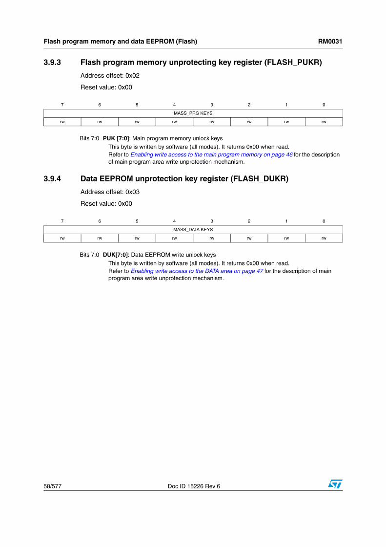
3.9.3 Flash program memory unprotecting key register (FLASH_PUKR)
Address offset: 0x02
Reset value: 0x00
3.9.4 Data EEPROM unprotection key register (FLASH_DUKR)
Address offset: 0x03
Reset value: 0x00
7 6 5 4 3 2 1 0
MASS_PRG KEYS
rw rw rw rw rw rw rw rw
Bits 7:0 PUK [7:0]: Main program memory unlock keys
This byte is written by software (all modes). It returns 0x00 when read. Refer to Enabling write access to the main program memory on page 46 for the description of main program area write unprotection mechanism.
7 6 5 4 3 2 1 0
MASS_DATA KEYS
rw rw rw rw rw rw rw rw
Bits 7:0 DUK[7:0]: Data EEPROM write unlock keys
This byte is written by software (all modes). It returns 0x00 when read. Refer to Enabling write access to the DATA area on page 47 for the description of main program area write unprotection mechanism.
RM0031 Flash program memory and data EEPROM (Flash)
Doc ID 15226 Rev 6 59/577
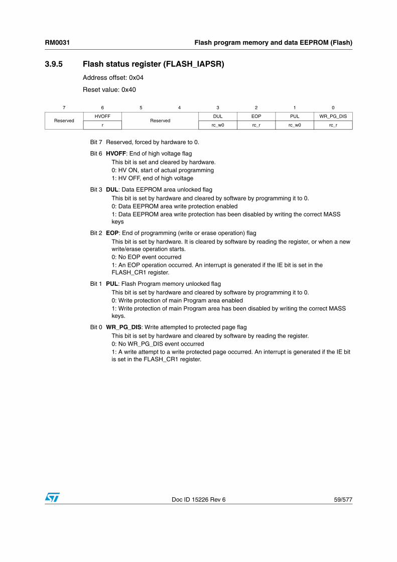
3.9.5 Flash status register (FLASH_IAPSR)
Address offset: 0x04
Reset value: 0x40
7 6 5 4 3 2 1 0
ReservedHVOFF
ReservedDUL EOP PUL WR_PG_DIS
r rc_w0 rc_r rc_w0 rc_r
Bit 7 Reserved, forced by hardware to 0.
Bit 6 HVOFF: End of high voltage flagThis bit is set and cleared by hardware.0: HV ON, start of actual programming1: HV OFF, end of high voltage
Bit 3 DUL: Data EEPROM area unlocked flagThis bit is set by hardware and cleared by software by programming it to 0. 0: Data EEPROM area write protection enabled1: Data EEPROM area write protection has been disabled by writing the correct MASS keys
Bit 2 EOP: End of programming (write or erase operation) flag
This bit is set by hardware. It is cleared by software by reading the register, or when a new write/erase operation starts.0: No EOP event occurred1: An EOP operation occurred. An interrupt is generated if the IE bit is set in the FLASH_CR1 register.
Bit 1 PUL: Flash Program memory unlocked flag
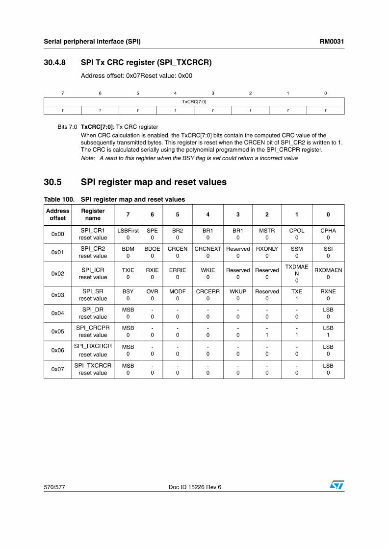
This bit is set by hardware and cleared by software by programming it to 0. 0: Write protection of main Program area enabled1: Write protection of main Program area has been disabled by writing the correct MASS keys.
Bit 0 WR_PG_DIS: Write attempted to protected page flag
This bit is set by hardware and cleared by software by reading the register. 0: No WR_PG_DIS event occurred1: A write attempt to a write protected page occurred. An interrupt is generated if the IE bit is set in the FLASH_CR1 register.
Flash program memory and data EEPROM (Flash) RM0031
60/577 Doc ID 15226 Rev 6
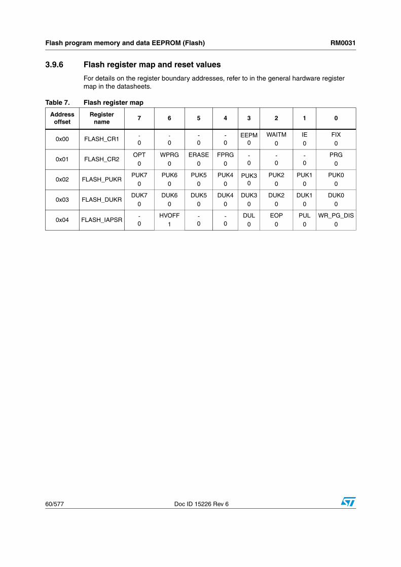
3.9.6 Flash register map and reset values
For details on the register boundary addresses, refer to in the general hardware register map in the datasheets.
Table 7. Flash register map
Address offset
Register name
7 6 5 4 3 2 1 0
0x00 FLASH_CR1-
0-
0-0
-0
EEPM0
WAITM0
IE0
FIX0
0x01 FLASH_CR2OPT
0WPRG
0ERASE
0FPRG
0-0
-0
-0
PRG0
0x02 FLASH_PUKRPUK7
0PUK6
0PUK5
0PUK4
0PUK3
0PUK2
0PUK1
0PUK0
0
0x03 FLASH_DUKRDUK7
0DUK6
0DUK5
0DUK4
0DUK3
0DUK2
0DUK1
0DUK0
0
0x04 FLASH_IAPSR-0
HVOFF
1-0
-0
DUL
0
EOP
0
PUL
0
WR_PG_DIS
0
RM0031 Single wire interface module (SWIM) and debug module (DM)
Doc ID 15226 Rev 6 61/577
4 Single wire interface module (SWIM) and debug module (DM)
This section applies to medium density STM8L15x devices, medium+ density STM8L15x devices and high density STM8L15x/STM8L16x devices, unless otherwise specified.
4.1 Introduction In-circuit debugging mode or in-circuit programming mode are managed through a single wire hardware interface featuring ultrafast memory programming. Coupled with an in-circuit debugging module, it also offers a non-intrusive emulation mode, making the in-circuit debugger extremely powerful, close in performance to a full-featured emulator.
4.2 Main features● Based on an asynchronous, high sink (8 mA), open-drain, bidirectional communication.
● Allows reading or writing any part of memory space.
● Access to CPU registers (A, X, Y, CC, SP). They are memory mapped for read or write access.
● Non intrusive read/write on the fly to the RAM and peripheral registers.
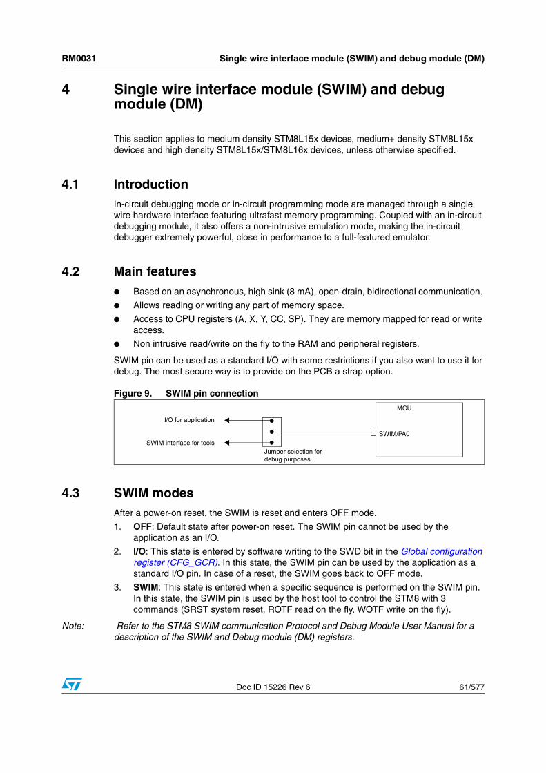
SWIM pin can be used as a standard I/O with some restrictions if you also want to use it for debug. The most secure way is to provide on the PCB a strap option.
Figure 9. SWIM pin connection
4.3 SWIM modesAfter a power-on reset, the SWIM is reset and enters OFF mode.
1. OFF: Default state after power-on reset. The SWIM pin cannot be used by the application as an I/O.
2. I/O: This state is entered by software writing to the SWD bit in the Global configuration register (CFG_GCR). In this state, the SWIM pin can be used by the application as a standard I/O pin. In case of a reset, the SWIM goes back to OFF mode.
3. SWIM: This state is entered when a specific sequence is performed on the SWIM pin. In this state, the SWIM pin is used by the host tool to control the STM8 with 3 commands (SRST system reset, ROTF read on the fly, WOTF write on the fly).
Note: Refer to the STM8 SWIM communication Protocol and Debug Module User Manual for a description of the SWIM and Debug module (DM) registers.
MCU
SWIM/PA0
Jumper selection for debug purposes
I/O for application
SWIM interface for tools
Memory and register map RM0031
62/577 Doc ID 15226 Rev 6
5 Memory and register map
This section applies to medium density STM8L15x devices, medium+ density STM8L15x devices and high density STM8L15x/STM8L16x devices, unless otherwise specified.
For details on the memory map, I/O port hardware register map and CPU/SWIM/debug module/interrupt controller registers, refer to the product datasheets.
5.1 Register description abbreviationsIn the register descriptions of each chapter in this reference manual, the following abbreviations are used:
read/write (rw) Software can read and write to these bits.
read-only (r) Software can only read these bits.
write only (w)Software can only write to this bit. Reading the bit returns a meaningless value.
read/write once (rwo)Software can only write once to this bit but, can read it at any time. Only a reset can return this bit to its reset value.
read/clear (rc_w1)Software can read and clear this bit by writing 1. Writing ‘0’ has no effect on the bit value.
read/clear (rc_w0)Software can read and clear this bit by writing 0. Writing ‘1’ has no effect on the bit value.
read/set (rs) Software can read and set this bit. Writing ‘0’ has no effect on the bit value.
read/clear by read (rc_r)
Software can read this bit. Reading this bit automatically clears it to ‘0’.
Writing ‘0’ has no effect on the bit value.
RM0031 Power control (PWR)
Doc ID 15226 Rev 6 63/577
6 Power control (PWR)
This section applies to medium density STM8L15x devices, medium+ density STM8L15x devices and high density STM8L15x/STM8L16x devices, unless otherwise specified.
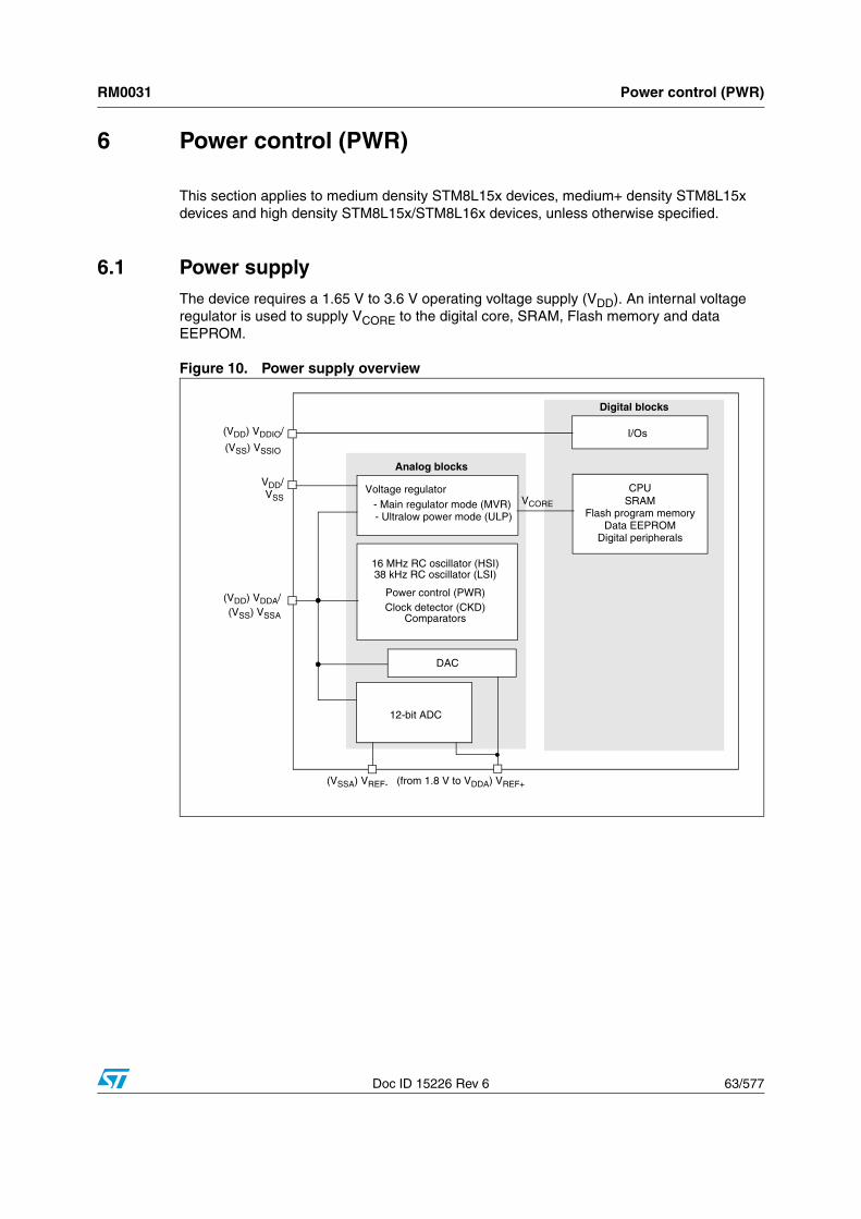
6.1 Power supplyThe device requires a 1.65 V to 3.6 V operating voltage supply (VDD). An internal voltage regulator is used to supply VCORE to the digital core, SRAM, Flash memory and data EEPROM.
Figure 10. Power supply overview
VDD/ Voltage regulator
I/Os
SRAMFlash program memory
CPU
Data EEPROM
(VDD) VDDIO/
(VDD) VDDA/
(from 1.8 V to VDDA) VREF+(VSSA) VREF-
Analog blocks
38 kHz RC oscillator (LSI)
12-bit ADC
Power control (PWR)Clock detector (CKD)
Comparators
16 MHz RC oscillator (HSI)
Digital peripherals
VCORE
DAC
- Main regulator mode (MVR) - Ultralow power mode (ULP)
Digital blocks
VSS
(VSS) VSSA
(VSS) VSSIO
Power control (PWR) RM0031
64/577 Doc ID 15226 Rev 6
External power supply pins:
The external power supply pins must be connected as follows:
● VSS; VDD = 1.8 to 3.6 V, down to 1.65 V at power-down: external power supply for I/Os and for the internal regulator. Provided externally through VDD pins, the corresponding ground pin is VSS.
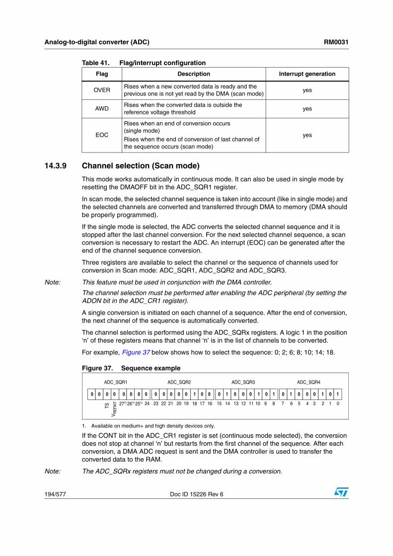
● VSSA; VDDA = 1.8 to 3.6 V, down to 1.65 V at power-down: external power supplies for analog peripherals (minimum voltage to be applied to VDDA is 1.8 V when the ADC1 is used). VDDA and VSSA must be connected to VDD and VSS, respectively.
● VSSIO; VDDIO = 1.8 to 3.6 V, down to 1.65 V at power-down: external power supplies for I/Os. VDDIO and VSSIO must be connected to VDD and VSS, respectively.
● VREF+; VREF- (for ADC1): external reference voltage for ADC1. Must be provided externally through VREF+ and VREF- pin.
● VREF+ (for DAC): external voltage reference for DAC must be provided externally through VREF+.
6.2 Power-on reset (POR)/power-down reset (PDR)The device has an integrated POR/PDR circuit which is permanently active. This eliminates the need for an external reset circuit. The POR/PDR thresholds are centered around 1.5 V (refer to the Electrical characteristics section in the product datasheet).
At power-on, the MCU is held in reset state until the power supply voltage is above the VPOR threshold. In medium density devices and in the medium+ and high density devices operating from 1.8V to 3.6V, the BOR (see paragraph below) starts to work above this threshold. At power-down, the MCU is held in reset state as soon as the supply voltage drops below the VPDR if the BOR is not active.
6.3 Brownout reset (BOR)For medium density devices and for medium+ and high density devices operating from 1.8 V to 3.6 V, the BOR is always active at power-on, keeping the MCU under reset till the application operating threshold is reached.
At power-down, the BOR threshold is also used to generate a reset.
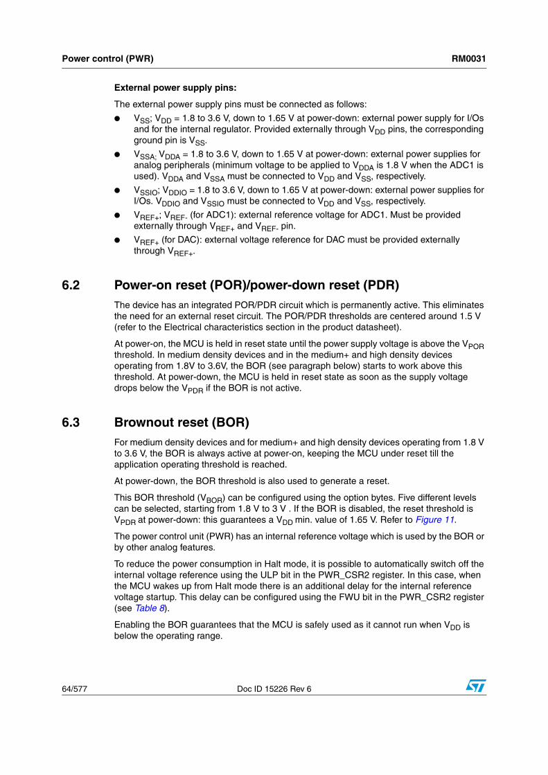
This BOR threshold (VBOR) can be configured using the option bytes. Five different levels can be selected, starting from 1.8 V to 3 V . If the BOR is disabled, the reset threshold is VPDR at power-down: this guarantees a VDD min. value of 1.65 V. Refer to Figure 11.
The power control unit (PWR) has an internal reference voltage which is used by the BOR or by other analog features.
To reduce the power consumption in Halt mode, it is possible to automatically switch off the internal voltage reference using the ULP bit in the PWR_CSR2 register. In this case, when the MCU wakes up from Halt mode there is an additional delay for the internal reference voltage startup. This delay can be configured using the FWU bit in the PWR_CSR2 register (see Table 8).
Enabling the BOR guarantees that the MCU is safely used as it cannot run when VDD is below the operating range.
RM0031 Power control (PWR)
Doc ID 15226 Rev 6 65/577
Figure 11. VDD voltage detection: BOR threshold
1. When BOR is disabled at power-down, this threshold is VPDR.
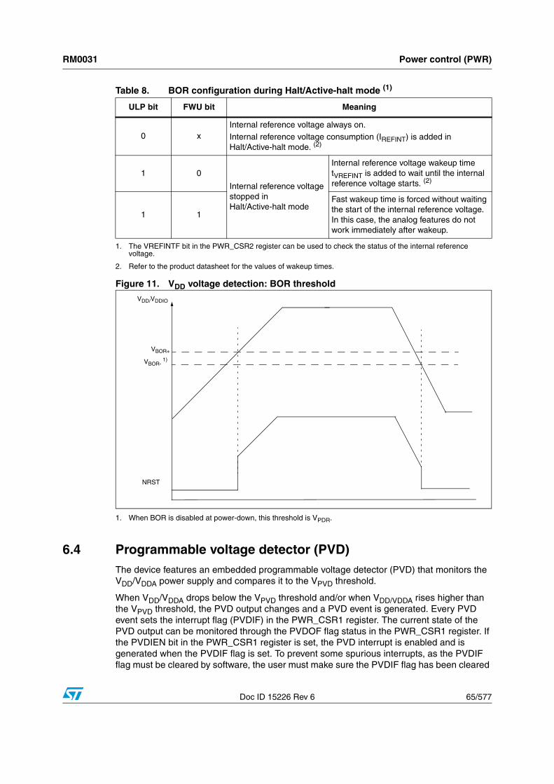
6.4 Programmable voltage detector (PVD)The device features an embedded programmable voltage detector (PVD) that monitors the VDD/VDDA power supply and compares it to the VPVD threshold.
When VDD/VDDA drops below the VPVD threshold and/or when VDD/VDDA rises higher than the VPVD threshold, the PVD output changes and a PVD event is generated. Every PVD event sets the interrupt flag (PVDIF) in the PWR_CSR1 register. The current state of the PVD output can be monitored through the PVDOF flag status in the PWR_CSR1 register. If the PVDIEN bit in the PWR_CSR1 register is set, the PVD interrupt is enabled and is generated when the PVDIF flag is set. To prevent some spurious interrupts, as the PVDIF flag must be cleared by software, the user must make sure the PVDIF flag has been cleared
Table 8. BOR configuration during Halt/Active-halt mode (1)
1. The VREFINTF bit in the PWR_CSR2 register can be used to check the status of the internal reference voltage.
ULP bit FWU bit Meaning
0 xInternal reference voltage always on.Internal reference voltage consumption (IREFINT) is added in Halt/Active-halt mode. (2)
2. Refer to the product datasheet for the values of wakeup times.
1 0
Internal reference voltage stopped in Halt/Active-halt mode
Internal reference voltage wakeup time tVREFINT is added to wait until the internal reference voltage starts. (2)
1 1
Fast wakeup time is forced without waiting the start of the internal reference voltage. In this case, the analog features do not work immediately after wakeup.
VDD/VDDIO
NRST
VBOR+
VBOR- 1)
Power control (PWR) RM0031
66/577 Doc ID 15226 Rev 6
before the PVD interrupt is enabled and before returning from the interrupt service. The PVD is enabled by software by setting the PVDE bit in the PWR_CSR1 register.
This PVD has 7 different levels between 1.85 V and 3.05 V, selected by the PLS[2:0] bits in the PWR_CSR1 register, in steps of around 200 mV. Refer to the “Power-up / power-down operating conditions” section in the product datasheet.
The external reference voltage on the PVD_IN input pin can be selected by setting the PLS[2:0] bits to 111.
Note: The voltage injected on PVD_IN (PE6) is compared to the VREFINT internal voltage reference.
Figure 12. PVD threshold
6.5 Voltage regulatorThe device has an internal voltage regulator for generating the 1.8 V power supply (VCORE) for the core and peripherals.
This regulator has two different modes:
● Main voltage regulator mode (MVR) for Run, Wait for interrupt (WFI) and Wait for event (WFE) modes.
● Ultralow power regulator mode (ULP) for Halt and Active-halt modes.
The regulator mode switches modes automatically, depending in some cases on some register control bits. Refer to Table 11.
RM0031 Power control (PWR)
Doc ID 15226 Rev 6 67/577
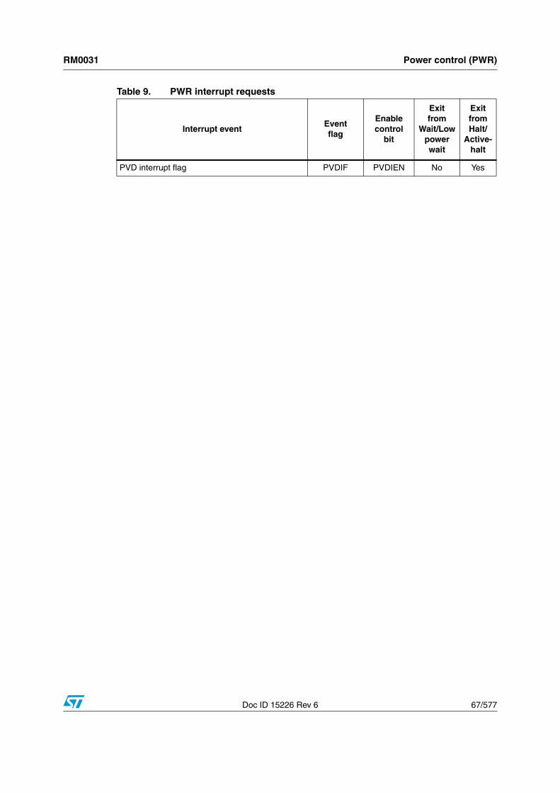
Table 9. PWR interrupt requests
Interrupt eventEventflag
Enable control
bit
Exit from
Wait/Low power wait
Exit from Halt/
Active-halt
PVD interrupt flag PVDIF PVDIEN No Yes
Power control (PWR) RM0031
68/577 Doc ID 15226 Rev 6
6.6 PWR registers
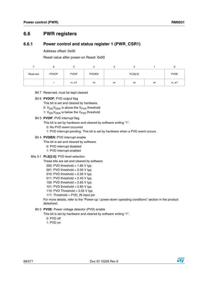
6.6.1 Power control and status register 1 (PWR_CSR1)
Address offset: 0x00
Reset value after power-on Reset: 0x00
7 6 5 4 3 2 1 0
Reserved PVDOF PVDIF PVDIEN PLS[2:0] PVDE
r rc_w1 rw rw rw rw rc_w1
Bit 7 Reserved, must be kept cleared.
Bit 6 PVDOF: PVD output flagThis bit is set and cleared by hardware.
0: VDD/VDDA is above the VPVD threshold
1: VDD/VDDA is below the VPVD threshold
Bit 5 PVDIF: PVD interrupt flag
This bit is set by hardware and cleared by software writing “1”.0: No PVD event occurred1: PVD interrupt pending. This bit is set by hardware when a PVD event occurs.
Bit 4 PVDIEN: PVD interrupt enableThis bit is set and cleared by software.
0: PVD interrupt disabled1: PVD interrupt enabled
Bits 3:1 PLS[2:0]: PVD level selection
These bits are set and cleared by software.
000: PVD threshold = 1.85 V typ.001: PVD threshold = 2.05 V typ.010: PVD threshold = 2.26 V typ.011: PVD threshold = 2.45 V typ.100: PVD threshold = 2.65 V typ.101: PVD threshold = 2.85 V typ.110: PVD Threshold = 3.05 V typ.111: Threshold = PVD_IN input pin
For more details, refer to the “Power-up / power-down operating conditions” section in the product datasheet.
Bit 0 PVDE: Power voltage detector (PVD) enable
This bit is set by hardware and cleared by software writing “1”.
0: PVD off1: PVD on
RM0031 Power control (PWR)
Doc ID 15226 Rev 6 69/577
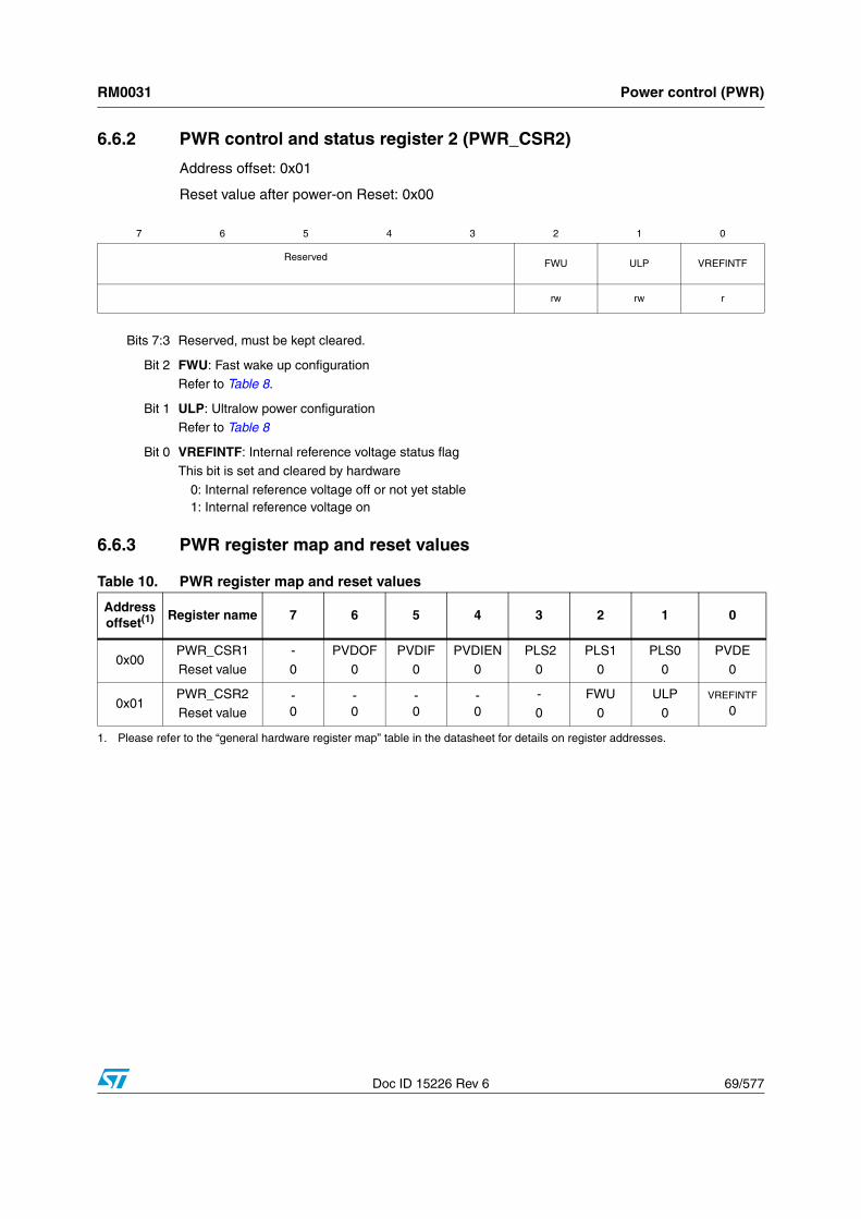
6.6.2 PWR control and status register 2 (PWR_CSR2)
Address offset: 0x01
Reset value after power-on Reset: 0x00
6.6.3 PWR register map and reset values
7 6 5 4 3 2 1 0
ReservedFWU ULP VREFINTF
rw rw r
Bits 7:3 Reserved, must be kept cleared.
Bit 2 FWU: Fast wake up configurationRefer to Table 8.
Bit 1 ULP: Ultralow power configurationRefer to Table 8
Bit 0 VREFINTF: Internal reference voltage status flagThis bit is set and cleared by hardware
0: Internal reference voltage off or not yet stable1: Internal reference voltage on
Table 10. PWR register map and reset values
Address offset(1) Register name 7 6 5 4 3 2 1 0
0x00PWR_CSR1
Reset value
-
0
PVDOF
0
PVDIF
0
PVDIEN
0
PLS2
0
PLS1
0
PLS0
0
PVDE
0
0x01PWR_CSR2
Reset value-0
-0
-0
-0
-
0
FWU
0
ULP
0VREFINTF
0
1. Please refer to the “general hardware register map” table in the datasheet for details on register addresses.
Low power modes RM0031
70/577 Doc ID 15226 Rev 6
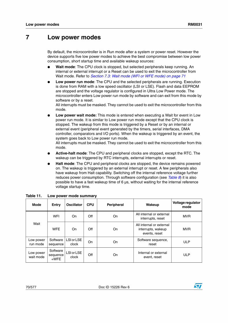
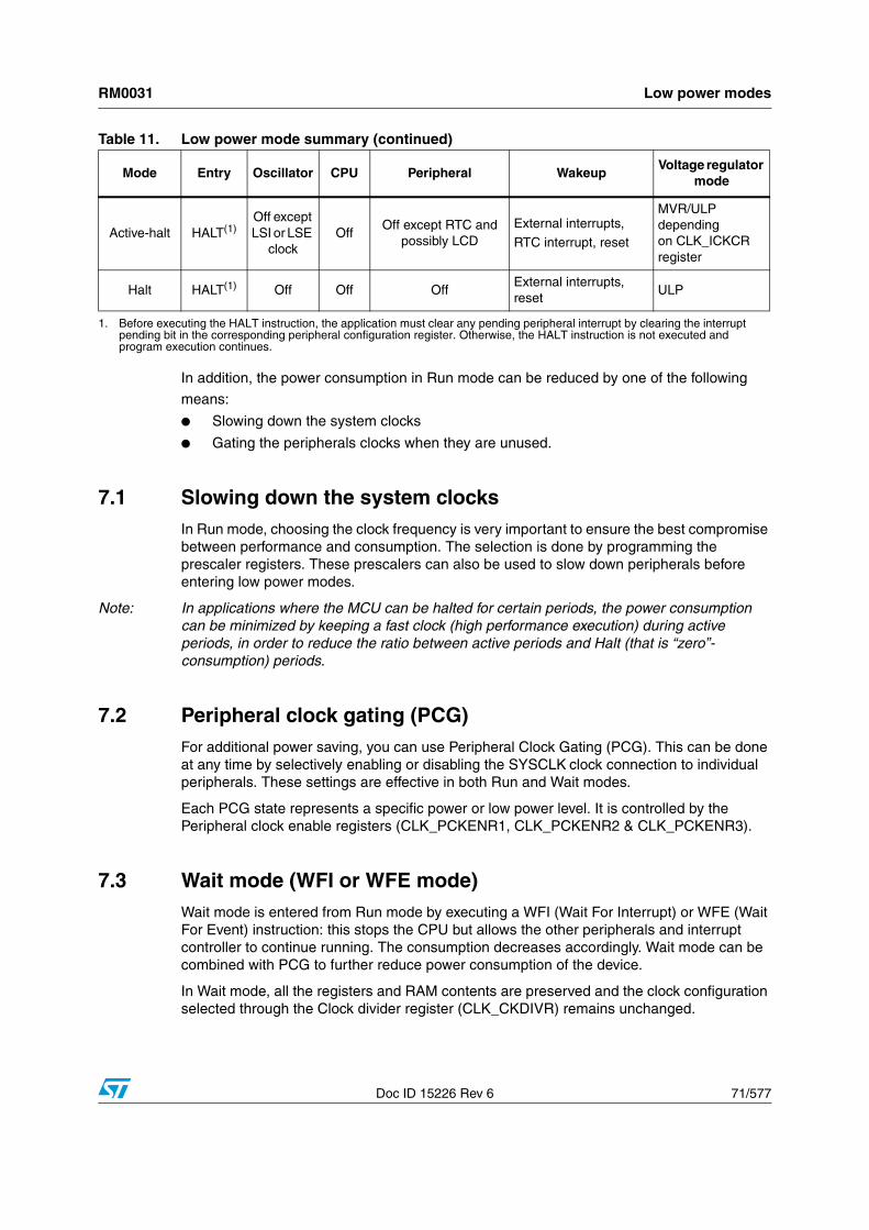
7 Low power modes
By default, the microcontroller is in Run mode after a system or power reset. However the device supports five low power modes to achieve the best compromise between low power consumption, short startup time and available wakeup sources:
● Wait mode: The CPU clock is stopped, but selected peripherals keep running. An internal or external interrupt or a Reset can be used to exit the microcontroller from Wait mode. Refer to Section 7.3: Wait mode (WFI or WFE mode) on page 71
● Low power run mode: The CPU and the selected peripherals are running. Execution is done from RAM with a low speed oscillator (LSI or LSE). Flash and data EEPROM are stopped and the voltage regulator is configured in Ultra Low Power mode. The microcontroller enters Low power run mode by software and can exit from this mode by software or by a reset. All interrupts must be masked. They cannot be used to exit the microcontroller from this mode.
● Low power wait mode: This mode is entered when executing a Wait for event in Low power run mode. It is similar to Low power run mode except that the CPU clock is stopped. The wakeup from this mode is triggered by a Reset or by an internal or external event (peripheral event generated by the timers, serial interfaces, DMA controller, comparators and I/O ports). When the wakeup is triggered by an event, the system goes back to Low power run mode. All interrupts must be masked. They cannot be used to exit the microcontroller from this mode.
● Active-halt mode: The CPU and peripheral clocks are stopped, except the RTC. The wakeup can be triggered by RTC interrupts, external interrupts or reset.
● Halt mode: The CPU and peripheral clocks are stopped, the device remains powered on. The wakeup is triggered by an external interrupt or reset. A few peripherals also have wakeup from Halt capability. Switching off the internal reference voltage further reduces power consumption. Through software configuration (see Table 8) it is also possible to have a fast wakeup time of 6 µs, without waiting for the internal reference voltage startup time.
Table 11. Low power mode summary
Mode Entry Oscillator CPU Peripheral WakeupVoltage regulator
mode
Wait
WFI On Off OnAll internal or external
interrupts, resetMVR
WFE On Off OnAll internal or external
interrupts, wakeup events, reset
MVR
Low power run mode
Software sequence
LSI or LSE clock
On OnSoftware sequence,
resetULP
Low power wait mode
Software sequence
+WFE
LSI or LSE clock
Off OnInternal or external
event, resetULP
RM0031 Low power modes
Doc ID 15226 Rev 6 71/577
In addition, the power consumption in Run mode can be reduced by one of the following
means:
● Slowing down the system clocks
● Gating the peripherals clocks when they are unused.
7.1 Slowing down the system clocksIn Run mode, choosing the clock frequency is very important to ensure the best compromise between performance and consumption. The selection is done by programming the prescaler registers. These prescalers can also be used to slow down peripherals before entering low power modes.
Note: In applications where the MCU can be halted for certain periods, the power consumption can be minimized by keeping a fast clock (high performance execution) during active periods, in order to reduce the ratio between active periods and Halt (that is “zero”- consumption) periods.
7.2 Peripheral clock gating (PCG)For additional power saving, you can use Peripheral Clock Gating (PCG). This can be done at any time by selectively enabling or disabling the SYSCLK clock connection to individual peripherals. These settings are effective in both Run and Wait modes.
Each PCG state represents a specific power or low power level. It is controlled by the Peripheral clock enable registers (CLK_PCKENR1, CLK_PCKENR2 & CLK_PCKENR3).
7.3 Wait mode (WFI or WFE mode)Wait mode is entered from Run mode by executing a WFI (Wait For Interrupt) or WFE (Wait For Event) instruction: this stops the CPU but allows the other peripherals and interrupt controller to continue running. The consumption decreases accordingly. Wait mode can be combined with PCG to further reduce power consumption of the device.
In Wait mode, all the registers and RAM contents are preserved and the clock configuration selected through the Clock divider register (CLK_CKDIVR) remains unchanged.
Active-halt HALT(1)Off except LSI or LSE
clockOff
Off except RTC and possibly LCD
External interrupts,
RTC interrupt, reset
MVR/ULP depending on CLK_ICKCR register
Halt HALT(1) Off Off OffExternal interrupts, reset
ULP
1. Before executing the HALT instruction, the application must clear any pending peripheral interrupt by clearing the interrupt pending bit in the corresponding peripheral configuration register. Otherwise, the HALT instruction is not executed and program execution continues.
Table 11. Low power mode summary (continued)
Mode Entry Oscillator CPU Peripheral WakeupVoltage regulator
mode
Low power modes RM0031
72/577 Doc ID 15226 Rev 6
7.4 Wait for interrupt (WFI) mode Wait for interrupt mode is entered from Run mode by executing a WFI (Wait For Interrupt) instruction.
When an internal or external interrupt request occurs, the CPU wakes up from WFI mode, serves the interrupt and resumes processing.
Note: In an interrupt based application, where most of the processing is done through the interrupt routines, the main program may be suspended by setting the activation level bit (AL) in the CFG_GCR register. Setting this bit causes the CPU to return to WFI mode without restoring the main execution context. This saves power by removing both the save/restore context activity and the need for a main software loop execution for power management (in order to return to WFI mode).
7.5 Wait for event (WFE) mode Wait for event mode is entered from Run mode by executing a WFE instruction.
Interrupt requests during this mode are served normally, depending on the value of the I0 and I1 bits in the CPU_CC register.
Peripheral events can be generated by the timers, serial interfaces, DMA controller, comparators and I/O ports. These are enabled by the WFE_CRx registers.
When a peripheral event is enabled, the corresponding interrupts are not served and you have to clear the corresponding flag status.
There are two ways to wake up the CPU from WFE mode:
● Interrupts: when an interrupt occurs, the CPU wakes up from WFE mode and serves the interrupt. After processing the interrupt, the processor goes back to WFE mode.
● Wakeup events: when a wakeup event occurs, the CPU wakes up and resumes processing. As the processing resumes directly after the WFE instruction, there is no context save/restore activity (this saves time and power consumption).
Further power consumption reduction may be achieved using this mode together with execution from RAM. In some very low power applications, when the main software routine is short and has a low execution time, this routine can be moved to RAM and executed from RAM. As the Flash program memory is not used at wakeup, the power consumption is then reduced during run time. At any time, another routine (stored in the Flash program memory) can be executed by software by simply calling/jumping to this routine.
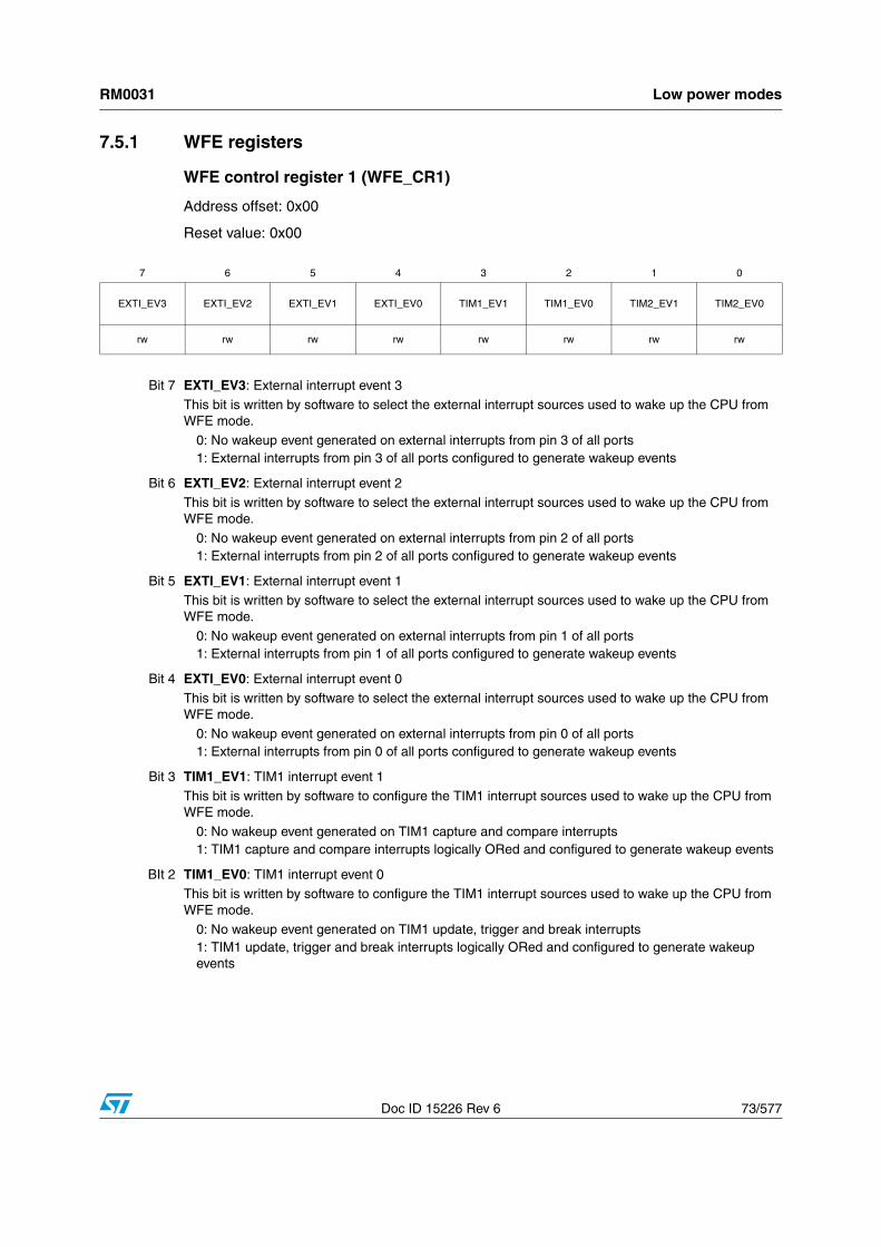
This bit is written by software to select the external interrupt sources used to wake up the CPU from WFE mode.
0: No wakeup event generated on external interrupts from pin 3 of all ports1: External interrupts from pin 3 of all ports configured to generate wakeup events
Bit 6 EXTI_EV2: External interrupt event 2
This bit is written by software to select the external interrupt sources used to wake up the CPU from WFE mode.
0: No wakeup event generated on external interrupts from pin 2 of all ports1: External interrupts from pin 2 of all ports configured to generate wakeup events
Bit 5 EXTI_EV1: External interrupt event 1
This bit is written by software to select the external interrupt sources used to wake up the CPU from WFE mode.
0: No wakeup event generated on external interrupts from pin 1 of all ports 1: External interrupts from pin 1 of all ports configured to generate wakeup events
Bit 4 EXTI_EV0: External interrupt event 0
This bit is written by software to select the external interrupt sources used to wake up the CPU from WFE mode.
0: No wakeup event generated on external interrupts from pin 0 of all ports1: External interrupts from pin 0 of all ports configured to generate wakeup events
Bit 3 TIM1_EV1: TIM1 interrupt event 1
This bit is written by software to configure the TIM1 interrupt sources used to wake up the CPU from WFE mode.
0: No wakeup event generated on TIM1 capture and compare interrupts1: TIM1 capture and compare interrupts logically ORed and configured to generate wakeup events
BIt 2 TIM1_EV0: TIM1 interrupt event 0
This bit is written by software to configure the TIM1 interrupt sources used to wake up the CPU from WFE mode.
0: No wakeup event generated on TIM1 update, trigger and break interrupts1: TIM1 update, trigger and break interrupts logically ORed and configured to generate wakeup events
Low power modes RM0031
74/577 Doc ID 15226 Rev 6
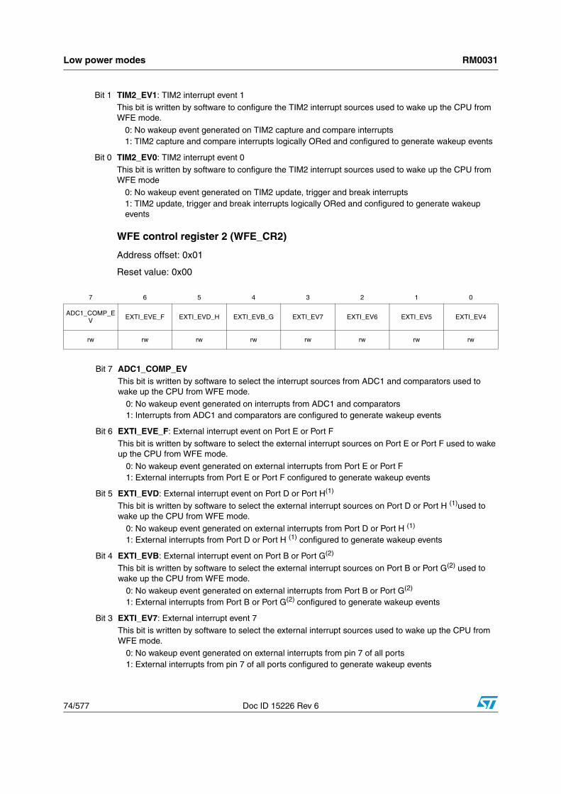
WFE control register 2 (WFE_CR2)
Address offset: 0x01
Reset value: 0x00
Bit 1 TIM2_EV1: TIM2 interrupt event 1This bit is written by software to configure the TIM2 interrupt sources used to wake up the CPU from WFE mode.
0: No wakeup event generated on TIM2 capture and compare interrupts1: TIM2 capture and compare interrupts logically ORed and configured to generate wakeup events
Bit 0 TIM2_EV0: TIM2 interrupt event 0This bit is written by software to configure the TIM2 interrupt sources used to wake up the CPU from WFE mode
0: No wakeup event generated on TIM2 update, trigger and break interrupts1: TIM2 update, trigger and break interrupts logically ORed and configured to generate wakeup events
Bit 7 ADC1_COMP_EVThis bit is written by software to select the interrupt sources from ADC1 and comparators used to wake up the CPU from WFE mode.
0: No wakeup event generated on interrupts from ADC1 and comparators 1: Interrupts from ADC1 and comparators are configured to generate wakeup events
Bit 6 EXTI_EVE_F: External interrupt event on Port E or Port F
This bit is written by software to select the external interrupt sources on Port E or Port F used to wake up the CPU from WFE mode.
0: No wakeup event generated on external interrupts from Port E or Port F1: External interrupts from Port E or Port F configured to generate wakeup events
Bit 5 EXTI_EVD: External interrupt event on Port D or Port H(1)
This bit is written by software to select the external interrupt sources on Port D or Port H (1)used to wake up the CPU from WFE mode.
0: No wakeup event generated on external interrupts from Port D or Port H (1)
1: External interrupts from Port D or Port H (1) configured to generate wakeup events
Bit 4 EXTI_EVB: External interrupt event on Port B or Port G(2)
This bit is written by software to select the external interrupt sources on Port B or Port G(2) used to wake up the CPU from WFE mode.
0: No wakeup event generated on external interrupts from Port B or Port G(2)
1: External interrupts from Port B or Port G(2) configured to generate wakeup events
Bit 3 EXTI_EV7: External interrupt event 7This bit is written by software to select the external interrupt sources used to wake up the CPU from WFE mode.
0: No wakeup event generated on external interrupts from pin 7 of all ports1: External interrupts from pin 7 of all ports configured to generate wakeup events
RM0031 Low power modes
Doc ID 15226 Rev 6 75/577
Bit 2 EXTI_EV6: External interrupt event 6This bit is written by software to select the external interrupt sources used to wake up the CPU from WFE mode.
0: No wakeup event generated on external interrupts from pin 6 of all ports1: External interrupts from pin 6 of all ports configured to generate wakeup events
Bit 1 EXTI_EV5: External interrupt event 5This bit is written by software to select the external interrupt sources used to wake up the CPU from WFE mode.
0: No wakeup event generated on external interrupts from pin 5 of all ports1: External interrupts from pin 5 of all ports configured to generate wakeup events
Bit 0 EXTI_EV4: External interrupt event 4This bit is written by software to select the external interrupt sources used to wake up the CPU from WFE mode.
0: No wakeup event generated on external interrupts from pin 4 of all ports1: External interrupts from pin 4 of all ports configured to generate wakeup events
1. External interrupt on port D for medium density devices and on port D or H for medium+ and high density devices.
2. External interrupt on port B for medium density devices and on port B or G for medium+ and high density devices.
Bit 7 DMA1CH23_EV: DMA1 channel 2 and 3 interrupt event
This bit is written by software to select the DMA1 channel 2 and 3 interrupt sources used to wake up the CPU from WFE mode.
0: No wakeup event generated on DMA1 channel 2 and 31: DMA1 channel 2 and 3 interrupts configured to generate wakeup events
Bit 6 DMA1CH01_EV: DMA1 channel 0 and 1 interrupt event
This bit is written by software to select the DMA1 channel 0 and 1 interrupt sources used to wake up the CPU from WFE mode.
0: No wakeup event generated on DMA1 channel 0 and 11: DMA1 channel 0and 1interrupts configured to generate wakeup events
Bit 5 USART1_EV: USART1 Rx and Tx interrupt event
This bit is written by software to select the USART1 Rx and Tx interrupt sources used to wake up the CPU from WFE mode
0: No wakeup event generated on USART1 Rx and Tx1: USART1 Rx and Tx interrupts configured to generate wakeup events
Bit 4 I2C1_EV: I2C1 Rx and Tx interrupt event
This bit is written by software to select the I2C1 Rx and Tx interrupt sources used to wake up the CPU from WFE mode
0: No wakeup event generated on I2C1 Rx and Tx1: I2C1 Rx and Tx interrupts configured to generate wakeup events
Bit 3 SPI1_EV: SPI1Rx and Tx interrupt event
This bit is written by software to select the SPI1Rx and Tx interrupt sources used to wake up the CPU from WFE mode
0: No wakeup event generated on SPI1Rx and Tx1: SPI1Rx and Tx interrupts configured to generate wakeup events
bit 2 TIM4_EV: TIM4 interrupt event
This bit is written by software to configure the TIM4 interrupt sources used to wake up the CPU from WFE mode
0: No wakeup event generated on TIM4 update and trigger interrupts1: TIM4 update and trigger interrupts logically ORed and configured to generate wakeup events
Bit 1 TIM3_EV1: TIM3 interrupt event 1
This bit is written by software to configure the TIM3 interrupt sources used to wake up the CPU from WFE mode.
0: No wakeup event generated on TIM3 capture and compare interrupts1: TIM3 capture and compare interrupts logically ORed and configured to generate wakeup events
RM0031 Low power modes
Doc ID 15226 Rev 6 77/577
Bit 0 TIM3_EV0: TIM3 interrupt event 0This bit is written by software to configure the TIM3 interrupt sources used to wake up the CPU from WFE mode.
0: No wakeup event generated on TIM3 update, trigger and break interrupts1: TIM3 update, trigger and break interrupts logically ORed and configured to generate wakeup events
This bit is written by software to configure the AES interrupt source used to wake up the CPU from WFE mode.
0: No wakeup event generated from AES peripheral1: AES interrupt configured to generate wakeup event
Bit 5 TIM5_EV1: TIM5 interrupt event 1
This bit is written by software to configure the TIM5 interrupt sources used to wake up the CPU from WFE mode.
0: No wakeup event generated on TIM5 capture and compare interrupts1: TIM5 capture and compare interrupts logically ORed and configured to generate wakeup events
Bit 4 TIM5_EV0: TIM5 interrupt event 0
This bit is written by software to configure the TIM5 interrupt sources used to wake up the CPU from WFE mode.
0: No wakeup event generated on TIM5 update, trigger and break interrupts1: TIM5 update, trigger and break interrupts logically ORed and configured to generate wakeup events
Bit 3 USART3_EV: USART3 Rx and Tx interrupt event0: No wakeup event generated from USART3 Rx and Tx1: USART3 Rx and Tx interrupts configured to generate wakeup events
Bit 2 USART2_EV: USART2 Rx and Tx interrupt eventThis bit is written by software to select the USART2 Rx and Tx interrupt sources used to wake up the CPU from WFE mode
0: No wakeup event generated from USART2 Rx and Tx1: USART2 Rx and Tx interrupts configured to generate wakeup events
Bit 1 SPI2_EV: SPI2 Rx and Tx interrupt event
This bit is written by software to select the SPI2 Rx and Tx interrupt sources used to wake up the CPU from WFE mode.
0: No wakeup event generated from SPI2 Rx and Tx1: SPI2 Rx and Tx interrupts configured to generate wakeup events
Bit 0 RTC_CSSLSE_EV: “RTC” or “CSS on LSE” interrupt event
This bit is written by software to select the interrupt source (“RTC” or “CSS on LSE”) used to wake up the CPU from WFE mode.
0: No wakeup event generated from RTC or CSS on LSE interrupt events1: RTC or CSS on LSE interrupt events configured to generate wakeup events
RM0031 Low power modes
Doc ID 15226 Rev 6 79/577
7.5.2 WFE register map and reset values
Table 12. WFE register map
Address
offset(1)Register
name7 6 5 4 3 2 1 0
0x00WFE_CR1Reset value
EXTI_EV30
EXTI_EV20
EXTI_EV10
EXTI_EV00
TIM1_EV10
TIM1_EV00
TIM2_EV10
TIM2_EV00
0x01WFE_CR2Reset value
ADC1_COMP_EV
0
EXTI_EVE_F0
EXTI_EVD0
EXTI_EVB0
EXTI_EV70
EXTI_EV60
EXTI_EV50
EXTI_EV40
0x02WFE_CR3Reset value
DMA1CH23_EV
0
DMA1CH01_EV
0
USART1_EV0
I2C1_EV
0
SPI1_EV
0
TIM4_EV
0
TIM3_EV1
0
TIM3_EV0
0
0x03(2) WFE_CR4Reset value
Reserved AES_EV0
TIM5_EV10
TIM5_EV00
USART3_EV0
USART2_EV 0
SPI2_EV 0
RTC_CSSLSE_EV0
1. Please refer to the “general hardware register map” table in the datasheet for details on register addresses.
2. Available on medium+ and high density devices only.
Low power modes RM0031
80/577 Doc ID 15226 Rev 6
7.6 Low power run modeThis mode is based on code fetch from RAM with the regulator in Ultralow power mode (ULP) and EEPROM in IDDQ.
While using this mode you have to switch from high speed clock sources to low speed clock sources.
Note: The ADC cannot be used in Low Power Run mode and must be disabled.
7.6.1 Entering Low power run mode
This mode is entered by executing the following software sequence:
1. Jump to RAM
2. Switch system clock to LSI or LSE clock sources
3. Switch off the high speed oscillators, the ADC and all unused peripherals
4. Mask all interrupts
5. Switch off the Flash/Data EEPROM by setting EEPM bit in FLASH_CR1 register
6. Add a software delay loop to ensure Flash/Data EEPROM off status
7. Configure the ultralow power mode for the regulator by setting the REGOFF bit in the CLK_REGCSR register
7.6.2 Exiting Low power run mode
The only way to exit this mode is to follow these steps:
1. Switch on the main regulator by resetting the REGOFF bit in the CLK_REGCSR register. The REGREADY flag in the CLK_REGCSR register is set when the regulator is ready.
2. Switch on the Flash/Data EEPROM by resetting EEPM bit in FLASH_CR1 register. The EEREADY flag in the CLK_REGCSR register is set when the Flash/Data EEPROM is ready.
3. Reset interrupt mask.
4. Switch on what is necessary and jump to Flash/Data EEPROM if needed.
7.7 Low power wait mode This mode is entered by executing a WFE instruction when the MCU is in Low power run mode. It can be exited only by means of an external or internal event. In this case the MCU returns to Low power run mode.
RM0031 Low power modes
Doc ID 15226 Rev 6 81/577
7.8 Halt modeIn this mode the system clock is stopped. This means that the CPU and all the peripherals clocked by SYSCLK or by derived clocks are disabled, except for the following cases:
● The HSI clock is not stopped if used by SWIM
● The system clock source is not stopped if a Flash/Data EEPROM write operation is in progress
● The LSI clock is not stopped if used by the SWIM, the IWDG or if the “IWDG_HALT” option bit is disabled.
In Halt mode, none of the peripherals are clocked and the digital part of the MCU consumes almost no power.
7.8.1 Entering Halt mode
The MCU enters Halt mode when a HALT instruction is executed.
Note: It is recommended not to enter Halt/Active-halt mode from the Low power run mode. Otherwise, the only safe way to exit one of these two modes is to reset the MCU.
Before executing a HALT instruction, the application must clear all pending peripheral interrupts by clearing the interrupt pending bit in the corresponding peripheral configuration register. Otherwise, the HALT instruction is not executed and program execution continues.
However, the Halt procedure can be delayed if one of the following flags is set:
● SWBSY flag in the CLK_SWCR register
● EEBUSY flag in the CLK_CLK_REGCSR register
● RTCSWBSY flag in the CLK_CRTCR register
● BEEPSWBSY flag in the CLK_CBEEPR register when BEEP in Active-halt mode enabled.
If SAHALT bit is set in the CLK_ICKCR register the main regulator (MVR) will be switched off without taking into account that some high-speed clock may be used by the system.
7.8.2 Exiting Halt mode
Wakeup from Halt mode is triggered by an external interrupt sourced by a general purpose I/O port configured as interrupt input or by an alternate function pin capable of triggering a peripheral interrupt.
The system clock is restarted with a frequency depending on the FHW bit in the CLK_ICKCR register. If the FHW bit is set, HSI/8 is the system clock, otherwise the system clock is the last selected clock source before entering Halt mode.
In an interrupt based application, where most of the processing is done through the interrupt routines, the main program may be suspended by setting the activation level bit (AL) in the CPU configuration register. Setting this bit causes the CPU to return to Halt mode when executing the return from interrupt, without restoring the main execution context.
Power consumption is reduced as there is no save/restore context activity and no need for a main software loop execution for power management (in order to return to WFI mode).
After a wake up from Halt mode, the LCD clock switches from RTCCLK to SYSCLK. To have a stable clock signal without glitches, 2 RTCCLK cycles are needed for synchronization
Low power modes RM0031
82/577 Doc ID 15226 Rev 6
reasons. Consequently, read/write access to LCD registers is not possible during this period.
7.9 Active-halt modeActive-halt mode is similar to Halt mode.
Note: It is recommended not to enter Halt/Active-Halt mode from the Low power run mode. Otherwise, the only safe way to exit one of these two modes is to reset the MCU.
In Active-halt mode, the main oscillator, the CPU and almost all peripherals are stopped.Only oscillator or the LSE crystal is running to drive the SWIM, beeper, IWDG, RTC and LCD if enabled.
RM0031 Reset (RST)
Doc ID 15226 Rev 6 83/577
8 Reset (RST)
There are 6 reset sources:
● External reset through the NRST pin (this pin can also be configured as general purpose output)
● Power-on reset (POR)/ power-down reset (PDR)
● Independent watchdog reset (IWDG)
● Window watchdog reset (WWDG)
● Illegal opcode reset (ILLOP)
● SWIM reset
These sources act on the NRST pin. The reset service routine vector is fixed at address 0x8000 in the memory map.
Figure 13. Reset circuit
8.1 “Reset state” and “under reset” definitionsWhen a reset occurs, there is a reset phase from the external pin pull-down to the internal reset signal release. During this phase, the microcontroller sets some hardware configurations before going to the reset vector.
At the end of this phase, most of the registers are configured with their “reset state” values. During the reset phase, i.e. “under reset”, some pin configurations may be different from their “reset state” configuration.
8.2 External reset (NRST pin)
8.2.1 Asynchronous external reset description
The NRST pin is both an input and an open-drain output with an integrated RPU weak pull-up resistor.
A low pulse of minimum 300 ns on the NRST pin is needed to generate an external reset. The reset detection is asynchronous and therefore the MCU can enter reset even in Halt mode.
NRST
RPU
VDD
WWDG resetIWDG resetPulse
generator SWIM reset
Externalreset
(min 20 µs)
System resetFilter
Illegal opcode resetBOR/PDR
ai17040c
Reset (RST) RM0031
84/577 Doc ID 15226 Rev 6
The NRST pin also acts as an open-drain output for resetting external devices.
Any reset pulse from an internal reset source holds the NRST output low for at least 20 µs. The internal RPU weak pull-up ensures a high level on the NRST pin when the reset is not forced low.
8.2.2 Configuring NRST/PA1 pin as general purpose output
To optimize the number of available pins, the NRST pin (external reset) can be configured as a general purpose push-pull output (PA1).
For security, this configuration can be performed once only after reset, by writing a specified key (0xD0) to the Reset pin configuration register (RST_CR).
When the PA1 pin is configured as a general purpose output, the MCU can be reset only by a power-on reset (POR) or other internal reset source.
8.3 Internal resetFor internal reset sources, the NRST pin is kept low during the delay phase generated by the pulse generator.
Each internal reset source is linked to a specific flag bit in the Reset status register (RST_SR). These flags are set at reset state depending on the given reset source. Consequently, they can be used to identify the last reset source. They are cleared by software by writing the logic value ‘1’.
Note: All flags besides the POR flag are reset at POR.
8.3.1 Power-on reset (POR)
During power-on, the POR keeps the device in reset mode until VDD reaches a specified threshold. The POR reset is then held for a specified time to ensure that VDD has reached the minimum operating voltage.See Electrical parameters section in the datasheet for more details.
8.3.2 Independent watchdog reset
Refer to the independent watchdog chapter for details.
A reset can be triggered by the application software using the Independent watchdog.
8.3.3 Window watchdog reset
Refer to the window watchdog chapter for details.
8.3.4 SWIM reset
An external device connected to the SWIM interface can request the SWIM block to generate an MCU reset.
8.3.5 Illegal opcode reset
A system of illegal opcode detection is implemented to enhance device robustness against unexpected behaviors. If the code to be executed does not correspond to any opcode or
RM0031 Reset (RST)
Doc ID 15226 Rev 6 85/577
prebyte value, a reset is generated. This, combined with the Watchdog, allows recovery from an unexpected fault or interference.
Reset (RST) RM0031
86/577 Doc ID 15226 Rev 6
8.4 RST registers
8.4.1 Reset pin configuration register (RST_CR)
Address offset: 0x00
Reset value: 0x00
8.4.2 Reset status register (RST_SR)
Address offset: 0x01
Reset value after power-on Reset: 0x01
7 6 5 4 3 2 1 0
RSTPIN_KEY
rwo rwo rwo rwo rwo rwo rwo rwo
Bits 7:0 RSTPIN_KEY[7:0]: Reset pin configuration key0x00: NRST/PA1 configured as reset pin (default reset value)0xD0: NRST/PA1 configured as general purpose output
These bits are write once only. They can also be read at any time.
Note: Writing any value beside 0xD0 is equivalent to writing 0x00.
7 6 5 4 3 2 1 0
ReservedBORF WWDGF SWIMF ILLOPF IWDGF PORF
rc_w1 rc_w1 rc_w1 rc_w1 rc_w1 rc_w1
Bits 7:6 Reserved, must be kept cleared.
Bit 5 BORF: Brownout reset flag
This bit is set by hardware and cleared by software writing “1”.
0: No BOR reset occurred1: An BOR reset occurred
Bit 4 WWDGF: Window Watchdog reset flag
This bit is set by hardware and cleared by software writing “1”.0: No WWDG reset occurred1: A WWDG reset occurred
Bit 3 SWIMF: SWIM reset flagThis bit is set by hardware and cleared by software writing “1”.
0: No SWIM reset occurred1: A SWIM reset occurred
Bit 2 ILLOPF: Illegal opcode reset flag
This bit is set by hardware and cleared by software writing “1”.
0: No ILLOP reset occurred1: An ILLOP reset occurred
Bit 1 IWDGF: Independent Watchdog reset flag
This bit is set by hardware and cleared by software writing “1”.0: No IWDG reset occurred1: An IWDG reset occurred
RM0031 Reset (RST)
Doc ID 15226 Rev 6 87/577
8.4.3 RST register map and reset values
Bit 0 PORF: Power-on Reset (POR) flag This bit is set by hardware and cleared by software writing “1”.
0: No POR occurred1: A POR occurred
Table 13. RST register map and reset values
Address offset(1)
1. Please refer to the “general hardware register map” table in the datasheet for details on register addresses.
Register name 7 6 5 4 3 2 1 0
0x00RST_CR
Reset value
RSTPIN_KEY7
0
RSTPIN_KEY6
0
RSTPIN_KEY5
0
RSTPIN_KEY4
0
RSTPIN_KEY3
0
RSTPIN_KEY2
0
RSTPIN_KEY1
0
RSTPIN_KEY0
0
0x01RST_SR
Reset value-0
-0
BORF0
WWDGF0
SWIMF0
ILLOPF0
IWDGF0
PORF1
Clock control (CLK) RM0031
88/577 Doc ID 15226 Rev 6
9 Clock control (CLK)
This section applies to medium density STM8L15x devices, medium+ density STM8L15x devices and high density STM8L15x/STM8L16x devices, unless otherwise specified.
9.1 IntroductionThe clock controller is designed to be very robust and at the same time easy to use. Its purpose is to obtain the best performance in the application while at the safme time get the full benefit of all the microcontroller power saving capabilities.
You can manage the clock distribution to the CPU and to the various peripherals, in order to optimize the power consumption.
A safe and glitch-free switch mechanism allows you to switch the system clock division factor on the fly, by means of clock prescaler.
Figure 14. Clock structure
1. The HSE clock source can be either an external crystal/ceramic resonator or an external source (HSE bypass). Refer to Section 9.2: HSE clock.
2. The LSE clock source can be either an external crystal/ceramic resonator or a external source (LSE bypass). Refer to Section 9.4: LSE clock.
3. 14 bits in medium density devices and 20 bits in medium+ and high density devices.
4. Available on medium+ and high density devices only.
Four different clock sources can be used to drive the system clock:
Each clock source can be switched on or off independently when it is not used, to optimize power consumption.
These four clocks can be used with a programmable prescaler (factor 1 to 128) to drive the system clock (SYSCLK). The SYSCLK is used to clock the core, memory and peripherals. After reset, the device restarts by default with the HSI clock divided by 8. The prescaler ratio and clock source can be changed by the application program as soon as the code execution starts.
All the peripheral clocks are derived from the system clock (SYSCLK) except:
● The BEEP clock which is derived from the LSE or LSI clocks. This selection is made by programming the CLKBEEPSEL[1:0] bits in the Clock BEEP register (CLK_CBEEPR).
● The RTC and the LCD clock which is derived from the LSE, LSI HSI or HSE (HSI and HSE are divided by a programmable prescaler in CLK_CRTCR register). For more information about the RTC and LCD clock source configuration please refer to Section 9.9: RTC and LCD clock
● The IWDG clock which is always the LSI clock.
9.2 HSE clock The high-speed external clock signal (HSE) can be generated from two possible clock sources:
● HSE external crystal/ceramic resonator
● HSE user external clock
Note: The resonator and the load capacitors have to be placed as close as possible to the oscillator pins in order to minimize output distortion and start-up stabilization time. The loading capacitance values must be adjusted according to the selected oscillator.
Clock control (CLK) RM0031
90/577 Doc ID 15226 Rev 6
External crystal/ceramic resonator (HSE crystal)
The 1 to 16 MHz external oscillator has the advantage of producing a very accurate rate on the main clock with 50% duty cycle.
The associated hardware configuration is shown in Figure 15. Refer to the electrical characteristics section in the product datasheet for more details.
At start up the clock signal produced by the oscillator is not stable, and by default a delay of 1 oscillator cycle is inserted before the clock signal is released. You can program another stabilization time in the HSECNT option byte, please refer to option bytes section in the datasheet.
The HSERDY flag in the External clock register (CLK_ECKCR) indicates if the high-speed external oscillator is stable or not. At startup, the clock is not released until this bit is set by hardware.
The HSE crystal can be switched on and off using the HSEON bit in the External clock register (CLK_ECKCR).
External source (HSE bypass)
In this mode, an external clock source must be provided. It can have a frequency up to 16 MHz. The application can select this mode by setting the HSEBYP and HSEON bits in the External clock register CLK_ECKCR. The external clock signal (square, sinus or triangle) with ~50% duty cycle has to drive the OSC_IN pin while the OSC_OUT pin is available as standard I/O. See Figure 15.
Note: Before selecting this mode, you have to make sure that the HSE clock source is not used by the RTC, output or involved in a switching operation.
Figure 15. HSE clock sources
Hardware configuration
Ext
ern
alcl
ock
Cry
stal
/cer
amic
reso
nat
ors
OSC_OUT
EXTERNALSOURCE
(I/O available)
OSC_IN OSC_OUT
LOADCAPACITORS
CL2CL1
RM0031 Clock control (CLK)
Doc ID 15226 Rev 6 91/577
9.3 HSI clockThe HSI clock signal is generated from an internal 16 MHz RC.
At startup the system clock source is automatically selected as HSI RC clock output divided by 8 (HSI/8).
The HSI RC oscillator has the advantage of providing a 16-MHz system clock source with 50% duty cycle at low cost (no external components). It also has a faster startup time than the HSE crystal oscillator however, even with calibration the frequency is less accurate than an external crystal oscillator or ceramic resonator.
Calibration
Each device is factory-calibrated. After reset, the factory calibration value is automatically loaded in the HSI calibration register (CLK_HSICALR)) and used for trimming the HSI oscillator. The read only content of the CLK_HSICALR register can be used as a reference for a calibration by the user.
If the application is subject to voltage or temperature variations, this may affect the RC oscillator speed. You can trim the HSI frequency in the application using the HSI clock calibration trimming register (CLK_HSITRIMR). This register provides the internal HSI calibration register value.
Before writing to this register, you have to unlock the hardware write protection and then use the following procedure:
1. Two consecutive write accesses to HSI unlock register (CLK_HSIUNLCKR), the first one with the value 0xAC and the second one with the value 0x35.
2. Write the HSI trimming value to the HSI clock calibration trimming register (CLK_HSITRIMR).
When this procedure is properly completed, the CLK_HSITRIMR is locked again and the written HSI trimming value is the calibration value used to trim the HSI oscillator.
Backup source
The HSI clock can also be used as a backup source (auxiliary clock) if the HSE crystal oscillator fails. Refer to Section 9.8: Clock security system (CSS) on page 96.
Fast wakeup feature
If the FHWU bit in the Internal clock register (CLK_ICKCR) is set, this automatically selects the HSI clock as system clock after the MCU wakeup from Halt or Active-halt mode. Otherwise, the same clock source as that used before entering Halt or Active-halt mode is selected.
9.4 LSE clockThe LSE crystal is a 32.768 kHz low speed external crystal or ceramic resonator. It has the advantage of providing a low power and highly accurate clock source to the real-time clock peripheral (RTC) for clock/calendar or other timing functions.
The LSE crystal is switched on and off using the LSEON bit in the external clock register (CLK_ECKCR). It is also automatically switched on when it is selected as RTC, CCO, Beep or system clock source. At startup, the LSE crystal output clock signal is transmitted to the
Clock control (CLK) RM0031
92/577 Doc ID 15226 Rev 6
MCU after the LSERDY flag has been set by hardware in the external clock register (CLK_ECKCR).
Note: It is forbidden to enable CCO before the end of the LSE startup time tSU(LSE).
It is also recommended to wait for this LSE startup time before enabling other features using the LSE, in order to have a stabilized frequency.
External source (LSE bypass)
In this mode, an external clock source must be provided. It must have a frequency of 32.768 kHz. The application can select this mode by setting the LSEBYP and LSEON bits in the External clock register (CLK_ECKCR). The external clock signal (square, sinus or triangle) with ~50% duty cycle has to drive the OSC32_IN pin while the OSC32_OUT pin is available as standard I/O. See Figure 15.
Note: Before selecting this mode, you have to make sure that the LSE clock source is not used by the RTC output or involved in a switching operation.
9.5 LSI clockThe LSI RC acts as a low power clock source that can be kept running in Active-halt and Run modes for the independent watchdog (IWDG). The clock frequency is around 38 kHz. For more details, refer to the electrical characteristics section in the product datasheet.
The LSI RC can be switched on and off using the LSION bit in the internal clock register (CLK_ICKCR).
To detect a sequence of entry into SWIM mode, the LSI is automatically kept enabled in all modes except Halt and Active-halt modes. Consequently, the LSI can be switched off by clearing the LSION bit only if no peripheral is clocked by the LSI and after SWIM has been disabled by setting the SWD bit in the CFG_GCR register. The LSI is not kept ON by the SWIM in Halt and Active-halt mode.
The LSIRDY flag in the Internal clock register (CLK_ICKCR) indicates if the low-speed internal oscillator is stable or not. At startup, the clock is not released until this bit is set by hardware.
9.6 System clock sources
9.6.1 System startup
For fast system startup, after a reset the clock controller configures the system clock source as HSI RC clock output divided by 8 (HSI/8). This is to take advantage of the short stabilization time of the HSI oscillator.
Once the system clock is released, the user program can switch the system clock to another clock source (LSI, HSE, or LSE) and/or modify the prescaler ratio.
9.6.2 System clock switching procedures
The clock switching feature provides an easy to use, fast and secure way for the application to switch from one system clock source to another.
RM0031 Clock control (CLK)
Doc ID 15226 Rev 6 93/577
To switch clock sources, you can proceed in one of two ways:
● Automatic switching
● Manual switching
Automatic switching
The automatic switching enables the user to launch a clock switch with a minimum number of instructions. The software can continue doing other operations without taking care of the switch event exact time.
Refer to the flowchart in Figure 16.
Use the following procedure:
1. Enable the switching mechanism by setting the SWEN bit in the Switch control register (CLK_SWCR).
2. Write the 8-bit value used to select the target clock source in the System clock switch register (CLK_SWR). The SWBSY bit in the CLK_SWCR register is set by hardware, and the target source oscillator starts. The old clock source continues to drive the CPU and peripherals.
As soon as the target clock source is ready (stabilized), the content of the CLK_SWR register is copied to the System clock status register (CLK_SCSR).
The SWBSY bit is cleared and the new clock source replaces the old one. If the SWIEN bit is set, the SWIF flag in the CLK_SWCR is set and an interrupt is generated.
Manual switching
The manual switching is not as immediate as the automatic switching but it offers to the user a precise control of the switch event time.
Refer to the flowchart in Figure 17.
1. Write the 8-bit value used to select the target clock source in the System clock switch register (CLK_SWR). Then the SWBSY bit is set by hardware, and the target source oscillator starts. The old clock source continues to drive the CPU and peripherals.
2. The software has to wait until the target clock source is ready (stabilized). This is indicated by the SWIF flag in the CLK_SWCR register and by an interrupt if the SWIEN bit is set.
3. The final software action is to set, at the chosen time, the SWEN bit in the CLK_SWCR register to execute the switch.
In both manual and automatic switching modes, the old system clock source will not be powered off automatically in case it is required by other blocks (the LSI RC may be used to drive the independent watchdog for example). The clock source can be powered off using the bits in the Internal clock register (CLK_ICKCR) and the external clock register (CLK_ECKCR).
If the clock switch does not work for any reason, software can reset the current switch oper-
ation by clearing the SWBSY flag. This will restore the CLK_SWR register to its previous
content (old system clock).
Note: After having reset a clock master switch procedure by clearing the SWBSY flag, the application must wait until a period of at least two clock cycles has elapsed before generating any new clock master switch request.
9.7 Peripheral clock gating (PCG)Peripheral clock Gating (PCG) mode selectively enables or disables the system clock (SYSCLK) connection to peripherals at any time in run or slow mode to optimize power consumption.
After a device reset, all peripheral clocks are disabled. The only bit which is enabled by default at reset state is PCKEN27 as it is used for the BootROM. Software has to be properly written to switch off the ROM clock after the Bootloader execution.
You can enable the clock to any peripheral by setting the corresponding PCKEN bit in the CLK_PCKENRx peripheral clock gating registers.
● To enable a peripheral, first enable the corresponding PCKEN bit in the CLK_PCKENR registers and then set the peripheral enable bit in the peripheral control registers.
● To disable properly the peripheral, first disable the appropriate bit in the peripheral control registers and then stop the corresponding clock.
Note: The beeper, RTC and LCD are fed by a specific clock different from SYSCLK, so that they continue to run even if the clock gating to the peripheral registers is asserted.
Reset
MCU in Run mode with HSI/8
Write target clock source in CLK_SWR
Target clock source ready after
CLK_SWR CLK_SCSR
SWBSY 0
Target clock source powered on
SWBSY 1
stabilization time
Switch busy
MCU in Run modewith new system clock source
SOFTWARE ACTIONHARDWARE ACTION
Reset Switch busy flag
Update system clock status
Clear SWIF flag
Set SWIEN bit in CLK_SWCR to enable interrupt if suitable
Set SWEN bit in CLK_SWCR to execute switch
Interrupt if activated
Ready for the switchPoll the target clock
LSIRDY/LSERDY/HSERDY/HSIRDY
Clock control (CLK) RM0031
96/577 Doc ID 15226 Rev 6
9.8 Clock security system (CSS)
9.8.1 Clock security system on HSE
The clock security system (CSS) monitors HSE crystal clock source failures when HSE is used as the system clock. If the HSE clock fails due to a broken or disconnected resonator or any other reason, the clock controller activates a stall-safe recovery mechanism by automatically switching SYSCLK to the HSI with the same division factor as that used before the HSE clock failure. Once selected, the auxiliary clock source remains enabled until the microcontroller is reset. The application can enable the clock security system by setting the CSSEN bit in the Clock security system register (CLK_CSSR). For safety reason, once CSS is enabled it cannot be disabled until the next device reset.
The following conditions must be met to detect HSE quartz crystal failures through the CSS:
● HSE on and stabilized (HSEON=1 and HSERDY=1 in the External clock register (CLK_ECKCR)
● CSS function enabled (CSSEN=1 in the Clock security system register (CLK_CSSR))
If HSE is the current system clock when a failure is detected, the CSS performs the following actions:
● The HSI is switched on (if it was off) (HSION bit in Internal clock register (CLK_ICKCR) register is set).
● The HSE is switched off (HSEON bit in the CLK_ECKCR register is reset)
● The AUX bit is set to indicate that the HSI is used as system clock source. The division factor of the system clock is not modified.
● All CLK registers are write protected except the System clock divider register (CLK_CKDIVR). The application can still change the system clock prescaler.
● The CSSD bit is set in the CLK_CSSR register and an interrupt is generated if the CSSDIE bit is set.
Note: CSSD and AUX flags are cleared only by device reset.
If HSE is not the current system clock source when a failure is detected, the CSS performs the following actions:
● The HSE is switched off (HSEON bit in the CLK_ECKCR is reset)
● The CSSD bit is set in the CLK_CSSR register and an interrupt is generated if the CSSDIE bit is set.
When the CSSDIE bit is set, if the HSE clock fails, the CSS interrupt is triggered and is executed indefinitely until the CSS interrupt enable bit is cleared. As a consequence, the application must clear the CSSDIE bit in CLK_CSSR register in the CLK interrupt service routine (ISR).
When the HSE is selected as system clock source, if the HSE fails before reaching the required stabilization time, it is not detected (CSSD equal to zero) and the system clock remains fed by the previous clock. In this case, the application must abort the clock switching procedure by clearing the SWBSY bit in the Switch control register (CLK_SWCR).
RM0031 Clock control (CLK)
Doc ID 15226 Rev 6 97/577
9.8.2 Clock security system on LSE
A second clock security system is implemented on medium+ and high density devices to monitor LSE crystal clock source failures when LSE is used as RTC clock. The LSE failure detection is made through the LSI oscillator.
This feature is implemented externally to the RTC peripheral and has no impact on clock controller registers. To work properly, it requires an LSE clock frequency greater than LSI/4.
Depending on the configuration of the SWITCHEN bit in the CSSLSE_CSR register, the RTC clock can be automatically switched from LSE to LSI when a LSE failure is detected.
The application can enable the clock security system on LSE and switch to LSI by setting respectively the CSSEN bit and the SWITCHEN bit in the CSSLSE_CSR register.
For safety reason, once the CSS on LSE is enabled, it cannot be disabled until the next power-on reset.
The following conditions must be met to detect LSE quartz crystal failures through the CSS on LSE when LSE is used as RTC clock source:
● Enable the peripheral clock by setting the CSS_LSE bit in the CLK_PCKENR3 register
● Enable the LSI clock by setting the LSION bit in the CLK_ICKCR register
● Configure the LSE as RTC clock source through the CLK_CRTCR register.
Note: If the CSS on LSE is enabled without configuring the LSE as RTC clock source, a false failure will be detected, due to the fact that the RTC clock is missing.
● Enable the CSS on LSE by setting the CSSEN bit in the CSSLSE_CSR register
Note: Before enabling the CSS on LSE, the user must wait until the LSE startup time tSU(LSE) has elapsed
● If needed, enable the automatic clock switch from LSE to LSI on LSE failures by setting the SWITCHEN bit in the CSSLSE_CSR register.
● When an LSE failure is detected:
– The CSSF bit is set in the CSSLSE_CSR register and an interrupt is generated if the CSSIE bit is set.
– If the SWITCHEN bit is set : the RTC clock source is switched to LSI and the SWITCHF bit is set in the CSSLSE_CSR register. The RTC clock source remains the LSI until the next power-on reset. The CLK_CRTCR register is not updated by the switch and cannot control the RTC clock until the next power-on.
Note: The RTC clock source is the LSI clock instead of the LSE clock when the SWITCHF bit is set.
– If the SWITCHEN bit is reset: the RTC clock source remains the LSE clock.
CSS on LSE low power modes
The following table describes the behavior of the CSS on LSE in low power modes.
Table 14. CSS on LSE in low power modes
Mode Description
Halt/ Active-haltCSSF interrupts cause the device to exit from Active-halt or Halt mode
Clock control (CLK) RM0031
98/577 Doc ID 15226 Rev 6
9.7.1.2 CSS on LSE control and status register (CSSLSE_CSR)
Address offset: 0x00
Power-on reset value: 0x00Reset value: 0xXX (the registers are not impacted by a system reset. They are reset at power-on).
9.8.3 CSS on LSE register map and reset values
7 6 5 4 3 2 1 0
Reserved SWITCHF CSSF CSSIE SWITCHEN CSSEN
r r rw rw rwo rwo
Bits 7:5 Reserved, must be kept cleared.
Bit 4 SWITCHF: RTC clock switch flag
This bit is set by hardware and only cleared by device reset.0: No RTC clock switch occurred or no failure on LSE detected1: RTC clock switch to LSI completed
Bit 3 CSSF: CSS on LSE flagThis bit is set by hardware and cleared by software by writing 0.
0: CSS on LSE is OFF or no LSE crystal clock disturbance is detected.
1: An LSE crystal clock disturbance is detected.
Bit 2 CSSIE: Clock security system on LSE interrupt enable
This bit is set and cleared by software.0: Clock security system on LSE interrupt disabled1: Clock security system on LSE interrupt enabled
Bit 1 SWITCHEN: RTC clock switch to LSI in case of LSE failure enable This bit is set only by software and can be cleared only by device reset.
0: Clock switch to LSI in case of LSE failure OFF1: Clock switch to LSI in case of LSE failure ON
Bit 0 CSSEN: Clock security system on LSE enable
This bit is set only by software and can be cleared only by device reset.
0: Clock security system on LSE OFF1: Clock security system on LSE ON
Table 15. CSS on LSE register map
Address
offset(1)Register
name7 6 5 4 3 2 1 0
0x00CSSLSE_CSRPower-on reset
value
-0
-0
-0
SWITCHF0
CSSF0
CSSIE0
SWITCHEN0
CSSEN0
1. Please refer to the “general hardware register map” table in the datasheet for details on register addresses.
RM0031 Clock control (CLK)
Doc ID 15226 Rev 6 99/577
9.9 RTC and LCD clockThe RTC has two clock sources:
● RTCCLK used for RTC timer/counter
RTCCLK can be either the HSE, LSE, HSI or LSI clock. This selection is performed by programming the RTCSEL[3:0] bits in the Clock RTC register (CLK_CRTCR). These clocks can be optionally divided by a programmable divider (factor 1 to 64) by programming the RTCDIV[2:0] bits in the Clock RTC register (CLK_CRTCR). When the HSE or HSI clock is selected as RTCCLK source, this clock must be divided to have a maximum of 1 MHz as input for the RTCCLK.
● SYSCLK used for RTC register read/write accesses
SYSCLK is gated by bit 2 of the Peripheral clock gating register 2 (CLK_PCKENR2).
The LCD has two clock sources:
● RTCCLK divided by 2 used to generate the LCD frame rate
This clock is gated by bit 3 in the Peripheral clock gating register 2 (CLK_PCKENR2). As a consequence, even if the RTC is not used in the application, the RTCCLK must be configured to drive the LCD.
● LCDCLK used for LCD register read/write access
This clock is derived from SYSCLK by setting the bit 3 in the Peripheral clock gating register 2 (CLK_PCKENR2). In Active-halt mode the LCDCLK source is RTCCLK instead of SYSCLK.
9.10 BEEP clock
The BEEP clock sources can be either the LSE or LSI clocks. They can be selected by pro-
gramming the CLKBEEPSEL[1:0] bits in the Clock BEEP register (CLK_CBEEPR).
9.11 Configurable clock output capability (CCO)The configurable clock output (CCO) capability allows you to output a clock on the external CCO pin. You can select one of 4 clock signals as CCO clock:
● fHSE
● fHSI
● fLSE
● fLSI
Note: 50% duty cycle is not guaranteed on all possible prescaled values
The selection is controlled by the CCOSEL[3:0] bits in the Configurable clock output register (CLK_CCOR). The clock frequency can then be prescaled. The division factor depends on the CCODIV[2:0] bits.
The sequence to really output the chosen clock starts with the selection of the desired clock and the division factor for the dedicated I/O pin (see “pin description” chapter). This I/O must be set at 1 in the corresponding Px_CR1 register to be set as input with pull-up or push-pull output. The PxCR2 register should be configured to match the maximum output speed of the desired clock.
Clock control (CLK) RM0031
100/577 Doc ID 15226 Rev 6
The CCOSWBSY is set to indicate that the configurable clock output system is operating. As long as the CCOBSWY bit is set, the CCOSEL and CCODIV bits are write protected.
The CCO automatically activates the target oscillator if needed.
To disable the clock output the user has to clear the CCOSEL bits. The CCOSWBSY flag remains at 1 till the shut down is completed. The time between the clear of CCOSEL bits and the reset of the flag can be relatively long, for instance in case the selected clock output is very slow compared to fCPU.
9.12 Clock-independent system clock sources for TIM2/TIM3 In some applications using the 32.768 kHz clock as a time base for the RTC, it may be interesting to have time bases that work completely independently from the system clock. The user can then schedule tasks without having to take into account the system clock.
For this purpose, the LSE clock is internally redirected to the 2 timers' ETR inputs (TIM2 and TIM3) which are used as additional clock sources. Refer to Section 11.5.2: SYSCFG remap control register 2 (SYSCFG_RMPCR2) on page 141.
Note: The ETR prescaler of the corresponding timer must be set to have a ratio of at least 4 with respect to the selected system clock.
The LSE clock must be properly switched on as defined in the CLK configuration registers.
9.13 CLK interrupts The following interrupts can be generated by the clock controller:
● System clock source switch event
● Clock security system event
Both interrupts are individually maskable.
Table 16. CLK interrupt requests
Interrupt eventEventflag
Enable control
bit
Exit fromWait/Low
power wait
Exit from Halt/
Active-halt
CSS event CSSD CSSDIE Yes No
System clock switch event SWIF SWIEN Yes No
RM0031 Clock control (CLK)
Doc ID 15226 Rev 6 101/577
9.14 CLK registers
9.14.1 System clock divider register (CLK_CKDIVR)
Address offset: 0x00
Reset value: 0x037 6 5 4 3 2 1 0
Reserved CKM[2:0]
- - - - - rw rw rw
Bits 7:3 Reserved, must be kept cleared.
Bits 2:0 CKM[2:0]: System clock prescaler000: System clock source/1001: System clock source /2010: System clock source /4011: System clock source /8100: System clock source /16101: System clock source /32110: System clock source /64111: System clock source /128
These bits are written by software to define the system clock prescaling factor.
Clock control (CLK) RM0031
102/577 Doc ID 15226 Rev 6
9.14.2 Clock RTC register (CLK_CRTCR)
Address offset: 0x01
Power-on reset value: 0x00
Reset value: not affected (the content of this register is not affected by system resets)7 6 5 4 3 2 1 0
Note: Any write with a non valid target code will be skipped.The content of these bits is frozen and write protected when RTCSWBSY is set.
Bits 4:1 RTCSEL[3:0]: Configurable RTC clock source selectionThese bits are written by software to select the clock source to be used by the RTC.
0000: No clock selected0001: HSI clock used as RTC clock source0010: LSI clock used as RTC clock source0100: HSE clock used as RTC clock source1000: LSE clock used as RTC clock source
Note: Any write with a non valid target code will be skipped.The content of these bits is frozen and write protected when RTCSWBSY is set.
Bit 0 RTCSWBSY: The system is busy during a RTC clock changeThis bit is set by hardware any time a valid clock change for RTC is required.
It is reset when the RTC clock change procedure is complete.
Bit 6 BEEPAHALT: BEEP clock Halt/Active-halt modeThis bit is set and cleared by software.
0: BEEP clock is switched off during Halt mode or Active-halt mode1: BEEP clock is kept running during Halt mode
Bit 5 FHWU: Fast wakeup from Halt/Active-halt modes
This bit is set and cleared by software.
0: Fast wakeup from Halt/Active-halt modes disabled: system clock is the last selected clock source before entering Halt/Active-halt mode1: Fast wakeup from Halt/Active-halt modes enabled: HSI/8 used as system clock source after wakeup from Halt/Active-halt
Bit 4 SAHALT: Slow Active-halt mode
This bit is set and cleared by software. When it is set, the main voltage regulator is powered off as soon as the MCU enters Active-halt mode, so the wakeup time is longer.
0: MVR regulator ON in Active-halt mode1: MVR regulator OFF in Active-halt mode
Bit 3 LSIRDY: Low speed internal oscillator ready
This bit is set and cleared by hardware.0: LSI clock not ready1: LSI clock ready
Bit 2 LSION: Low speed internal RC oscillator enableThis bit is set and cleared by software. It is set by hardware whenever the LSI oscillator is required, for example:● When switching to the LSI clock (see CLK_SWR register)
● When LSI is selected as the active CCO source (see CLK_CCOR register)
● When LSI is selected as the active RTC clock source (see CLK_CRTCR register)● When LSI is selected as the active BEEP clock source (see CLK_CBEEPR register)
● When LSI measurement is enabled (MSR bit set in the BEEP_CSR1 register)
It cannot be cleared when LSI is selected ● as system clock source (CLK_SCSR register)
● as active CCO source
● as clock source for the BEEP peripheral while BEEPAHALT bit is set● or as active clock source for RTC.
Bit 1 HSIRDY: High-speed internal oscillator readyThis bit is set and cleared by hardware.0: HSI clock not ready1: HSI clock ready
Bit 0 HSION: High-speed internal RC oscillator ONThis bit is set and cleared by software. It is set by hardware whenever the HSI oscillator is required, for example:● When activated as safe oscillator by the CSS
● When switching to HSI clock (see CLK_SWR register)
● When HSI is selected as the active CCO source, RTC clock ● When exiting Halt/Active-halt in fast wake up mode
It cannot be cleared when HSI is selected as system clock (CLK_SCSR register), as active CCO source, as active RTC clock or if the safe oscillator (AUX) is enabled.
0: High-speed internal RC OFF1: High-speed internal RC ON
7 6 5 4 3 2 1 0
PCKEN1[7:0]
rw rw rw rw rw rw rw rw
Bits 7:0 PCKEN1[7:0]: Peripheral clock enableThese bits are written by software to enable or disable the SYSCLK clock to the corresponding peripheral. See Table 17
0: SYSCLK to peripheral disabled1: SYSCLK to peripheral enabled
1. The only bit which is enabled by default at reset state is PCKEN27 as it is used for the Boot ROM. Software has to be properly written to switch off the ROM clock after the Bootloader execution.
Bits 7:5 CCODIV[2:0]: Configurable clock output prescalerThese bits are written by software to select the clock CCO division factor.
000: CCO001: CCO divided by 2010: CCO divided by 4011: CCO divided by 8100: CCO divided by 16101: CCO divided by 32110: CCO divided by 64111: CCO divided by 64
Note: Any write with a non valid target code will be skipped.
The content of these bits is frozen and write protected when CCOSWBSY is set.
These bits are written by software to select the source of the output clock available on the CCO pin.0000: Clock output disabled, no clock output on CCO pin0001: HSI clock output on CCO pin0010: LSI clock output on CCO pin0100: HSE clock output on CCO pin1000: LSE clock output on CCO pin
Note: Any write with a non valid target code will be skipped.
The content of these bits is frozen and write protected when CCOSWBSY is set.
Bit 0 CCOSWBSY: Configurable clock output switch busy
This bit is set and cleared by hardware. It indicates that the selected CCO clock source is being switched-on and stabilized. While CCOSWBSY is set, the CCOSEL bits and CCODIV bits are write-protected. CCOSWBSY remains set until the CCO clock is enabled.
0: CCO clock not busy1: CCO clock busy
Clock control (CLK) RM0031
108/577 Doc ID 15226 Rev 6
9.14.8 External clock register (CLK_ECKCR)
Address offset: 0x06
Reset value: 0x00
7 6 5 4 3 2 1 0
Reserved LSEBYP HSEBYP LSERDY LSEON HSERDY HSEON
rw rw r rw r rw
Bits 7:6 Reserved, must be kept cleared.
Bit 5 LSEBYP: Low speed external clock bypassSet and reset by software to bypass the oscillator. This bit can be written only when the
external low speed oscillator is disabled.
0: LSE oscillator not bypassed1: LSE oscillator bypassed
Bit 4 HSEBYP: High-speed external clock bypass
Set and reset by software in debug for bypassing the oscillator with the external clock. This bit can be
written only if the external 1-16 MHz oscillator is disabled.0: external 1-16 MHz oscillator not bypassed1: external 1-16 MHz oscillator bypassed with external clock
Bit 3 LSERDY: Low speed external crystal oscillator readyThis bit is set and cleared by hardware.
0: LSE clock not ready1: LSE clock ready (LSE clock is stabilized and available)
Bit 2 LSEON: Low speed external crystal oscillator enable
This bit is set and cleared by software. It can be used to switch the external crystal oscillator on or off. It is set by hardware in the following cases:
● When switching to LSE clock (see CLK_SWR register)
● When LSE is selected as the active CCO source (see CLK_CCOR register)● When LSE is selected as the active RTC source (see CLK_CRTCR register)
● When LSE is selected as the active BEEP source (see CLK_CBEPR register)
It cannot be cleared when LSE is selected ● as system clock source (CLK_SCSR register),
● as active CCO source
● as clock source for the BEEP peripheral and BEEPAHALT bit is set● or as active clock source for RTC.
0: LSE clock off1: LSE clock on
Bit 1 HSERDY: High-speed external crystal oscillator readyThis bit is set and cleared by hardware.
0: HSE clock not ready1: HSE clock ready (HSE clock is stabilized and available)
RM0031 Clock control (CLK)
Doc ID 15226 Rev 6 109/577
9.14.9 System clock status register (CLK_SCSR)
Address offset: 0x07
Reset value: 0x01
Bit 0 HSEON: High-speed external crystal oscillator enableThis bit is set and cleared by software. It can be used to switch the external crystal oscillator ON or OFF. It is set by hardware in the following cases:● When switching to HSE clock (see CLK_SWR register)
● When HSE is selected as the active CCO source (see CLK_CCOR register)
● When HSE is selected as the active RTC source (see CLK_CRTCR register)It cannot be cleared when HSE is selected as system clock (indicated in CLK_SCSR register) or as the active CCO source or as active RTC clock source.
0: HSE clock OFF1: HSE clock ON
7 6 5 4 3 2 1 0
CKM[7:0]
r r r r r r r r
Bits 7:0 CKM[7:0]: System clock status bitsThese bits are set and cleared by hardware. They indicate the currently selected system clock source.
0x01: HSI selected as system clock source (reset value)0x02: LSI selected as system clock source 0x04: HSE selected as system clock source0x08: LSE selected as system clock source
Clock control (CLK) RM0031
110/577 Doc ID 15226 Rev 6
9.14.10 System clock switch register (CLK_SWR)
Address offset: 0x08
Reset value: 0x01
9.14.11 Switch control register (CLK_SWCR)
Address offset: 0x09
Reset value: 0x00
7 6 5 4 3 2 1 0
SWI[7:0]
rw rw rw rw rw rw rw rw
Bits 7:0 SWI[7:0]: System clock selection bits
These bits are written by software to select the system clock source. Their contents are write protected while a clock switch is ongoing (while the SWBSY bit is set). They are set to the reset value (HSI) if the AUX bit is set in the CLK_CSSR register. If Fast halt wakeup mode is selected (FHW bit =1 in CLK_ICKCR register) then these bits are set by hardware to 0x01 (HSI selected) when resuming from Halt/Active-halt mode.
0x01: HSI selected as system clock source (reset value)0x02: LSI selected as system clock source 0x04: HSE selected as system clock source0x08: LSE selected as system clock source
7 6 5 4 3 2 1 0
ReservedSWIF SWIEN SWEN SWBSY
rc_w0 rw rw rw
Bits 7:4 Reserved, must be kept cleared.
Bit 3 SWIF: Clock switch interrupt flag
This bit is set by hardware when the SWIEN bit is set and cleared by software writing 0. Its meaning depends on the status of the SWEN bit. Refer to Figure 16 and Figure 17.
● In manual switching mode (SWEN=0):0: Target clock source not ready1: Target clock source ready
● In automatic switching mode (SWEN=1):0: No clock switch event occurred1: Clock switch event occurred
Bit 2 SWIEN: Clock switch interrupt enableThis bit is set and cleared by software.
Bit 0 SWBSY: Switch busyThis bit is set and cleared by hardware. It can be cleared by software to reset the clock switch process.
0: No clock switch ongoing1: Clock switch ongoing
7 6 5 4 3 2 1 0
Reserved CSSDGON CSSD CSSDIE AUX CSSEN
rw rc_w0 rw r rwo
Bits 7:5 Reserved, must be kept cleared.
Bit 4 CSSDGON: CSS deglitcher systemThis bit, when set, avoids any clock glitch generated during the HSE switch-off executed by the CSS mechanism.
Bit 3 CSSD: Clock security system detection
This bit is set by hardware and only cleared by device reset.0: CSS is OFF or no HSE crystal clock disturbance detected.1: HSE crystal clock disturbance detected.
Bit 2 CSSDIE: Clock security system detection interrupt enableThis bit is set and cleared by software.
0: Clock security system interrupt disabled1: Clock security system interrupt enabled
Bit 1 AUX: Auxiliary oscillator connected to system clock
This bit is set and cleared by hardware.
0: Auxiliary oscillator is OFF.1: Auxiliary oscillator (HSI) is ON and selected as current system clock source.
Bit 0 CSSEN: Clock security system enable
This bit can be written once-only by software. It cannot be reset before the next device reset.0: Clock security system OFF1: Clock security system ON
To ensure the best HSI clock accuracy, the value to be written to this register should be within the following range: [(HSICALR regiter value) -12] < x < [(HSICALR regiter value) + 8 ].
Note: Once this register configured, its value is used instead of the HSICALR register values. These bits are used by the application to choose/change the HSI oscillator trimming value. A hardware protection can be provided to avoid erroneous write access to this register, refer to the CLK_HSIUNLCK register.
7 6 5 4 3 2 1 0
HSIUNLCK[7:0]
rw rw rw rw rw rw rw rw
Bits 7:0 HSIUNLCK7:0]: HSI unlock mechanismThis register is used by the application for both unlocking the hardware write protection of HSITRIM register and enabling the use of HSITRIM as trimming value for HSI oscillator.The HSITRIM unlock/enable procedure consists in:
1) two consecutive write accesses at this address, the first one with the value 0xAC and the second one with the value 0x35 2) a write access to the HSITRIM register.
Note: When this procedure is correctly completed the HSITRIM will be locked again
Clock control (CLK) RM0031
114/577 Doc ID 15226 Rev 6
9.14.17 Main regulator control status register (CLK_REGCSR)
Bit 7 EEREADY: Flash program memory and Data EEPROM ready
This bit indicated if the Flash program memory and Data EEPROM are ready
0: Flash program memory and Data EEPROM not ready1: Flash program memory and Data EEPROM ready
Bit 6 EEBUSY: Flash program memory and Data EEPROM busy
This bit indicates if the Flash program memory and Data EEPROM ready are busy0: Flash program memory and Data EEPROM not busy1: Flash program memory and Data EEPROM busy
Bit 5 LSEPD: LSE power-down
This bit indicates the status of the LSE oscillator0: LSE oscillator ON1: LSE oscillator OFF
Bit 4 HSEPD: HSE power-downThis bit indicates the status of the HSE oscillator
0: HSE oscillator ON1: HSE oscillator OFF
Bit 3 LSIPD: LSI power-down
This bit indicates the status of the LSI oscillator
0: LSI oscillator ON1: LSI oscillator OFF
Bit 2 HSIPD: HSI power-down
This bit indicates the status of the oscillator0: HSI oscillator ON1: HSI oscillator OFF
Bit 1 REGOFF: Main regulator OFFThis bit enables the direct switch-off of the main regulator regardless of the REGREADY flag status
0: The main regulator follows the standard functionality1: The main regulator is switched off and all clocks are provided without taking into account the REGREADY flag status
Bit 0 REGREADY: Main regulator readyThe REGREADY bit indicates the main regulator status: this bit is set when the main regulator is ready to provide the full power.
RM0031 Clock control (CLK)
Doc ID 15226 Rev 6 115/577
9.14.18 CLK register map and reset values
Table 20. CLK register map and reset values
Addressoffset(1) Register name 7 6 5 4 3 2 1 0
0x00CLK_CKDIVR
Reset value-0
-0
-0
-0
-0
CKM20
CKM11
CKM01
0x01CLK_CRTCR
Reset valueRTCDIV2
0RTCDIV1
0RTCDIV0
0RTCSEL3
0RTCSEL2
0RTCSEL1
0RTCSEL0
0RTCSWBSY
0
0x02CLK_ICKCRReset value
-0
BEEPAHALT0
FHW0
SAHALT1
LSIRDY0
LSION0
HSIRDY0
HSION1
0x03CLK_PCKENR1
Reset valuePCKEN17
0PCKEN16
0PCKEN15
0PCKEN14
0PCKEN13
0PCKEN12
0PCKEN11
0PCKEN10
0
0x04CLK_PCKENR2
Reset valuePCKEN27
1-0
PCKEN250
PCKEN240
PCKEN230
PCKEN220
PCKEN210
PCKEN200
0x05CLK_CCORReset value
CCODIV20
CCODIV10
CCODIV00
CCOSEL30
CCOSEL20
CCOSEL10
CCOSEL00
CCOSWBSY0
0x06CLK_ECKCRReset value
-0
-0
LSEBYP0
HSEBYP0
LSERDY0
LSEON0
HSERDY0
HSEON0
0x07CLK_SCSRReset value
CKM70
CKM60
CKM50
CKM40
CKM30
CKM20
CKM10
CKM01
0x08CLK_SWRReset value
SWI70
SWI60
SWI50
SWI40
SWI30
SWI20
SWI10
SWI01
0x09CLK_SWCRReset value
-x
-x
-x
-x
SWIF0
SWIEN0
SWEN0
SWBSY0
0x0ACLK_CSSRReset value
-0
-0
-0
CSSDGON0
CSSD0
CSSDIE0
AUX0
CSSEN0
0x0BCLK_CBEEPR
Reset value-0
-0
-0
-0
-0
CLKBEEPSEL1
0
CLKBEEPSEL0
0
BEEPSWBSY0
0x0CCLK_HSICALR
Reset valueHSICAL7
0HSICAL6
0HSICAL5
0HSICAL4
0HSICAL3
0HSICAL2
0HSICAL1
0HSICAL0
0
0x0DCLK_HSITRIMR
Reset valueHSITRIM7
0HSITRIM6
0HSITRIM5
0HSITRIM4
0HSITRIM3
0HSITRIM2
0HSITRIM1
0HSITRIM0
0
0x0ECLK_HSIUNLCKR
Reset value
HSIUNLCK70
HSIUNLCK60
HSIUNLCK50
HSIUNLCK40
HSIUNLCK30
HSIUNLCK20
HSIUNLCK10
HSIUNLCK00
0x0FCLK_REGCSR
Reset valueEEREADY
xEEBUSY
xLSEPD
1HSEPD
1LSIPD
1HSIPD
0REGOFF
0REGREADY
x
0x10(2) CLK_PCKENR3Reset value
-0
-0
PCKEN350
PCKEN340
PCKEN330
PCKEN320
PCKEN310
PCKEN300
1. Please refer to the “general hardware register map” table in the datasheet for details on register addresses.
2. This register is available in medium+ and high density devices only.
General purpose I/O ports (GPIO) RM0031
116/577 Doc ID 15226 Rev 6
10 General purpose I/O ports (GPIO)
This section applies to medium density STM8L15x devices, medium+ density STM8L15x devices and high density STM8L15x/STM8L16x devices, unless otherwise specified.
10.1 Introduction General purpose input/output ports are used for data transfers between the chip and the external world. An I/O port can contain up to eight pins. Each pin can be individually programmed as a digital input or digital output. In addition, some ports may have alternate functions like analog inputs, external interrupts, input/output for on-chip peripherals. Only one alternate function can be mapped to a pin at a time, the alternate function mapping is controlled by option byte. Refer to the datasheet for a description of the option bytes.
An output data register, Input pin register, data direction register, option register, and Configuration register are associated with each port. A particular port will behave as an input or output depending on the status of the data direction register of the port.
10.2 GPIO main features● Port bits can be configured individually
● Selectable input modes: floating input or input with pull-up
● Selectable output modes: push-pull output or pseudo-open-drain.
● Separate registers for data input and output
● External interrupts can be enabled and disabled individually
● Output slope control for reduced EMC noise
● Alternate function I/Os for on-chip peripherals
● Read-modify-write possible on data output latch
● I/O state guaranteed in voltage range 1.6 V to VDDIOmax
RM0031 General purpose I/O ports (GPIO)
Doc ID 15226 Rev 6 117/577
Figure 18. GPIO block diagram
Note: In the open-drain and 5 V tolerant I/Os, protection diode to VDD is not implemented.
10.3 Port configuration and usageAn output data register (ODR), pin input register (IDR), data direction register (DDR) are always associated with each port.
The control register 1 (CR1) and control register 2 (CR2) allow input/output options. An I/O pin is programmed using the corresponding bits in the DDR, ODR, CR1 and CR2 registers.
Bit n in the registers corresponds to pin n of the Port.
The various configurations are summarized in Table 21.
General purpose I/O ports (GPIO) RM0031
118/577 Doc ID 15226 Rev 6
Note: The diode connected to VDD is not implemented in true open drain pads. A local protection between the pad and VOL is implemented to protect the device against positive stress.
Warning: On some packages, some ports must be considered as active even if they do not exist on the package. To avoid spurious effects, configure them as pull-up inputs without interrupt at startup, and keep them in this state when changing the port configuration. Refer to the datasheet for additional information.
Table 21. I/O port configuration summary
ModeDDRbit
CR1bit
CR2bit
Function Pull-up P-bufferDiodes
to VDD to VSS
Input
0 0 0Floating without interrupt
Off
Off
On
On
0 1 0Pull-up without interrupt
On
0 0 1 Floating with interrupt Off
0 1 1 Pull-up with interrupt On
Output
1 0 0 Open drain output
Off
Off
1 1 0 Push pull output On
1 x 1Output speed limited to 10 MHz
Depends on CR1 bit
1 x xTrue open drain (on specific pins)
Not implementedNot im-
plemented (see note)
RM0031 General purpose I/O ports (GPIO)
Doc ID 15226 Rev 6 119/577
10.3.1 Input modes
Clearing the DDRx bit selects input mode. In this mode, reading a IDR bit returns the digital value of the corresponding I/O pin.
Refer to Section 10.7: Input mode details on page 120 for information on analog input, external interrupts and Schmitt trigger enable/disable.
As shown in Table 21, four different input modes can be theoretically be configured by software: floating without interrupt, floating with interrupt, pull-up without interrupt or pull-up with interrupt. However in practice, not all ports have external interrupt capability or pull-ups. You should refer to the datasheet pin-out description for details on the actual hardware capability of each port.
10.3.2 Output modes
Setting the DDRx bit selects output mode. In this mode, writing to the ODR bits applies a digital value to the I/O through the latch. Reading IDR bit returns the digital value from the corresponding I/O pin. Using the CR1, CR2 registers, different output modes can be configured by software: Push-pull output, Open-drain output.
Refer to Section 10.8: Output mode details on page 120 for more information.
10.4 Reset configurationAll I/O pins are generally input floating under reset (i.e. during the reset phase) and at reset state (i.e. after reset release). However, a few pins may have a different behavior. Refer to the datasheet pinout description for all details.
10.5 Unused I/O pinsUnused I/O pins must be connected to fixed voltage levels. Either connect a pull-up or pull-down to the unused I/O pins.
10.6 Low power modes
Table 22. Effect of low power modes on GPIO ports
Mode Description
WaitNo effect on I/O ports. External interrupts cause the device to exit from Wait mode.
HaltNo effect on I/O ports. External interrupts cause the device to wakeup from Halt mode.
General purpose I/O ports (GPIO) RM0031
120/577 Doc ID 15226 Rev 6
10.7 Input mode details
10.7.1 Alternate function input
Some I/Os can be used as alternate function input. For example as the port may be used as the input capture input to a timer. Alternate function inputs are not selected automatically, you select them by writing to a control bit in the registers of the corresponding peripheral. For Alternate Function input, you should select floating or pull-up input configuration in the DDR and CR1 registers.
10.7.2 Interrupt capability
You can configure an I/O as an input with interrupt by setting the CR2x bit while the I/O is in input mode. In this configuration, a signal edge or level input on the I/O generates an interrupt request.
Falling or rising edge sensitivity is programmed independently for each interrupt vector in the EXTI_CR[2:1] registers.
External interrupt capability is only available if the port is configured in input mode.
Interrupt masking
Interrupts can be enabled/disabled individually by programming the corresponding bit in the configuration register (Px_CR2). At reset state, the interrupts are disabled.
10.8 Output mode details
10.8.1 Alternate function output
Alternate function outputs provide a direct path from a peripheral to an output or to an I/O pad, taking precedence over the port bit in the data output latch register (Px_ODR) and forcing the Px_DDR corresponding bit to 1.
An alternate function output can be push-pull or pseudo-open drain depending on the peripheral and Control register 1 (Px_CR1) and slope can be controlled depending on the Control register 2 (Px_CR2) values.
Examples:
SPI outputs must be set-up as push-pull. The slope of SPI outputs is controlled by hardware and configured in fast mode to enable an optimal operation. The user must then keep the CR2 slope control bit cleared to avoid spurious interrupts.
10.8.2 Slope control
The output frequency can be controlled by software using the CR2 bit. Setting the CR bit selects 10 MHz output frequency. This feature can be applied in either open drain or push-Pull output mode on I/O ports of output type O3 or O4. Refer to the pin description table for the specific output type information for each port.
RM0031 General purpose I/O ports (GPIO)
Doc ID 15226 Rev 6 121/577
10.9 GPIO registersThe bit of each port register drives the corresponding pin of the port.
10.9.1 Port x output data register (Px_ODR)
Address offset: 0x00
Reset value: 0x00
10.9.2 Port x pin input register (Px_IDR)
Address offset: 0x01
Reset value: 0xXX
7 6 5 4 3 2 1 0
ODR7 ODR6 ODR5 ODR4 ODR3 ODR2 ODR1 ODR0
rw rw rw rw rw rw rw rw
Bits 7:0 ODR[7:0]: Output data register bits
Writing to the ODR register when in output mode applies a digital value to the I/O through the latch. Reading the ODR returns the previously latched value in the register. In Input mode, writing in the ODR register, latches the value in the register but does not change the pin state. The ODR register is always cleared after reset. Bit read-modify-write instructions (BSET, BRST) can be used on the DR register to drive an individual pin without affecting the others.
7 6 5 4 3 2 1 0
IDR7 IDR6 IDR5 IDR4 IDR3 IDR2 IDR1 IDR0
r r r r r r r r
Bits 7:0 IDR[7:0]: Pin input values
The pin register can be used to read the pin value irrespective of whether port is in input or output mode. This register is read-only.0: Low logic level1: High logic level
General purpose I/O ports (GPIO) RM0031
122/577 Doc ID 15226 Rev 6
10.9.3 Port x data direction register (Px_DDR)
Address offset: 0x02
Reset value: 0x00
10.9.4 Port x control register 1 (Px_CR1)
Address offset: 0x03
Reset value: 0x001)
1. For PA_CR1, the reset value is 0x01.
7 6 5 4 3 2 1 0
DDR7 DDR6 DDR5 DDR4 DDR3 DDR2 DDR1 DDR0
rw rw rw rw rw rw rw rw
Bits 7:0 DDR[7:0]: Data direction bits
These bits are set and cleared by software to select input or output mode for a particular pin of a port.0: Input mode1: Output mode
7 6 5 4 3 2 1 0
C17 C16 C15 C14 C13 C12 C11 C10
rw rw rw rw rw rw rw rw
Bits 7:0 C1[7:0]: Control bits
These bits are set and cleared by software. They select different functions in input mode and output mode see Table 21 on page 118.
● In input mode (DDR = 0):0: Floating input1: Input with pull-up
● In output mode (DDR = 1):0: Pseudo open drain1: Push-pull, slope control for the output depends on the corresponding CR2 bit
Note: This bit has no effect on true open drain ports (refer to pin marked “T” in datasheet pin description table).
RM0031 General purpose I/O ports (GPIO)
Doc ID 15226 Rev 6 123/577
10.9.5 Port x control register 2 (Px_CR2)
Address offset: 0x04
Reset value: 0x00
10.9.6 Peripheral alternate function remapping
Some peripheral alternate functions can be remapped to different I/O ports through two remapping registers. Refer to SYSCFG remap control register 1 (SYSCFG_RMPCR1) and SYSCFG remap control register 2 (SYSCFG_RMPCR2) in Section 11: Routing interface (RI) and system configuration controller (SYSCFG).
10.9.7 GPIO register map and reset values
Each GPIO port has five registers mapped as shown in Table 23. Refer to the register map in the corresponding datasheet for the base address for each port.
Note: At reset state, all ports are input floating. Exceptions are indicated in the pin description table of the corresponding datasheet.
7 6 5 4 3 2 1 0
C27 C26 C25 C24 C23 C22 C21 C20
rw rw rw rw rw rw rw rw
Bits 7:0 C2[7:0]: Control bits
These bits are set and cleared by software. They select different functions in input mode and output mode. In input mode, the CR2 bit enables the interrupt capability if available. If the I/O does not have interrupt capability, setting the CR2 bit has no effect. In output mode, setting the bit increases the speed of the I/O. This applies to ports with O3 and O4 output types (see pin description table).
● In output mode (DDR = 1):0: Output speed up to 2 MHz1: Output speed up to 10 MHz
Table 23. GPIO register map
Addressoffset
Register name
7 6 5 4 3 2 1 0
0x00 Px_ODRODR7
0ODR6
0ODR5
0ODR4
0ODR3
0ODR2
0ODR1
0ODR0
0
0x01 Px_IDRIDR7
xIDR6
xIDR5
xIDR4
xIDR3
xIDR2
xIDR1
xIDR0
x
0x02 Px_DDRDDR7
0DDR6
0DDR5
0DDR4
0DDR3
0DDR2
0DDR1
0DDR0
0
0x03 Px_CR1(1) C170
C160
C150
C140
C130
C120
C110
C100
0x04 Px_CR2C27
0C26
0C25
0C24
0C23
0C22
0C21
0C20
0
1. For PA_CR1, the reset value is 0x01.
Routing interface (RI) and system configuration controller (SYSCFG) RM0031
124/577 Doc ID 15226 Rev 6
11 Routing interface (RI) and system configurationcontroller (SYSCFG)
This section applies to medium density STM8L15x devices, medium+ density STM8L15x devices and high density STM8L15x/STM8L16x devices, unless otherwise specified.
11.1 IntroductionThe system configuration controller offers remapping capabilities of some alternate functions on different I/O ports and on TIM4 & ADC1 DMA channels. To use an alternate function, the corresponding peripheral must be enabled in the peripheral registers. Alternate function remapping does not affect the GPIO capabilities of the I/O ports (see Section 10: General purpose I/O ports (GPIO) on page 116). Refer to Section 11.5: SYSCFG registers for remapping capabilities on TIM4 & ADC1 DMA channels.
The routing interface provides high flexibility by allowing the software routing of I/Os to the input captures of TIM1. It also controls the routing of internal analog signals to ADC1, COMP1, COMP2, DAC and internal reference voltage VREFINT. In addition, it provides a set of registers to manage efficiently some dedicated I/Os, supporting up to 16 capacitive sensing channels using the ProxSenseTM technology. Refer to Section 11.3: RI functional description.
11.2 RI main features● 24 programmable I/O switches for signal routing
● 10 programmable analog switches (medium density devices) or 13 programmable analog switches (medium+ and high density devices) for signal routing
● COMP1 and COMP2 input and output routing
● TIM1 input capture 2 and 3 routing selection from selectable I/Os.
● DAC output routing to selectable I/Os for 28 and 32-pin packages.
● Internal reference voltage routing to selectable I/Os.
RM0031 Routing interface (RI) and system configuration controller (SYSCFG)
Doc ID 15226 Rev 6 125/577
Figure 19. Routing interface (RI) block diagram
11.3 RI functional descriptionThe RI registers can be accessed only when the comparator clock is enabled by setting the PCKEN25 bit in the CLK_PCKENR2 register. Refer to Section 9.14.5 on page 105.
ADC1
Bias fromVREFINT
+
-
PA6PA5PA4
PC7PC4PC3
PC2PD7PD6
PD5PD4PB7
PB6PB5PB4
PB3PB2PB1
PB0PD3PD2
PD1PD0PE5
COMP
Fast / Slow
+
-
VREFINT
Buffer
¾VREFINT
½VREFINT
¼VREFINT
VREFINT
Rail to rail
External input
DAC
R
BufferPF0
PF0
DAC
-
+
VREFINT out
DACR/2R
COMP1
COMP2
AS0AS1
NCNC
AS2AS3AS4AS5AS6AS7AS8AS9AS10AS11AS12AS13AS14
VREFOUTEN bit
AS[14:0] bits
INSEL[2:0]
WNDWE bit
CHxE[24:1] bits
Closed for 28- and32-pin packages
ai15700d
Analog switchesI/O switches
Window mode
INTERNAL REFERENCEVOLTAGE
ROUTING INTERFACE
GND
VDD
10 k400 kpull-up pull-up
10 k400 kpull-down pull-down
VREFINT
COMP
COMP
COMP
VREFENbit
PF1 1)
PF21)
PF31)
Routing interface (RI) and system configuration controller (SYSCFG) RM0031
126/577 Doc ID 15226 Rev 6
11.3.1 I/O groups
For I/O port routing, 24 general purpose I/Os are grouped into 8 groups of three I/Os each.Table 24 shows the I/O groups and the control registers used to route them to the analog blocks.
● Two blocks of switches control the routing of signals to the analog blocks.
– I/O switches controlled by the RI_IOSRx registers
– Analog switches controlled by the RI_ASCRx registers
● An additional set of switches controls the routing to the TIM1 timer inputs (not shown in block diagram)
● A complementary set of registers controls the configuration of the I/Os and are designed to handle up to 16 capacitive sensing channels using the ProxSenseTM technology (not shown in the block diagram).
When the I/Os are switched to analog mode, the Schmitt trigger is disabled by default. It can be enabled by setting the STE bit in the COMP_CSR1 register. In that case the hysteresis is kept disabled to reduce the power consumption of the device.
● When I/Os are used as ADC inputs: the I/O switch and analog switches are controlled directly by the ADC. The corresponding CHxE and ASx bits in the RI registers are not used and must be kept cleared (switches left open).
● When I/Os are used as inputs/outputs for analog blocks other than the ADC: the I/O switch and analog switch have to be controlled by the RI_IOSRx and RI_ASCRx registers. The corresponding CHxE and ASx bits in the RI registers must be set by software to close the switches and cleared to open the switches.
Table 24. I/O groups and selection
I/O
Group
GPIO
port
I/O switch control bit
RI_IOSRx registersADC1 input
Analog switch control bit in
RI_ASCR1 register
Comparator/ DAC/VREFINT
functions
Group 1
PA6 CH1E bit ADC1_IN0
AS0 bit COMP1+ inPA5 CH2E bit ADC1_IN1
PA4 CH3E bit ADC1_IN2
Group 2
PC7 CH4E bit ADC1_IN3
AS1 bitCOMP1+ in
COMP2- inPC4 CH5E bit ADC1_IN4
PC3 CH6E bit ADC1_IN5
Group 3
PC2 CH7E bit ADC1_IN6
AS2 bit COMP1+ in
VREFINT outPD7 CH8E bit ADC1_IN7
PD6 CH9E bit ADC1_IN8
Group 4
PD5 CH10E bit ADC1_IN9
AS3 bit COMP1+ inPD4 CH11E bit ADC1_IN10
PB7 CH12E bit ADC1_IN11
Group 5
PB6 CH13E bit ADC1_IN12
AS4 bit COMP1+ in
DAC outPB5 CH14E bit ADC1_IN13
PB4 CH15E bit ADC1_IN14
RM0031 Routing interface (RI) and system configuration controller (SYSCFG)
Doc ID 15226 Rev 6 127/577
11.3.2 TIM1 input capture routing
After reset, the Timer 1 Input Capture 2 and Input Capture 3 signals are connected to the I/O port assigned in the datasheet pinout (default routing). The I/O routing can be changed by programming registers RI_ICR1 and RI_ICR2. Refer to Table 25.
Group 6
PB3 CH16E bit ADC1_IN15
AS5 bit COMP1+ inPB2 CH17E bit ADC1_IN16
PB1 CH18E bit ADC1_IN17
Group 7
PB0 CH19E bit ADC1_IN18
AS6 bit COMP1+ inPD3 CH20E bit ADC1_IN19
PD2 CH21E bit ADC1_IN20
Group 8
PD1 CH22E bit ADC1_IN21
AS7 bit COMP1+ in
COMP2+ inPD0 CH23E bit ADC1_IN22
PE5 CH24E bit ADC1_IN23
NA PF0 NA ADC1_IN24 AS8 bit COMP1+ in
NA PF1(1) NA ADC1_IN25 AS9 bit COMP1+ in
NA PF2(1) NA ADC1_IN26 AS10 bit COMP1+ in
NA PF3(1) NA ADC1_IN27 AS11 bit COMP1+ in
1. On medium+ and high density devices only.
Table 24. I/O groups and selection (continued)
I/O
Group
GPIO
port
I/O switch control bit
RI_IOSRx registersADC1 input
Analog switch control bit in
RI_ASCR1 register
Comparator/ DAC/VREFINT
functions
Table 25. TIM1 input capture routing
IC2CS[4:0] / IC3CS[4:0] bit value
I/O port routed to TIM1.IC2 input I/O port routed to TIM1.IC3 input
00000 default routing (PD4) default routing (PD5)
00001 PF0Reserved (medium density devices)
PF1 (medium+ and high density devices)
00010Reserved (medium density devices)
PF2 (medium+ and high density devices)
Reserved (medium density devices)PF3 (medium+ and high density
devices)
00011 PE0 PE1
00100 PE2 PE3
00101 PE4 PE5
00110 PE6 PE7
00111 PD0 PD1
01000 PD2 PD3
Routing interface (RI) and system configuration controller (SYSCFG) RM0031
128/577 Doc ID 15226 Rev 6
11.3.3 Comparator routing
Refer to Section 16.3: Comparator 1 (COMP1) on page 234 for the description of the COMP1 interconnections.
Refer to Section 16.4: Comparator 2 (COMP2) on page 235 for the description of the COMP2 interconnections.
11.3.4 DAC routing
In medium density devices, for 28 and 32-pin devices, the DAC_OUT1 can be routed to any I/O of group 5 by setting the corresponding I/O switch bit (CH13E in the RI_IOSR1 register, CH14E in the RI_IOSR2 register or CH15E in the RI_IOSR3 register).
In medium+ and high density devices, for 48-pin devices, the DAC_OUT2 can be routed to any I/O of group 5 by setting the corresponding I/O switch bit (CH13E in the RI_IOSR1 register, CH14E in the RI_IOSR2 register or CH15E in the RI_IOSR3 register).
Note: In this case group 5 cannot be used for ADC1.
01001 PD4 PD5
01010 PD6 PD7
01011 PC0 PC1
01100 PC2 PC3
01101 PC4 PC5
01110 PC6 PC7
01111 PB0 PB1
10000 PB2 PB3
10001 PB4 PB5
10010 PB6 PB7
10011 PA0 PA2
10100 PA3 PA4
10101 PA5 PA6
10110 PA7 default routing (PD5)
other values default routing (PD4) default routing (PD5)
Table 25. TIM1 input capture routing (continued)
IC2CS[4:0] / IC3CS[4:0] bit value
I/O port routed to TIM1.IC2 input I/O port routed to TIM1.IC3 input
RM0031 Routing interface (RI) and system configuration controller (SYSCFG)
Doc ID 15226 Rev 6 129/577
Figure 20. DAC interconnections
The DAC_OUT1 can be routed to the COMP2 inverting input by writing the value 0b110 in the INSEL[2:1] bits in the COMP_CSR3 register.
In medium density devices, for 48-pin packages, the DAC_OUT1 is connected to the ADC1_IN24 input.
In medium+ and high density devices, for 64 and 80-pin packages, the DAC_OUT2 is connected to the ADC1_IN25 input.
COMP2
DAC output
Other inputs
Other inputs
Other inputs
PB4
PB5
PB6
PF0DAC
buffer
To ADC1 (fast channel)
To ADC1 (slow channel)
R/2R
–
+
This switch is closedin 28- and 32-pin devices
ai15874c
Routing interface (RI) and system configuration controller (SYSCFG) RM0031
130/577 Doc ID 15226 Rev 6
11.3.5 Internal reference voltage routing
Figure 21. Internal reference voltage output
Internal reference voltage output can be routed to any I/O of group 3 following this procedure:
1. Set the bit VREFOUTEN in COMP_CSR3
2. Close the I/O switch of any I/O of group 3 by setting CH7E in RI_IOSR1 or CH8E in RI_IOSR2 or CH9E in RI_IOSR3.
PC2
PD7
PD6
VREFINT
VREFINT ~1.2 V
VREFOUTEN
Internal reference voltage1/4 VREFINT
3/4 VREFINT
1/2 VREFINT
RM0031 Routing interface (RI) and system configuration controller (SYSCFG)
These bits are set and cleared by software. They select which I/O port is routed to Timer 1 Input Capture 3. Refer to Table 25.
7 6 5 4 3 2 1 0
CH22I CH19I CH16I CH13I CH10I CH7I CH4I CH1I
r r r r r r r r
Bits 7:0 CHxI: I/O pin input value
These bits return the corresponding I/O pin value irrespective of the port configuration (similar to the Px_IDR register). This register is read-only.
0: Low logic level1: High logic level
Note: This register controls the first I/O of each group of three I/Os.
Routing interface (RI) and system configuration controller (SYSCFG) RM0031
132/577 Doc ID 15226 Rev 6
11.4.4 I/O input register 2 (RI_IOIR2)
Address offset: 0x04
Reset value: 0xXX where X is undefined
11.4.5 I/O input register 3 (RI_IOIR3)
Address offset: 0x05
Reset value: 0xXX where X is undefined
11.4.6 I/O control mode register 1 (RI_IOCMR1)
Address offset: 0x06
Reset value: 0x00
7 6 5 4 3 2 1 0
CH23I CH20I CH17I CH14I CH11I CH8I CH5I CH2I
r r r r r r r r
Bits 7:0 CHxI: I/O pin input valueThese bits return the corresponding I/O pin value irrespective of the port configuration (similar to the Px_IDR register). This register is read-only.
0: Low logic level1: High logic level
Note: This register controls the second I/O of each group of three I/Os.
7 6 5 4 3 2 1 0
CH24I CH21I CH18I CH15I CH12I CH9I CH6I CH3I
r r r r r r r r
Bits 7:0 CHxI: I/O pin input valueThese bits return the corresponding I/O pin value irrespective of the port configuration (similar to the Px_IDR register). This register is read-only.
0: Low logic level1: High logic level
Note: This register controls the third I/O of each group of three I/Os.
7 6 5 4 3 2 1 0
CH22M CH19M CH16M CH13M CH10M CH7M CH4M CH1M
rw rw rw rw rw rw rw rw
Bits 7:0 CHxM: I/O control mode
These bits are set and cleared by software to select how the I/O is controlled.
0: I/O x is controlled by the standard GPIO registers. The I/O x switch is directly controlled by the RI_IOSR1 register.1: I/O x is set to protected mode and is only controlled by the RI_IOSR1 and RI_IOGCR registers (standard GPIO registers have no effect on the configuration of I/O x).
Note: This register controls the first I/O of each group of three I/Os.
RM0031 Routing interface (RI) and system configuration controller (SYSCFG)
Doc ID 15226 Rev 6 133/577
11.4.7 I/O control mode register 2 (RI_IOCMR2)
Address offset: 0x07
Reset value: 0x00
11.4.8 I/O control mode register 3 (RI_IOCMR3)
Address offset: 0x08
Reset value: 0x00
7 6 5 4 3 2 1 0
CH23M CH20M CH17M CH14M CH11M CH8M CH5M CH2M
rw rw rw rw rw rw rw rw
Bits 7:0 CHxM: I/O control modeThese bits are set and cleared by software to select how the I/O is controlled.
0: I/O x is controlled by the standard GPIO registers. The I/O x switch is directly controlled by the RI_IOSR2 register.1: I/O x is set to protected mode and is only controlled by the RI_IOSR2 and RI_IOGCR registers (standard GPIO registers have no effect on the configuration of I/O x).
Note: This register controls the second I/O of each group of three I/Os.
7 6 5 4 3 2 1 0
CH24M CH21M CH18M CH53M CH12M CH9M CH6M CH3M
rw rw rw rw rw rw rw rw
Bits 7:0 CHxM: I/O control mode
These bits are set and cleared by software to select how the I/O is controlled.
0: I/O x is controlled by the standard GPIO registers. The I/O x switch is directly controlled by the RI_IOSR3 register.1: I/O x is set to protected mode and is only controlled by the RI_IOSR3 and RI_IOGCR registers (standard GPIO registers have no effect on the configuration of I/O x).
Note: This register controls the third I/O of each group of three I/Os.
Routing interface (RI) and system configuration controller (SYSCFG) RM0031
134/577 Doc ID 15226 Rev 6
11.4.9 I/O switch register 1 (RI_IOSR1)
Address offset: 0x09
Reset value: 0x00
11.4.10 I/O switch register 2 (RI_IOSR2)
Address offset: 0x0A
Reset value: 0x00
7 6 5 4 3 2 1 0
CH22E CH19E CH16E CH13E CH10E CH7E CH4E CH1E
rw rw rw rw rw rw rw rw
Bits 7:0 CHxE: I/O switch controlIf the corresponding RI_IOCMRx bit is cleared:These bits are set and cleared by software to open and close the I/O switches. If the I/O is used for the ADC1 input, the switch must be left open to allow the ADC1 to control it.
0: I/O x switch is open (I/O x is controlled by the GPIO registers or ADC1).1: I/O x switch is closed (analog channel enabled).
If the corresponding RI_IOCMRx bit is set:These bits are set and cleared by software. They define the configuration of the I/O.
0: I/O x is forced to output push-pull low mode.1: I/O x configuration is determined by bit 0 and bit 1 in the RI_IOGCR register.
Note: This register controls the first I/O of each group of three I/Os.
7 6 5 4 3 2 1 0
CH23E CH20E CH17E CH14E CH11E CH8E CH5E CH2E
rw rw rw rw rw rw rw rw
Bits 7:0 CHxE: I/O switch control.
If the corresponding RI_IOCMRx bit is cleared:These bits are set and cleared by software to open and close the I/O switches. If the I/O is used for the ADC1 input, the switch must be left open to allow the ADC1 to control it.
0: I/O x switch is open (I/O x is controlled by the GPIO registers or ADC1).1: I/O x switch is closed (analog channel enabled).
If the corresponding RI_IOCMRx bit is set:These bits are set and cleared by software. They define the configuration of the I/O.
0: I/O x is forced to output push-pull low mode.1: I/O x configuration is determined by bit 2 and bit 3 in the RI_IOGCR register.
Note: This register controls the second I/O of each group of three I/Os.
RM0031 Routing interface (RI) and system configuration controller (SYSCFG)
Doc ID 15226 Rev 6 135/577
11.4.11 I/O switch register 3 (RI_IOSR3)
Address offset: 0x0B
Reset value: 0x00
11.4.12 IO group control register (RI_IOGCR)
Address offset: 0x0C
Reset value: 0x3F
7 6 5 4 3 2 1 0
CH24E CH21E CH18E CH15E CH12E CH9E CH6E CH3E
rw rw rw rw rw rw rw rw
Bits 7:0 CHxE: I/O Switch control.If the corresponding RI_IOCMRx bit is cleared:These bits are set and cleared by software to open and close the I/O switches. If the I/O s used for the ADC1 input, the switch must be left open to allow the ADC1 to control it.
0: I/O x switch is open (I/O x is controlled by the GPIO registers or ADC1).1: I/O x switch is closed (analog channel enabled).
If the corresponding RI_IOCMRx bit is set:These bits are set and cleared by software. They define the configuration of the I/O.
0: I/O x is forced to output push-pull low mode.1: I/O x configuration is determined by bit 4 and bit 5 in the RI_IOGCR register.
Note: This register controls the third I/O of each group of three I/Os.
7 6 5 4 3 2 1 0
Reserved IOM3[1:0] IOM2[1:0] IOM1[1:0]
rw rw rw rw rw rw
Bits 7:6 Reserved, must be kept cleared
Bits 5:4 IOM3[1:0]: I/O mode 3
These bits are set and cleared by software. They define the configuration of the I/O if the corresponding RI_IOCMRx bit is set.
00: I/O x is forced to output push-pull low mode.01: I/O x is forced to output push-pull high mode.10: I/O x is forced to input floating mode with the I/O switch open.11: I/O x is forced to input floating mode with the I/O switch closed. The I/O x Schmitt trigger hysteresis is disabled but the I/O pin value can still be read.This register controls the third I/O of each group of three I/Os.
Routing interface (RI) and system configuration controller (SYSCFG) RM0031
136/577 Doc ID 15226 Rev 6
11.4.13 Analog switch register 1 (RI_ASCR1)
Address offset: 0x0D
Reset value: 0x00
11.4.14 Analog switch register 2 (RI_ASCR2)
Address offset: 0x0E
Reset value: 0x00
Bits 3:2 IOM2[1:0]: I/O mode 2These bits are set and cleared by software. They define the configuration of the I/O if the corresponding RI_IOCMRx bit is set.
00: I/O x is forced to output push-pull low mode.01: I/O x is forced to output push-pull high mode.10: I/O x is forced to input floating mode with the I/O switch open.11: I/O x is forced to input floating mode with the I/O switch closed. The I/O x Schmitt trigger hysteresis is disabled but the I/O pin value can still be read.
This register controls the second I/O of group of three I/Os.
Bits 1:0 IOM1[1:0]: I/O mode 1These bits are set and cleared by software. They define the configuration of the I/O if the corresponding RI_IOCMRx bit is set.
00: I/O x is forced to output push-pull low mode.01: I/O x is forced to output push-pull high mode.10: I/O x is forced to input floating mode with the I/O switch open.11: I/O x is forced to input floating mode with the I/O switch closed. The I/O x Schmitt trigger hysteresis is disabled but the I/O pin value can still be read.
Note: This register controls the first I/O of each group of three I/Os.
7 6 5 4 3 2 1 0
AS7 AS6 AS5 AS4 AS3 AS2 AS1 AS0
rw rw rw rw rw rw rw rw
Bits 7:0 ASx: Analog switch control
These bits are set and cleared by software to control the analog switches. If the I/O is used for ADC1 input, the switch must be left open to allow the ADC1 to control it.
0: Analog switch open1: Analog switch closed
7 6 5 4 3 2 1 0
Reserved AS14Reserved
AS11(1) AS10(1) AS9(1) AS8
rw rw rw rw rw
Bit 7 Reserved, must be kept cleared
RM0031 Routing interface (RI) and system configuration controller (SYSCFG)
Doc ID 15226 Rev 6 137/577
11.4.15 Resistor control register (RI_RCR)
Address offset: 0x0F
Reset value: 0x00
Bit 6 AS14: Analog switch 14This bit is set and cleared by software to control analog switch 14.
0: Analog switch open1: Analog switch closed
Bits 5:4 Reserved, must be kept cleared
Bit 3(1) AS11: Analog switch 11 (1)
This bit is set and cleared by software to control analog switch 14. 0: Analog switch open1: Analog switch closed
Bit 2(1) AS10: Analog switch 10 (1)
This bit is set and cleared by software to control analog switch 14. 0: Analog switch open1: Analog switch closed
Bit 1(1) AS9: Analog switch 9 (1)
This bit is set and cleared by software to control analog switch 14.
0: Analog switch open1: Analog switch closed
Bit 0 AS8: Analog switch control
This bit is set and cleared by software to control the AS8 analog switch.
0: Analog switch open1: Analog switch closed
1. Available on medium+ and high density devices only. Reserved on medium density devices.
● SPI1_MIS0 is mapped on PB7● SPI1_MOSI is mapped on PB6
● SPI1_SCK is mapped on PB5
● SPI1_NSS is mapped on PB4
When this bit is set:● SPI1_MIS0 is mapped on PA2
● SPI1_MOSI is mapped on PA3
● SPI1_SCK is mapped on PC6● SPI1_NSS is mapped on PC5
Bit 6 USART1CK_REMAP: USART1_CK remapping0: USART1_CK mapped on PC41: USART1_CK mapped on PA0
Bits 5:4 USART1TR_REMAP[1:0]: USART1_TX and USART1_RX remapping00: USART1_TX on PC3 and USART1_RX on PC201: USART1_TX on PA2 and USART1_RX on PA310: USART1_TX on PC5 and USART1_RX on PC611: Reserved
Bits 3:2 TIM4DMA_REMAP[1:0]: TIM4 DMA channel remapping00: TIM4 DMA request/acknowledge mapped on DMA1 channel 001: TIM4 DMA request/acknowledge mapped on DMA1 channel 110: TIM4 DMA request/acknowledge mapped on DMA1 channel 211: TIM4 DMA request/acknowledge mapped on DMA1 channel 3
Bits 1:0 ADC1DMA_REMAP[1:0]: ADC1 DMA channel remapping00: ADC1 DMA request/acknowledge mapped on DMA1 channel 001: ADC1 DMA request/acknowledge mapped on DMA1 channel 110: ADC1 DMA request/acknowledge mapped on DMA1 channel 211: ADC1 DMA request/acknowledge mapped on DMA1 channel 3
RM0031 Routing interface (RI) and system configuration controller (SYSCFG)
Doc ID 15226 Rev 6 141/577
11.5.2 SYSCFG remap control register 2 (SYSCFG_RMPCR2)
Address offset: 0x02
Reset value: 0x00
7 6 5 4 3 2 1 0
TIM23BKIN_REMAP
TIM3TRIG_REMAP2 SPI2_REMAP TIM3TRIGLSE_
REMAPTIM2TRIGLSE_
REMAPTIM3TRIG_
REMAP1TIM2TRIG_
REMAPADC1TRIG_
REMAP
rw rw rw rw rw rw rw rw
Bits 7:5 (1) Reserved in medium density devices
Bit 7 (1) TIM23BKIN_REMAP: TIM2 break input and TIM3 break input remapping
0: TIM2_BKIN &TIM3_BKIN mapped on PA4 & PA51: TIM2_BKIN & TIM3_BKIN mapped on PG0 & PG1 (only on 64- and 80-pin packages)
Bit 6 (1) TIM3TRIG_REMAP2: TIM3 trigger remapping
0: TIM3_TRIG mapped on PD1 if TRIM3TRIG_REMAP1=0 or on PA5 if TRIM3TRIG_REMAP1=11: TIM3_TRIG mapped on PG3 (only on 64- and 80-pin packages)
Bit 5 (1) SPI2_REMAP: SPI2 remapping
When this bit is reset:
● SPI2_MIS0 is mapped on PG7● SPI2_MOSI is mapped on PG6
● SPI2_SCK is mapped on PG5
● SPI2_NSS is mapped on PG4When this bit is set:
● SPI2_MIS0 is mapped on PI3
● SPI2_MOSI is mapped on PI2● SPI2_SCK is mapped on PI1
● SPI2_NSS is mapped on PI0
Bit 4 TIM3TRIGLSE_REMAP: TIM3 trigger controlled by LSE
TIM3 trigger controlled by the LSE oscillator.
0: TIM3_TRIG mapped as defined in the TIM3TRIG_REMAP1 bit1: TIM3_TRIG mapped on OSC32_IN (LSE oscillator input)
Note: When the TIM2TRIGLSE_REMAP or TIM3TRIGLSE_REMAP are set, the ETR prescaler of the corresponding timer must be set to have a ratio of at least 4 with respect to the selected system clock.LSE needs to be properly switched on as defined in the CLK configuration registers.
Bit 3 TIM2TRIGLSE_REMAP: TIM2 trigger controlled by LSETIM2 trigger controlled by the LSE oscillator.
0: TIM2_TRIG mapped as defined in the TIM2TRIG_REMAP bit1: TIM2_TRIG mapped on OSC32_IN (LSE oscillator input)
Note: When the TIM2TRIGLSE_REMAP or TIM3TRIGLSE_REMAP are set, the ETR prescaler of the corresponding timer must be set to have a ratio of at least 4 with respect to the selected system clock.LSE needs to be properly switched on as defined in the CLK configuration registers.
Bit 2 TIM3TRIG_REMAP1: TIM3 trigger remapping
0: TIM3_TRIG mapped on PD11: TIM3_TRIG mapped on PA5
Routing interface (RI) and system configuration controller (SYSCFG) RM0031
142/577 Doc ID 15226 Rev 6
Bit 1 TIM2TRIG_REMAP: TIM2 trigger remapping0: TIM2_TRIG mapped on PB31: TIM2_TRIG mapped on PA4
Bit 0 ADC1TRIG_REMAP: ADC1 trigger remapping0: ADC1_TRIG mapped on PA61: ADC1_TRIG mapped on PD0
1. These bits are reserved in medium density devices.
RM0031 Routing interface (RI) and system configuration controller (SYSCFG)
Doc ID 15226 Rev 6 143/577
11.5.3 SYSCFG remap control register 3 (SYSCFG_RMPCR3)
Address offset: 0x00
Reset value: 0x00
Note: This register is available in medium+ and high density devices only.
7 6 5 4 3 2 1 0
Reserved CCO_REMAP TIM3_CH2_REMAP
TIM3_CH1_REMAP
USART3CK_REMAP
USART3TR_REMAP SPI1_REMAP2
r r rw rw rw rw rw rw
Bits 7:6 Reserved
Bit 5 CCO_REMAP: Configurable clock output remapping
0: CCO mapped on PC41: CCO mapped on PE2
Bit 4 TIM3_CH2_REMAP: TIM3 channel 2 remapping
0: TIM3_CH2 mapped on PD01: TIM3_CH2 mapped on PI3 (80-pin packages only)
Bit 3 TIM3_CH1_REMAP: TIM3 channel 1 remapping
0: TIM3_CH1 mapped on PB11: TIM3_CH1 mapped on PI0 (80-pin packages only)
Bit 2 USART3CK_REMAP: USART3_CK remapping
0: USART3_ CK mapped on PG21: USART3_CK mapped on PF2 (80-pin packages only)
Bit 1 USART3TR_REMAP: USART3_TX and USART3_RX remapping
0: USART3_TX mapped on PG1 and USART3_RX mapped on PG01: USART3_TX mapped on PF0 and USART3_RX mapped on PF1
Bit 0 SPI1_REMAP2: SPI1 remapping (80-pin packages only)
When this bit is reset:
● SPI1_MIS0 is mapped on PB7● SPI1_MOSI is mapped on PB6
● SPI1_SCK is mapped on PB5
● SPI1_NSS is mapped on PB4When this bit is set:
● SPI1_MIS0 is mapped on PF0
● SPI1_MOSI is mapped on PF1● SPI1_SCK is mapped on PF2
● SPI1_NSS is mapped on PF3
Routing interface (RI) and system configuration controller (SYSCFG) RM0031
144/577 Doc ID 15226 Rev 6
11.5.4 SYSCFG register map and reset values
Table 27. Register map
Offsetaddress
Register name
7 6 5 4 3 2 1 0
0x00
SYSCFG_RMPCR3 (1)
Reset value
Reserved000
CCO_REMAP
0
TIM3_CH2_REMAP
0
TIM3_CH1_REMAP
0
USART3CK_
REMAP0
USART3TR_
REMAP0
SPI1_REMAP2
0
0x01SYSCFG_RMPCR1Reset value
SPI1_REMAP10
USART1CK_REMAP
0
USART1TR_REMAP[1:0]
00
TIM4DMA_REMAP[1:0]
11
ADC1DMA_REMAP[1:0]
00
0x02 SYSCFG_RMPCR2Reset value
TIM23BKIN_REMAP (1)
0
TIM3TRIG_REMAP2 (1)
0
SPI2_REMAP (1)
0
TIM3TRIGLSE_REMAP
0
TIM2TRIGLSE_REMAP
0
TIM3TRIG_REMAP1
0
TIM2TRIG_REMAP
0
ADC1TRIG_REMAP
0
1. On medium+ and high density devices only.
RM0031 Interrupt controller (ITC)
Doc ID 15226 Rev 6 145/577
12 Interrupt controller (ITC)
This section applies to medium density STM8L15x devices, medium+ density devices and high density STM8L15x/STM8L16x devices, unless otherwise specified.
12.1 ITC introduction● Management of hardware interrupts
– External interrupt capability on all I/O pins with dedicated interrupt vector per port and dedicated flag per pin
– Peripheral interrupt capability
● Management of software interrupt (TRAP)
● Nested or concurrent interrupt management with flexible interrupt priority and level management:
– Up to 4 software programmable nesting levels
– Up to 32 interrupt vectors fixed by hardware
– 2 non maskable events: RESET, TRAP
● Up to 40 external interrupt sources on 11 vectors
This interrupt management is based on:
● Bit I1 and I0 of the CPU Condition Code register (CCR)
● Software priority registers (ITC_SPRx)
● Reset vector located at 0x00 8000 at the beginning of program memory. The Reset initialization routine is programmed in ROM by STMicroelectronics.
● Fixed interrupt vector addresses located at the high addresses of the memory map (0x00 8004 to 0x00 807C) sorted by hardware priority order.
12.2 Interrupt masking and processing flowThe interrupt masking is managed by bits I1 and I0 of the CCR register and by the ITC_SPRx registers which set the software priority level of each interrupt vector (see Table 28). The processing flow is shown in Figure 22.
When an interrupt request has to be serviced:
1. Normal processing is suspended at the end of the current instruction execution.
2. The PC, X,Y, A and CCR registers are saved onto the stack.
3. Bits I1 and I0 of CCR register are set according to the values in the ITC_SPRx registers corresponding to the serviced interrupt vector.
4. The PC is then loaded with the interrupt vector of the interrupt to service and the first instruction of the interrupt service routine is fetched .
The interrupt service routine should end with the IRET instruction which causes the content of the saved registers to be recovered from the stack. As a consequence of the IRET instruction, bits I1 and I0 are restored from the stack and the program execution resumes.
Interrupt controller (ITC) RM0031
146/577 Doc ID 15226 Rev 6
Figure 22. Interrupt processing flowchart
12.2.1 Servicing pending interrupts
Several interrupts can be pending at the same time. The interrupt to be taken into account is determined by the following two-step process:
1. The highest software priority interrupt is serviced.
2. If several interrupts have the same software priority then the interrupt with the highest hardware priority is serviced first.
When an interrupt request is not serviced immediately, it is latched and then processed when its software priority combined with the hardware priority becomes the highest one.
Note: 1 The hardware priority is exclusive while the software one is not. This allows the previous process to succeed with only one interrupt.
2 RESET and TRAP are considered as having the highest software priority in the decision process.
See Figure 23 for a description of pending interrupt servicing process.
Table 28. Software priority levels
Software priority Level I1 I0
Level 0 (main)Low
High
1 0
Level 1 0 1
Level 2 0 0
Level 3 (= software priority disabled) 1 1
“IRET”
RESTORE PC, X, Y, A, CCRSTACK PC, X, Y, A, CCR
LOAD I1:0 FROM INTERRUPT SW REG.
FETCH NEXT
RESET TRAPPENDING
INSTRUCTION
I1:0
FROM STACK
LOAD PC FROM INTERRUPT VECTOR
Y
N
Y
N
Y
NInterrupt has the same or alower software priority
THE INTERRUPTSTAYS PENDING
than current one
Inte
rrup
thas
ahi
gher
softw
are
prio
rity
than
curr
ento
ne
EXECUTEINSTRUCTION
INTERRUPT
RM0031 Interrupt controller (ITC)
Doc ID 15226 Rev 6 147/577
Figure 23. Priority decision process
12.2.2 Interrupt sources
Two interrupt source types are managed by the STM8 interrupt controller:
● Non-maskable interrupts: RESET and TRAP
● Maskable interrupts: external interrupts or interrupts issued by internal peripherals
Non-maskable interrupt sources
Non-maskable interrupt sources are processed regardless of the state of bits I1 and I0 of the CCR register (see Figure 22). PC, X, Y, A and CCR registers are stacked only when a TRAP interrupt occurs. The corresponding vector is then loaded in the PC register and bits I1 and I0 of the CCR register are set to disable interrupts (level 3).
● TRAP (non-maskable software interrupt)
This software interrupt source is serviced when the TRAP instruction is executed. It is serviced according to the flowchart shown in Figure 22.
A TRAP interrupt does not allow the processor to exit from Halt mode.
● RESET
The RESET interrupt source has the highest STM8 software and hardware priorities. This means that all the interrupts are disabled at the beginning of the reset routine. They must be re-enabled by the RIM instruction (see Table 31: Dedicated interrupt instruction set).
A RESET interrupt allows the processor to exit from Halt mode.
See RESET chapter for more details on RESET interrupt management.
PENDING
SOFTWARE Different
INTERRUPTS
Same
HIGHEST HARDWARE
PRIORITY SERVICED
PRIORITY
HIGHEST SOFTWARE
PRIORITY SERVICED
Interrupt controller (ITC) RM0031
148/577 Doc ID 15226 Rev 6
Maskable interrupt sources
Maskable interrupt vector sources are serviced if the corresponding interrupt is enabled and if its own interrupt software priority in ITC_SPRx registers is higher than the one currently being serviced (I1 and I0 in CCR register). If one of these two conditions is not met, the interrupt is latched and remains pending.
● External interrupts
External interrupts can be used to wake up the MCU from Halt mode. The device sensitivity to external interrupts can be selected by software through the External Interrupt Control registers (EXTI_CRx).
When several input pins connected to the same interrupt line are selected simultaneously, they are logically ORed.
When external level-triggered interrupts are latched, if the given level is still present at the end of the interrupt routine, the interrupt remains activated except if it has been inactivated in the routine.
● Peripheral interrupts
A few peripheral interrupts cause the MCU to wake up from Halt mode. See the interrupt vector table in the datasheet.
A peripheral interrupt occurs when a specific flag is set in the peripheral status register and the corresponding enable bit is set in the peripheral control register.
The standard sequence for clearing a peripheral interrupt performs an access to the status register followed by a read or write to an associated register. The clearing sequence resets the internal latch. A pending interrupt (that is an interrupt waiting to be serviced) is therefore lost when the clear sequence is executed.
12.3 Interrupts and low power modesAll interrupts allow the processor to exit from Wait mode.
Only a Reset or an event allow the processor to exit from Low power wait mode. This mode is entered by executing a WFE instruction in Low power run mode. The wakeup by an event makes the system go back to Low power run mode (refer to for more details).
Only external and other specific interrupts allow the processor to exit from halt and Active-halt mode (see wakeup from halt and wakeup from Active-halt in the interrupt vector table in the datasheet).
When several pending interrupts are present while waking up from Halt mode, the first interrupt serviced can only be an interrupt with exit-from-Halt mode capability. It is selected through the decision process shown in Figure 23. If the highest priority pending interrupt cannot wake up the device from Halt mode, it will be serviced next.
If any internal or external interrupt (from a timer for example) occurs while the HALT instruction is executing, the HALT instruction is completed but the interrupt invokes the wakeup process immediately after the HALT instruction has finished executing. In this case the MCU is actually waking up from Halt mode to Run mode, with the corresponding delay of tWUH as specified in the datasheet.
Before executing the HALT instruction, the user program must clear any pending peripheral interrupts (clear interrupt pending bit in the corresponding peripheral configuration registers). Otherwise, the HALT instruction is not executed and program execution continues.
RM0031 Interrupt controller (ITC)
Doc ID 15226 Rev 6 149/577
12.4 Activation level/low power mode controlThe MCU activation level is configured by programming the AL bit in the CFG_GCR register (see global configuration register (CFG_GCR)).
This bit is used to control the low power modes of the MCU. In very low power applications, the MCU spends most of the time in WFI/Halt mode and is woken up (through interrupts) at specific moments in order to execute a specific task. Some of these recurring tasks are short enough to be treated directly in an ISR (interrupt service routine), rather than going back to the main program. To cover this case, you can set the AL bit before entering low power (by executing WFI/HALT instruction). Consequently, the interrupt routine causes the device to return to low power mode., then the interrupt routine returns directly to low power mode. The run time/ISR execution is reduced due to the fact that the register context is saved only on the first interrupt.
As a consequence, all the operations can be executed in ISR in very simple applications. In more complex ones, an interrupt routine may relaunch the main program by simply resetting the AL bit.
For example, an application may need to be woken up by the auto-wakeup unit (AWU) every 50 ms in order to check the status of some pins/sensors/push-buttons. Most of the time, as these pins are not active, the MCU can return to low power mode without running the main program. If one of these pins is active, the ISR decides to launch the main program by resetting the AL bit.
12.5 Concurrent and nested interrupt managementSTM8 devices feature two interrupt management modes:
● Concurrent mode
● Nested mode
12.5.1 Concurrent interrupt management mode
In this mode, all interrupts are interrupt priority level 3 so that none of them can be interrupted, except by a RESET, or TRAP.
The hardware priority is given in the following order from the lowest to the highest priority, that is: MAIN, IT4, IT3, IT2, IT1, IT0, TRAP (same priority), and RESET.
Figure 24 shows an example of concurrent interrupt management mode.
Interrupt controller (ITC) RM0031
150/577 Doc ID 15226 Rev 6
Figure 24. Concurrent interrupt management
12.5.2 Nested interrupt management mode
In this mode, interrupts are allowed during interrupt routines. This mode is activated as soon as an interrupt priority level lower than level 3 is set.
The hardware priority is given in the following order from the lowest to the highest priority, that is: MAIN, IT4, IT3, IT2, IT1, IT0, and TRAP.
The software priority is configured for each interrupt vector by setting the corresponding I1_x and I0_x bits of the ITC_SPRx register. I1_x and I0_x bits have the same meaning as I1 and I0 bits of the CCR register (see Table 29).
Level 0 can not be programmed (I1_x=1, I0_x=0). In this case, the previously stored value is kept. For example: if previous value is CFh, and programmed value equals 64h, the result is 44h.
The RESET and TRAP vectors have no software priorities. When one is serviced, bits I1 and I0 of the CCR register are both set.
Caution: If bits I1_x and I0_x are modified while the interrupt x is executed, the device operates as follows: if the interrupt x is still pending (new interrupt or flag not cleared) and the new software priority is higher than the previous one, then the interrupt x is re-entered. Otherwise, the software priority remains unchanged till the next interrupt request (after the IRET of the interrupt x).
During the execution of an interrupt routine, the HALT, POPCC, RIM, SIM and WFI instructions change the current software priority till the next IRET instruction or one of the previously mentioned instructions is issued. See Section 12.7 for the list of dedicated interrupt instructions.
Figure 25 shows an example of nested interrupt management mode.
Warning: A stack overflow may occur without notifying the software of the failure.
MAIN
IT4
IT2
IT1
TRAP
IT1
MAIN
IT0
I1H
AR
DW
AR
E P
RIO
RIT
YSOFTWARE
3
3
3
3
3
3/0
3
1 1
1 1
1 1
1 1
1 1
11 / 10
1 1
RIM
IT2
IT1
IT4
TR
AP
IT3
IT0
IT3
I0
10
PRIORITYLEVEL
US
ED
ST
AC
K=
10B
YT
ES
RM0031 Interrupt controller (ITC)
Doc ID 15226 Rev 6 151/577
Figure 25. Nested interrupt management
12.6 External interruptsEleven interrupt vectors are dedicated to external Interrupt events:
● EXTIB/G - 8 lines on Port B or G: PB[7:0] or PG[7:0]EXTID/H - 8 lines on Port D or H: PD[7:0] or PH[7:0]
● EXTIE/F - 8 lines on Port E or F: PE[7:0] or PF[7:0]
● EXTI0 - 6 lines on Port A/B/C/D/E/F, bit 0: Px[0]
● EXTI1 - 5 lines on Port A/B/C/D/E, bit 1: Px[1]
● EXTI2 - 5 lines on Port A/B/C/D/E, bit 2: Px[2]
● EXTI3 - 5 lines on Port A/B/C/D/E, bit 3: Px[3]
● EXTI4 - 5 lines on Port A/B/C/D/E, bit 4: Px[4]
● EXTI5 - 5 lines on Port A/B/C/D/E, bit 5: Px[5]
● EXTI6 - 5 lines on Port A/B/C/D/E, bit 6: Px[6]
● EXTI7 - 5 lines on Port A/B/C/D/E, bit 7: Px[7]
Note: Ports G, H and I are available on medium+ and high density devices only.
To generate an interrupt, the corresponding GPIO port must be configured in input mode with interrupts enabled. Refer to the register description in the GPIO chapter for details.
Table 29. Vector address map versus software priority bits
Vector address ITC_SPRx bits
0x00 8008h I1_0 and I0_0 bits
0x00 800Ch I1_1 and I0_1 bits
... ...
0x00 807Ch I1_29 and I0_29 bits
MAIN
IT2
TRAP
MAIN
IT0
IT2
IT1
IT4
TR
AP
IT3
IT0
HA
RD
WA
RE
PR
IOR
ITY
3
2
1
3
3
3/0
3
1 1
0 0
0 1
1 1
1 1
1 1
RIM
IT1
IT4 IT4
IT1
IT2
IT3
I1 I0
11 / 10 10
SOFTWAREPRIORITYLEVEL
US
ED
ST
AC
K=
20B
YT
ES
Interrupt controller (ITC) RM0031
152/577 Doc ID 15226 Rev 6
When an external interrupt occurs, the corresponding bit is set in the EXTI_SRx status register. This indicates a pending interrupt. Clearing this bit, writing a 1 in it, clears the corresponding pending external interrupt.
The interrupt sensitivity must be configured in the external interrupt control register 1 (EXTI_CR1), external interrupt control register 2 (EXTI_CR2), and external interrupt control register 3 (EXTI_CR3) (see Section 12.9.3, Section 12.9.4 and Section 12.9.5).
12.7 Interrupt instructionsTable 31 shows the interrupt instructions.
12.8 Interrupt mappingRefer to the corresponding device datasheet for the table of interrupt vector addresses.
Table 30. External interrupt sensitivity
GPIO port Interrupt sensitivity Configuration register
EXTI0 to EXTI3 on port A, B, C, D, E and F Falling edge and low level
Rising edge onlyFalling edge only
Rising and falling edge
EXTI_CR1
EXTI4 to EXTI7 of port A, B, C, D and E
EXTI_CR2
EXTIE and EXITF EXTI_CR3
Table 31. Dedicated interrupt instruction set
Instruction New description Function/example I1 H I0 N Z C
HALT Entering Halt mode 1 0
IRET Interrupt routine return Pop CCR, A, X, Y, PC I1 H I0 N Z C
JRM Jump if I1:0=11 (level 3) I1:0=11 ?
JRNM Jump if I1:0<>11 I1:0<>11 ?
POP CC Pop CCR from the stack Mem => CCR I1 H I0 N Z C
RIM Enable interrupt (level 0 set) Load 10 in I1:0 of CCR 1 0
SIM Disable interrupt (level 3 set) Load 11 in I1:0 of CCR 1 1
TRAP Software trap Software NMI 1 1
WFI Wait for interrupt 1 0
WFE Wait for event 1 0
RM0031 Interrupt controller (ITC)
Doc ID 15226 Rev 6 153/577
12.9 ITC and EXTI registers
12.9.1 CPU condition code register interrupt bits (CCR)
Address: refer to the general hardware register map table in the datasheet.
These two bits indicate the software priority of the current interrupt request. When an interrupt request occurs, the software priority of the corresponding vector is loaded automatically from the software priority registers (ITC_SPRx).The I[1:0] bits can be also set/cleared by software using the RIM, SIM, HALT, WFI, IRET or PUSH/POP instructions (see Figure 25: Nested interrupt management).
I1 I0 Priority Level
1 0 Level 0 (main)Low
High
0 1 Level 1
0 0 Level 2
1 1 Level 3 (= software priority disabled*)
1. Refer to the central processing section for details on the other CCR bits.
2. TRAP and RESET events can interrupt a level-3 program.
Bits 7:0 VECTxSPR[1:0]: Vector x software priority bitsThese eight read/write registers (ITC_SPR1 to ITC_SPR8) are written by software to define the software priority of each interrupt vector. The list of vectors is given in Table 29: Vector address map versus software priority bits. Refer to Section 12.9.1: CPU condition code register interrupt bits (CCR) for the values to be programmed for each priority.ReservedITC_SPR8 bits 7:4 are forced to 1 by hardware.
Note: It is forbidden to write 10 (priority level 0). If 10 is written, the previous value is kept and the interrupt priority remains unchanged.
RM0031 Interrupt controller (ITC)
Doc ID 15226 Rev 6 155/577
12.9.3 External interrupt control register 1 (EXTI_CR1)
Address offset: 0x00
Reset value: 0x00
7 6 5 4 3 2 1 0
P3IS[1:0] P2IS[1:0] P1IS[1:0] P0IS[1:0]
rw rw rw rw rw rw rw rw
Bits 7:6 P3IS[1:0]: Portx bit 3 external interrupt sensitivity bits
These bits can only be written when I1 and I0 in the CCR register are both set to 1 (level 3). They define the sensitivity of bit 3 of Port A, B, C, D and/or E external interrupts.00: Falling edge and low level01: Rising edge only10: Falling edge only11: Rising and falling edge
Bits 5:4 P2IS[1:0]: Portx bit 2 external interrupt sensitivity bits
These bits can only be written when I1 and I0 in the CCR register are both set to 1 (level 3). They define the sensitivity of bit 2 of Port A, B, C, D and/or E external interrupts. 00: Falling edge and low level01: Rising edge only10: Falling edge only11: Rising and falling edge
Bits 3:2 P1IS[1:0]: Portx bit 1 external interrupt sensitivity bits
These bits can only be written when I1 and I0 in the CCR register are both set to 1 (level 3). They define the sensitivity of bit 1 of Port A, B, C, D and/or E external interrupts. 00: Falling edge and low level01: Rising edge only10: Falling edge only11: Rising and falling edge
Bits 1:0 P0IS[1:0]: Portx bit 0 external interrupt sensitivity bitsThese bits can only be written when I1 and I0 in the CCR register are both set to 1 (level 3). They define the sensitivity of bit 0 of Port A, B, C, D, E and/or F external interrupts. 00: Falling edge and low level01: Rising edge only10: Falling edge only11: Rising and falling edge
Interrupt controller (ITC) RM0031
156/577 Doc ID 15226 Rev 6
12.9.4 External interrupt control register 2 (EXTI_CR2)
Address offset: 0x01
Reset value: 0x00
7 6 5 4 3 2 1 0
P7IS[1:0] P6IS[1:0] P5IS[1:0] P4IS[1:0]
rw rw rw rw rw rw rw rw
Bits 7:6 P7IS[1:0]: Portx bit 7 external interrupt sensitivity bits
These bits can only be written when I1 and I0 in the CCR register are both set to 1 (level 3). They define the sensitivity of the bit 7 of Port A, B, C, D and/or E external interrupts. 00: Falling edge and low level01: Rising edge only10: Falling edge only11: Rising and falling edge
Bits 5:4 P6IS[1:0]: Portx bit 6 external interrupt sensitivity bits
These bits can only be written when I1 and I0 in the CCR register are both set to 1 (level 3). They define the sensitivity of the bit 6 of Port A, B, C, D and/or E external interrupts. 00: Falling edge and low level01: Rising edge only10: Falling edge only11: Rising and falling edge
Bits 3:2 P5IS[1:0]: Portx bit 5 external interrupt sensitivity bits
These bits can only be written when I1 and I0 in the CCR register are both set to 1 (level 3). They define the sensitivity of the bit 5 of Port A, B, C, D and/or E external interrupts. 00: Falling edge and low level01: Rising edge only10: Falling edge only11: Rising and falling edge
Bits 1:0 P4IS[1:0]: Portx bit 4 external interrupt sensitivity bitsThese bits can only be written when I1 and I0 in the CCR register are both set to 1 (level 3). They define the sensitivity of the bit 4 of Port A, B, C, D and/or E external interrupts. 00: Falling edge and low level01: Rising edge only10: Falling edge only11: Rising and falling edge
RM0031 Interrupt controller (ITC)
Doc ID 15226 Rev 6 157/577
12.9.5 External interrupt control register 3 (EXTI_CR3)
Address offset: 0x02
Reset value: 0x00
7 6 5 4 3 2 1 0
PFIS[1:0] PEIS[1:0] PDIS[1:0] PBIS[1:0]
rw rw rw rw rw rw
Bits 7:6 PFIS[1:0]: Port F external interrupt sensitivity bits
These bits can only be written when I1 and I0 in the CCR register are both set to 1 (level 3). They define the sensitivity of the Port F external interrupts, when EXTIF for Port F[3:0] and/or Port F[7:4] is enabled. 00: Falling edge and low level01: Rising edge only10: Falling edge only11: Rising and falling edge
Bits 5:4 PEIS[1:0]: Port E external interrupt sensitivity bits
These bits can only be written when I1 and I0 in the CCR register are both set to 1 (level 3). They define the sensitivity of the Port E external interrupts, when EXTIE for Port E[3:0] and/or Port E[7:4] is enabled. 00: Falling edge and low level01: Rising edge only10: Falling edge only11: Rising and falling edge
Bits 3:2 PDIS[1:0]: Port D external interrupt sensitivity bits
These bits can only be written when I1 and I0 in the CCR register are both set to 1 (level 3). They define the sensitivity of the Port D external interrupts, when EXTID for Port D[3:0] and/or Port D[7:4] is enabled. 00: Falling edge and low level01: Rising edge only10: Falling edge only11: Rising and falling edge
Bits 1:0 PBIS[1:0]: Port B external interrupt sensitivity bitsThese bits can only be written when I1 and I0 in the CCR register are both set to 1 (level 3). They define the sensitivity of the Port B external interrupts, when EXTIB for Port B[3:0] and/or PortB[7:4] is enabled. 00: Falling edge and low level01: Rising edge only10: Falling edge only11: Rising and falling edge
Interrupt controller (ITC) RM0031
158/577 Doc ID 15226 Rev 6
12.9.6 External interrupt control register 4 (EXTI_CR4)
Address offset: 0x0A
Reset value: 0x00
Note: This register is available in medium+ and high density devices only
7 6 5 4 3 2 1 0
ReservedPHIS[1:0] PGIS[1:0]
rw rw rw rw
Bits 7:4 Reserved
Bits 3:2 PHIS[1:0]: Port H external interrupt sensitivity bitsThese bits can only be written when I1 and I0 in the CCR register are both set to 1 (level 3). They define the sensitivity of the Port H external interrupts, when EXTIH for Port H[3:0] and/or Port H[7:4] is enabled. 00: Falling edge and low level01: Rising edge only10: Falling edge only11: Rising and falling edge
Bits 1:0 PGIS[1:0]: Port G external interrupt sensitivity bitsThese bits can only be written when I1 and I0 in the CCR register are both set to 1 (level 3). They define the sensitivity of the Port G external interrupts, when EXTIG for Port G[3:0] and/or Port G[7:4] is enabled. 00: Falling edge and low level01: Rising edge only10: Falling edge only11: Rising and falling edge
RM0031 Interrupt controller (ITC)
Doc ID 15226 Rev 6 159/577
12.9.7 External interrupt status register 1 (EXTI_SR1)
Address offset: 0x03
Reset value: 0x00
7 6 5 4 3 2 1 0
P7F P6F P5F P4F P3F P2F P1F P0F
rc_w1 rc_w1 rc_w1 rc_w1 rc_w1 rc_w1 rc_w1 rc_w1
Bits 7:0 PxF: Port A/B/C/D/E/F bit x external interrupt flag
These bits are set by hardware when an interrupt event occurs on the corresponding pin.They are cleared by writing a ‘1’ by software. 0: No interrupt1: External interrupt pending
Interrupt controller (ITC) RM0031
160/577 Doc ID 15226 Rev 6
12.9.8 External interrupt status register 2 (EXTI_SR2)
Address offset: 0x04
Reset value: 0x00
7 6 5 4 3 2 1 0
Reserved Reserved PHF(1) PGF(1) PFF PEF PDF PBF
Res. Res. rc_w1 rc_w1 rc_w1 rc_w1 rc_w1 rc_w1
Bits 7:6 Reserved
Bit 5(1) PHF: Port H external interrupt flag
This bit is set by hardware when an interrupt event occurs on the corresponding pin. It is cleared by writing a ‘1’ by software.
0: No interrupt1: External interrupt pending
Bit 4(1) PGF: Port G external interrupt flag
This bit is set by hardware when an interrupt event occurs on the corresponding pin.It is cleared by writing a ‘1’ by software.
0: No interrupt1: External interrupt pending
Bit 3 PFF: Port F external interrupt flag
This bit is set by hardware when an interrupt event occurs on the corresponding pin. It is cleared by writing a ‘1’ by software.
0: No interrupt1: External interrupt pending
Bit 2 PEF: Port E external interrupt flag
This bit is set by hardware when an interrupt event occurs on the corresponding pin.It is cleared by writing a ‘1’ by software.
0: No interrupt1: External interrupt pending
Bit 1 PDF: Port D external interrupt flag
This bit is set by hardware when an interrupt event occurs on the corresponding pin. It is cleared by writing a ‘1’ by software.
0: No interrupt1: External interrupt pending
Bit 0 PBF: Port B external interrupt flag
This bit is set by hardware when an interrupt event occurs on the corresponding pin.It is cleared by writing a ‘1’ by software.
0: No interrupt1: External interrupt pending
1. This bit is available in medium+ and high density devices only. It is reserved in medium density devices.
RM0031 Interrupt controller (ITC)
Doc ID 15226 Rev 6 161/577
12.9.9 External interrupt port select register (EXTI_CONF1)
Address offset: 0x05
Reset value: 0x00
7 6 5 4 3 2 1 0
PFES PFLIS PEHIS PELIS PDHIS PDLIS PBHIS PBLIS
rw rw rw rw rw rw rw rw
Bit 7 PFES: Port F or port E external interrupt select
0: Port E is used for interrupt generation1: Port F is used for interrupt generation
Bit 6 PFLIS: Port F[3:0] external interrupt select
It selects pins PF[3:0] for EXTIF interrupt.0: PF[3:0] are used for EXTI3-EXTI0 interrupt generation1: PF[3:0] are used for EXTIF interrupt generation
Bit 5 PEHIS: Port E[7:4] external interrupt selectIt selects pins PE[7:4] for EXTIE interrupt.0: PE[7:4] are used for EXTI7-EXTI4 interrupt generation1: PE[7:4] are used for EXTIE interrupt generation
Bit 4 PELIS: Port E[3:0] external interrupt selectIt selects pins PE[3:0] for EXTIE interrupt.0: PE[3:0] are used for EXTI3-EXTI0 interrupt generation1: PE[3:0] are used for EXTIE interrupt generation
Bit 3 PDHIS: Port D[7:4] external interrupt selectIt selects pins PD[7:4] for EXTID interrupt.0: PD[7:4] are used for EXTI7-EXTI4 interrupt generation1: PD[7:4] are used for EXTID interrupt generation
Bit 2 PDLIS: Port D[3:0] external interrupt selectIt selects pins PD[3:0] for EXTID interrupt.0: PD[3:0] are used for EXTI3-EXTI0 interrupt generation1: PD[3:0] are used for EXTID interrupt generation
Bit 1 PBHIS: Port B[7:4] external interrupt selectIt selects pins PB[7:4] for EXTIB interrupt.0: PB[7:4] are used for EXTI7-EXTI4 interrupt generation1: PB[7:4] are used for EXTIB interrupt generation
Bit 0 PBLIS: Port B[3:0] external interrupt select It selects pins PB[3:0] for EXTIB interrupt.0: PB[3:0] are used for EXTI3-EXTI0 interrupt generation1: PB[3:0] are used for EXTIB interrupt generation
Interrupt controller (ITC) RM0031
162/577 Doc ID 15226 Rev 6
12.9.10 External interrupt port select register (EXTI_CONF2)
Address offset: 0x0B
Reset value: 0x00
Note: This register is available in medium+ and high density devices only
7 6 5 4 3 2 1 0
Reserved PHDS PGBS PHHIS PHLIS PGHIS PGLIS PFHIS
Res. rw rw rw rw rw rw rw
Bit 7 Reserved
Bit 6 PHDS: Port H or port D external interrupt select
0: Port D is used for interrupt generation1: Port H is used for interrupt generation
Bit 5 PGBS: Port G or port B external interrupt select
0: Port B is used for interrupt generation1: Port G is used for interrupt generation
Bit 4 PHHIS: Port H[7:4] external interrupt selectIt selects pins PH[7:4] for EXTIH interrupt.0: PH[7:4] are used for EXTI7-EXTI4 interrupt generation1: PH[7:4] are used for EXTIH interrupt generation
Bit 3 PHLIS: Port H[3:0] external interrupt selectIt selects pins PH[3:0] for EXTIH interrupt.0: PH[3:0] are used for EXTI3-EXTI0 interrupt generation1: PH[3:0] are used for EXTIH interrupt generation
Bit 2 PGHIS: Port G[7:4] external interrupt selectIt selects pins PG[7:4] for EXTIG interrupt.0: PG[7:4] are used for EXTI7-EXTI4 interrupt generation1: PG[7:4] are used for EXTIG interrupt generation
Bit 1 PGLIS: Port G[3:0] external interrupt selectIt selects pins PG[3:0] for EXTIG interrupt.0: PG[3:0] are used for EXTI3-EXTI0 interrupt generation1: PG[3:0] are used for EXTIG interrupt generation
Bit 0 PFHIS: Port F[7:4] external interrupt selectIt selects pins PF[7:4] for EXTIF interrupt.0: PF[7:4] are used for EXTI7-EXTI4 interrupt generation1: PF[7:4] are used for EXTIF interrupt generation
RM0031 Interrupt controller (ITC)
Doc ID 15226 Rev 6 163/577
12.9.11 ITC and EXTI register map and reset values
Table 32. ITC and EXTI register map
Add. offset
Registername
7 6 5 4 3 2 1 0
ITC-SPR block(1)
0x00ITC_SPR1Reset value
VECT3SPR11
VECT3SPR01
VECT2SPR11
VECT3SPR01
VECT1SPR11
VECT1SPR01
VECT0SPR11
VECT0SPR01
0x01ITC_SPR2Reset value
VECT7SPR11
VECT7SPR01
VECT6SPR11
VECT6SPR01
VECT5SPR11
VECT5SPR01
VECT4SPR11
VECT4SPR01
0x02ITC_SPR3Reset value
VECT11SPR11
VECT11SPR01
VECT10SPR11
VECT10SPR01
VECT9SPR11
VECT9SPR01
VECT8SPR11
VECT8SPR01
0x03ITC_SPR4Reset value
VECT15SPR11
VECT15SPR01
VECT14SPR11
VECT14SPR01
VECT13SPR11
VECT13SPR01
VECT12SPR11
VECT12SPR01
0x04ITC_SPR5Reset value
VECT19SPR11
VECT19SPR01
VECT18SPR11
VECT18SPR01
VECT17SPR11
VECT17SPR11
VECT16SPR11
VECT16SPR01
0x05ITC_SPR6Reset value
VECT23SPR11
VECT23SPR01
VECT22SPR11
VECT22SPR01
VECT21SPR11
VECT21SPR01
VECT20SPR11
VECT20SPR01
0x06ITC_SPR7Reset value
VECT27SPR11
VECT27SPR01
VECT26SPR11
VECT26SPR01
VECT25SPR11
VECT25SPR01
VECT24SPR01
VECT24SPR01
0x07ITC_SPR8Reset value
-1
-1
-1
-1
VECT29SPR11
VECT29SPR01
VECT28SPR11
VECT28SPR01
ITC-EXTI block(2)
0x00 EXTI_CR1 P3IS10
P3IS00
P2IS10
P2IS00
P1IS10
P1IS00
P0IS10
P0IS00
0x01 EXTI_CR2 P7IS10
P7IS00
P6IS10
P6IS00
P5IS10
P5IS00
P4IS10
P4IS00
0x02 EXTI_CR3 PFIS10
PFIS00
PEIS10
PEIS00
PDIS10
PDIS00
PBIS10
PBIS00
0x03 EXTI_SR1 P7F0
P6F0
P5F0
P4F0
P3F0
P2F0
P1F0
P0F0
0x04 EXTI_SR2 -0
-0
-0
-0
PFF0
PEF0
PDF0
PBF0
0x05EXTI_CONF
10
PFES0
PFLIS0
PEHIS0
PELIS0
PDHIS0
PDLIS0
PBHIS0
PBLIS0
0x06 to 0x09
Reserved area
0x0A(3) EXTI_CR4(3) -0
-0
-0
-0
PHIS10
PHIS00
PGIS10
PGIS00
0x0B(3) EXTI_CONF2(3)
-0
PHDS0
PGBS0
PHHIS0
PHLIS0
PGHIS0
PGLIS0
PFHIS0
1. The address offsets are expressed for the ITC-SPR block base address (see Table CPU/SWIM/debug module/interrupt controller registers in the datasheet).
2. The address offsets are expressed for the ITC-EXTI block base address (see Table General hardware register map in the datasheet).
3. These registers are available in medium+ and high density devices only.
Direct memory access controller (DMA) RM0031
164/577 Doc ID 15226 Rev 6
13 Direct memory access controller (DMA)
This section applies to medium density STM8L15x devices, medium+ density STM8L15x devices and high density STM8L15x/STM8L16x devices, unless otherwise specified.
13.1 DMA introductionDirect memory access (DMA) is used to provide high-speed data transfer between peripherals and memory as well as between memory to memory. Data can be quickly moved by DMA without any CPU actions. This keeps CPU resources free for other operations.
The DMA controller has 4 channels. Each channel is dedicated to managing memory access requests from one or more peripherals. It has an arbiter for handling the priority between DMA requests.
Glossary
The term DMA refers to direct memory access.
A DMA transaction consists of a complete DMA read/write operation on a set of software-programmable data blocks. A DMA transaction can be divided into single DMA transfers.
A DMA transfer consists of a single read/write operation on a data block. It cannot beinterrupted.
A data block is either an 8-bit or a 16-bit data depending on the selected transfer size.
RM0031 Direct memory access controller (DMA)
Doc ID 15226 Rev 6 165/577
13.2 DMA main features● 4 channels shared among several peripherals (refer to Table 34: DMA1 channel
request mapping on page 173)
● Data transfers from peripherals to memory, from memory to peripherals and from memory to memory
● Hardware/software arbitration between each channel depending on the priority level
● Programmable number of “data to be transferred” : up to 255 data block (byte or word) transactions
● Incrementing and decrementing addressing mode
● Channel priority programmable by hardware and software
● Optional interrupt on Half transaction and End of transaction
● Two transfer sizes supported (8-bit and 16-bit data), programmable by software
● Priorities between requests from channels: they can be software-programmable (4levels consisting of very high, high, medium, low) or hardware-programmable in case ofequality (request 1 has priority over request 2, etc.).
● Software trigger also supported by memory channels depending on the hardwareconfiguration (memory channel).
● 2 flags (DMA Half transfer, DMA Transfer complete) logically ORed together in a singleinterrupt request for each channel
● Circular buffer management (auto-reload mode)
● Capability to suspend and resume a DMA transfer.
● Capability to operate in low power modes (Wait for interrupt or Wait for event)
Direct memory access controller (DMA) RM0031
166/577 Doc ID 15226 Rev 6
Figure 26. DMA block diagram
13.3 DMA functional descriptionThe DMA controller performs direct memory transfer by sharing the address and data buswith the STM8™ core. The DMA request may stop the CPU access to the bus for some buscycles, when the CPU and DMA are targeting the same destination (memory or peripheral).The arbitration is performed inside the STM8™ core and is managed in a different waydepending on the chosen bus (peripheral bus, RAM bus or program bus). Refer to the STM8core description for further information.
Besides, the DMA controller can signal to the STM8 core that the current access must have priority over the CPU. There are two ways to do this:
● the application can specify the timeout duration (number of wait cycles starting from the last request) by configuring the TO[5:0] bits in the DMA_GCSR register. Then the DMA waits until this timeout has elapsed before requesting from the core a high priority access to the bus.
● the application can also program a channel so that it always takes priority over the CPU.
13.3.1 DMA transactions
After an event, the peripheral sends a request signal to the DMA controller. The DMAcontroller serves the request depending on channel priorities. As soon as the DMAcontroller accesses the peripheral, an Acknowledge (one cycle pulse) is sent to the
STM8 CORE
PERIPHERAL 1
DMA
CHANNEL 0
CHANNEL 1
CHANNEL 3
ARBITER
DMA BUS
DMA REQUEST 0
DMA REQUEST 1
PERIPHERAL 0
DMA REQUEST 3
PROGRAMPROGRAM BUS
MEMORY
RAM RAM BUS
PERIPHERAL BUS
MA
ST
ER
SLAVES
LAV
E
MA
ST
ER
MA
ST
ER
SLA
VE
MA
ST
ER
SLA
VE
CHANNEL 2
DMA REQUEST 2
RM0031 Direct memory access controller (DMA)
Doc ID 15226 Rev 6 167/577
peripheral by the DMA controller. If the peripheral has no other pending request, it releasesits request signal as soon as it gets the Acknowledge from the DMA controller.
13.3.2 DMA arbiter
The arbiter manages the channel requests based on their priority and it launches theperipheral/memory access sequences.
The priorities are managed in two stages:
● Software: each channel priority can be configured in the DMA_CxSPR register. Thereare four levels:
– Very high priority
– High priority
– Medium priority
– Low priority
● Hardware: if 2 requests have the same software priority level, the channel with thelowest number gets priority versus the channel with the highest number. For example,channel 1 gets priority over channel 3.
Note: Each DMA request is stored into a queue and is served when all requests with higherpriority inside the sequence are completed.
A channel with a very high priority takes also priority over the CPU.
13.3.3 DMA channels
Four channels are available: three regular channels (channel 0, channel 1 and channel 2) and one memory channel (channel 3).
● The regular channels handle DMA transfers between a peripheral register located at a fixed address and a memory area addressed by an auto-increment/decrement pointer.
● The memory channel is a regular channel that can also handle data transfer between two memory areas managed by two memory pointers.
When the channel is configured for a memory transfer, DMA requests are ignored and the transfer is triggered through software: the transaction from memory area 0 to memory area 1 starts as soon as the channel is enabled and stops once the total number of bytes has been transferred.
The amount of data to be transferred (up to 255) is programmable depending on the value inthe DMA_CxNDTR register. The DMA_CxNDTR register, which contains the amount of dataitems to be transferred, is decremented after each transfer.
Programmable data size
Transfer data size (8-bit or 16-bit) is user programmable through the TSIZE bit in theDMA_CxSPR register.
Note: When operating in 16-bit mode, the system handles big-endian addressing in both increment or decrement modes. The destination and source pointers must contain the address of the MSB (even address).
Direct memory access controller (DMA) RM0031
168/577 Doc ID 15226 Rev 6
Figure 27. Endianess in 16-bit mode
When configured for 16-bit data transfer (TSIZE = 1), a transfer consists of four consecutive 8-bit read and write operations:
● Read the MSB from the source at even address
● Read the LSB from the source at odd address
● Write the MSB to the destination at even address
● Write the LSB to the destination at odd address
To ensure data coherence, the two read operations as well as the two write operations arenot divisible.
Note: This does not prevent the software from synchronizing the CPU and the DMA 16-bitaccesses: the software must make sure the DMA will not read the 16-bit data while the CPUhas only written half of the 16-bit data to the source area. In the same way, the softwaremust make sure the DMA will not write the 16-bit data while the CPU has already started toread half of the 16-bit data.
The initial value address alignment is handled by software.
Pointer incrementation
During a memory-to-peripheral or a peripheral-to-memory transaction, the memory pointeris automatically post-incremented or post-decremented after each transaction depending onthe MINCDEC bit in the DMA_CxCR register while the peripheral pointer is always fixed.
If incremented mode is enabled, the address of the next transfer is the address of theprevious one incremented by 1. The first transfer address is the address programmed in theDMA_CxPARH/L and DMA_CxM0ARH/L registers in medium density devices and in theDMA_CxPARH/L, DMA_CxM0ARH/L and DMA_C3M0EAR (for channel 3) registers inmedium+ and high density devices.
If the transfer data size is programmed to 16-bit mode (TSIZE = 1), the address isincremented/decremented by 1 after each byte transfer (by 2 after the two byte transfers).
If the channel is configured in non-circular mode, no DMA request is served after the end ofthe transfer (that is, once the number of data to be transferred reaches zero).
Channel configuration procedure
The following sequence should be followed to configure a DMA channel x (where x is thechannel number).
0x0000 DATA0 MSB
0x0001 DATA0 LSB
0x0002 DATA1 MSB
0x0003 DATA1 LSB
0x0004 DATA3 MSB
0x0005 DATA3 LSB
0x00FE DATA0 MSB
0x00FF DATA0 LSB
0x00FC DATA1 MSB
0x00FD DATA1 LSB
0x00FA DATA3 MSB
0x00FB DATA3 LSB
MINCDEC = 1 MINCDEC = 0
RM0031 Direct memory access controller (DMA)
Doc ID 15226 Rev 6 169/577
1. Set the peripheral register address in the DMA_CxPARL/H registers. The data is thenmoved from (or to) this address to (or from) the memory after the peripheral event.
2. Set the memory address in the DMA_CxPARH/L and DMA_CxM0ARH/L registers inmedium density devices and in the DMA_CxPARH/L, DMA_CxM0ARH/L andDMA_C3M0EAR (for channel 3) registers in medium+ and high density devices. Thedata is then written to or read from this memory after the peripheral event.
3. Configure the total number of data to be transferred in the DMA_CxNDTR register.After each peripheral event, this value is then decremented.
4. Configure the channel priority using the PL[1:0] bits in the DMA_CxSPR register.
5. Configure data transfer direction, circular mode, memory incremented mode, transferdata size, and interrupt after half and/or full transfer in the DMA_CxCR register.
6. Activate the channel by setting the EN bit (Channel enable bit) in the DMA_CxCRregister.
7. Once all channels are correctly configured (steps 1 to 6), it is possible to enable theDMA through the GEN bit (Global enable bit) in the DMA_GCSR register.
As soon as the channels are enabled, they can serve any DMA request from the peripheralsconnected with them.
Once half of the bytes are transferred, the HTIF bit (Half-transfer interrupt flag) is set and aninterrupt is generated if the HTIE bit (Half-transfer interrupt enable) is set. At the end of thetransfer, the TCIF bit (Transfer complete interrupt flag) is set and an interrupt is generated ifthe TCIE bit (Transfer complete interrupt enable) is set.
Circular mode (auto-reload mode)
Circular mode is available to handle circular buffers and continuous data flows (e.g. ADCscan mode). This feature can be enabled using the CIRC bit (circular buffer mode bit) in theDMA_CxCR register.
When circular mode is activated, the number of data to be transferred is automaticallyreloaded with the initial value programmed during the channel configuration phase, and theDMA requests continue to be served.
Memory-to-memory mode
This mode is available only for channel 3 which is a memory channel.
Channel 3 can also handle data transfers between two memories, without being triggered bya request from a peripheral. This mode is called Memory to Memory mode.
If the MEM bit in the DMA_C3CR register is set, then the channel initiates transfers as soonas it is enabled by software by setting the EN bit (Channel enable bit) in the DMA_C3CR.Peripheral requests are ignored.
The transfer stops once the DMA_C3NDTR register reaches zero.
Memory-to-memory mode must not be used at the same time as Circular mode.
When the channel is configured in memory-to-memory mode:
● the Auto-reload mode is disabled and the CIRC bit in the DMA_C3CR register is “don’tcare”.
● the DIR bit (Data transfer direction bit) in the DMA_C3CR register is “don’t care”: thesource is always the memory pointer address 0 (DMA_CxPARH/L andDMA_CxM0ARH/L registers in medium density devices and DMA_CxPARH/L,
Direct memory access controller (DMA) RM0031
170/577 Doc ID 15226 Rev 6
DMA_CxM0ARH/L and DMA_C3M0EAR registers in high density devives) and thedestination is always the memory pointer address 1 (DMA_C3PARL_C3M1ARL andDMA_C3PARH_C3M1ARH registers).
● the source pointer address 0 is always incremented while the destination pointeraddress 1 is incremented or decremented depending on the MINCDEC bit in theDMA_C3CR register.
Source and destination addresses
Channels 0, 1 and 2 can only address peripherals with addresses comprised between0x5200 and 0x53FF, or within RAM memory (addresses comprised between 0x0000 and0x07FF for medium density devices and between 0x0000 and 0xFFFF for medium+ andhigh density devices).
Figure 28. Regular channel (medium density devices)
Figure 29. Regular channel (medium+ and high density devices)
0xFFFF
PERIPHERAL
DMA TRANSACTIONDIR=0
0x0000
0xFFFF
0x0000
DMA TRANSACTIONDIR=1
SPACE
0x53FF
0x5200
0x07FFMEMORY
SPACE
DM
A_C
xPA
RH
/L
DM
A_C
xM0A
RH
/L
(RAM)
0x17FFF
PERIPHERAL
DMA TRANSACTIONDIR=0
0x0000
0x17FFF
0x0000
DMA TRANSACTIONDIR=1
SPACE
0x53FF
0x5200
0x0FFFMEMORY
SPACE
DM
A_C
xPA
RH
/L
DM
A_C
xM0A
RH
/L
(RAM)
RM0031 Direct memory access controller (DMA)
Doc ID 15226 Rev 6 171/577
Channel 3, which is a memory channel, can address more memory space:
● When performing peripheral-to-memory or memory-to-peripheral transactions(MEM=0), the memory address is comprised between 0x0000 and 0xFFFF for mediumdensity devices and between 0x0000 and 0x17FFF for medium+ and high densitydevices, the peripheral address is comprised between 0x4000 and 0x5FFF.
● When performing memory-to-memory transactions (MEM=1), the source memoryaddress is comprised between 0x0000 and 0xFFFF for medium density devices andbetween 0x0000 and 0x17FFF for medium+ and high density devices while thedestination memory address is comprised between 0x0000 and 0x1FFF (whichincludes the Data EEPROM).
Figure 30. Memory channel with MEM=0 (medium density devices)
Figure 31. Memory channel with MEM=0 (medium+ and high density devices)
DMA TRANSACTIONDIR=0
DMA TRANSACTIONDIR=1
MEM=0
MEM=0
0xFFFF
PERIPHERAL
0x0000
SPACE
0x5FFF
0x4000
DM
A_C
3PA
RH
_C3M
1AR
H
0xFFFF
0x0000
MEMORYSPACE
DM
A_C
3M0A
RH
/L
DM
A_C
3PA
RL_
C3M
1AR
L
DMA TRANSACTIONDIR=0
DMA TRANSACTIONDIR=1
MEM=0
MEM=0
0x17FFF
PERIPHERAL
0x0000
SPACE
0x5FFF
0x4000
DM
A_C
3PA
RH
_C3M
1AR
H
0x17FFF
0x0000
MEMORYSPACE
DM
A_C
3M0A
RH
/L a
nd D
MA
_C3M
0EA
R
DM
A_C
3PA
RL_
C3M
1AR
L
Direct memory access controller (DMA) RM0031
172/577 Doc ID 15226 Rev 6
Figure 32. Memory channel with MEM=1 (medium density devices)
Figure 33. Memory channel with MEM=1 (medium+ and high density devices)
DMA TRANSACTIONMEM=1
0xFFFF
0x0000
MEMORYAREA 0
0xFFFF
0x0000
0x1FFFMEMORYAREA 1
DM
A_C
3M1A
RH
/LDM
A_C
3PA
RH
_C3M
0AR
HD
MA
_C3P
AR
L_C
3M0A
RL
DMA TRANSACTIONMEM=1
0xFFFF
0x0000
MEMORYAREA 0
0xFFFF
0x0000
0x1FFFMEMORYAREA 1
DM
A_C
3M0A
RH
/L a
nd D
MA
_C3M
0EA
R
DM
A_C
3PA
RL_
C3M
1AR
LD
MA
_C3P
AR
H_C
3M1A
RH
RM0031 Direct memory access controller (DMA)
Doc ID 15226 Rev 6 173/577
DMA transaction suspension
A DMA transaction can be suspended at any time (even during the transfer) by disabling theEN bit (Channel enable bit) in the DMA_CxCR register or by disabling each channel usingthe GEN bit (Global Enable bit) in the DMA_GCSR register.
If the channel is disabled when a DMA data transfer is ongoing, the channel is effectivelydisabled only once the current data transfer is completed.
Re-enabling the DMA channel resumes the DMA transaction.
When a DMA transaction is suspended, the software must modify the DMA registers.Otherwise, the DMA transaction may not resume properly. If the number of data to transfer ismodified, re-enabling the DMA causes a new transaction to be started instead of the currenttransaction to be resumed.
13.3.4 DMA1 request mapping
The four hardware requests from the peripherals are simply logically ORed together before entering the DMA. This means that only one hardware request must be enabled at a time. Refer to Figure 34 on page 175. Each OR function allows you to connect ADC1, SPIx, I2C1, USARTx, DAC and TIMx (x=1,2,3,) DMA requests to one of the four channels. The table below lists the DMA requests for each channel.
Table 33. Source and destination addresses
Channel Transfer direction Source address rangeDestination address
range
Regular channels
Channel 0, Channel1, Channel2
Peripheral to memory 0x5200 to 0x53FF0x0000 to 0x07FF(1)
0x0000 to 0x0FFF(2)
1. On medium density devices.
2. On medium+ and high density devices.
Memory to peripheral0x0000 to 0x07FF(1)
0x0000 to 0x0FFF(2) 0x5200 to 0x53FF
Memory channel
Channel 3
Peripheral to memory 0x4000 to 0x5FFF0x0000 to 0xFFFF(1)
0x0000 to 0x17FFF(2)
(memory area 0)
Memory to peripheral0x0000 to 0xFFFF(1)
0x0000 to 0x17FFF(2)
(memory area 0)0x4000 to 0x5FFF
Memory to memory0x0000 to 0xFFFF(1)
0x0000 to 0x17FFF(2)
(memory area 0)
0x0000 to 0x1FFF(memory area 1)
Table 34. DMA1 channel request mapping
IPs Channel 0 Channel 1 Channel 2 Channel 3
ADC1 (1) EOC EOC EOC EOC
SPIx SPI1_RX SPI1_TX
AES AES_IN AES_OUT
I2C I2C_RX I2C_TX
Direct memory access controller (DMA) RM0031
174/577 Doc ID 15226 Rev 6
Note: 1 ADC1 can be mapped on each of the four channels: depending on the SYSCFG_RMPCR1[1:0] bits (please refer to the ADC chapter and Section 11.5: SYSCFG registers). The default mapping is Channel 0.
2 TIM4 can be mapped on each of the four channels: depending on the SYSCFG_RMPCR1[3:2] bits (please refer to Timer chapter and Section 11.5: SYSCFG registers). The default mapping is Channel 3.
Figure 34. DMA1 request mapping (medium density devices)
DMA hardware request description
AES DMA requests
The AES accelerator provides an interface to connect to the DMA controller. The DMA must be configured to transfer bytes. The AES can be associated with two distinct DMA request channels:
● A DMA request channel for the inputs : When the DMAEN bit is set in the AES_CR register, the AES initiates a DMA request (AES_IN) during the input phase each time it requires a byte to be written into the AES_DINR register. The DMA channel must be configured in memory-to-peripheral mode (bit DTD=1 in the corresponding DMA_CxCR register).
● A DMA request channel for the outputs : When the DMAEN bit is enabled, the AES initiates a DMA request (AES_OUT) during the output phase each time it requires a byte to be written into the AES_DOUTR register. The DMA channel must be configured in peripheral-to-memory mode (bit DTD=0 in the corresponding DMA_CxCR register).
SPIx DMA requests
The Transmission DMA request and the Reception DMA request can be independently enabled or disabled by programming the control bits inside the SPI.
Fixed hardware priority
Channel 2
internal
Hardware request 2
High priority
Low priority
Peripheral
Channel 1Hardware request 1
Channel 0
Channel 0 EN bit
Hardware request 0
Channel 3Hardware request 3
DMA
request
ADC1
TIM2_CC1TIM3_U
Channel 1 EN bit
Channel 2 EN bit
Channel 3 EN bit
request signals
I2C1_RX
TIM1_CC3TIM4_U
ADC1
USARTx_TXTIM2_U
SPIx_RX
TIM3_CC1
TIM4_U
ADC1
USARTx_RXTIM3_CC2
SPIx_TX
TIM1_UTIM1_CC1
ADC1
DACTIM1_CC2
I2C1_TX
TIM4_U
TIM1_COMTIM4_U
ADC1
SYSCFG_RMPCR1[1:0]
TIM4_U
SYSCFG_RMPCR1[3:2]
TIM1_CC4
Direct memory access controller (DMA) RM0031
176/577 Doc ID 15226 Rev 6
USARTx DMA requests
The Transmission DMA request and the Reception DMA request can be independently enabled or disabled by programming the control bits inside the USART.
I2C1 DMA requests
DMA requests are generated only for data transfer.
They are generated by the I2C1 data register (I2C1_DR)
● in transmission when it becomes empty
● in reception when it is full.
When the number of data transfers that have been programmed in the DMA controller is reached, the DMA controller sends an EOT signal (End of transfer) to the I2C interface and generates a DMA interrupt.
ADC1 DMA requests
DMA requests are asserted when the conversion of a selected channel is completed.
TIMx DMA requests
TIMx DMA requests can be independently enabled/disabled by programming the DMA control bit inside the Timer.
Table 35. SPIx/USARTx DMA requests
Request Description
USARTx_RXSPIx_RX
Reception requests: DMA transfer request when one character has been received.
USARTx_TXSPIx_TX
Transmission requests: DMA transfer request when the transmit buffer is empty (Data to be transmitted has been loaded into the shift register)
Table 36. I2C1 DMA requests
Request Description
I2C1_TXMaster transmitter: During an EOT interrupt from the DMA controller, DMA requests must be disabled. The DMA controller has then to wait until a BTF (byte transfer finished) event before programming the STOP condition.
I2C1_RX
Master receiver: The DMA controller sends a hardware signal EOT_1 corresponding to the (number of bytes-1). If LAST=1 in ITDMA register, I2C automatically sends a NACK after the next byte following EOT_1. DMA controller End of transfer interrupt allows to program the STOP condition.
Table 37. TIMx DMA requests
Request Description
TIMx_UP (1) Update event request: DMA transfer request at each update event
TIMx_CC1 (1) Capture/Compare 1 request: DMA transfer request at each Cap/Com 1 event
RM0031 Direct memory access controller (DMA)
Doc ID 15226 Rev 6 177/577
DAC DMA requests
DAC DMA requests are generated when the external trigger occurs, either using a software trigger (SWTRIG bit in the DAC_SWTRIGR register) or a hardware trigger (TIM4_TRGO in medium density devices and TIM4_TRGO / TIM5_TRGO / external trigger input PE4 in medium+ and high density devices). The request indicates that the CHxDHR registers have been transferred to the CHxDOR registers.
13.4 DMA low power modes
13.5 DMA interrupts
To ensure that a transaction is really completed when using a peripheral to trigger a DMArequest, the software must choose carefully between the DMA internal interrupt flag and theperipheral interrupt.
The TCIF flag rises when the whole programmed transaction is completed by the DMA, butthis does not necessarily mean that the peripheral ended the data transmission.
Note: The reset operation of the HTIF and TCIF bits has priority over the set operation.
TIMx_CC2 (1) Capture/Compare 2 request: DMA transfer request at each Cap/Com 2 event
TIM1_CC3 Capture/Compare 3 request: DMA transfer request at each Cap/Com 3 event
TIM1_CC4 Capture/Compare 4 request: DMA transfer request at each Cap/Com 4 event
TIM1_COMDMA transfer request at each commutation (COM) event: that is, when CCxE, CCxNE and OCxM Capture/Compare control bits have been updated
1. x= 1, 2, 3 and 4 in medium density devices and x= 1, 2, 3 , 4 and 5 in medium+ and high density devices.
Table 37. TIMx DMA requests
Request Description
Table 38. DMA behavior in low power modes
Mode Description
Wait, Low power wait
DMA transfers are still operating
Halt/Active-halt DMA transfers are stopped
Table 39. DMA interrupt requests
Interrupt eventEventflag
Enable control
bit
Exit fromWait/
Low power wait
Exit from Halt/
Active-halt
Half transaction interrupt flag HTIF HTIE Yes No
Transaction complete interrupt flag TCIF TCIE Yes No
Direct memory access controller (DMA) RM0031
178/577 Doc ID 15226 Rev 6
13.6 DMA registersThe DMA controller has two sets of registers:
● a set of global registers used to globally enable/disable the DMA and to identify quickly the interrupt source
● a set of control, status and pointer registers dedicated for each channel.
In the following description, the name of the registers dedicated to each channel starts withDMA_Cx where x represents the channel number (numbered from 0 to 3).
13.6.1 DMA global configuration & status register (DMA_GCSR)
Address offset: 0x00
Reset value: 0xFC7 6 5 4 3 2 1 0
TO[5:0] GB GEN
rw rw rw rw rw rw r rw
Bits 7:2 TO[5:0]: Timeout
These bits define the timeout duration (number of cycles to wait starting from the last request). Then the DMA waits until this timeout has elapsed before asking to the core a high priority access to the bus. These bits are write protected if GEN bit and GB bit is set.When programmed to 0x00, there is no timeout and once a request is served, the DMA immediatelyasks to the CPU a high priority access to the bus.
Bit 1 GB: Global busy
0: There is no ongoing DMA transfer 1: There is an ongoing DMA transfer
Note: The GB bit is logically ORed with all BUSY flags of each channel.
Bit 0 GEN: Global enable0: All DMA channels are disabled1: The DMA channels are locally enabled depending on the EN bit in the DMA_CxCR register.
RM0031 Direct memory access controller (DMA)
Doc ID 15226 Rev 6 179/577
13.6.2 DMA global interrupt register 1 (DMA_GIR1)
Address offset: 0x01
Reset value: 0x00
Note: This register is useful to quickly identify the channel which has generated an interrupt without checking all status registers of each channel. Then the software can check the corresponding channel status register and handle the interrupt software management.For each channel, the dedicated flag is set by hardware as soon as one of the two interrupt flags of the corresponding channel is set. The software resets it when clearing the interrupt flag of the DMA_CxSPR register of the channel which has generated the interrupt.
0: No pending interrupt on channel 3.1: At least one pending interrupt on channel 3.
Bit 2 IFC2: Interrupt flag channel 2
0: No pending interrupt on channel 2.1: At least one pending interrupt on channel 2.
Bit 1 IFC1: Interrupt Flag Channel 1
0: No pending interrupt on channel 1.1: At least one pending interrupt on channel 1.
Bit 0 IFC0: Interrupt flag channel 0
0: No pending interrupt on channel 0.1: At least one pending interrupt on channel 0.
7 6 5 4 3 2 1 0
Reserved MEM (rw) or Reserved (r) MINCDEC CIRC DIR HTIE TCIE EN
r r/rw rw rw rw rw rw rw
Bit 7 Reserved
Direct memory access controller (DMA) RM0031
180/577 Doc ID 15226 Rev 6
Note: 1 At the end of a transaction (when the current data counter reaches zero), the DMA channel is NOT automatically disabled (for interrupt mask management).
2 When the channel is disabled, all pointer registers remain as they were.
Bit 6 MEM: Memory transfer enabled0: The channel works as a regular channel.1: The channel works as a memory channel.
Note: This bit is implemented only for channel 3 (memory channel). Otherwise it is a reserved bit.
Bit 5 MINCDEC: Memory increment/decrement mode0: Decrement mode.1: Increment mode.
This bit defines if the memory address pointer will be incremented or decremented but the peripheraladdress pointer is never incremented or decremented.
Note: In case of memory to memory transfer, only the destination memory pointer (memory pointeraddress 1) can be incremented or decremented. This bit has no effect on the source memorypointer (Memory pointer address 0) which is always incremented (it cannot be decremented).
Bit 4 CIRC: Circular buffer mode (Auto-reload mode)
13.6.4 DMA channel status & priority register (DMA_CxSPR)
There is one status and priority register (SPR) per channel where x represents the channel number (numbered from 0 to 3).
Address offset: Refer to Table 40: DMA register map on page 187
Reset value: 0x00
7 6 5 4 3 2 1 0
BUSY PEND PL[1:0] TSIZE HTIF TCIF Reserved
r r rw rw rw rc_w0 rc_w0 r
Bit 7 BUSY: Channel busy0: There is no ongoing DMA transfer 1: There is an ongoing DMA transfer
Bit 6 PEND: Channel pending0: There is no pending request1: There is a DMA pending request
Note: If MEM = 1, this bit is don’t care.
Bit 5:4 PL[1:0]: Channel priority levelThis bit is used for software arbitration between channels
00: Low01: Medium10: High11: Very high (DMA takes precedence over the CPU).
Note: These bits are write protected when the channel is enabled (EN and GEN bits set) and when the channel is busy (BUSY bit set).
Bit 3 TSIZE: Transfer size
This bit is used to perform a 16-bit wide transfer to ensure data coherence
0: 8-bit mode1: 16-bit mode
Note: This bit is write protected when the channel is enabled (EN and GEN bits set) and when the channel is busy (BUSY bit set).
Bit 2 HTIF: Half transaction interrupt flag
0: No event.1: Half transaction completed.
This bit is set by hardware and can be cleared by software writing 0 (even if the DMA channel is enabled).
Note: The reset operation of the HTIF bit has priority over the set operation.
Bit 1 TCIF: Transaction complete interrupt flag
0: No event.1: Transaction completed.
This bit is set by hardware and can be cleared by software writing 0 (even if the DMA channel is enabled).
Note: The reset operation of the TCIF bit has priority over the set operation.
Bit 0 Reserved
Direct memory access controller (DMA) RM0031
182/577 Doc ID 15226 Rev 6
13.6.5 DMA number of data to transfer register (DMA_CxNDTR)
There is one “number of data to transfer register” per channel where x represents the channel number (numbered from 0 to 3).
Address offset: Refer to Table 40: DMA register map on page 187
Reset value: 0x00
13.6.6 DMA peripheral address high register (DMA_CxPARH)
Address offset: Refer to Table 40: DMA register map on page 187
There is one “peripheral address high register” per regular channel where x represents the channel number (numbered from 0 to 2).
This register is write protected when the DMA channel is enabled (EN = 1 and GEN = 1) andwhen the channel is busy (BUSY = 1).
Reset value: 0x52
7 6 5 4 3 2 1 0
NDT[7:0]
rw/r rw/r rw/r rw/r rw/r rw/r rw/r rw/r
Bits 7:0 NDT[7:0]: Number of data to transferNumber of data (byte or word) to be transferred (0 up to 255).
This register can only be written when the channel is disabled. When the channel is enabled, this register is write protected and can be read to indicate the remaining data to be transmitted.
Once the transaction is completed, this register remains to zero.
If the channel is configured in auto-reload mode (CIRC = 1), it is automatically reloaded by the value previously programmed.
If a request occurs and the number of data to transfer is zero, the DMA does not serve the transaction.
7 6 5 4 3 2 1 0
PA[15:8]
r r r r r r r rw
Bits 7:0 PA[15:8]: Peripheral address pointer (MSB)The PA pointer is the source address when DIR = 0 or the destination address when DIR = 1.
Only bit 0 is accessible and the other bits are fixed to allow a value range from 0x52 to 0x53.
Address offset: Refer to Table 40: DMA register map on page 187. This register is writeprotected when the DMA channel is enabled (EN= 1 and GEN = 1) and when the channel isbusy (BUSY = 1).
It has two different meanings depending on the MEM bit configuration:
● DMA channel 3 peripheral address high (DMA_C3PARH)
Note: This definition is valid when the MEM bit is reset.
Reset value: 0x40
● DMA channel 3 memory 1 address high (DMA_C3M1ARH)
Note: This definition is valid when the MEM bit is set.
The M1A pointer is the destination address when performing memory-to-memory transfers.Only bits 0, 1, 2, 3 and 4 are accessible and the other bits are fixed to allow a value range from 0x00 to 0x1F.
Address offset: Refer to Table 40: DMA register map on page 187
Reset value: 0x00
Note: This register is available in medium+ and high density devices only.
It is write protected when the DMA channel is enabled (EN= 1 and GEN = 1) and when the channel is busy (BUSY = 1).
13.6.13 DMA register map and reset values
7 6 5 4 3 2 1 0
Reserved M0A16
r rw/r
Bit 0 M0A16: Memory 0 address pointer 16
For regular channels or memory channels when MEM = 0, the M0A pointer is the destination address when DIR = 0 or the source address when DIR = 1.
For memory channels when MEM = 1, the M0A Pointer is always the source address.
Bits 7:1 Reserved
Table 40. DMA register map
Offset address
Register name 7 6 5 4 3 2 1 0
0x00 DMA_GCSRReset value
TO51
TO41
TO31
TO21
TO11
TO01
GB0
GEN0
0x01 DMA_GIR1Reset value
-0
-0
-0
-0
IFC30
IFC20
IFC10
IFC00
DMA channel 0 registers
0x05 DMA_C0CRReset value
-0
-0
MINCDEC0
CIRC0
DIR0
HTIE0
TCIE0
EN0
0x06 DMA_C0SPRReset value
BUSY0
PEND0
PL10
PL00
TSIZE0
HTIF0
TCIF0
-0
0x07 DMA_C0NDTRReset value
NDT70
NDT60
NDT50
NDT40
NDT30
NDT20
NDT10
NDT00
0x08 DMA_C0PARHReset value
PA150
PA141
PA130
PA121
PA110
PA100
PA91
PA80
0x09 DMA_C0PARLReset value
PA70
PA60
PA50
PA40
PA30
PA20
PA10
PA00
0x0A Reserved area
0x0B DMA_C0M0ARHReset value
M0A150
M0A140
M0A130
M0A120
M0A110
M0A100
M0A90
M0A80
0x0C DMA_C0M0ARLReset value
M0A70
M0A60
M0A50
M0A40
M0A30
M0A20
M0A10
M0A00
DMA channel 1 registers
0x0F DMA_C1CRReset value
-0
-0
MINCDEC0
CIRC0
DIR0
HTIE0
TCIE0
EN0
Direct memory access controller (DMA) RM0031
188/577 Doc ID 15226 Rev 6
0x10 DMA_C1SPRReset value
BUSY0
PEND0
PL10
PL00
TSIZE0
HTIF0
TCIF0
-0
0x11 DMA_C1NDTRReset value
NDT70
NDT60
NDT50
NDT40
NDT30
NDT20
NDT10
NDT00
0x12 DMA_C1PARHReset value
PA150
PA141
PA130
PA121
PA110
PA100
PA91
PA80
0x13 DMA_C1PARLReset value
PA70
PA60
PA50
PA40
PA30
PA20
PA10
PA00
0x14 Reserved area
0x15 DMA_C1M0ARHReset value
M0A150
M0A140
M0A130
M0A120
M0A110
M0A100
M0A90
M0A80
0x16 DMA_C1M0ARLReset value
M0A70
M0A60
M0A50
M0A40
M0A30
M0A20
M0A10
M0A00
DMA channel 2 registers
0x19 DMA_C2CRReset value
-0
-0
MINCDEC0
CIRC0
DIR0
HTIE0
TCIE0
EN0
0x1A DMA_C2SPRReset value
BUSY0
PEND0
PL10
PL00
TSIZE0
HTIF0
TCIF0
-0
0x1B DMA_C2NDTRReset value
NDT70
NDT60
NDT50
NDT40
NDT30
NDT20
NDT10
NDT00
0x1C DMA_C2PARHReset value
PA150
PA141
PA130
PA121
PA110
PA100
PA91
PA80
0x1D DMA_C2PARLReset value
PA70
PA60
PA50
PA40
PA30
PA20
PA10
PA00
0x1E Reserved area
0x1F DMA_C2M0ARHReset value
M0A150
M0A140
M0A130
M0A120
M0A110
M0A100
M0A90
M0A80
0x20 DMA_C2M0ARLReset value
M0A70
M0A60
M0A50
M0A40
M0A30
M0A20
M0A10
M0A00
DMA channel 3 registers
0x23 DMA_C3CRReset value
-0
MEM0
MINCDEC0
CIRC0
DIR0
HTIE0
TCIE0
EN0
0x24 DMA_C3SPRReset value
BUSY0
PEND0
PL10
PL00
TSIZE0
HTIF0
TCIF0
-0
0x25 DMA_C3NDTRReset value
NDT70
NDT60
NDT50
NDT40
NDT30
NDT20
NDT10
NDT00
0x26 DMA_C3PARH_C3M1ARH PA[15:8] (reset value: 0x40) or M1A[15:8]
0x27 DMA_C3PARL_C3M1ARLReset value
PA[7:0] or M1A[7:0]0000 0000
0x28 DMA_C3M0EAR(1)
Reset value-0
-0
-0
-0
-0
-0
-0
M0A160
0x29 DMA_C3M0ARHReset value
M0A150
M0A140
M0A130
M0A120
M0A110
M0A100
M0A90
M0A80
0x2A DMA_C3M0ARLReset value
M0A70
M0A60
M0A50
M0A40
M0A30
M0A20
M0A10
M0A00
1. Available in medium+ and high density devices only. Reserved in medium density devices.
Table 40. DMA register map (continued)
Offset address
Register name 7 6 5 4 3 2 1 0
RM0031 Analog-to-digital converter (ADC)
Doc ID 15226 Rev 6 189/577
14 Analog-to-digital converter (ADC)
This section applies to medium density STM8L15x devices, medium+ density STM8L15x devices and high density STM8L15x/STM8L16x devices, unless otherwise specified.
14.1 ADC introductionThe analog-to-digital converter is used to convert the analog voltage signals to digital values. Up to 28 analog channels are available. A/D conversion can be performed in single or continuous mode.
14.2 ADC main features● Configurable resolution (up to 12-bit data width)
● Number of analog channels:
– Medium density devices:25 analog channels : 1 fast channel (1 µs) + 24 slow channels
– Medium+ and high density devices:28 analog channels : 4 fast channels (1 µs) + 24 slow channels
● 2 internal channels connected to temperature sensor and internal reference voltage
● Configurable single or continuous conversion
● Prescalable ADC clock
● Analog watchdog
● Separate interrupt generation at end of conversion, watchdog or overrun event
● Multiple channel conversion (scan mode)
● Data integrity mechanism
● DMA capability
● Programmable sampling time
● Schmitt trigger disabling capability
● Conversion time which can be up to 1 µs when SYSCLK = 16 MHz
● Voltage range: 1.8 V to 3.6 V
– Maximum conversion rate obtained from 2.4 V to 3.6 V
– ADC at a lower speed between 1.8 V and 2.4 V
– ADC functionality not guaranteed below 1.8 V
Analog-to-digital converter (ADC) RM0031
190/577 Doc ID 15226 Rev 6
14.3 ADC functional description
14.3.1 General description
Figure 35 shows the block diagram of the complete system ADC interface.
Figure 35. ADC block diagram
1. ADC_IN27 for medium+ and high density devices.ADC_IN24 for medium density devices.
2. Only basic features are shown in this diagram
EOC / AWD/
ADC_IN0
ADC_IN27 1)
ADC_IN1
ANALOG MUX Analog to digital
converter
D0D1D2D3D4D5D6D7
D8D9D10D11----
VIN
ADC_SR
ADC_DRL
ADC_DRH
ADC interface
Interrupt
27
Control logic
Digital valueRST
Clock prescaler
ADC_CLK
ADONSTARTADC_CR1
OVER
EOCIE /
OVERIEAWDIE /ADC_CR1
TSON
VREFINTON
ADC_IN VREFINT
ADC_IN TS
Temperature sensor
Internal reference voltage VREFINT
RM0031 Analog-to-digital converter (ADC)
Doc ID 15226 Rev 6 191/577
14.3.2 Number of analog channels
Up to 27 or up to 30 analog input channels are available in the STM8L15xx devices:
● Up to 27 analog input channels in the medium density devices.
● Up to 30 analog input channels in the medium+ and high density devices.
They can be classified into three groups:
● Slow channels: channels 0 to 23 with a sampling time selected through the SMP1 bits in the ADC_CR2 register
● Fast channels: channel 24 (medium density devices) or channels 24 to 27 (medium+ and high density devices) with a sampling time selected through the SMP2 bits in the ADC_CR3 register
● Fast internal channels: channels VREFINT and TS with a sampling time selected through the SMP2 bits in the ADC_CR3 register.
14.3.3 ADC on-off control
The ADC can be powered-on by setting the ADON bit in the ADC_CR1 register. When the ADON bit is set, it wakes up the ADC from Power-down mode. Conversion should be started only when the ADC power-up time (tWKUP) has elapsed and before the ADC maximum idle delay (tIDLE) has elapsed. The software can stop conversion and put the ADC in Power-down mode by resetting the ADON bit.
14.3.4 Single conversion mode
In this mode, only one input channel must be selected in the ADC_SQRx registers ( if more channels are selected, the highest selected channel is measured). In addition, the DMAOFF bit must be set in the ADC_SQR1 register (to disable DMA transfer). The input channel is then converted and the ADC conversion stops (one simple conversion). The converted value is stored into the ADC_DR data register. An interrupt (EOC) can be generated after the end of conversion. The time between 2 conversions must be lower than the ADC maximum idle delay (tIDLE). In case the time between 2 conversions is greater than tIDLE, the ADC must be powered-off between the 2 conversions (by clearing the ADON bit).
Another possiblity is to discard the first conversion (occuring in a time greater than tidle after previous one) and keep the next one
Note: If the DMAOFF bit in the ADC_SQR1 register is reset (and if DMA is properly programmed) the conversion is then performed in single scan mode.
In the single conversion mode, the ADC does one conversion. The conversion can be started in two different ways:
● by software: conversion is performed by setting the START bit in the ADC_CR1 register. The START bit is then reset by hardware.
Note: The channel selection is performed using the ADC_SQRx registers.Before starting a conversion, the software should wait for the stabilization time (tWKUP).
● by hardware: three external triggers can start a conversion (ADC_TRIGR1, ADC_TRIGR2 or ADC_TRIGR3). The selection of one of these three triggers is made through the EXTSEL[1:0] bits in the ADC_CR2 register. The conversion can be triggered either on the rising edge, on the falling edge or on both edges of the signal, depending on the TRIG_EDGE[1:0] bits in the ADC_CR2 register.
Note: Any start event occurring during the conversion will be ignored.
Analog-to-digital converter (ADC) RM0031
192/577 Doc ID 15226 Rev 6
Once the conversion is complete:
● the EOC flag is set
● and an interrupt is produced if the EOCIE bit is set in the ADC_CR1 register.
The EOC flag can be reset by software or by reading the LSB of the converted data.
Further single conversions can be initiated by simply setting the START bit or by rising an external trigger.
Note: 1 The channel must not be changed during a conversion.
2 The user must avoid generating triggers before the end of an ongoing conversion.
3 The trigger edge configuration must be set before enabling the triggers
4 Even if no channel is programmed, a conversion can be started and the EOC flag will be set.
ADC external triggers
Three external trigger sources can be selected:
● ADC trigger 1. The trigger can be performed
– either from PA6 (if the ADC_TRIG bit in the SYSCFG_RMPCR2 register is reset; refer to Alternate function remapping section in the datasheet)
– or directly from PD0 (if ADC_TRIG bit in the SYSCFG_RMPCR2 register is set; refer to Alternate function remapping section in the datasheet)
● ADC trigger 2. The trigger is performed directly from Timer 1 trigger output (TIM1_TRGO)
● ADC trigger 3. The trigger is performed directly from Timer 2 trigger output (TIM2_TRGO)
Figure 36. ADC external triggers
RM0031 Analog-to-digital converter (ADC)
Doc ID 15226 Rev 6 193/577
14.3.5 Continuous conversion mode
In this mode , the ADC does not stop after conversion but continues to the next channel in the selected channel sequence. Conversions continue until the CONT bit and the ADON bits are set and the converted values are transferred through the DMA to the RAM or EEPROM memory buffer.
As the EOC interrupt is generated only after the end of the conversion of the selected channel sequence, the result of each channel conversion cannot be read from the ADC_DR register.
To save the conversion of each channel in a memory (RAM or EEPROM), the DMA must be used in peripheral to memory mode. If the CONT bit is reset during a conversion, the current selected channel sequence conversions end with the last selected channel) and then the ADC stops.
Note: The CONT bit must not be set again during a conversion.
14.3.6 ADC clock
The ADC clock provided by the clock controller can be either the ADC system clock (CK) or the ADC system clock divided by 2. The selection of the frequency feeding the clock (fADC_CLK= CK or fADC_CLK= CK/2) is done through the PRESC bit in the ADC_CR2 register.
14.3.7 Analog watchdog
The analog watchdog status bit (AWD) in the ADC_SR register is set when the analog voltage converted by the ADC is above or below a reference voltage threshold defined by the higher/lower thresholds programmed into the ADC_HTRH/L and ADC_LTRH/L registers.
In scan mode, the channel where the analog watchdog is enabled is the one selected through the CHSEL[4:0] bits in the ADC_CR3 register.
Note: The threshold values must be set/changed before starting the conversion.In scan mode a watchdog flag rise occurring during a conversion does not stop the next conversions of the sequence. This avoids having to start the ADC again every time an analog watchdog is enabled. The action related to the analog watchdog is not necessarily linked to the other tasks using the other ADC channels.
14.3.8 Interrupts
An interrupt can be generated when an EOC event occurs (end of conversion in single mode or end of last scan conversion in scan mode) when the analog watchdog status bit (AWD) is set in the ADC_SR register or, in scan mode, when a DMA request is not serviced and a new conversion is completed.
Individual interrupt lines are available as well as a common interrupt line. The following table summarizes the possible flag/interrupt configuration.
Analog-to-digital converter (ADC) RM0031
194/577 Doc ID 15226 Rev 6
Table 41. Flag/interrupt configuration
14.3.9 Channel selection (Scan mode)
This mode works automatically in continuous mode. It can also be used in single mode by resetting the DMAOFF bit in the ADC_SQR1 register.
In scan mode, the selected channel sequence is taken into account (like in single mode) and the selected channels are converted and transferred through DMA to memory (DMA should be properly programmed).
If the single mode is selected, the ADC converts the selected channel sequence and it is stopped after the last channel conversion. For the next selected channel sequence, a scan conversion is necessary to restart the ADC. An interrupt (EOC) can be generated after the end of the channel sequence conversion.
Three registers are available to select the channel or the sequence of channels used for conversion in Scan mode: ADC_SQR1, ADC_SQR2 and ADC_SQR3.
Note: This feature must be used in conjunction with the DMA controller.
The channel selection must be performed after enabling the ADC peripheral (by setting the ADON bit in the ADC_CR1 register).
A single conversion is initiated on each channel of a sequence. After the end of conversion, the next channel of the sequence is automatically converted.
The channel selection is performed using the ADC_SQRx registers. A logic 1 in the position ‘n’ of these registers means that channel ‘n’ is in the list of channels to be converted.
For example, Figure 37 below shows how to select the sequence: 0; 2; 6; 8; 10; 14; 18.
Figure 37. Sequence example
1. Available on medium+ and high density devices only.
If the CONT bit in the ADC_CR1 register is set (continuous mode selected), the conversion does not stop at channel ‘n’ but restarts from the first channel of the sequence. After each conversion, a DMA ADC request is sent and the DMA controller is used to transfer the converted data to the RAM.
Note: The ADC_SQRx registers must not be changed during a conversion.
Flag Description Interrupt generation
OVERRises when a new converted data is ready and the previous one is not yet read by the DMA (scan mode)
yes
AWDRises when the converted data is outside the reference voltage threshold
yes
EOC
Rises when an end of conversion occurs (single mode)
Rises when the end of conversion of last channel of the sequence occurs (scan mode)
yes
ADC_SQR1 ADC_SQR2 ADC_SQR3
89101112131415161718192021222324
1111 00000000000000000 0 0 0
ADC_SQR4
01234567
111 0000 0
V RE
FIN
T
TS
251)261)271)
RM0031 Analog-to-digital converter (ADC)
Doc ID 15226 Rev 6 195/577
14.3.10 Data integrity
An 8-bit shadow register is used to store the LSB data when the MSB is read. The LSB data is read from the shadow register.
This guarantees the data consistency if a new data from the ADC is coming between the MSB and LSB data read. Consequently, the software must read the MSB before reading the LSB to be sure that both LSB and MSB are related to the same data.
Note: An MSB read operation must always be followed by an LSB read operation.
14.3.11 DMA transfer
When a scan conversion is performed, a DMA ADC request is sent as soon as an end of conversion is detected, to signal that a data is ready to be transferred.
If a new conversion is complete and the DMA has not completed the transfer of previous conversion data, the overrun flag is risen and an interrupt is generated (if enabled).
The DMA transfer can be disabled by setting the DMAOFF bit in the ADC_SQR1 register.
14.3.12 Configurable resolution
It is possible to reduce the conversion time by reducing the ADC resolution.
The RES[1:0] bits in the ADC_CR1 register are used to configure the resolution to 6, 8, 10 or 12 bits. The converted data is received from the ADC through its serial output.
When the desired number of bits is achieved, a new conversion can start immediately.
Note: The resolution bits can be changed only when no ADC conversion is ongoing.
14.3.13 Data alignment
The converted data stored after conversion are right aligned and their configuration depends on the selected resolution, as shown in the following figure:
Analog-to-digital converter (ADC) RM0031
196/577 Doc ID 15226 Rev 6
Figure 38. Resolution and data alignment
RM0031 Analog-to-digital converter (ADC)
Doc ID 15226 Rev 6 197/577
14.3.14 Programmable sampling time
The ADC input voltage is sampled during a number of cycles which is selected using:
● the SMP1[2:0] bits in the ADC_CR2 register for the first 24 channels
● and the SMP2[2:0] bits in the ADC_CR3 register for channels 24 to 27 (or channel 24 in medium density devices), VREFINT and TS.
The following table shows the allowed values of sampling cycles.
Table 42. Authorized sampling cycles
Note: A different sampling time can be selected for slow channels and for fast channels.
The sampling time must not be changed during a conversion.
14.3.15 Schmitt trigger disabling
The Schmitt trigger can be disabled to reduce the consumption on some pins used an analog inputs.
As there are 2 internal channels, only 25 Schmitt triggers can be disabled on medium density devices and 28 Schmitt triggers on medium+ and high density devices.
14.3.16 Temperature sensor
The temperature sensor can be used to measure the internal temperature of the device. It is internally connected to the ADC TS (temperature sensor) input channel that is used to convert the sensor output voltage into a digital value.
Note: When it is not used, this sensor can be put in power-down mode.
The TSON bit in the ADC_TRIGR1 register must be set to enable the internal ADC TS channel connection. This connection must be enabled only if the temperature sensor conversion is required.
The internal temperature sensor can also be used to detect temperature variations. The output voltage of the temperature sensor is factory measured at high temperature and the result of the ADC conversion is stored in a specific data address: the TS_Factory_CONV_V90 byte represents the LSB of the V90 12-bit ADC conversion result while the MSB have a fixed value: 0x3.
To reduce the temperature sensor error, the user can measure it at ambient temperature (25°C) to redefine more accurately the average slope (avg_slope) and the offset.
Bit configuration Sampling cycles
SMP1[2:0]for channels
0 to 23&
SMP2[2:0]
for channels 24 to 27 (or for channel
24 in medium density devices) VREFINT and TS
000 4
001 9
010 16
011 24
100 48
101 96
110 192
111 384
Analog-to-digital converter (ADC) RM0031
198/577 Doc ID 15226 Rev 6
How to read the temperature
To read the temperature from the sensor, use the following procedure:
1. Select the ADC1 TS (temperature sensor) input channel.
2. Select a sample time of 10 µs.
3. Set the TSON bit in the ADC_TRIGR1 register to wake up the temperature sensor from power-down mode.
4. Start the ADC conversion.
5. Read the resulting VSENSE data in the ADC data register (ADC_DRx).
6. Calculate the temperature using the following formulae:
Where
Avg_Slope = estimation of the average slope of the “Temperature vs. VSENSE” curve (given in V/°K).
Refer to the Electrical characteristics section for the Avg_Slope value.
Note: When the sensor wakes up from power-down mode, a stabilization time is required before a correct voltage can be output.
After power-on, the ADC also needs a stabilization time. To minimize this delay, the ADON and TSON bits should be set at the same time.
14.3.17 Internal reference voltage conversion
The internal reference voltage is internally connected to the VREFINT channel. This analog input channel is used to convert the internal reference voltage into a digital value.
The VREFINTON bit in the ADC_TRIGR1 register must be set to enable the internal reference voltage. This reference voltage must be enabled only if its conversion is required.
The internal reference voltage is factory measured and the result of the ADC conversion is stored in a specific data address: the VREFINT_Factory_CONV byte represents the LSB of the VREFINT 12-bit ADC conversion result while the MSB have a fixed value: 0x6.
T ° K[ ]VSENSE
AvgSlope----------------------------=
T ° C[ ]VSENSE
AvgSlope---------------------------- 273.15–=
RM0031 Analog-to-digital converter (ADC)
Doc ID 15226 Rev 6 199/577
14.4 ADC low power modes
14.5 ADC interrupts
14.6 ADC registers
14.6.1 ADC configuration register 1 (ADC_CR1)
Address offset: 0x00
Reset value: 0x00
Table 43. Behavior in low power modes
Mode Description
Wait/Low power wait
ADC interface is active. Interrupt events cause the device to exit from Wait or Low power wait mode.
Halt/Active-halt
ADC interface is not active.
Table 44. Interrupt requests
Interrupt eventEventflag
Enable control
bit
Exit from
Wait / Low power wait
Exit from Halt /
Active-halt
End of conversion flag EOC EOCIE Yes No
Receive buffer not empty flag AWD AWDIE Yes No
Wakeup event flag OVER OVERIE Yes No
7 6 5 4 3 2 1 0
OVERIE RES[1:0] AWDIE EOCIE CONT START ADON
rw rw rw rw rw rw rw
Bit 7 OVERIE: Overrun interrupt enable
This bit is set and cleared by software. If set it enables the interrupt generated by an overrun event.0: Overrun interrupt disabled1: Overrun interrupt enabled
Bits 6:5 RES[1:0]: Configurable resolutionThese bits are set and cleared by software. These bits are used to configure the ADC resolution.
Bit 4 AWDIE: Analog watchdog interrupt enableThis bit is set and cleared by software. If set it enables the interrupt generated by the analog watchdog.
0: Analog watchdog interrupts disabled1: Analog watchdog interrupts enabled
Bit 3 EOCIE: Interrupt enable for EOC
This bit is set and cleared by software. It enables the interrupt at the end of conversion.
0: EOC interrupt disabled1: EOC interrupt enabled
Bit 2 CONT: Continuous conversion
This bit is set and cleared by software. If set, conversion takes place continuously till this bit is reset. 0: Single conversion mode 1: Continuous conversion mode
Bit1 START: Conversion startThis bit is set by software and cleared by hardware.
If set, it starts a conversion (if enabled). It is automatically reset by hardware after one ADC clock cycle.
Note: If this bit is set during a conversion, it will not be considered.
Bit 0 ADON: A/D converter ON / OFFThis bit is set and reset by software. It wakes up the ADC from Power down mode.
Bit 7 PRESC: Clock prescalerThis bit is set and cleared by software. If set, it divides the ADC clock frequency by 2.
0: f (ADC_CLK) = CK1: f (ADC_CLK) = CK/2
Bits 6:5 TRIG_EDGE[1:0]: Active edge for external triggers
These bits are set and cleared by software. They select the active edges for external triggers.
00: Reserved01: Rising edge sensitive10: Falling edge sensitive11: Both rising and falling edge sensitive
Bits 4:3 EXTSEL[1:0]: External event selection
These two bits select the software start or one of 3 external events that can trigger a conversion.00: Triggers disabled, software start enabled.01: Trigger 1 enabled10: Trigger 2 enabled11: Trigger 3 enabled
RM0031 Analog-to-digital converter (ADC)
Doc ID 15226 Rev 6 201/577
14.6.3 ADC configuration register 3 (ADC_CR3)
Address offset: 0x02
Reset value: 0x1F
Bits 2:0 SMTP1[2:0]: Sampling time selectionThese bits are set/reset by software. They are used to select one of the following sampling times for the first 24 channels.
These bits are set and cleared by software. They are used to select the channel to be checked by the analog watchdog.
00000: ADC channel 0 is selected00001: ADC channel 1 is selected...10111: ADC channel 23 is selected11000: ADC channel 24 is selected11001: ADC channel 25 is selected (1)
11010: ADC channel 26 is selected (1)
11011: ADC channel 27 is selected (1)
11100: ADC channel VREFINT is selected11101: ADC channel TS is selected
1. This configuration is “reserved” in medium density devices.
Analog-to-digital converter (ADC) RM0031
202/577 Doc ID 15226 Rev 6
14.6.4 ADC status register (ADC_SR)
Address offset: 0x03
Reset value: 0x00
7 6 5 4 3 2 1 0
Reserved OVER AWD EOC
rw_0 rw_0 rw_0
Bits 7:3 Reserved, forced by hardware to 0.
Bit 2 OVER: Overrun flag
This bit is reset by software writing 0 to it or by hardware when the ADC is put in power-down mode. It is set by hardware when, after a conversion, a second conversion has completed and the DMA has not read the first conversion value.
It cannot be set by software.
0: No overrun occurred1: Overrun occurred
Bit 1 AWD: Analog watchdog flag
This bit is reset by software writing 0 to it or by hardware when the ADC is in power-down mode. It is set when the analog voltage converted by the ADC is above or below the reference voltage thresholds defined by the lower/higher thresholds in the ADC_xTRx registers.It cannot be set by software.
0: No analog watchdog event occurred1: Analog watchdog event occurred
Bit 0 EOC: End of conversion
This bit is set by hardware at the end of conversion. It is cleared by software by writing ‘0’ to it or by reading the LSB of the converted data or when the ADC is put in power-down mode.
In case of scan conversion, this bit is set at the end of conversion of the last channel of the sequence.
It cannot be set by software.0: Conversion not complete1: Conversion complete
RM0031 Analog-to-digital converter (ADC)
Doc ID 15226 Rev 6 203/577
14.6.5 ADC data register high (ADC_DRH)
Address offset: 0x04
Reset value: 0x00
14.6.6 ADC data register low (ADC_DRL)
Address offset: 0x05
Reset value: 0x00
7 6 5 4 3 2 1 0
Reserved CONV_DATA[11:8]
r r r r
Bits 7:4 Reserved, forced by hardware to 0.
Bits 3:0 CONV_DATA[11:8]: Data bits highThese bits are set/reset by hardware and are read only. They contain the 4 MS bits of the converted data. The converted voltage data bits are right aligned and their configuration depends on the programmed resolution, as described below:
These bits are set/reset by hardware and are read only. They contain the 8 LS bits of the converted data. The converted voltage data bits are right aligned and their configuration depends on the programmed resolution, as described below:
14.6.7 ADC high threshold register high (ADC_HTRH)
Address offset: 0x06
Reset value: 0x0F
14.6.8 ADC high threshold register low (ADC_HTRL)
Address offset: 0x07
Reset value: 0xFF
14.6.9 ADC low threshold register high (ADC_LTRH)
Address offset: 0x08
Reset value: 0x00
7 6 5 4 3 2 1 0
Reserved HT[11:8]
rw rw rw rw
Bits 7:4 Reserved, forced by hardware to 0.
Bits 3:0 HT[11: 8]: Analog watchdog higher threshold high
These bits are set/reset by software. They define the MSB of the higher threshold for the analog watchdog.
7 6 5 4 3 2 1 0
HT[7:0]
rw rw rw rw rw rw rw rw
Bits 7:0 HT[7:0]: Analog watchdog higher threshold lowThese bits are set/reset by software. They define the LSB of the higher threshold for the analog watchdog.
7 6 5 4 3 2 1 0
Reserved LT[11:8]
rw rw rw rw
Bits 7:4 Reserved, forced by hardware to 0.
Bits 3:0 LT[11: 8]: Analog watchdog lower threshold highThese bits are set/reset by software. They define the MSB of the lower threshold for the analog watchdog.
RM0031 Analog-to-digital converter (ADC)
Doc ID 15226 Rev 6 205/577
14.6.10 ADC low threshold register low (ADC_LTRL)
Address offset: 0x09
Reset value: 0x00
Note: The reference voltage threshold data bits are right aligned and their configuration depends on the programmed resolution, as described below:
Bits 7 DMAOFF: DMA disable for a single conversion0: DMA Enabled1: DMA Disabled
Bit 6 Reserved, forced by hardware to 0.
Bit 5 CHSEL_STS: Selection of channel TS for scan
These bits are set/reset by software. Channel TS must be kept reset.A value ‘1’ in the CHSEL_Sx bit means that channel x is assigned in the scan sequence.
Bit 4 CHSEL_SVREFINT: Selection of channel VREFINT for scanThese bits are set/reset by software. Channels VREFINT must be kept reset.
A value ‘1’ in the CHSEL_Sx bit means that channel x is assigned in the scan sequence.
Bits 3:0(1) CHSEL_S[27:24]: Selection of channels 24 to 27 for scan (1)
These bits are set/reset by software.
A value ‘1’ in the CHSEL_Sx bit means that channel x is assigned in the scan sequence.
1. On medium density devices, bits 3:1 are reserved and bit 0 is the CHSEL_S24 bit (selection of channel 24 for scan).
7 6 5 4 3 2 1 0
CHSEL_S[23:16]
rw rw rw rw rw rw rw rw
Bits 7:0 CHSEL_S[23:16]: Selection of channels 16 to 23 for scanThese bits are set/reset by software.
A value ‘1’ in the CHSEL_Sx bit means that channel x is assigned in the scan sequence.
7 6 5 4 3 2 1 0
CHSEL_S[15:8]
rw rw rw rw rw rw rw rw
Bits 7:0 CHSEL_S[15:8]: Selection of channels 8 to 15 for scan
These bits are set/reset by software. A value ‘1’ in the CHSEL_Sx bit means that channel x is assigned in the scan sequence.
RM0031 Analog-to-digital converter (ADC)
Doc ID 15226 Rev 6 207/577
14.6.14 ADC channel select scan 4 (ADC_SQR4)
Address offset: 0x0D
Reset value: 0x00
14.6.15 ADC trigger disable 1 (ADC_TRIGR1)
Address offset: 0x0E
Reset value: 0x00
7 6 5 4 3 2 1 0
CHSEL_S[7:0]
rw rw rw rw rw rw rw rw
Bits 7:0 CHSEL_S[7:0]: Selection of channels 0 to 7 for scan
These bits are set/reset by software. A value ‘1’ in the CHSEL_Sx bit means that channel x is assigned in the scan sequence.
7 6 5 4 3 2 1 0
Reserved TSON VREFINTON TRIG[27:24]
rw rw rw rw rw rw
Bits 7:6 Reserved, forced by hardware to 0.
Bit 5 TSON: Temperature sensor internal reference voltage enable
This bit is set/reset by software. 0: Temperature sensor internal reference voltage disabled1: Temperature sensor internal reference voltage enabled
Bit 4 VREFINTON: Internal reference voltage enableThis bit is set/reset by software.
0: Internal reference voltage disabled1: Internal reference voltage enabled
Bits 3:0(1) TRIG[27:24]: Channels 24 to 27 schmitt trigger disableThese bits are set/reset by software.
A value ‘1’ in the TRIGx bit means that the Schmitt trigger corresponding to channel x is disabled.
1. On medium density devices, bits 3:1 are reserved and bit 0 is the TRIG24 bit (channel 24 schmitt trigger disabled).
Analog-to-digital converter (ADC) RM0031
208/577 Doc ID 15226 Rev 6
14.6.16 ADC trigger disable 2 (ADC_TRIGR2)
Address offset: 0x0F
Reset value: 0x00
14.6.17 ADC trigger disable 3 (ADC_TRIGR3)
Address offset: 0x10
Reset value: 0x00
14.6.18 ADC trigger disable 4 (ADC_TRIGR4)
Address offset: 0x11
Reset value: 0x00
7 6 5 4 3 2 1 0
TRIG[23:16]
rw rw rw rw
Bits 7:0 TRIG[23:16]: Channels 16 to 23 schmitt trigger disable
These bits are set/reset by software. A value ‘1’ in the TRIGx bit means that the Schmitt trigger corresponding to channel x is disabled.
7 6 5 4 3 2 1 0
TRIG[15:8]
rw rw rw rw
Bits 7:0 TRIG[15:8]: Channels 8 to 15 schmitt trigger disableThese bits are set/reset by software.
A value ‘1’ in the TRIGx bit means that the Schmitt trigger corresponding to channel x is disabled.
7 6 5 4 3 2 1 0
TRIG(7:0)
rw rw rw rw
Bits 7:0 TRIG[7:0]: Channels 0 to 7 schmitt trigger disable
These bits are set/reset by software. A value ‘1’ in the TRIGx bit means that the schmitt trigger corresponding to channel x is disabled
RM0031 Analog-to-digital converter (ADC)
Doc ID 15226 Rev 6 209/577
14.6.19 ADC register map and reset values
Table 45. Register map
Address offset
Register name
7 6 5 4 3 2 1 0
0x00ADC_CR1
Reset valueOVERIE
0RES[1:0]
00AWDIE
0EOCIE
0CONT
0START
0ADON
0
0x01ADC_CR2
Reset valuePRESC
0
TRIG_EDGE1
0
TRIG_EDGE0
0
EXTSEL10
EXTSEL00
SMPT1_20
SMTP1_10
SMTP1_00
0x02ADC_CR3
Reset valueSMTP2_2
0SMTP2_1
0SMTP2_0
0CHSEL4
1CHSEL3
1CHSEL2
1CHSEL1
1CHSEL0
1
0x03ADC_SR
Reset value- - - - -
OVER0
AWD0
EOC0
0x04ADC_DRHReset value
- - - - CONV_DATA[11:8]0
0x05ADC_DRL
Reset valueCONV_DATA[7:0]
0
0x06ADC_HTRHReset value
- - - - HT111
HT101
HT91
HT81
0x07ADC_HTRLReset value
HT71
HT61
HT51
HT41
HT31
HT21
HT11
HT01
0x08ADC_LTRHReset value
- - - - LT110
LT100
LT90
LT80
0x09ADC_LTRLReset value
LT70
LT60
LT50
LT40
LT30
LT20
LT10
LT00
0x0AADC_SQR1Reset value
DMAOFF
0-
CHSEL_STS0
CHSEL_SVREFINT
0
CHSEL_S27(1)
0
CHSEL_S26(1)
0
CHSEL_S25(1)
0
CHSEL_S240
0x0BADC_SQR2Reset value
CHSEL_S[23:16]0
0x0CADC_SQR3Reset value
CHSEL_S[15:8]0
0x0DADC_SQR4Reset value
CHSEL_S[7:0]0
0x0EADC_TRIGR1Reset value
- - TSON0
VREFINTON0
-TRIG27(1)
0-TRIG26(1)
0TRIG25(1)
0TRIG24
0
0x0FADC_TRIGR2Reset value
TRIG230
TRIG220
TRIG210
TRIG200
TRIG190
TRIG180
TRIG170
TRIG160
0x10ADC_TRIGR3Reset value
TRIG150
TRIG140
TRIG130
TRIG120
TRIG110
TRIG100
TRIG90
TRIG80
0x11ADC_TRIGR4Reset value
TRIG70
TRIG60
TRIG50
TRIG40
TRIG30
TRIG20
TRIG10
TRIG00
1. This bit is reserved in medium density devices.
Digital to analog converter (DAC) RM0031
210/577 Doc ID 15226 Rev 6
15 Digital to analog converter (DAC)
This section applies both to medium density STM8L15x devices, medium+ density STM8L15x devices and high density STM8L15x/STM8L16x devices, unless otherwise specified.
15.1 DAC introductionThe DAC module is a 12-bit voltage output digital-to-analog converter. The DAC can be configured in 8-bit or 12-bit mode and can be used in conjunction with the DMA controller. In 12-bit mode, the data can be left or right aligned. The DAC has one output channel in the medium density devices and two output channels (each output channel with its own converter) in medium+ and high density devices. An input reference pin VREF+ is available for a better resolution.
In dual DAC channel mode (available on medium+ and high density devices only), conversions can be performed etiher independently or simultaneously when both channels are grouped together for synchronous update operations.
15.2 DAC main features● 8-bit or 12-bit monotonic output
● Left of right data alignment in 12-bit mode
● Synchronized update capability
● DMA capability
● External triggers for conversion
● Input voltage reference VREF+
● Noise-wave generation (medium+ and high density devices only)
● Triangular-wave generation (medium+ and high density devices only)
● Dual DAC channel for independent or simultaneous conversions (medium+ and high density devices only)
The block diagram of a DAC channel is shown in Figure 39
RM0031 Digital to analog converter (DAC)
Doc ID 15226 Rev 6 211/577
Figure 39. DAC channel block diagram (medium density devices)
Figure 40. DAC channel block diagram (medium+ and high density devices)
Digital to analog converter (DAC) RM0031
212/577 Doc ID 15226 Rev 6
15.3 DAC functional description
15.3.1 DAC channel x enable
Digital-to-analog conversions can be performed only if the DAC channels have been powered on by setting the EN bit in the DAC_CHxCR1 register. The DAC channels are then enabled after a tWAKEUP startup time (refer to the product datasheet).
15.3.2 DAC output buffer enable
The DAC integrates one output buffer (on medium density devices) or two output buffers (on medium+ and high density devices) that can be used to reduce the output impedance and to drive external loads directly without having to add an external operational amplifier. It can be enabled and disabled using the BOFF bit in the DAC_CHxCR1 register.
15.3.3 DAC output switch configuration
The following table describes the DAC output switch configuration depending on devices and packages.
See also Figure 19: Routing interface (RI) block diagram).
Table 47. DAC output switch configuration (medium and medium+ and high densitydevices)
PackagesConfiguration on
medium density devices
Configuration on
medium+ and high density devices
64-pin and 80-pin packages
N/ADAC_OUT1 is connected to PF0DAC_OUT2 is connected to PF1
48-pin packages
DAC_OUT1 is connected PF0
DAC_OUT1 is connected to PF0DAC_OUT2 can be connected to PB4, PB5 or PB6 by closing the corresponding RI switches (see Figure 19: Routing interface (RI) block diagram).
28- and 32-pin packages
DAC_OUT1 can be connected to PB4, PB5 or PB6 byclosing the corresponding RI switches (see Figure 19: Routing interface (RI) block diagram).
N/A
RM0031 Digital to analog converter (DAC)
Doc ID 15226 Rev 6 213/577
15.3.4 DAC data format
Depending on the selected configuration mode, the data has to be written in the specified register as described below:
● 8-bit right alignment: data to be loaded to DAC_DHR8 [7:0] bits by converted data[11:4]
● 12-bit left alignment: data to be loaded to DAC_LDHRH [7:0] bits by the converted data[11:4] and the DAC_LDHRL[7:4] bits by the converted data [3:0]
● 12-bit right alignment: data to be loaded to DAC_RDHRH [3:0] bits by the converted data[11:8] and the DAC_RDHRL[7:0] bits by the converted data [7:0]
15.3.5 DAC conversion sequence
To start a conversion, the content of the DAC_xDHRx and DAC_DHR8 registers is moved to the DAC_CHxDORH/L (data output) registers. Depending on the TEN bit in the DAC_CHxCR1 register, this transfer to DAC_CHxDORH/L can be performed in two different manners:
● TEN = 0. The transfer is performed when:
– DAC_DHR8 is written for 8-bit conversion data in single mode
– LSB of DAC_xDHRL is written for 12-bit conversion data in single mode,
● TEN = 1. The transfer is performed when a trigger occurs. Two different triggers (TIM4_TRGO or SWTRIG) in the medium density devices or three triggers (TIM4_TRGO, TIM5_TRGO or SWTRIG) can be selected through the TSEL bits in the DAC_CHxCR1 register. Refer to Section 15.3.7: DAC trigger selection.
15.3.6 DAC output voltage
Digital inputs are converted to output voltages on a linear conversion between 0 and VREF+. The analog output voltages on the DAC_OUTx pin are determined by the following equation:
15.3.7 DAC trigger selection
If the TEN bit is set in the DAC_CHxCR1 register, the following events can trigger a conver-sion:
● a software trigger (SWTRIG)
● one external event (TIM4_TRGO: Timer 4 counter channel output) in medium density devices
● three external events (TIM4_TRGO, TIM5_TRGO or external pin) in medium + and high-density devices.
The TSEL[2:0] bits can be used to determine which out of the 2 or 4 possible sources will trig-ger a conversion (SWTRIG or TIM4_TRGO in medium density devices and SWTRIG,TIM4_TRGO, TIM5_TRGO or external pin in medium+ and high density devices):
● If the software trigger (SWTRIG) is selected, the conversion starts once the SWTRIGx bit is set in the DAC_SWTRIGR. This bit is reset by hardware once the DAC_DORx registers are loaded with the DAC_xDHRx values.
● If TIM4_TRGO, TIM5_TRGO or external pin is selected, the data transfer is synchronized by a two-stage rising edge synchronizer
Note: TSEL[2:0] bits cannot be changed when the EN bit is set in the DAC_CHxCR1 register.
Each DAC channel has a DMA capability. Two DMA channels are used to service DAC channel DMA requests.
A DAC channel DMA request is generated when an external trigger occurs while the TEN and DMAENx bits are set. The DAC channel DMA request remains set until a DAC channel DMA Acknowledge comes from the DMA controller. The DAC channel DMA request indicates that DACx_DHRx registers have been transferred to the DAC_CHxDORH/L registers.
DAC channel DMA request is not kept in a request queue, so if a second external trigger arrives before the DMA receives the acknowledge for the first external trigger, no new request is serviced and no error is reported.
15.3.9 DAC DMA underrun interrupt
A DAC DMA underrun interrupt is generated in DMA mode when the next trigger event occurs while the previous DMA request is still pending. This may happen, for instance, when the DAC trigger frequency is higher than the DMA request servicing process.
For each DAC channel, DMA underrun interrupt can be enabled or disabled through the DMAUDRIE bits in DAC_CHxCR2 register. If it occurs, it is signalled by the DMAUDR bits in the DAC_SR register.
15.3.10 Noise generation
In order to generate a variable-amplitude pseudonoise, a linear feedback shift register (LFSRx) register is available. The DAC noise generation is enabled by setting DAC_CHxCR1/WAVEN to “01” and TENx to 1 in the DAC_CHxCR1 register. The preloaded value in LFSR is 0xAAA, and the LFSRx output is updated at each conversion. This register is updated three CPU clock cycles after each trigger event, following a specific calculation algorithm (see Figure 41: DAC LFSR register calculation algorithm on page 215).
Table 48. Sources of conversion trigger (medium, medium+ and high density devices)
Source Type TSEL[2:0]Medium density
Medium+ andHigh density
Timer 4 TRGO event Internal signal from on-chip timers
000 X X
Timer 5 TRGO event 001 X
PA4 GPIO External pin 010 x
NA (reserved )
011
100
101
110
SWTRIG Software control bit 111 X X
RM0031 Digital to analog converter (DAC)
Doc ID 15226 Rev 6 215/577
If LFSRx is 0x000, a ‘1’ is injected into it (antilock-up mechanism).
The LFSRx value, that may be masked partially or totally by means of the DAC_CHxCR2/MAMP bits in the DAC_CHxCR2, is added to the DAC_DHRx (which can be DAC_CHxRDHRH/L or DAC_CHxLDHRH/L or DAC_CHxDHR8 register depending on the selected data format) contents without overflow and this value is then stored into the DAC_CHxDORH/L register (see the following figure).
It is possible to reset LFSRx wave generation by resetting the DAC_CHxCR1/WAVEN[1:0] bits.
Note: The DAC trigger must be enabled for noise generation by setting the TENx bit in the DAC_CHxCR1 register.
15.3.11 Triangle-wave generation
It’s possible to add a small-amplitude triangular waveform on a DC or slowly varying signal.
DAC triangle-wave generation is selected DAC_CH2CR1/TSELsetting DAC_CHxCR1/WAVEN[1:0] to “10” and DAC_CHxCR1/TEN bits to 1 The amplitude is configured through the DAC_CHxCR2/MAMP[3:0] bits in the DAC_CHxCR2 register. A 12-bit internal triangle counter is incremented three CPU clock cycles after each trigger event. The value of this counter is then added to the DAC_DHRx (which can be DAC_CHxRDHRH/L or DAC_CHxLDHRH/L or DAC_CHxDHR8 register depending on the selected data format) without overflow and the sum is stored into the DAC_CHxDORH/L. The triangle counter is incremented while it is less than the maximum amplitude defined by the DAC_CHxCR2/MAMP[3:0] bits (refer to DAC_CHxCR2).Once the configured amplitude is reached, the counter is decremented down to 0, then incremented again and so on till WAVENx[1:0]=”10” and TENx=’1’ (Figure 42.).
It is possible to reset triangle wavex generation by resetting DAC_CHxCR1/WAVEN.
Note: DAC_CHxCR2/MAMP[3:0] bits cannot be changed when the DAC_CHxCR1/EN bit is set.
11 10 9 8 7 6 5 4 3 2 1 0
12
NOR
X12
X0XX4X6
XOR
ai14713b
Digital to analog converter (DAC) RM0031
216/577 Doc ID 15226 Rev 6
Figure 42. DAC triangle wave generation
1. The DAC trigger must be enabled for triangle generation by setting the TENx bit in the DAC_CHxCR1 register.
2. The DAC_CH1CR2/MAMP[3:0] bits must be configured before enabling the DAC. Otherwise, they cannot be changed.
15.3.12 Dual DAC conversion
To efficiently use the bus bandwidth in applications that require the two DAC channels at the same time, three dual registers are implemented. A unique register access is then required to drive both DAC channels at the same time.
Nine possible conversion modes are possible using the two DAC channels and these dual registers. All the conversion modes can nevertheless be obtained using separate DHRx registers if needed.
All modes (independent and simultaneous modes) are described in the paragraphs below.
Independent trigger without wave generation
To configure the DAC in this conversion mode, the following sequence is required:
● Set the two DAC channel trigger enable bits DAC_CH1CR1/TEN and DAC_CH2CR1/TEN
● Configure different trigger sources by setting different values in the DAC_CH1CR1/TSEL[2:0] and DAC_CH2CR1/TSEL[2:0] bits
● Load the dual DAC channel data into the desired DAC_DHRx register (which can be DAC_CHxRDHRH/L or DAC_CHxLDHRH/L or DAC_CHxDHR8 register depending on the selected data format).
When a DAC channel1 trigger arrives, the DAC_DHR1 (which can be DAC_CH1RDHRH/L or DAC_CH1LDHRH/L or DAC_CH1DHR8 register depending on the selected data format) register is transferred into DAC_CH1DORH/L (three CPU clock cycles later).
When a DAC channel2 trigger arrives, the DAC_DHR2(which can be DAC_CH2RDHRH/L or DAC_CH2LDHRH/L or DAC_CH2DHR8 register depending on the selected data format) register is transferred into DAC_CH2DORH/L (three CPU clock cycles later).
RM0031 Digital to analog converter (DAC)
Doc ID 15226 Rev 6 217/577
Independent trigger with same LFSR generation
● Set the two DAC channel trigger enable bits DAC_CH1CR1/TEN and DAC_CH2CR1/TEN
● Configure different trigger sources by setting different values in the DAC_CH1CR1/TSEL[2:0] and DAC_CH2CR1/TSEL[2:0] bits
● Configure the two DAC channel WAVENx[1:0] bits as “01” and the same LFSR mask value in the DAC_CHxCR2/MAMP[3:0] bits
● Load the dual DAC channel data into the desired DAC_DHRx register (which can be DAC_CHxRDHRH/L or DAC_CHxLDHRH/L or DAC_CHxDHR8 register depending on the selected data format)
When a DAC channel1 trigger arrives, the LFSR1 counter, with the same mask/amplitude, is added to the DAC_DHR1(which can be DAC_CH1RDHRH/L or DAC_CH1LDHRH/L or DAC_CH1DHR8 register depending on the selected data format) register and the sum is transferred into DAC_DOR1. Then the LFSR1 counter is updated.
When a DAC channel2 trigger arrives, the LFSR2 counter, with the same mask, is added to the DAC_DHR2(which can be DAC_CH2RDHRH/L or DAC_CH2LDHRH/L or DAC_CH2DHR8 register depending on the selected data format) register and the sum is transferred into DAC_DOR2. Then, the LFSR2 counter is updated.
Independent trigger with different LFSR generation
To configure the DAC in this conversion mode, the following sequence is required:
● Set the two DAC channel trigger enable bits DAC_CH1CR1/TEN and DAC_CH2CR1/TEN
● Configure different trigger sources by setting different values in the DAC_CH1CR1/TSEL[2:0] and DAC_CH2CR1/TSEL[2:0] bits
● Configure the two DAC channel WAVENx[1:0] bits as “01” and set different LFSR masks values in the DAC_CH1CR2/MAMP[3:0] and DAC_CH2CR2/MAMP[3:0] bits
● Load the dual DAC channel data into the desired DHR register
When a DAC channel1 trigger arrives, the LFSR1 counter, with the mask configured by DAC_CH1CR2/MAMP[3:0], is added to the DHR1 register and the sum is transferred into DAC_DOR1 (three CPU clock cycles later). Then the LFSR1 counter is updated.
When a DAC channel2 trigger arrives, the LFSR2 counter, with the mask configured by DAC_CH2CR2/MAMP[3:0], is added to the DHR2 register and the sum is transferred into DAC_DOR2 (three CPU clock cycles later). Then the LFSR2 counter is updated.
Digital to analog converter (DAC) RM0031
218/577 Doc ID 15226 Rev 6
Independent trigger with different triangle generation
To configure the DAC in this conversion mode, the following sequence is required:
● Set the two DAC channel trigger enable bits DAC_CH1CR1/TEN and DAC_CH2CR1/TEN
● Configure different trigger sources by setting different values in the DAC_CH1CR1/TSEL[2:0] and DAC_CH2CR1/TSEL[2:0] bits
● Configure the two DAC channel WAVENx[1:0] bits as “1x” and set different maximum amplitude values in the DAC_CH1CR2/MAMP[3:0] and DAC_CH2CR2/MAMP[3:0] bits
● Load the dual DAC channel data into the desired DHR register
When a DAC channel1 trigger arrives, the 12-bit DAC channel1 triangle counter, with a triangle amplitude configured by DAC_CH1CR2/MAMP[3:0], is added to the DHR1 register and the sum is transferred into DAC_DOR1 (three CPU clock cycles later). The 12-bit DAC channel1 triangle counter is then updated.
When a DAC channel2 trigger arrives, the DAC channel2 triangle counter, with a triangle amplitude configured by DAC_CH2CR2/MAMP[3:0], is added to the DHR2 register part and the sum is transferred into DAC_DOR2 (three CPU clock cycles later). The DAC channel2 triangle counter is then updated.
Simultaneous trigger without wave generation
To configure the DAC in this conversion mode, the following sequence is required:
● Set the two DAC channel trigger enable bits DAC_CH1CR1/TEN and DAC_CH2CR1/TEN
● Configure the same trigger source for both DAC channels by setting the same value in the DAC_CH1CR1/TSEL[2:0] and DAC_CH2CR1/TSEL[2:0] bits
● Load the dual DAC channel data to the desired DHR register
When a trigger arrives, the DHR1 and DHR2 registers are transferred into DAC_DOR1 and DAC_DOR2, respectively (after three CPU clock cycles).
Simultaneous trigger with same LFSR generation
To configure the DAC in this conversion mode, the following sequence is required:
● Set the two DAC channel trigger enable bits DAC_CH1CR1/TEN and DAC_CH2CR1/TEN
● Configure the same trigger source for both DAC channels by setting the same value in the DAC_CH1CR1/TSEL[2:0] and DAC_CH2CR1/TSEL[2:0] bits
● Configure the two DAC channel WAVENx[1:0] bits as “01” and the same LFSR mask value in the DAC_CH1CR2/MAMP[3:0] bits
● Load the dual DAC channel data to the desired DHR register
When a trigger arrives, the LFSR1 counter, with the mask configured by DAC_CH1CR2/MAMP[3:0], is added to the DHR1 register and the sum is transferred into DAC_DOR1 (three APB1 clock cycles later). The LFSR1 counter is then updated.
At the same time, the LFSR2 counter, with the mask configured by DAC_CH2CR2/MAMP[3:0], is added to the DHR2 register and the sum is transferred into DAC_DOR2 (three CPU clock cycles later). The LFSR2 counter is then updated.
RM0031 Digital to analog converter (DAC)
Doc ID 15226 Rev 6 219/577
Simultaneous trigger with different LFSR generation
To configure the DAC in this conversion mode, the following sequence is required:
● Set the two DAC channel trigger enable bits DAC_CH1CR1/TEN and DAC_CH2CR1/TEN
● Configure the same trigger source for both DAC channels by setting the same value in the DAC_CH1CR1/TSEL[2:0] and DAC_CH2CR1/TSEL[2:0] bits
● Configure the two DAC channel WAVENx[1:0] bits as “01” and set different LFSR masks values using the DAC_CH1CR2/MAMP[3:0] and DAC_CH2CR2/MAMP[3:0] bits
● Load the dual DAC channel data into the desired DHR register
When a trigger arrives, the LFSR1 counter, with the mask configured by DAC_CH1CR2/MAMP[3:0], is added to the DHR1 register and the sum is transferred into DAC_DOR1 (three CPU clock cycles later). The LFSR1 counter is then updated.At the same time, the LFSR2 counter, with the mask configured by DAC_CH2CR2/MAMP[3:0], is added to the DHR2 register and the sum is transferred into DAC_DOR2 (three CPU clock cycles later). The LFSR2 counter is then updated.
Simultaneous trigger with different triangle generation
To configure the DAC in this conversion mode, the following sequence is required:
● Set the two DAC channel trigger enable bits DAC_CH1CR1/TEN and DAC_CH2CR1/TEN
● Configure the same trigger source for both DAC channels by setting the same value in the DAC_CH1CR1/TSEL[2:0] and DAC_CH2CR1/TSEL[2:0] bits
● Configure the two DAC channel WAVENx[1:0] bits as “1x” and set different maximum amplitude values in the DAC_CH1CR2/MAMP[3:0] and DAC_CH2CR2/MAMP[3:0] bits
● Load the dual DAC channel data into the desired DHR register
When a trigger arrives, the DAC channel1 triangle counter, with a triangle amplitude configured by DAC_CH1CR2/MAMP[3:0], is added to the DHR1 register and the sum is transferred into DAC_DOR1 (three CPU clock cycles later). Then the DAC channel1 triangle counter is updated.At the same time, the DAC channel2 triangle counter, with a triangle amplitude configured by DAC_CH2CR2/MAMP[3:0], is added to the DHR2 register and the sum is transferred into DAC_DOR2 (three CPU clock cycles later). Then the DAC channel2 triangle counter is updated.
Simultaneous software start
To configure the DAC in this conversion mode, the following sequence is required:
● Load the dual DAC channel data to the desired DHR register (DAC_DHR12RD, DAC_DHR12LD or DAC_DHR8RD)
In this configuration, one CPU clock cycle later, the DHR1 and DHR2 registers are transferred into DAC_DOR1 and DAC_DOR2, respectively.
Digital to analog converter (DAC) RM0031
220/577 Doc ID 15226 Rev 6
15.4 DAC registers
15.4.1 DAC channel x control register 1 (DAC_CHxCR1)
Address offset: 0x00 (channel 1) or 0x02 (channel 2 available on high devices only)
Reset value: 0x007 6 5 4 3 2 1 0
WAVEN[1:0] (1) TSEL[2:0] TEN BOFF EN
- - - rw rw rw rw rw
- - - rw rw rw rw rw
Bits 7:6 (1) WAVEN[1:0]: DAC channel x noise/triangle waveform generation enable.These bits are used only if TEN1=1.
Bit 2 TEN: DAC channel trigger enable.0: The data written into the data holding register (DHR) is transferred one CPU clock cycle later to the data output register (DORx).1: The data transfer from the DHRx to the DORx is synchronized by the selected trigger.
Note: This bit is reset by hardware once the DAC_DHRx register value is loaded to the DAC_DORx register
1. Reserved on medium density devices.
RM0031 Digital to analog converter (DAC)
Doc ID 15226 Rev 6 223/577
15.4.4 DAC status register (DAC_SR)
Address offset: 0x05
Reset value: 0x007 6 5 4 3 2 1 0
Reserved DMAUDR2(1) DMAUDR1
- - - - - - - rc_w0
1. Reserved on medium density devices.
Bits 7:2 Reserved, forced by hardware at 0.
Bit 1(1) DMAUDR2: DAC channel DMA underrun flag.
0: No DMA underrun condition is detected.1: DMA underrun condition detection.
This bit is present only if the dual DAC is implemented. Otherwise, it is forced to 0 by hardware.Note: This bit generates the DMA underrun interrupt.
Bit 0 DMAUDR1: DAC channel DMA underrun flag.0: No DMA underrun condition is detected.1: DMA underrun condition detection.
Note: This bit generates the DMA underrun interrupt.
1. Reserved on medium density devices.
Digital to analog converter (DAC) RM0031
224/577 Doc ID 15226 Rev 6
15.4.5 DAC channel x right aligned data holding register high(DAC_RDHRH)
Address offset: 0x08 (channel 1) or 0x14 (channel 2 available on medium + and high-density devices only)
Reset value: 0x00
15.4.6 DAC channel x right aligned data holding register low(DAC_CHxRDHRL)
Address offset: 0x09 (channel 1) or 0x15 (channel 2 available on medium+ and high density devices only)
Reset value: 0x00
7 6 5 4 3 2 1 0
Reserved RDHRH[3:0]
- - - - rw rw rw rw
Bits 7:4 Reserved, forced by hardware at 0.
Bits 3:0 RDHRH[3:0]: DAC right aligned data holding register most significant bits.
These bits will be loaded as the 4 most significant bits of the 12-bit digital-to-analog conversion data stored into DHR.
7 6 5 4 3 2 1 0
RDHRL[7:0]
rw rw rw rw rw rw rw rw
Bits 7:0 RDHRL[7:0]: DAC right aligned data holding register least significant bits.These bits will be loaded as the 8 least significant bits of the 12-bit digital-to-analog conversion data stored into DHR.Note: If TEN is not set, write to this register triggers the 12-bit parallel load of DHRx by
RDHRH + RDHRL
RM0031 Digital to analog converter (DAC)
Doc ID 15226 Rev 6 225/577
15.4.7 DAC channel x left aligned data holding register high(DAC_CHxLDHRH)
Address offset: 0x0C (channel 1) or 0x18 (channel 2 available on medium+ and high density devices only)
Reset value: 0x00
15.4.8 DAC channel x left aligned data holding register low(DAC_CHxLDHRL)
Address offset: 0x0D (channel 1), 0x19 (channel 2 available on medium+ and high density devices only)
Reset value: 0x00
15.4.9 DAC channel x 8-bit data holding register(DAC_CHxDHR8)
Address offset: 0x10 (channel 1) or 0x1C (channel 2 available on medium+ and high density devices only)
Reset value: 0x00
7 6 5 4 3 2 1 0
LDHRH
rw rw rw rw rw rw rw rw
Bits 7:0 LDHRH[7:0]: DAC left aligned data holding register most significant bits.These bits will be loaded as the 8 most significant bits of the 12-bit digital-to-analog conversion data stored into DHR.
7 6 5 4 3 2 1 0
LDHRL[7:4] Reserved
rw rw rw rw - - - -
Bits 7:4 LDHRL[7:4]: DAC channel x left aligned data holding register least significant bits.These bits will be loaded as the 4 least significant bits of the 12-bit digital-to-analog conversion data stored into DHR.Note: If TENx is not set, write to this register triggers the 12-bits parallel load of DHRx by
LDHRH + LDHRL.
Bits 3:0 Reserved, forced by hardware at 0.
7 6 5 4 3 2 1 0
8DHR
rw rw rw rw rw rw rw rw
Bits 7:0 8DHR[7:0]: DAC 8-bit data holding register.These bits will be loaded as the 8 most significant bits of the 12-bit digital-to-analog conversion data stored into DHR.Note: If TEN is not set, writing to this register triggers the 8-bit load of DHR by DHR8[11:4]. 4
LSBits of DHR buffer keep unchanged.
Digital to analog converter (DAC) RM0031
226/577 Doc ID 15226 Rev 6
15.4.10 DAC channel x dual mode right aligned data holding register high(DAC_DCHxRDHRH)
Address offset: 0x20 (channel 1) or 0x22 (channel 2)
Reset value: 0x0000 000
Note: This register is available on medium+ and high density devices only.
15.4.11 DAC channel x dual mode right aligned data holding register low(DAC_DCHxRDHRL)
Address offset: 0x21 (channel1) or 0x23 (channel2)
Reset value: 0x0000 0000
Note: This register is available on medium+ and high density devices only.
7 6 5 4 3 2 1 0
Reserved RDHRH[3:0]
- - - - rw rw rw rw
Bits 7:4 Reserved, forced by hardware at 0.
Bits 3:0 RDHRH[3:0]: DAC channel x dual mode right aligned data holding register most significant bits.These bits will be loaded as the 4 most significant bits of the 12-bit digital-to-analog conversion data stored into DHR.
7 6 5 4 3 2 1 0
RDHRL[7:0]
rw rw rw rw rw rw rw rw
Bits 7:0 RDHRL[7:0]: DAC channel x right aligned data holding register least significant bits.
These bits will be loaded as the 8 least significant bits of the 12-bit digital-to-analog conversion data stored into DHR.
Note: If TEN is not set, write to DAC_DCH2RDHRL register triggers the 12-bits parallel load of both DHRx by DAC_DCHxRDHRH + DAC_DCHxRDHRL
RM0031 Digital to analog converter (DAC)
Doc ID 15226 Rev 6 227/577
15.4.12 DAC channel x dual mode left aligned data holding register high(DAC_DCHxLDHRH)
Note: This register is available on medium+ and high density devices only.
15.4.13 DAC channel x left aligned data holding register low(DAC_DCHxLDHRL)
Address offset: 0x25 (Channel1), 0x27 (Channel2)
Reset value: 0x0000 0000
Note: This register is available on medium+ and high density devices only.
7 6 5 4 3 2 1 0
LDHRH
rw rw rw rw rw rw rw rw
Bits 7:0 LDHRH[7:0]: DAC channel x dual mode left aligned data holding register most significant Bits.
These bits will be loaded as the 8 most significant bits of the 12-bit digital-to-analog conversion data stored into DHR.
7 6 5 4 3 2 1 0
LDHRL[7:4] Reserved
rw rw rw rw - - - -
Bits 7:4 LDHRL[7:4]: DAC channel x data holding register left aligned data least significant bits.
These bits will be loaded as the 4 least significant bits of the 12-bit digital-to-analog conversion data stored into DHR.
Note: If TEN is not set, write to DAC_DCH2LDHRL register triggers the 12-bits parallel load of both DHRx by DAC_DCHxLDHRH + DAC_DCHxLDHRL.
Bits 3:0 Reserved, forced by hardware at 0.
Digital to analog converter (DAC) RM0031
228/577 Doc ID 15226 Rev 6
15.4.14 DAC channel x dual mode 8-bit data holding register (DAC_DCHxDHR8)
Address offset: 0x28 (channel1) or 0x29 (channel2)
Reset value: 0x0000 0000
Note: This register is available on medium+ and high density devices only.
15.4.15 DAC channel x data output register high(DAC_CHxDORH)
Address offset: 0x2C (channel 1) or 0x30 (channel 2 available on medium+ and high density devices only)
Reset value: 0x00
15.4.16 DAC channel x data output register low (DAC_CHxDORL)
Address offset: 0x2D (channel 1), 0x31 (channel 2 available on medium+ and high density devices only)
Reset value: 0x00
7 6 5 4 3 2 1 0
8DHR
rw rw rw rw rw rw rw rw
Bits 7:0 8DHR[7:0]: DAC channel x dual mode 8-bit data holding register.
These bits will be loaded as the 8 most significant bits of the 12-bit digital-to-analog conversion data stored into DHR.
Note: If TEN is not set, write to DAC_DCH2DHR8 register triggers the 8bit load of both DHRx[11:4] by DAC_DCHxDHR8. 4LSB of DHRx buffers keep unchanged.
7 6 5 4 3 2 1 0
Reserved DORH[3:0]
- - - - r r r r
Bits 7:4 Reserved, forced by hardware at 0.
Bits 3:0 DORH[3:0]: DAC data output register most significant bit.
4 most significant bits of digital data currently under conversion.
7 6 5 4 3 2 1 0
DORL
r r r r r r r r
Bits 7:0 DORL[7:0]: DAC data output register least significant bit.8 least significant bits of digital data currently under conversion.
RM0031 Digital to analog converter (DAC)
Doc ID 15226 Rev 6 229/577
15.4.17 DAC register map and reset values
Table 50. DAC register map (medium, medium+ and high density devices)
Address
offsetRegister
name7 6 5 4 3 2 1 0
0x00DAC_CH1CR1
Reset valueWAVEN[2:0](1)
0TSEL[2:0]
0TEN
0BOFF
0EN0
0x01DAC_CH1CR2
Reset value- -
DMAUDRIE0
DMAEN0
MAMP[3:0]0
0x02DAC_CH2CR1
Reset valueWAVEN[2:0]
0TSEL[2:0]
0TEN
0BOFF
0EN0
0x03DAC_CH2CR2
Reset value- -
DMAUDRIE0
DMAEN0
MAMP[3:0](1)
0
0x04DAC_SWTRIGR
Reset value- - - - - -
SWTRIG2(1) SWTRIG1
0x05DAC_SR
Reset value- - - - - -
DMAUDR2(1)
0
DMAUDR10
0x06 to 0x07
Reserved area
0x08DAC_CH1RDHR
HReset value
- - - -RDHRH3
0RDHRH2
0RDHRH1
0RDHRH0
0
0x09DAC_CH1RDHR
LReset value
RDHRL70
RDHRL60
RDHRL50
RDHRL40
RDHRL30
RDHRL20
RDHRL10
RDHRL00
0x0A to 0x0B
Reserved area
0x0CDAC_CH1LDHR
HReset value
LDHRH70
LDHRH60
LDHRH50
LDHRH40
LDHRH30
LDHRH20
LDHRH10
LDHRH00
0x0DDAC_CH1LDHR
LReset value
LDHRL70
LDHRL60
LDHRL50
LDHRL40
- - - -
0x0Eto 0x0F
Reserved area
0x10DAC_CH1DHR8
Reset value8DHR7
08DHR6
08DHR5
08DHR4
08DHR3
08DHR2
08DHR1
08DHR0
0
0x11to 0x13
Reserved area
0x14DAC_CH2RDHR
HReset value
- - - -RDHRH3
0RDHRH2
0RDHRH1
0RDHRH0
0
Digital to analog converter (DAC) RM0031
230/577 Doc ID 15226 Rev 6
0x15DAC_CH2RDHR
LReset value
RDHRL70
RDHRL60
RDHRL50
RDHRL40
RDHRL30
RDHRL20
RDHRL10
RDHRL00
0x16 to 0x17
Reserved area
0x18DAC_CH2LDHR
HReset value
LDHRH70
LDHRH60
LDHRH50
LDHRH40
LDHRH30
LDHRH20
LDHRH10
LDHRH00
0x19DAC_CH2LDHR
LReset value
LDHRL70
LDHRL60
LDHRL50
LDHRL40
- - - -
0x1A to 0x1B
Reserved area
0x1CDAC_CH2DHR8
Reset value8DHR7
08DHR6
08DHR5
08DHR4
08DHR3
08DHR2
08DHR1
08DHR0
0
0x1Dto 0x1F
Reserved area
0x20DAC_DCH1RDH
RHReset Value
- - - -RDHRH3
0RDHRH2
0RDHRH1
0RDHRH0
0
0x21DAC_DCH1RDH
RLReset Value
RDHRL70
RDHRL60
RDHRL50
RDHRL40
RDHRL30
RDHRL20
RDHRL10
RDHRL00
0x22DAC_DCH2RDH
RHReset Value
- - - -RDHRH3
0RDHRH2
0RDHRH1
0RDHRH0
0
0x23DAC_DCH2RDH
RLReset Value
RDHRL70
RDHRL60
RDHRL50
RDHRL40
RDHRL30
RDHRL20
RDHRL10
RDHRL00
0x24DAC_DCH1LDH
RHReset Value
LDHRH70
LDHRH60
LDHRH50
LDHRH40
LDHRH30
LDHRH20
LDHRH10
LDHRH00
0x25DAC_DCH1LDH
RLReset Value
LDHRL70
LDHRL60
LDHRL50
LDHRL40
- - - -
0x26DAC_DCH2LDH
RHReset Value
LDHRH70
LDHRH60
LDHRH50
LDHRH40
LDHRH30
LDHRH20
LDHRH10
LDHRH00
0x27DAC_DCH2LDH
RLReset Value
LDHRL70
LDHRL60
LDHRL50
LDHRL40
- - - -
0x28DAC_DCH1DHR
8Reset Value
8DHR70
8DHR60
8DHR50
8DHR40
8DHR30
8DHR20
8DHR10
8DHR00
Table 50. DAC register map (medium, medium+ and high density devices) (continued)
Address
offsetRegister
name7 6 5 4 3 2 1 0
RM0031 Digital to analog converter (DAC)
Doc ID 15226 Rev 6 231/577
0x29DAC_DCH2DHR
8Reset Value
8DHR70
8DHR60
8DHR50
8DHR40
8DHR30
8DHR20
8DHR10
8DHR00
0x2A to 0x2B
Reserved area
0x2CDAC_CH1DORH
Reset value- - - -
DORH30
DORH20
DORH10
DORH00
0x2DDAC_CH1DORL
Reset valueDORL7
0DORL6
0DORL5
0DORL4
0DORL3
0DORL2
0DORL1
0DORL0
0
0x2Eto 0x2F
Reserved area
0x30DAC_CH2DORH
Reset value- - - -
DORH30
DORH20
DORH10
DORH00
0x31DAC_CH2DORL
Reset valueDORL7
0DORL6
0DORL5
0DORL4
0DORL3
0DORL2
0DORL1
0DORL0
0
0x32to 0x35
Reserved area
1. Reserved on medium density devices.
Table 50. DAC register map (medium, medium+ and high density devices) (continued)
Address
offsetRegister
name7 6 5 4 3 2 1 0
Comparators (COMP) RM0031
232/577 Doc ID 15226 Rev 6
16 Comparators (COMP)
This section applies to medium density STM8L15x devices, medium+ density STM8L15x devices and high density STM8L15x/STM8L16x devices, unless otherwise specified.
16.1 COMP introductionThe STM8L15x contains two zero-crossing comparators COMP1 and COMP2 that share the same current bias.
Note: For all I/Os used as comparator inputs, the configuration in the GPIO registers must be remain input floating.
When using the routing interface (see Section 11.2 on page 124) the cfomparator inputs can be connected to external I/Os.
Figure 43. Comparator block diagram
1. Available on medium+ and high density devices only. Not connected on medium density devices.
ADC1
Bias fromVREFINT
+
-
PA6PA5PA4
PC7PC4PC3
PC2PD7PD6
PD5PD4PB7
PB6PB5PB4
PB3PB2PB1
PB0PD3PD2
PD1PD0PE5
COMP
Fast / Slow
+
-
VREFINT
Buffer
¾VREFINT
½VREFINT
¼VREFINT
VREFINT
Rail to rail
External input
DAC
R
BufferPF0
PF0
DAC
-
+
VREFINT out
DACR/2R
COMP1
COMP2
AS0AS1
NCNC
AS2AS3AS4AS5AS6AS7AS8AS9AS10AS11AS12AS13AS14
VREFOUTEN bit
AS[14:0] bits
INSEL[2:0]
WNDWE bit
CHxE[24:1] bits
Closed for 28- and32-pin packages
ai15700d
Analog switchesI/O switches
Window mode
INTERNAL REFERENCEVOLTAGE
ROUTING INTERFACE
GND
VDD
10 k400 kpull-up pull-up
10 k400 kpull-down pull-down
VREFINT
COMP
COMP
COMP
VREFENbit
PF1 1)
PF21)
PF31)
RM0031 Comparators (COMP)
Doc ID 15226 Rev 6 233/577
16.2 COMP main features● One comparator (COMP1) with fixed threshold (internal reference voltage). The non-
inverting input can be selected from 25 (medium density devices) or 28 (medium+ and high density devices) external I/Os.
● One rail-to-rail comparator (COMP2) with selectable threshold. The non-inverting input can be selected from three I/Os. The threshold can be selected from:
– Internal reference voltage VREFINT
– Internal reference voltage submultiple (1/4, 1/2, 3/4)
– DAC output
– One of three external I/Os.
● The 2 comparators can be combined into window comparators.
● A zero-crossing can generate a rising edge or a falling edge on comparator outputs depending on a polarity bit
● Each comparator can generate an interrupt with wakeup from Halt capability
● COMP2 output can be redirected to TIM1 BRK or OCREFCLR inputs, or TIM2/TIM3 Input Capture 2.
● COMP2 speed is configurable for optimum speed/consumption ratio.
The block diagram is shown on Figure 1.
Comparators (COMP) RM0031
234/577 Doc ID 15226 Rev 6
16.3 Comparator 1 (COMP1)Figure 44 shows the comparator 1 interconnections.
Figure 44. COMP1 interconnections
1. On medium+ and high density devices only.
Note: COMP1 and ADC cannot be used at the same time as they share the same set of analog switches.
To use the COMP1 comparator, the application must perform the following steps:
1. Set the VREFEN bit in COMP_CSR3 register to connect VREFINT to comparator 1 inverting input.
2. Close the analog switches to create the path from selected I/O to the non-inverting input:
– Close analog switch number 14 by setting the AS14 bit in the RI_ASCR2 register.
– Close analog switch number ‘n’ corresponding to the I/O group (refer to Table 24), by setting the ASx bit in the RI_ASCR1 or RI_ASCR2 register
3. Close the I/O switch of the I/O to be connected to the COMP1 non-inverting input. The input can be any of the 24 I/Os from the 8 groups of 3 I/Os (refer to Table 24).
– Select the correct I/O port by setting the corresponding CHxE bit in the I/O switch registers: RI_IOSR1, RI_IOSR2 or RI_IOSR3 (refer to Table 24)
4. If required, enable the COMP1 interrupt by setting the IE1 bit in the COMP_CSR1 register
5. Configure the comparator to detect rising edge, falling edge or both rising and falling edges using the CMP1[1:0] bits in the COMP_CSR1 register.
Note: The channel can be changed once the comparator is enabled.
The step 3 is not applicable for PF0, PF1, PF2 and PF3.
Group 1 of 3 I/Os
Group 8 of 3 I/Os
AS0
CH2
CH3
CH1
CH2
CH3
CH1
AS12
AS7
COMP1
+
-
Bias from internal reference voltage
VREFINT
to COMP2
AS1
AS2
AS3
AS4
AS5
AS6
CMP1[1:0] bits
IE1 bit
EF1Interrupt
Wakeup
VREFEN bit
PF11)PF0 AS8
AS9AS10
AS11
AS13AS14
PF21)
PF31)
NCNC
RM0031 Comparators (COMP)
Doc ID 15226 Rev 6 235/577
16.4 Comparator 2 (COMP2)Figure 45 shows the comparator 2 interconnections.
Figure 45. COMP2 interconnections
To use the COMP2 comparator, perform the following steps:
1. Select the COMP2 Inverting Input with the INSEL[2:0] bits in the COMP_CSR3 register.
– To select an external I/O (any I/O in of group 2), close the I/O channel switch by setting the CH4E bit in the RI_IOSR1, the CH5E bit in the RI_IOSR2 or the CH6E bit in the RI_IOSR3 register (see Table 24).
2. Close the I/O channel switch to connect the I/O to the COMP2 non-inverting input. The input can be from any I/O in group 8 (see Table 24).
– Set the CH22E bit in the RI_IOSR1 register, the CH23E bit in the RI_IOSR2 or the CH24E bit in the RI_IOSR3 register.
3. If required, perform the following procedures:
– Select the speed with the SPEED bit in COMP_CSR2 register.
– Redirect the COMP2 output to timer 1, 2 or 3 by configuring the OUTSEL[1:0] bits in the COMP_CSR3 register (see Figure 46).
– Enable the COMP2 interrupt by setting the IE2 bit in the COMP_CSR2 register.
4. To detect rising edge, falling edge or both rising and falling edges using the CMP2[1:0] bits in the COMP_CSR2 register.
Note: The channel can be changed once the comparator is enabled.
PD0
PE5
PC7
PC4
PC3
PD1
COMP2
+
-
PC2
PD7
PD6
From DAC1
I/O ports
Internal reference voltage
CMP2[1:0] bits
VREFINT
1/2 VREFINT
1/4 VREFINT
3/4 VREFINT
IE2 bit
Interrupt
Wakeup
EF2
Comparators (COMP) RM0031
236/577 Doc ID 15226 Rev 6
Figure 46. COMP2 output redirection
16.5 Using the comparators in window mode
Figure 47. Configuring the comparators in window mode
Note: In window mode, only the Group 8 (PD0, PD1 and PE5) can be used as a non-inverting input.
To use the COMP1 and COMP2 comparators in window mode, perform the following steps:
RM0031 Comparators (COMP)
Doc ID 15226 Rev 6 237/577
1. Set the VREFEN bit in COMP_CSR3 register to connect VREFINT to comparator 1 inverting input.
2. Select the COMP2 inverting input as explained in Section 16.4.
3. Enable the Window mode by setting the WNDWE bit in the COMP_CSR3 register.
4. Select the COMP2 non-inverting input:
– like for COMP1: follow step 2 and 3 from Section 16.3
– like for COMP2: follow step 3 from Section 16.4
5. Enable the COMP1 comparator using the CMP1[1:0] bits in the COMP_CSR1 register and the COMP2 comparator using the CMP2[1:0] in the COMP_CSR2 register. Refer to Table 51 for the different configurations which must be programmed to get the correct wakeup or interrupt event.
16.6 COMP low power modes
Note: Comparators cannot be used to exit the device from Halt/Active-halt mode when the internal reference voltage is stopped using the ULP bit in the PWR_CSR2 register.
16.7 COMP interrupts
Table 51. Window interrupts/wakeup modes
Interrupt/wakeup modeCMP1[1:0]
upper threshold
CMP2[1:0]
lower threshold
Vin > Upper (above) 0b10 0b00
Vin < Lower (below) 0b00 0b01
Lower<Vin<Upper (inside) 0b01 0b10
Vin<Lower or Vin>Upper (outside) 0b10 0b01
Table 52. Behavior of comparators in low power modes
Mode Description
Wait or Low power wait
mode
No effect on comparator. Comparator interrupts cause the device to exit from Wait or Low power wait mode.
Active-halt or Halt
No effect on comparator. Comparator interrupts cause the device to exit from Active-halt or Halt mode.
Table 53. Comparator interrupt requests
Interrupt eventEventflag
Enable control
bit
Exit from
Wait/Low power wait
Exit from Halt/
Active-halt
Comparator 1 event flag EF1 IE1 Yes Yes
Comparator 2 event flag EF2 IE2 Yes Yes
Comparators (COMP) RM0031
238/577 Doc ID 15226 Rev 6
16.8 COMP registers
16.8.1 Comparator control and status register 1 (COMP_CSR1)
Address offset: 0x00
Reset value: 0x00
.
7 6 5 4 3 2 1 0
ReservedIE1 EF1 CMP1OUT STE CMP1[1:0]
rw rc_w0 r rw rw rw
Bits 7:6 Reserved, must be kept cleared
Bit 5 IE1: Comparator 1 interrupt enableThis bit enables the comparator 1 interrupt generation when an event is detected.
This bit is set when the selected edge in COMP1[1:0] on comparator 1 output occurs. It is cleared writing 0 to it. If the comparator interrupt is enabled, then an interrupt is generated.
0: No event detected1: Event detected
Bit 3 CMP1OUT: Comparator 1 output
This bit is the exact copy of the comparator 1 output.
0: Comparator 1 output is low when non inverting input is at lower voltage than inverting input1: Comparator 1 output is high when non-inverting input is at higher voltage than inverting input
Note: When the Schmitt trigger is enabled, the Px_IDR register contains the state of the I/O used as comparator 1 input.
Bits 1:0 CMP1[1:0]: Comparator 1 configuration
00: Comparator 1 disabled01: Event detection on the falling edge of comparator 1 output 10: Event detection on the rising edge of comparator 1 output11: Event detection on both rising/falling edges of comparator 1 output
RM0031 Comparators (COMP)
Doc ID 15226 Rev 6 239/577
16.8.2 Comparator control and status register 2 (COMP_CSR2)
Address offset: 0x01
Reset value: 0x00
.
7 6 5 4 3 2 1 0
ReservedIE2 EF2 CMP2OUT SPEED CMP2[1:0]
rw rc_w0 r rw rw rw
Bits 7:6 Reserved, must be kept cleared
Bit 5 IE2: Comparator 2 Interrupt EnableThis bit enables the comparator 2 interrupt generation when an event is detected.
Bit 4 EF2: Comparator 2 event flag This bit is set when the selected edge in COMP2[1:0] on comparator 2 output occurs. It is cleared by writing 0 to it. If the comparator interrupt is enabled, then an interrupt is generated.
0: No event detected1: Event detected
Bit 3 CMP2OUT: Comparator 2 output
This bit is the exact copy of the comparator 2 output.
0: Comparator 2 output is low when non inverting input is at lower voltage than inverting input1: Comparator 2 output is high when non inverting input is at higher voltage than inverting input
Bit 2 SPEED: Comparator 2 speed mode
0: Slow speed1: Fast speed
Bits 1:0 CMP2[1:0]: Comparator 2 configuration
00: Comparator 2 disabled01: Event detection on the falling edge of comparator 2 output 10: Event detection on the rising edge of comparator 2 output11: Event detection on both rising/falling edges of comparator 2 output
Comparators (COMP) RM0031
240/577 Doc ID 15226 Rev 6
16.8.3 Comparator control and status register 3 (COMP_CSR3)
000 = no selection001 = I/O (Group 2 of I/Os)010 = Internal reference voltage VREFINT011 = 3/4 VREFINT100 = 1/2 VREFINT101 = 1/4 VREFINT110 = DAC1 111 = Reserved
Bit 2 VREFEN: Internal reference voltage VREFINT enable
0: VREFINT disconnected from COMP1 inverting input1: VREFINT connected to COMP1 inverting input
Bit 1 WNDWE: Window mode enable
0: Disabled1: Enabled
Bit 0 VREFOUTEN: VREFINT output enable
This bit can be set by software to output the internal voltage reference on Group 3 I/Os. Refer to Figure 21.
0: Disabled1: Enabled
RM0031 Comparators (COMP)
Doc ID 15226 Rev 6 241/577
16.8.4 Comparator control and status register 4 (COMP_CSR4)
Address offset: 0x03
Reset value: 0x00
.
Note: When the trigger is disabled on an I/O, the associated bit in Px_IDR register is 0 even if the I/O is configured to high level.
16.8.5 Comparator control and status register 5 (COMP_CSR5)
Address offset: 0x04
Reset value: 0x00
.
7 6 5 4 3 2 1 0
ReservedNINVTRIG[2:0] INVTRIG[2:0]
rw rw rw rw rw rw
Bits 7:6 Reserved, must be kept cleared
Bits 5:3 NINVTRIG[2:0]: COMP2 non inverting inputThese bits control the triggers of group 8I/Os, corresponding to the COMP2 non inverting inputs.
NINVTRIG[0] enables/disables the trigger on pin PE5.
NINVTRIG[1] enables/disables the trigger on pin PD0.NINVTRIG[2] enables/disables the trigger on pin PD1.
0: Trigger enabled1: Trigger disabled
Bits 2:0 INVTRIG[2:0]: COMP2 inverting inputThese bits control the triggers of group 2I/Os, corresponding to the COMP2 inverting inputs.
INVTRIG[0] enables/disables the trigger on pin PC3.
INVTRIG[1] enables/disables the trigger on pin PC4.INVTRIG[2] enables/disables the trigger on pin PC7.
0: Trigger enabled1: Trigger disabled
7 6 5 4 3 2 1 0
ReservedDACTRIG[2:0] VREFTRIG[2:0]
rw rw rw rw rw rw
Bits 7:6 Reserved, must be kept cleared
Bits 5:3 DACTRIG[2:0]: DAC outputs
These bits control the triggers of group 5 I/Os, corresponding to the DAC outputs.
DACTRIG[0] enables/disables the trigger on pin PB6.DACTRIG[1] enables/disables the trigger on pin PB5.
DACTRIG[2] enables/disables the trigger on pin PB4.
0: Trigger enabled1: Trigger disabled
Comparators (COMP) RM0031
242/577 Doc ID 15226 Rev 6
Note: When the trigger is disabled on an I/O, the associated bit in Px_IDR register is 0 even if the I/O is configured to high level.
16.8.6 COMP register map and reset values
Bits 2:0 VREFTRIG[2:0]: VREFINT outputsThese bits control the triggers of group 3 I/Os, corresponding to the VREFINT outputs.
VREFTRIG[0] enables/disables the trigger on pin PC2.
VREFTRIG[1] enables/disables the trigger on pin PD7.VREFTRIG[2] enables/disables the trigger on pin PD6.
0: Trigger enabled1: Trigger disabled
Table 54. Comparators and routing Interface register map
Address offset
Register name
7 6 5 4 3 2 1 0
0x00COMP_CSR1Reset value
-0
-0
IE10
EF10
CMP1OUT0
STE0
CMP110
CMP100
0x01COMP_CSR2Reset value
-0
-0
IE20
EF20
CMP2OUT0
SPEED0
CMP210
CMP200
0x02COMP_CSR3Reset value
OUTSEL11
OUTSEL01
INSEL20
INSEL10
INSEL00
VREFEN0
WINDWE0
VREFOUTEN0
0x03COMP_CSR4Reset value
-0
-0
INVTRIG20
INVTRIG10
INVTRIG00
NINVTRIG20
NINVTRIG10
NINVTRIG00
0x04COMP_CSR5Reset value
-0
-0
DACTRIG20
DACTRIG10
DACTRIG00
VREFTRIG20
VREFTRIG10
VREFTRIG00
RM0031 LCD controller
Doc ID 15226 Rev 6 243/577
17 LCD controller
This section applies to medium density STM8L15x devices, medium+ density STM8L15x devices and high density STM8L15x/STM8L16x devices, unless otherwise specified.
17.1 LCD controller introductionThe LCD controller can drive a passive-matrix LCD (liquid crystal display) unit.
● In medium+ and high density devices, it can interface with 8 common terminals and up to 44 segment terminals to drive up to 320 picture elements (pixels)
● In medium density devices, It can interface with 4 common terminals and up to 28 segment terminals to drive up to 112 picture elements (pixels).
The LCD is made up of several segments (pixels or complete symbols) which can be turned visible or invisible. Each segment consists of a layer of liquid crystal molecules aligned between two electrodes. When a voltage greater than a threshold voltage is applied across the liquid crystal, the segment becomes visible. The segment voltage must be alternated to avoid an electrophoresis effect in the liquid crystal (which degrades the display). The waveform across a segment must then be generated so as to avoid having a direct current (DC).
17.1.1 Definitions
Glossary
● LCD (Liquid crystal display): a passive display panel with terminals driving segments.
● Segment: the smallest viewing element (a single bar or dot that is used to help create a character on a LCD display).
● Common: electrical connection terminal connected to several segments (28 segments).
● Duty ratio: number defined as 1 / (number of common terminals on an LCD display).
● Bias: number of voltage levels used when driving an LCD. It is defined as 1 / (number of voltage levels used driving a LCD display - 1).
● Frame: one period of the waveforms written to a segment.
● Frame rate: number of frames per second, that is, number of times the LCD segments are energized per second.
● Boost circuit: contrast controller circuit.
LCD controller RM0031
244/577 Doc ID 15226 Rev 6
17.2 LCD controller main features● High-flexibility frame rate control
● In medium+ and high density devices – Static,1/2, 1/3 ,1/4 and 1/8 duty supported
– 1/2, 1/3 and 1/4 bias supported
– LCD data RAM of up to 21 x 8-bit registers which contain pixel (LCD picture element) information (active/inactive)
– Capability to drive 176 (44x4) or 320 (40x8) pixels
● In medium density devices– Static,1/2, 1/3 and 1/4 duty supported
– 1/2 and 1/3 bias supported
– LCD data RAM of up to 14 x 8-bit registers which contain pixel information (active/inactive)
– Capability to drive 112 (28x4) pixels
● LCD output voltage software selectable
● No need for external analog components:
– A booster is embedded to generate an internal VLCD voltage higher than VDD
– Software selection between external and internal VLCD voltage source. In case of internal source, the internal boost circuit is disabled to reduce power consumption
– A resistive network is embedded to generate intermediate VLCD voltages
– The structure of the resistive network is configurable by software to adapt the power consumption to match the capacitive charge required by the LCD panel.
● The contrast can be adjusted using two different methods:
– When using the internal booster, the software can adjust VLCD between VLCDmin and VLCDmax.
– Programmable dead time (up to 8 phase periods) between frames.
● Full support of low power modes: the LCD controller can be displayed in Active-halt, Wait, Low power run and Low power wait modes or can be fully disabled to reduce power consumption
● Phase inversion to reduce power consumption and EMI (electromagnetic interference)
● Start of frame interrupt to synchronize the software when updating the LCD data RAM.
● Blink capability:
– SEG0 COM0, SEG0 COMx, or SEGx COMx which can be programmed to blink at a configurable frequency.
– Software adjustable blink frequency to achieve around 0.5 Hz, 1 Hz, 2 Hz or 4 Hz.
● Capability to assign some of the SEGx (segment) and COMx (common) pins as standard general purpose IOs when not used.
RM0031 LCD controller
Doc ID 15226 Rev 6 245/577
17.3 LCD functional description
17.3.1 General description
The block diagram of the LCD controller is shown in the following figure.
Figure 48. Medium + and high density LCD controller block diagram
LCD controller RM0031
246/577 Doc ID 15226 Rev 6
Figure 49. Medium density LCD controller block diagram
17.3.2 Frequency generator
The frequency generator allows to achieve various LCD frame rates starting from an input clock frequency which is equal to RTCCLK divided by 2. For more information about the LCD clock source configuration please refer to Section 9.9: RTC and LCD clock.
The resulting CLK input clock must be in the range of 16.384 kHz to 500 kHz. The chosen clock source must be stable to obtain an accurate LCD timing and minimize the DC voltage offset across LCD segments. CLK can be divided by values from 1 up to 215 x 31. The frequency generator consists of a prescaler (16-bit ripple counter) and a programmable clock divider (factor 16 to 31).
The PS[3:0] bits in the LCD_FRQ register select CLK divided by 2PS[3:0]. If a finer resolution rate is required, the DIV[3:0] bits in the LCD_FRQ register can be used to further divide the clock by 16 to 31. In this way the user can increase or decrease the frequency, and then fine tune by linearly calibrating the clock with the counter.
RM0031 LCD controller
Doc ID 15226 Rev 6 247/577
The output of the frequency generator CLKLCD gives the LCD frequency (fLCD) and is used as the time base for the LCD controller.
The frame frequency (fframe) is obtained from the LCD frequency (fLCD) by dividing it by the number of active common terminals (or by multiplying it by the duty ratio). The relationship between the input clock frequency (fIN) of the frequency generator and its output clock frequency (fLCD) is then:
The frame frequency must be selected to be within a range of around ~30 Hz to ~100 Hz and is a compromise between power consumption and acceptable refresh rate. In addition, a dedicated blink prescaler selects the blink frequency. This frequency is defined as:
with BLINKF[2:0] = 0,1,2,..,7
The blink frequency achieved is in the range of 0.5 Hz, 1 Hz, 2 Hz or 4 Hz. Some examples of typical frame rate calculation are shown in Table 55 and Table 56.
Table 55. Typical frame rate calculation for input frequency of 16.384 kHz
CLK Duty PS[3:0] DIV[3:0] Ratio fLCD fframeBLINKF[2:0]
dividerfBLINK
16.384 kHz
1/8
2 0 64 256 Hz 32 Hz/512/256/64
0.5 Hz1.0 Hz4.0 Hz
1 0 32 512 Hz 64 Hz/1024/512/128
0.5 Hz1.0 Hz4.0 Hz
0 0 16 1024 Hz 128 Hz/1024/256
1.0 Hz4.0 Hz
1/4
3 0 128 128 Hz 32 Hz/256/128/32
0.5 Hz1.0 Hz4.0 Hz
2 0 64 256 Hz 64 Hz/512/256/64
0.5 Hz1.0 Hz4.0 Hz
1 0 32 512 Hz 128 Hz/1024/512/128
0.5 Hz1.0 Hz4.0 Hz
1/2
4 0 256 64 Hz 32 Hz/128/64/16
0.5 Hz1.0 Hz4.0 Hz
3 0 128 128 Hz 64 Hz/256/128/32
0.5 Hz1.0 Hz4.0 Hz
2 0 64 256 Hz 128 Hz/512/256/64
0.5 Hz1.0 Hz4.0 Hz
static
5 0 512 32 Hz 32 Hz/64/32/8
0.5 Hz1.0 Hz4.0 Hz
4 0 256 64 Hz 64 Hz/128/64/16
0.5 Hz1.0 Hz4.0 Hz
3 0 128 128 Hz 128 Hz/256/128/32
0.5 Hz1.0 Hz4.0 Hz
RM0031 LCD controller
Doc ID 15226 Rev 6 249/577
Table 56. Typical frame rate calculation for input frequency of 500 kHz
Note: The software can decrement the frame frequency by simply incrementing the LCD_FRQ register.
17.3.3 Common driver
Common signals are generated by a common driver which is a programmable ring counter (see Figure 50). Each common signal has identical waveforms but different phases. It has the maximum amplitude VLCD or VSS only in the corresponding phase of a frame cycle. During the other phases, the signal amplitude is 1/4 VLCD or 3/4 VLCD in case of 1/4 bias (high devices only), 1/3 VLCD or 2/3 VLCD in case of 1/3 bias and 1/2 VLCD in case of 1/2 bias.
Note: The LCD controller generates only one type of LCD waveforms (waveform consuming less power). The waveforms are described in Figure 52, Figure 53, Figure 54 and Figure 55.
Selection between 1/2, 1/3 and 1/4 bias mode can be done by programming the B2 bit in the LCD_CR1 register.
● the B2 bit in the LCD_CR1 register and the B4 bit in the LCD_CR4 register in medium+ and high density devices
● the B2 bit in the LCD_CR1 register in medium density devices
CLK Duty PS[3:0] DIV[3:0] Ratio fLCD fFRAMEBLINKF[2:0]
dividerfBLINK
500 kHz
1/8
7 0 2048 244.00 Hz 30.51 Hz/256/128/32
0.47 Hz0.95 Hz3.81 Hz
5 3 608 822.30 Hz 102.79 Hz/1024/256
0.80 Hz3.21 Hz
1/4
8 0 4096 122.00 Hz 30.51 Hz/256/128/32
0.47 Hz0.95 Hz3.81 Hz
6 3 1216 411.10 Hz 102.79 Hz/1024/512/128
0.40 Hz0.80 Hz3.21 Hz
1/2
9 0 8192 61.00 Hz 30.51 Hz/128/64/16
0.47 Hz0.95 Hz3.81 Hz
7 3 2432 205.60 Hz 102.79 Hz/512/256/64
0.40 Hz0.80 Hz3.21 Hz
static
10 0 16384 30.51 Hz 30.51 Hz/64/32/8
0.47 Hz0.95 Hz3.81 Hz
8 3 4864 102.79 Hz 102.79 Hz/256/128/32
0.40 Hz0.80 Hz3.21 Hz
LCD controller RM0031
250/577 Doc ID 15226 Rev 6
A pixel is activated when both of its corresponding common and segment lines have their maximum amplitudes during the same phase. Common signals are phase inverted in order to reduce EMI (electromagnetic interference). Refer to Figure 50. With phase inversion, at the end of every odd cycle there is a mean voltage of 1/2 VLCD. The first frame generated is the odd one followed by an even one.
Figure 50. 1/3 bias, 1/4 duty
The common driver must be able to generate common signals and drive common pins and the VLCD pin. The input of this common driver is CLKLCD which is used to generate common waveforms. Each common output pin is represented by two bits in medium density devices (or three bits in medium+ and high density devices) in order to select one of the four possible voltages (VLCD, 1/3 VLCD, 2/3 VLCD, VSS) in the high, medium+ and medium density devices and also one of the five possible voltages (VLCD, 1/4 VLCD, 1/2 VLCD,, 3/4 VLCD, VSS) in the medium + and high density STM8L15x devices.
In medium+ and high density devices:
In case of 1/2 bias (B2 bit set in the LCD_CR1 register and B4 bit reset in the LCD_CR4 register), the VLCD pin generates an intermediate voltage equal to 1/2 VLCD for even and odd frames (see Figure 57: Resistive network on page 260).
Common signals are generated depending on the DUTY[1:0] bits in the LCD_CR1 register and on the DUTY8 bit in the LCD_CR4 register. Five duty ratios can be selected:
● Static duty (see Figure 52: Liquid crystal display and terminal connection (static duty) on page 253)
● 1/2 duty (see Figure 53: Liquid crystal display and terminal connection (1/2 duty, 1/2 bias) on page 254)
● 1/3 duty (see Figure 54: Liquid crystal display and terminal connection (1/3 duty, 1/3 bias) on page 255)
● 1/4 duty (see Figure 55: Liquid crystal display and terminal connection (1/4 duty, 1/3 bias) on page 256)
● 1/8 duty (see Figure 56: Liquid crystal display and terminal connection (1/8 duty, 1/4 bias) on page 257)
In medium density devices:
In case of 1/2 bias (B2 bit set in the LCD_CR1 register), the VLCD pin generates an intermediate voltage equal to 1/2 VLCD for even and odd frames (see Figure 57: Resistive network on page 260).
COM active COM inactive COM inactive COM inactive COM active COM inactive COM inactive COM inactive
SEG inactive SEG inactiveSEG active SEG active SEG inactive SEG inactiveSEG active SEG active
RM0031 LCD controller
Doc ID 15226 Rev 6 251/577
Common signals are generated depending on the DUTY[1:0] bits in the LCD_CR1 register. Four duty ratios can be selected:
● Static duty (see Figure 52: Liquid crystal display and terminal connection (static duty) on page 253)
● 1/2 duty (see Figure 53: Liquid crystal display and terminal connection (1/2 duty, 1/2 bias) on page 254)
● 1/3 duty (see Figure 54: Liquid crystal display and terminal connection (1/3 duty, 1/3 bias) on page 255)
● 1/4 duty (see Figure 55: Liquid crystal display and terminal connection (1/4 duty, 1/3 bias) on page 256)
The ‘n’ value has an impact on COMn behaviors:
● COMn (with ‘n’ from 0 to 3 in medium density devices and from 0 to 7 in medium+ and high density devices) is active
– during phase ‘n’ of an even frame. The COMn pin is then driven to VLCD
– during phase ‘n’ of an odd frame. The COMn pin is then driven to VSS
● COMn is inactive during a phase not equal to ‘n’
– In case of 1/4 bias (medium+ and high density devices only), the COMn pin is then driven to 1/4 VLCD during an even frame and to 3/4 VLCD during an odd frame
– In case of 1/3 bias, the COMn pin is then driven to 1/3 VLCD during an even frame and to 2/3 VLCD during an odd frame
– In case of 1/2 bias, the COMn pin is then always driven to 1/2 VLCD (odd and even frame).
When static duty is selected, the segment lines are not multiplexed, which means that each segment output corresponds to one pixel. In this way only 28 pixels in the medium density devices and up to 44 pixels in the medium+ and high density devices can be driven. COM0 is always active and only two voltage levels are used for the segment and common lines: VLCD and VSS, while COM[3:1] in medium density devices or COM[7:1] in medium+ and high density devices are not used and are driven to VSS.
A pixel is active if the corresponding segment line gets a voltage different from that of the common line. It is inactive when both voltages are the same. In this case, the LCD has the maximum contrast (see Figure 51 and Figure 52).
In the following figure, pixel 0 is active while pixel 1 is inactive.
LCD controller RM0031
252/577 Doc ID 15226 Rev 6
Figure 51. Static duty
In each frame there is only one phase, this is why fframe is equal to fLCD.
If 1/4 duty is selected there are four phases in a frame in which COM0 is active during phase 0, COM1 is active during phase 1, COM2 is active during phase 2, and COM3 is active during phase 3.
In this mode, the segment terminals are multiplexed and each of them control four pixels. A pixel is activated only when both of its corresponding segments and common lines are active in the same phase.
In case of 1/4 duty:
● to deactivate pixel 0 connected to COM0, SEG0 needs to be inactive during the phase 0 when COM0 is active.
● To activate pixel 27 connected to COM1, SEG27 needs to be active during phase 1 when COM1 is active (see Figure 55).
● To activate pixels from 0 to 27 connected to COM0, SEG[0:27] need to be active during phase 0 when CM0 is active.
These rules can be applied to all other pixels.
In medium+ and high density devices, when COM[0] is active, the common driver block also drives the 8 to 1 multiplexer shown in Figure 48: Medium + and high density LCD controller block diagram in order to select the content of first RAM register locations. When COM[7] is active, the output of the 8 to 1 multiplexer is the content of the last RAM locations.
In medium density devices, when COM[0] is active, the common driver block also drives the 4 to 1 multiplexer shown in Figure 49: Medium density LCD controller block diagram in order to select the content of first RAM register locations. When COM[4] is active, the output of the 4 to 1 multiplexer is the content of the last RAM locations.
VLCD
VSSCOM0
VLCD
VSSSEG0
VLCD
VSSSEG1
VLCD
0COM0-
-VLCD
SEG0
VLCD
0COM0-
-VLCD
SEG1
Evenframe
Oddframe
Evenframe
Oddframe
RM0031 LCD controller
Doc ID 15226 Rev 6 253/577
Figure 52. Liquid crystal display and terminal connection (static duty)
1. Available on medium+ and high density devices only.
17.3.4 Segment driver
The segment driver controls the segments depending on the input pixel data coming from the 4 to 1 multiplexers (in the medium density devices) or from 8 to 1 multiplexers (in the medium+ and high density devices) driven in each phase by the common driver.
In case of 1/4 duty, when COM0 is active, pixel information (active/inactive) relative to pixel connected to COM0 (content of the first eight LCD RAM locations) goes through the 4 to 1 multiplexer.
4/4 V3/4 V
2/4 V
1/4 V0/4 V
4/4 V3/4 V
2/4 V
1/4 V0/4 V
4/4 V3/4 V
2/4 V
1/4 V0/4 V
4/4 V
3/4 V2/4 V
1/4 V0/4 V
4/4 V3/4 V
2/4 V
1/4 V0/4 V
4/4 V
3/4 V
2/4 V
1/4 V0/4 V
-1/4 V-2/4 V
-3/4 V
-4/4 V
PIN
PIN
PIN
PIN
PIN
COM0 - SEG0
1 frame
4/4 V
3/4 V2/4 V
1/4 V0/4 V-1/4 V
-2/4 V
-3/4 V
-4/4 V
COM2 - SEG0
Selected Waveform
Non selected waveform
COM0
COM1
COM2
COM7
SEG0
Liquid Crystal Displayand Terminal Connection
COM0
COM1
COM5
COM7
COM6
COM4
COM3
COM2
SEG0
LCD controller RM0031
258/577 Doc ID 15226 Rev 6
In case of 1/8 duty, when COM0 is active, the pixel information (active/inactive) relative to the pixel connected to COM0 (content of the first eight LCD RAM locations) goes through the 8 to 1 multiplexer.
The segment driver can operate in different ways:
● If pixel ’n’ is active when COM0 is active:
– the segment driver drives the SEGn pin (with ‘n’ from 0 to 27 in medium density devices or from 0 to 43 in medium+ and high density devices) to VSS in the phase 0 of an even frame
– the segment driver drives the SEGn pin to VLCD in the phase 0 of an odd frame
● If pixel ’n’ is inactive:
– the segment driver drives the SEGn pin to 2/3 VLCD in an even frame
– the segment driver drives the SEGn pin to 1/3 VLCD in an odd frame (current inversion in VLCD pin).
– In case of 1/2 bias: SEGn pin is driven to VSS in an odd frame and to VLCD in even frame (see Figure 53).
The segment driver also performs LCD pin multiplexing as general I/O.
17.3.5 Enabling a segment
Each segment pin (SEG[27:0] or SEG[43:0]) can be enabled or disabled (configured as general purpose I/O) independently through 4 or 6 LCD_PM registers. If the LCDEN bit in the LCD_CR3 register is reset and pins are configured as segment pins, segment lines are then pulled down to VSS at the end of the even frame.
17.3.6 Blink
It is possible to select the number of blink pixels through the BLINK[1:0] bits in the LCD_CR1 register:
● a single pixel (COM0, SEG0),
● all the pixels attached to SEG0 (up to 4),
● or all pixels.
To do this, the corresponding bits in the LCD data RAM must be programmed.
The blink prescaler, through the BLINKF[2:0] bits, selects a wide range of blink frequencies, including 0.5 Hz, 1 Hz, 2 Hz or 4 Hz.
17.3.7 Multiplexing COM[7:4] and SEG[43:40], SEG[39:36], or SEG[31:28]
In medium+ and high density devices, the LCD controller can drive Nx4 or (N-4)x8 pixels through the N+4 available LCD pins. The COM4..7 signals and some SEG signals (depending on packages) share the same four pins and the multiplexing is controlled by the DUTY8 bit in the LCD_CR4 register.
Note: “N” values can be 44, 40 or 32 respectively on 80-pin, 64-pin or 48-pin packages.
RM0031 LCD controller
Doc ID 15226 Rev 6 259/577
● On 80-pin packages: The LCD controller can drive 44x4 or 40x8 pixels through the 48 available LCD pins. The COM4..7 signals and the SEG40..43 signals share the same four pins and the multiplexing is controlled by the DUTY8 bit in the LCD_CR4 register:
– if DUTY8=0, the SEG40..43 are respectively mapped on PF4..PF7 ports.
– if DUTY8=1, the COM4..7 are respectively mapped on PF4..PF7 ports.
● On 64-pin package: The LCD controller can drive 40x4 or 36x8 pixels through the 44 available LCD pins. The COM4..7 signals and the SEG36..39 signals share the same four pins and the multiplexing is controlled by the DUTY8 bit in the LCD_CR4 register:
– if DUTY8=0, the SEG36..39 are respectively mapped on PF4..PF7 ports.
– if DUTY8=1, the COM4..7 are respectively mapped on PF4..PF7 ports.
● On 48-pin package: The LCD controller can drive 24x4 or 20x8 pixels through the 28 available LCD pins. The COM4..7 signals and the SEG28..31 signals share the same four pins and the multiplexing is controlled by the DUTY8 bit in the LCD_CR4 register:
– if DUTY8=0, the SEG28..31 are respectively mapped PC4, PC7, PE6 and PE7 on ports.
– if DUTY8=1, the COM4..7 are respectively mapped on PC4, PC7, PE6 and PE7 ports.
17.3.8 Generation of LCD voltage levels
The LCD voltage levels are generated internally using:
● an internal booster which generates VLCD. The user can also provide the VLCD voltage externally through the VLCD pin if the VSEL bit is set in the LCD_CR2 register
● an internal resistor divider network which generates all VLCD intermediate voltages, as shown in Figure 57.
In fact, two resistive networks are used to increase the current during transitions and to reduce consumption in static state.
● The RH divider is enabled when EN signal is set in order to avoid consumption on VLCD pin.
● The RL divider is enabled only for a short programmable period of time when the levels of common and segment lines change.
The EN signal follows the following rules:
● If LCDEN bit in the LCD_CR3 register is set, the EN signal is ‘1’
● When clearing the LCDEN bit in the LCD_CR3, the EN signal is ‘0’ at the end of the even frame in order to avoid a medium voltage level different from 0 during the frame.
The PON[2:0] (Pulse ON duration) bits in the LCD_CR2 register configure the time during which RL is enabled by the pulse generation (see Figure 48) through a HD (high drive)
Table 57. SEG and COM signal mapping
Packages DUTY8 = 0 DUTY8 = 1
80-pin packagesSEG40...43 are mapped respectively on ports PF4...PF7.
COM4...7 are mapped respectively on ports PF4...PF7
64-pin packagesSEG36...39 are mapped respectively on ports PF4...PF7.
COM4...7 are mapped respectively on ports PF4...PF7
48-pin packagesSEG28...31 are mapped respectively on ports PC4, PC7, PE6 and PE7
COM4...7 are mapped respectively on ports PC7, PE6 and PF7
LCD controller RM0031
260/577 Doc ID 15226 Rev 6
signal. A short drive time decreases power consumption, but displays with high internal resistance may need a longer drive time to achieve a satisfactory contrast. The RL divider can always be switched on using the HD bit in the LCD_CR2 register.
The HD signal follows the rules described below:
● If the HD bit and the PON[2:0] bits in the LCD_CR2 are reset, then HD signal is ‘0’.
● If the HD bit in the LCD_CR2 register is reset and the PON[2:0] bits in the LCD_CR2 are different from 00 then, the HD signal is ‘1’ during the number of pulses defined in the PON[2:0] bits.
● If HD bit in the LCD_CR2 register is 1 then HD signal is always 1.
The VLCD value can be chosen among a wide set of values from VLCDmin to VLCDmax using the CC[2:0] bits (contrast control bits) in the LCD_CR2 register (see Figure 48). New VLCD values take effect at each beginning of a new frame.
Figure 57. Resistive network
● In case of 1/2 bias, one voltage level (1/2 VLCD) is generated and node a voltage is equal to node b voltage and its value is 1/2 VLCD.
● In case of 1/3 bias, two intermediate voltage levels (1/3 VLCD, 2/3 VLCD) are generated.
– During even frame, node b voltage (VbCOM) is equal to 1/3 VLCD, while node a voltage (VaSEG) is 2/3 VLCD.
– During odd frame, node b voltage is 2/3 VLCD and node a voltage is 1/3 VLCD.
● In case of 1/4 bias (medium+ and high density devices only), three intermediate voltage levels (1/4 VLCD, 1/2 VLCD and 3/4 VLCD) are generated.
– During even frame, node b voltage (VbCOM) is equal to 1/3 VLCD, while node a voltage (VaSEG) is 3/4 VLCD.
– During odd frame, node b voltage is 3/4 VLCD and node a voltage is 1/4 VLCD.
Internal or external VLCD source can be selected using the VSEL bits of the LCD_CR2 register.
The contrast can be controlled by programming a dead time between each couple of frames where the COM and SEG value is tied to Vss in the same time. The DEAD[0:2] bits in the LCD_CR3 register can be used to program up to 8 times a phase period.
RH
RH
RL
RL
RL
EN HD
node a
node b
VLCD
VSS
RH
B2
RM0031 LCD controller
Doc ID 15226 Rev 6 261/577
Figure 58. Contrast control
17.4 LCD controller low power modes
Note: The device can enter Halt mode only when HSE or HSI is used as RTC clock source. The device is in Active-halt mode when LSE or LSI is selected.
17.5 LCD controller interruptsThe common driver can also generate a start of new frame flag through the SOF bit in the LCD_CR3 register. This bit is set at the beginning of the last COM of the even frame. At this moment, the last segments are displayed and the CPU can update the data RAM to avoid displaying flickering data on the LCD panel.
Figure 59. SOF interrupt signal
The LCD start of frame interrupt is generated if the SOFIE bit (interrupt enable bit) in the LCD_CR3 register is set. The start of frame flag is cleared by software by writing 1 to the SOFC bit in the LCD_CR3 register.
odd frame even frame odd frame even framedead time
Bits 7:5 PON: Pulse ON durationThese bits specify the pulse duration (number of CLKPS pulses). The pulse duration is PON[2:0] clock cycles coming out from the first prescaler thus determining the amount of time the RL resistive network is turned on for each voltage transition on SEG and COM pins. A short drive time decreases power consumption, but displays with a high internal resistance may need longer drive time to achieve a satisfactory contrast. Note: The drive time will never be longer than half the prescaled LCD clock period
Bit 4 HD: High drive enableThis bit permanently enables the low resistance divider. Displays with a high internal resistance may need longer drive time to achieve a satisfactory contrast, so the software can set the HD bit if there is no strong power constraint.
0: High drive permanent disabled1: High drive permanent enabled
Bits 3:1 CC[2:0]: Contrast control
These bits specify one of the VLCD maximum voltage (independent of VDD). The new values will have effect every beginning of a new frame. The contrast controller (Boost circuit) is required inside the voltage generator.
Note: Refer to the device datasheet for the VLCDx values.
Bit 0 VSEL: The VSEL bit determines the LCD voltage source0: Internal source1: External source
LCD controller RM0031
264/577 Doc ID 15226 Rev 6
17.6.3 Control register 3 (LCD_CR3)
Address offset: 0x02
Reset value: 0x00
7 6 5 4 3 2 1 0
- LCDEN SOFIE SOF SOFC DEAD2 DEAD1 DEAD0
- rw rw r w rw rw rw
Bit 7 Reserved. tied to 0
Bit 6 LCDEN: LCD enable
Clearing this bit during a frame delays the reset at the end of the even frame in order to avoid a medium voltage level different from 0 during the frame.
When this bit is set, the LCD start of frame interrupt is enabled.
0: SOF interrupt disabled1: SOF interrupt enabled
Bit 4 SOF: Start of frame flag
This bit is set by hardware at the beginning of a last COM of an even frame. The LCD Interrupt is serviced if the SOFIE bit is set. SOF is cleared by software by setting the SOFC bit.
0: SOF inactive1: SOF active (start of new frame)
Bit 3 SOFC: SOF flag clear
Setting this bit will clear the SOF flag. This bit is reset by hardware automatically.
Bits 2:0 DEAD[2:0]: Dead time enable
These bits determine the number of phases between different couples of frames where the COM and the SEG voltage levels are tied to 0 to reduce the contrast.
Dead = 000: no dead timeDead = 001 : 1-phase period dead timeDead = 010: 2-phase period dead timeDead = 011 : 3-phase period dead timeDead = 100: 4-phase period dead timeDead = 101 : 5-phase period dead timeDead = 110: 6-phase period dead timeDead = 111 : 7-phase periods dead time
RM0031 LCD controller
Doc ID 15226 Rev 6 265/577
17.6.4 Frequency selection register (LCD_FRQ)
Address offset: 0x03
Reset value: 0x00
17.6.5 Port mask registers (LCD_PM)
Address offset: 0x04 to 0x07 (medium density devices) or 0x04 to 0x09 (medium+ and high density devices)
Reset value: 0x00
7 6 5 4 3 2 1 0
PS3 PS2 PS1 PS0 DIV3 DIV2 DIV1 DIV0
rw rw rw rw rw rw rw rw
Bits 7:4 PS[3:0]: CLK 16-bit prescalerThe input clock (CLK) goes to a prescaler. The PS[3:0] bits select the prescaler so as to divide the clock by a factor of 2PS[3:0]. The prescaled output CLKPS can be further divided by setting the DIV[3:0] bits. PS and DIV bits determine the prescaled LCD clock (CLKLCD) feeding the LCD module.
Bits 3:0 DIV[3:0]: Divider from 16 to 31
These bits set the frequency of the LCD clock such that the period can be DIV[3:0]+16 clocks coming out from the first prescaler. This clock divider provides a more flexible frame rate selection.
1. Available on medium+ and high density devices only. Reserved on medium density devices.
Bits 7:0 PM[7:0]: Port mask for SEG[i]These bits determine the number of port pins to be used as segment drivers.
Unused pins can be used as general purpose I/Os.
0: Pin configured as general purpose I/O1: Segment enabled
LCD controller RM0031
266/577 Doc ID 15226 Rev 6
17.6.6 Control register 4 (LCD_CR4)
Address offset: 0x2F
Reset value: 0x00
Note: This register is available in medium+ and high density devices only.
7 6 5 4 3 2 1 0
Reserved PAGE_COM DUTY8 B4
r r r r r rw rw rw
Bits 7:3 Reserved. tied to 0
Bit 2 PAGE_COM: LCD_RAM page selector
0: Addresses 0x0C to 0x021 give access to the first page of the LCD RAM, corresponding to COM0, 1, 2 and 3
- The S0[i] LCD RAM bit corresponds to SEG[i] of COM0- The S1[i] LCD RAM bit corresponds to SEG[i] of COM1
- The S2[i] LCD RAM bit corresponds to SEG[i] of COM2
- The S3[i] LCD RAM bit corresponds to SEG[i] of COM3
1: Addresses 0x0C to 0x021 give access to the first page of the LCD RAM, corresponding to COM4, 5, 6 and 7
- The S0[i] LCD RAM bit corresponds to SEG[i] of COM4- The S1[i] LCD RAM bit corresponds to SEG[i] of COM5
- The S2[i] LCD RAM bit corresponds to SEG[i] of COM6
- The S3[i] LCD RAM bit corresponds to SEG[i] of COM7
Bit 1 DUTY8: 1/8 duty enable
0: Duty selected through the DUTY [1:0] bits in the LCD_CR1 register1: 1/8 duty enabled
Bit 0 B4: 1/4 bias enable0: 1/2 or 1/3 Bias is selected through the B2 bit in the LCD_CR1 register
1: 1/4 Bias enabled (bit B2 in the LCD_CR1 register must be reset).
RM0031 LCD controller
Doc ID 15226 Rev 6 267/577
17.6.7 LCD display memory (LCD_RAM)
Address offset: 0x0C to 0x19 (medium density devices) or 0x0C to 0x21 (medium+ and high density devices)
Reset value: 0x00
7 6 5 4 3 2 1 0
0x0C
S0[7:0](COM0 or COM4(1))
rw
0x0D
S0[15:8](COM0 or COM4(1))
rw
0x0E
S0[23:16](COM0 or COM4(1))
rw
0x0F
S1[3:0](COM1 or COM5(1))
S0[27:24](COM0 or COM4(1))
rw
0x10
S1[11:4](COM1 or COM5(1))
rw
0x11
S1[19:12](COM1 or COM5(1))
rw
0x12
S1[27:20](COM1 or COM5(1))
rw
0x13
S2[7:0](COM2 or COM6(1))
rw
0x14
S2[15:8](COM2 or COM6(1))
rw
0x15
S2[23:16](COM2 or COM6(1))
rw
0x16
S3[3:0](COM3 or COM7(1))
S2[27:24](COM2 or COM6(1))
rw
0x17
S3[11:4](COM3 or COM7(1))
rw
0x18
S3[19:12](COM3 or COM7(1))
rw
0x19
S3[27:20]
(COM3 or COM7(1))
rw
0x1A(2)
S0[35:28](2)
(COM0 or COM4)
rw
LCD controller RM0031
268/577 Doc ID 15226 Rev 6
Each bit corresponds to one pixel of the LCD display.
0: Pixel inactive
1: Pixel active
In medium+ and high density devices:When setting the DUTY8 bit in the LCD_CR4 (to activate 8 COMs), the LCD RAM isaccessed through two pages, each being activated by the PAGE_COM bit in the LCD_CR4register:When PAGE_COM=0, addresses 0x0C to 0x21 give access to the first page,corresponding to COM0, 1, 2 and 3. Refer to the PAGE_COM bit description. When PAGE_COM=1, addresses 0x0C to 0x21 give access to the second page,corresponding to COM4, 5, 6 and 7. Refer to the PAGE_COM bit description.
In medium density devices:Addresses 0x0C-0x19 give access to the LCD RAM page, corresponding to COM0,1,2 and 3.● The LCD RAM bits S0[i] corresponds to SEG[i] of COM0
● The LCD RAM bits S1[i] corresponds to SEG[i] of COM1
● The LCD RAM bits S2[i] corresponds to SEG[i] of COM2
● The LCD RAM bits S3[i] corresponds to SEG[i] of COM3.
0x1B(2)
S0[43:36](2)
(COM0 or COM4)
rw
0x1C(2)
S1[35:28](2)
(COM1 or COM5)
rw
0x1D(2)
S1[43:36](2)
(COM1 or COM5)
rw
0x1E(2)
S2[35:28](2)
(COM2 or COM6)
rw
0x1F(2)
S2[43:36](2)
(COM2 or COM6)
rw
0x20(2)
S3[35:28](2)
(COM3 or COM7)
rw
0x21(2)
S3[43:36](2)
(COM3 or COM7)
rw
1. COM4, 5, 6 and 7 are available on medium+ and high density devices only.
2. Register available on medium + and high density devices only. Reserved on medium density devices.
RM0031 LCD controller
Doc ID 15226 Rev 6 269/577
17.6.8 LCD register map and reset values
LCD register map
Address
offsetRegister
name7 6 5 4 3 2 1 0
0x00 LCD_CR1Reset value
BLINK10
BLINK00
BLINKF20
BLINKF10
BLINKF00
DUTY10
DUTY00
B20
0x01 LCD_CR2Reset value
PON20
PON10
PON00
HD0
CC20
CC10
CC00
VSEL0
0x02 LCD_CR3Reset value
Reserved0
LCDEN0
SOFIE0
SOF0
SOFC0
DEAD20
DEAD10
DEAD00
0x03 LCD_FRQReset value
PS30
PS20
PS10
PS00
DIV30
DIV20
DIV10
DIV00
0x04 LCD_PM0Reset value
PM_SEG[7:0]00000000
0x05 LCD_PM1Reset value
PM_SEG[15:8]00000000
0x06 LCD_PM2Reset value
PM_SEG[23:16]00000000
0x07 LCD_PM3Reset value
PM_SEG[31:24]00000000
0x08 LCD_PM4Reset value
PM_SEG[39:32](1)
00000000
0x09 LCD_PM5Reset value
Reserved SEG[43:40](2)
00000000
0x0A to 0x0B
Reserved Reserved
0x0C LCD_RAM0Reset value
S0[7:0] (COM0 or COM4)(3)
00000000
0x0D LCD_RAM1Reset value
S0[15:8] (COM0 or COM4)(3)
00000000
0x0E LCD_RAM2Reset value
S0[23:16] (COM0 or COM4)(3)
00000000
0x0F LCD_RAM3Reset value
S1[3:0] (COM1 or COM5)(3)
0000S0[27:24] (COM0 or COM4)(3)
0000
0x10 LCD_RAM4Reset value
S1[11:4] (COM1 or COM5)(3)
00000000
0x11 LCD_RAM5Reset value
S1[19:12] (COM1 or COM5)(3)
00000000
0x12 LCD_RAM6Reset value
S1[27:20] (COM1 or COM5)(3)
00000000
0x13 LCD_RAM7Reset value
S2[7:0] (COM2 or COM6)(3)
00000000
0x14 LCD_RAM8Reset value
S2[15:8] (COM2 or COM6)(3)
00000000
0x15 LCD_RAM9Reset value
S2[23:16] (COM2 or COM6)(3)
00000000
0x16 LCD_RAM10Reset value
S3[3:0] (COM3 or COM7)(3)
0000S2[27:24] (COM2 or COM6)(3)
0000
0x17 LCD_RAM11Reset value
S3[11:4] (COM3 or COM7)(3)
00000000
LCD controller RM0031
270/577 Doc ID 15226 Rev 6
0x18 LCD_RAM12Reset value
S3[19:12] (COM3 or COM7)(3)
00000000
0x19 LCD_RAM13Reset value
S0[27:20] (COM3 or COM7)(3)
00000000
0x1A LCD_RAM14(2)
Reset valueS0[35:28] (COM0 or COM4)(2)
00000000
0x1B LCD_RAM15(2)
Reset valueS0[43:36] (COM0 or COM4)(2)
00000000
0x1C LCD_RAM16(2)
Reset valueS1[35:28] (COM1 or COM5)(2)
00000000
0x1D LCD_RAM17(2)
Reset valueS1[43:36] (COM1 or COM5)(2)
00000000
0x1E LCD_RAM18(2)
Reset valueS2[35:28] (COM2 or COM6)(2)
00000000
0x1F LCD_RAM19(2)
Reset valueS2[43:36] (COM2 or COM6)(2)
00000000
0x20 LCD_RAM20(2)
Reset valueS3[35:28] (COM3 or COM7)(2)
00000000
0x21 LCD_RAM21(2)
Reset valueS3[43:36] (COM3 or COM7)(2)
00000000
0x22 to 0x2E
ReservedReset value
Reserved00000000
0x2F LCD_CR4(2)
Reset valueReserved
00000
PAGE_COM
0
DUTY80
B40
1. PM_SEG[39:28] available on medium+ and high density devices only. Reserved on medium density devices.
2. Available on medium+ and high density devices only. Reserved on medium density devices.
3. COM4, 5, 6 and 7 are available on medium+ and high density devices only and are activated by setting the DUTY8 bit in the LCD_CR4.
LCD register map (continued)
Address
offsetRegister
name7 6 5 4 3 2 1 0
RM0031 Timer overview
Doc ID 15226 Rev 6 271/577
18 Timer overview
This section applies to medium density STM8L15x devices, medium+ density STM8L15x devices and high density STM8L15x/STM8L16x devices, unless otherwise specified.
The devices in the STM8L15x and STM8L16x family may be equipped with up to three different timer types: Advanced control (TIM1), general purpose (TIM2/TIM3/TIM5), and basic timer (TIM4). The timers share the same architecture, but some have additional unique features. The common timer architecture, which includes identical register mapping and common basic features, simplifies their use and makes it easier to design applications. Table 60 shows the main timer characteristics.
The TIM5 general purpose timer is available on medium+ and high density devices only (not on medium density devices). Refer to the product datasheets for more details.
Although the timers do not share any resources, they can be linked together and synchronized.
This section gives a comparison of the different timer features (Table 61), a glossary of internal timer signal names (Table 62).
Section 19: 16-bit advanced control timer (TIM1) contains a full description of all the various timer modes. The other timer sections (Section 20 and Section 21) are more brief and give only specific details on each timer, its block diagram, and register description.
Table 60. Timer characteristics
Symbol Parameter Min Typ Max Unit
tw(ICAP)in Input capture pulse time 2 1/fSYSCLK
tres(TIM) Timer resolution time 1 1/fSYSCLK
ResTIM
Timer resolution with 16-bit counter 16 bit
Timer resolution with 8-bit counter 8 bit
tCOUNTERCounter clock period when internal clock is selected
1 1/fSYSCLK
tMAX_COUNT
Maximum possible count with 16-bit counter 65,536 1/fSYSCLK
Maximum possible count with 8-bit counter 256 1/fSYSCLK
Timer overview RM0031
272/577 Doc ID 15226 Rev 6
18.1 Timer feature comparison
Table 61. Timer feature comparison
TimerCounter resol-ution
Countertype
Prescalerfactor
Capture/compare
chan-nels
Comple-mentaryoutputs
Repet-ition
counter
External triggerinput
Externalbreakinput
Timer synchr-
onization/ chaining
TIM1(advanced control
timer)
16-bit
Up/downAny integer from 1 to
655363 + 1 3 Yes 1 1
Yes
TIM2, TIM3 and
TIM5(general purpose timers)
Up/downAny power of 2 from 1 to
1282
None No
1 1
TIM4(basic timer)
8-bit UpAny power of 2 from 1 to
327680 0 0
RM0031 Timer overview
Doc ID 15226 Rev 6 273/577
18.2 Glossary of timer signal names
Table 62. Glossary of internal timer signals
Internal signal name Description Related figures
BI Break interruptFigure 60: TIM1 general block diagram on page 277CCiI: CC1I, CC2I, CC3I, CC4I
Capture/compare interrupt
CK_CNT Counter clockFigure 64: Counter update when ARPE = 0 (ARR not preloaded) with prescaler = 2 on page 281
CK_PSC Prescaler clock
CNT_EN Counter enable
CNT_INIT Counter initializeFigure 74: TI2 external clock connection example on page 289
ETRExternal trigger from TIMx_ETR pin
Figure 76: External trigger input block diagram on page 291
ETRF External trigger filtered
ETRPExternal trigger prescaled
fSYSCLK
Timer peripheral clock from clock controller (CLK)
Figure 22: Clock tree and Figure 14: Clock structure on page 88
ICi : IC1, IC2 Input capture Figure 93: Input stage of TIM 1 channel 1 on page 304ICiPS: IC1PS, IC2PS Input capture prescaled
ITRi: ITR0, ITR1, ITR2, ITR3Internal trigger input tied to TRGO of other TIM timers
Figure 60: TIM1 general block diagram on page 277
MATCH1 Compare match
Figure 83: Trigger/master mode selection blocks on page 297 and Section 19.8.2: Control register 2 (TIM1_CR2) on page 330
OCi: OC1, OC2 Timer output channelFigure 118: Output stage of channel 1 on page 366OCiREF: OC1REF, OC2REF
TRGITrigger input to clock/trigger/slave mode controller
Figure 73: Control circuit in normal mode, fCK_PSC = fSYSCLK on page 289
TRGOTrigger output tied to trigger input INTx of other timers
Figure 60: TIM1 general block diagram on page 277
UEV Update event Figure 64: Counter update when ARPE = 0 (ARR not preloaded) with prescaler = 2 on page 281UIF Update interrupt
Table 63. Explanation of indices‘i’, ‘n’, and ‘x’(1)
1. These incides are used in Section 19, Section 20, and Section 21.
i
Signal number: May be 1, 2, 3, 4 depending on the device
Bit number: May be 1, 2, 3, 4 ........ depending on the device
Register number: May be 1, 2, 3, 4 depending on the device
n Signal number (when i is already used): May be 1, 2, 3, 4 depending on the device
xTimer number: May be 1, 2, 3, 4, 5, 6 depending on the device
Don’t care (for bits)
Table 62. Glossary of internal timer signals (continued)
Internal signal name Description Related figures
RM0031 16-bit advanced control timer (TIM1)
Doc ID 15226 Rev 6 275/577
19 16-bit advanced control timer (TIM1)
This section gives a description of the full set of timer features.
19.1 IntroductionTIM1 consists of a 16-bit up-down auto-reload counter driven by a programmable prescaler.
The timer may be used for a variety of purposes, including:
● Time base generation
● Measuring the pulse lengths of input signals (input capture)
● Generating output waveforms (output compare, PWM and one pulse mode)
● Interrupt capability on various events (capture, compare, overflow, break, trigger)
● DMA request capability on capture, compare, overflow events
● Synchronization with other timers or external signals (external clock, reset, trigger and enable).
This timer is ideally suited for a wide range of control applications, including those requiring center-aligned PWM capability with complementary outputs and deadtime insertion.
The timer clock can be sourced from internal clocks or from an external source selectable through a configuration register.
– Trigger event (counter start, stop, initialization or count by internal/external trigger)
– Input capture
– Output compare
– Break input
– Commutation event
● DMA request generation on the following events:
– Update: counter overflow/underflow
– Input capture
– Output compare
– Commutation event
● DMA burst transfer mode
RM0031 16-bit advanced control timer (TIM1)
Doc ID 15226 Rev 6 277/577
Figure 60. TIM1 general block diagram
Repetitioncounter
Prescaler Auto-reload registerUP-DOWN COUNTER
Capture/compare 1 register
Capture/compare 2 register
UEV
ETR
fSYSCLK
Capture/compare 3 register
OC1REF
OC2REF
OC3REF
CK_PSC
PrescalerIC3PS
IC1
IC2Prescaler
Prescaler
IC2PS
IC1PS
IC3
CC1I
CC2I
CC3I
TIM1_CH2
TIM1_CH3
OC1
OC2
OC3
TIM1_BKIN
TIM1_ETR
TIM1_NCH3OC3N
OC2N
OC1N
CK_CNT
UEV
UEV
TIME BASE UNIT
CLOCK/TRIGGER CONTROLLER
INPUTOUTPUT
CAPTURE COMPARE ARRAY
TIM1_NCH2
TIM1_NCH1
TI1
TI2
TI3
TIM1_CH2
TIM1_CH1
STAGESTAGE
TIM1_CH1
TIM1_CH3
ITRTRGO from other TIM timers
TRGO to other TIM timers
Reg
Event
Legend:
Preload registers transferredto shadow registers on update
Interrupt/DMA request
event (UEV) according to control bit
TRC Clock/reset/enable
Capture/compare 4 register
CC4I
UEV
PrescalerIC4PS
OCREFCLRfrom COMP2ETRFfrom clock/trigger control block
BRK from COMP2
OC4REF
16-bit advanced control timer (TIM1) RM0031
278/577 Doc ID 15226 Rev 6
19.3 TIM1 time base unit The timer has a time base unit that includes:
● 16-bit up/down counter
● 16-bit auto-reload register
● Repetition counter
● Prescaler
Figure 61. Time base unit
The 16-bit counter, the prescaler, the auto-reload register and the repetition counter register can be written or read by software.
The auto-reload register is composed of a preload register plus a shadow register.
Writing to the auto-reload register can be done in two modes:
● Auto-reload preload enabled (ARPE bit set in the TIM1_CR1 register). In this mode, when data is written to the auto-reload register, it is kept in the preload register and transferred into the shadow register at the next update event (UEV).
● Auto-reload preload disabled (ARPE bit cleared in the TIM1_CR1 register). In this mode, when data is written to the auto-reload register it is transferred into the shadow register immediately.
An update event is generated:
● On a counter overflow or underflow
● By software, setting the UG bit in the TIM1_EGR register
● By a trigger event from the clock/trigger controller
With preload enabled (ARPE = 1), when an update event occurs: The auto-reload shadow register is updated with the preload value (TIM1_ARR) and the buffer of the prescaler is reloaded with the preload value (content of the TIM1_PSCR register).
The UEV can be disabled by setting the UDIS bit in the TIM1_CR1
The counter is clocked by the prescaler output CK_CNT, which is enabled only when the counter enable bit (CEN) in TIM1_CR1 register is set.
Note: The actual counter enable signal CNT_EN is set 1 clock cycle after CEN.
Prescaler
Auto-reload register
16-bit CounterCK_PSC CK_CNT
TIM1_PSCRH, PSCRL TIM1_CNTRH, CNTRL
TIM1_ARRH, ARRL
UEVUIF
UEV Repetition counter register
Repetition Counter
TIM1_RCR
Reg
event
Legend:
Preload registers transferredto shadow registers on update
control bit
interrupt
event (UEV) according to
RM0031 16-bit advanced control timer (TIM1)
Doc ID 15226 Rev 6 279/577
19.3.1 Reading and writing to the 16-bit counter
There is no buffering when writing to the counter. Both TIM1_CNTRH and TIM1_CNTRL can be written at any time, so it is suggested not to write a new value into the counter while it is running to avoid loading an incorrect intermediate content.
An 8-bit buffer is implemented for the read. Software must read the MS byte first, after which the LS byte value is buffered automatically (see Figure 62). This buffered value remains unchanged until the 16-bit read sequence is completed.
Note: Do not use the LDW instruction to read the 16-bit counter. It reads the LS byte first and returns an incorrect result.
Figure 62. 16-bit read sequence for the counter (TIM1_CNTR)
19.3.2 Write sequence for 16-bit TIM1_ARR register
16-bit values are loaded in the TIM1_ARR register through preload registers. This must be performed by two write instructions, one for each byte. The MS byte must be written first.
The shadow register update is blocked as soon as the MS byte has been written, and stays blocked until the LS byte has been written. Do not use the LDW instruction as this writes the LS byte first which produces incorrect results.
19.3.3 Prescaler
The prescaler implementation is as follows:
The TIM1 prescaler is based on a 16-bit counter controlled through a 16-bit register (in TIM1_PSCR register). It can be changed on the fly as this control register is buffered. It can divide the counter clock frequency by any factor between 1 and 65536.
The counter clock frequency is calculated as follows:
fCK_CNT = fCK_PSC/(PSCR[15:0]+1)
The prescaler value is loaded through a preload register. The shadow register, which contains the current value to be used, is loaded as soon as the LS byte has been written.
To update the 16-bit prescaler, load two bytes in separate write operations starting with the MSB. Do not use the LDW instruction for this purpose as it writes the LSB first.
The new prescaler value is taken into account in the following period (after the next counter update event).
is bufferedRead
At t0
Read Returns the bufferedLS byte value at t0At t0 +Dt
Otherinstructions
Beginning of the sequence
Sequence completed
LS byte
LS byte
MS byte
16-bit advanced control timer (TIM1) RM0031
280/577 Doc ID 15226 Rev 6
Read operations to the TIM1_PSCR registers access the preload registers, so no special care needs to be taken to read them.
19.3.4 Up-counting mode
In up-counting mode, the counter counts from 0 to a user-defined compare value (content of the TIM1_ARR register). It then restarts from 0 and generates a counter overflow event and a UEV if the UDIS bit is 0 in the TIM1_CR1 register.
Figure 63 shows an example of this counting mode.
Figure 63. Counter in up-counting mode
An update event can also be generated by setting the UG bit in the TIM1_EGR register (either by software or by using the trigger controller).
The UEV can be disabled by software by setting the UDIS bit in the TIM1_CR1 register. This is to avoid updating the shadow registers while writing new values in the preload registers. No UEV occurs until the UDIS bit has been written to 0. Note that the counter and the prescaler restart counting from 0 but, the prescaler division factor does not change. In addition, if the URS bit (update request selection) in the TIM1_CR1 register is set, setting the UG bit generates an UEV without setting the UIF flag. Consequently, no interrupt or DMA request is sent. This avoids generating both update and capture interrupts when clearing the counter on the capture event.
When an update event occurs, all the registers are updated and the update flag (UIF bit in TIM1_SR1 register) is set (depending on the URS bit):
● The auto-reload shadow register is updated with the preload value (TIM1_ARR).
● The buffer of the prescaler is reloaded with the preload value (content of the TIM1_PSCR register).
Figure 64 and Figure 65 show two examples of the counter behavior for different clock frequencies when TIM1_ARR = 0x36.
In Figure 64, the prescaler divider is set to 2, so the counter clock (CK_CNT) frequency is at half the frequency of the prescaler clock source (CK_PSC). The auto-reload preload is disabled (ARPE = 0). Consequently, the shadow register is immediately changed and counter overflow occurs when upcounting reaches 0x36. This generates a UEV.
Counter
TIMx_ARR
OverflowOverflow Overflow Overflow0
Time
RM0031 16-bit advanced control timer (TIM1)
Doc ID 15226 Rev 6 281/577
Figure 64. Counter update when ARPE = 0 (ARR not preloaded) with prescaler = 2
In Figure 65 the prescaler divider is set to 1, so CK_CNT has the same frequency as CK_PSC. The auto-reload preload is enabled (ARPE = 1), so the next counter overflow occurs at 0xFF. The new auto-reload value register value of 36h is taken into account after the overflow which generates a UEV.
New value transferred immediately in shadow register
00
CNT_EN
TIMER CLOCK = CK_CNT
COUNTER REGISTER
UPDATE INTERRUPT FLAG (UIF)
COUNTER OVERFLOW
UPDATE EVENT (UEV)
01 02 03 04 05 06 07FB FC FD FE FFFA
AUTO-RELOAD PRELOAD REGISTER FF 36
AUTO-RELOAD SHADOW REGISTER FF 36
Write a new value in TIMx_ARR
CK_PSC
New value transferred in shadow registeron counter overflow
16-bit advanced control timer (TIM1) RM0031
282/577 Doc ID 15226 Rev 6
19.3.5 Down-counting mode
In down-counting mode, the counter counts from the auto-reload value (content of the TIM1_ARR register) down to 0. It then restarts from the auto-reload value and generates a counter underflow and a UEV, if the UDIS bit is 0 in the TIM1_CR1 register.
Figure 66 shows an example of this counting mode.
Figure 66. Counter in down-counting mode
An update event can also be generated by setting the UG bit in the TIM1_EGR register (by software or by using the clock/trigger mode controller).
The UEV update event can be disabled by software by setting the UDIS bit in TIM1_CR1 register. This is to avoid updating the shadow registers while writing new values in the preload registers. No update event occurs until the UDIS bit has been written to 0. However, the counter restarts from the current auto-reload value, whereas the counter of the prescaler restarts from 0 (without any change to the prescale rate).
In addition, if the URS bit (update request selection) in the TIM1_CR1 register is set, setting the UG bit generates a UEV without setting the UIF flag (thus no interrupt or DMA request is sent). This avoids generating both update and capture interrupts when clearing the counter on the capture event.
When an update event occurs, all the registers are updated and the update flag (UIF bit in TIM1_SR1 register) is set (depending on the URS bit):
● The buffer of the prescaler is reloaded with the preload value (content of the TIM1_PSCR register),
● The auto-reload shadow register is updated with the preload value (content of the TIM1_ARR register). Note that the auto-reload is updated before the counter is reloaded, so that the next period is the expected one.
Figure 67 and Figure 68 show some examples of the counter behavior for different clock frequencies when TIM1_ARR = 0x36.
In downcounting mode, preload is not normally used. Consequently, the new value is taken into account in the next period (see Figure 67).
Counter
Time
TIMx_ARR
UnderflowUnderflow Underflow Underflow0
RM0031 16-bit advanced control timer (TIM1)
Doc ID 15226 Rev 6 283/577
Figure 67. Counter update when ARPE = 0 (ARR not preloaded) with prescaler = 2
Figure 68. Counter update when ARPE = 1 (ARR preloaded), with prescaler = 1
CK_PSC
36
CNT_EN
TIMER CLOCK = CK_CNT
COUNTER REGISTER
UPDATE INTERRUPT FLAG (UIF)
COUNTER UNDERFLOW
UPDATE EVENT (UEV)
35 34 33 32 31 30 2F05 04 03 02 0106
AUTO-RELOAD PRELOAD REGISTER FF 36
AUTO-RELOAD SHADOW REGISTER
Write a new value in TIMx_ARR
FF 36
New value transferred immediately in shadow register
00
FF
CNT_EN
TIMER CLOCK = CK_CNT
COUNTER REGISTER
UPDATE INTERRUPT FLAG (UIF)
COUNTER UNDERFLOW
UPDATE EVENT (UEV)
FE FD FC FB 36 35 3405 04 03 02 0106
AUTO-RELOAD PRELOAD REGISTER FF 36
AUTO-RELOAD SHADOW REGISTER FF 36
Write a new value in TIMx_ARR
CK_PSC
New value transferred in shadow registeron counter underflow
00 00
Cleared by software
16-bit advanced control timer (TIM1) RM0031
284/577 Doc ID 15226 Rev 6
19.3.6 Center-aligned mode (up/down counting)
In center-aligned mode, the counter counts from 0 to the auto-reload value of -1 (content of the TIM1_ARR register). This generates a counter overflow event. The counter then counts down to 0 and generates a counter underflow event. After this, the counter restarts counting from 0.
In this mode, the direction bit (DIR) in the TIM1_CR1 register cannot be written. It is updated by hardware and gives the current direction of the counter.
The Figure 69 shows an example of this counting mode.
Figure 69. Counter in center-aligned mode
If the timer has a repetition counter (as in TIM1), the UEV is generated after up and down counting and repeated for the number of times programmed in the repetition counter register (TIM1_RCR). Otherwise, the UEV is generated at each counter overflow and at each counter underflow.
Setting the UG bit in the TIM1_EGR register (by software or by using the clock/trigger mode controller) also generates an update event. In this case, the counter and the prescaler restart counting from 0.
The UEV can be disabled by software by setting the UDIS bit in the TIM1_CR1 register. This is to avoid updating the shadow registers while writing new values in the preload registers. In this way, no update event occurs until the UDIS bit is written to 0. However, the counter continues counting up and down, based on the current auto-reload value. In timers with a repetition counter, the new update rate is used because the repetition register is not double buffered. For this reason, care must be taken when changing the update rate.
In addition, if the URS bit in the TIM1_CR1 register is set, setting the UG bit generates a UEV without setting the UIF flag. Consequently, no interrupt or DMA request is sent. This avoids generating both update and capture interrupts when clearing the counter on the capture event.
When an update event occurs, all registers are updated and the update flag (the UIF bit in the TIM1_SR1 register) is set (depending on the URS bit).
● The buffer of the prescaler is reloaded with the preload value (content of the TIM1_PSCR register).
● The auto-reload shadow register is updated with the preload value (content of the TIM1_ARR register). Note that if the update source is a counter overflow, the auto-reload is updated before the counter is reloaded, so that the next period is the expected one (the counter is loaded with the new value).
Below are some examples of the counter behavior for different clock frequencies.
● When starting in center-aligned mode, the current up-down configuration is used. It means that the counter starts counting up or down depending on the value written in the DIR bit in the TIM1_CR1 register. Moreover, the DIR and CMS bits must not be changed at the same time by the software.
● Writing to the counter while running in center-aligned mode is not recommended as it can lead to unexpected results. In particular:
– The direction is not updated if a value is written in the counter that is greater than the auto-reload value (TIM1_CNT>TIM1_ARR). For example, if the counter is counting up, it continues to do so.
– The direction is updated if 0 or the TIM1_ARR value are written in the counter but no UEV is generated.
● The safest way to use center-aligned mode is to generate an update by software (setting the UG bit in the TIM1_EGR register) just before starting the counter. Avoid writing to the counter while it is running.
CK_PSC
02
CNT_EN
TIMER CLOCK = CK_CNT
COUNTER REGISTER
UPDATE INTERRUPT FLAG (UIF)
COUNTER UNDERFLOW
UPDATE EVENT (UEV)
03 04 05 06 05 04 0303 02 01 00 0104
COUNTER OVERFLOW
AUTO-RELOAD PRELOAD REGISTER FD 06
AUTO-RELOAD SHADOW REGISTER FD 06
Write a new value in TIMx_ARR
New value transferred in shadow registeron update event
16-bit advanced control timer (TIM1) RM0031
286/577 Doc ID 15226 Rev 6
19.3.7 Repetition down-counter
Section 19.3: TIM1 time base unit describes how the UEV is generated with respect to counter overflows/underflows. It is generated only when the repetition down-counter reaches zero. This can be useful while generating PWM signals.
This means that data are transferred from the preload registers to the shadow registers (TIM1_ARR auto-reload register, TIM1_PSCR prescaler register, and TIM1_CCRx capture/compare registers in compare mode) every ‘n’ counter overflow or underflow, where N is the value in the TIM1_RCR repetition counter register.
The repetition down-counter is decremented:
● At each counter overflow in up-counting mode
● At each counter underflow in down-counting mode
● At each counter overflow and at each counter underflow in center-aligned mode. Although this limits the maximum number of repetitions to 128 PWM cycles, it makes it possible to update the duty cycle twice per PWM period. When refreshing compare registers only once per PWM period in center-aligned mode, maximum resolution is 2 x tCK_PSC due to the symmetry of the pattern.
The repetition down-counter is an auto-reload type, the repetition rate of which is maintained as defined by the TIM1_RCR register value (refer to Figure 71). When the UEV is generated by software (by setting the UG bit in the TIM1_EGR register) or by hardware (through the clock/trigger controller), it occurs immediately irrespective of the value of the repetition down-counter. The repetition down-counter is reloaded with the content of the TIM1_RCR register.
RM0031 16-bit advanced control timer (TIM1)
Doc ID 15226 Rev 6 287/577
Figure 71. Update rate examples depending on mode and TIM1_RCR register settings
Center-aligned mode Edge-aligned mode
UEV
UEV
UEV
UEV
UEV UEV: Preload registers transferred to shadow registers and update interrupt generated
Counter
TIM1_RCR = 0
TIM1_RCR = 1
TIM1_RCR = 2
TIM1_RCR = 3
UEV
TIM1_RCR = 3and
re-synchronization
(by SW) (by SW)
TIM1_CNT
(by SW)
Up-counting Down-counting
UEV if the repetition down-counter underflow occurs when the counter is equal to the auto-reload value
16-bit advanced control timer (TIM1) RM0031
288/577 Doc ID 15226 Rev 6
19.4 TIM1 clock/trigger controller The clock/trigger controller allows the timer clock sources, input triggers, and output triggers to be configured. The block diagram is shown in Figure 72.
Figure 72. Clock/trigger controller block diagram
19.4.1 Prescaler clock (CK_PSC)
The time base unit prescaler clock (CK_PSC) can be provided by the following clock sources:
● Internal trigger inputs (ITRi): using one timer as prescaler for another timer. Refer to Using one timer as prescaler for another timer on page 297 for more details.
If both the clock/trigger mode controller and the external trigger input are disabled (SMS = 000 in TIM1_SMCR and ECE = 0 in the TIM1_ETR register), the CEN, DIR, and UG bits behave as control bits and can be changed only by software (except UG which remains cleared automatically). As soon as the CEN bit is written to 1, the prescaler is clocked by the internal clock.
The figure below shows the behavior of the control circuit and the up-counter in normal mode, without the prescaler.
Figure 73. Control circuit in normal mode, fCK_PSC = fSYSCLK
19.4.3 External clock source mode 1
The counter can count at each rising or falling edge on a selected timer input. This mode is selected when SMS = 111 in the TIM1_SMCR register (see Figure 74).
Use the following procedure to configure the up-counter and, for example, to count in response to a rising edge on the TI2 input:
1. Configure channel 2 to detect rising edges on the TI2 input by writing CC2S = 01 in the TIM1_CCMR2 register.
2. Configure the input filter duration by writing the IC2F[3:0] bits in the TIM1_CCMR2 register (if no filter is needed, keep IC2F = 0000).Note: The capture prescaler is not used for triggering, so it does not need t o be configured. The CC2S bits do not need to be configured either as they only select the input capture source.
3. Select rising edge polarity by writing CC2P = 0 in the TIM1_CCER1 register.
4. Configure the timer in external clock mode 1 by writing SMS = 111 in the TIM1_SMCR register.
5. Select TI2 as the input source by writing TS = 110 in the TIM1_SMCR register.
6. Enable the counter by writing CEN = 1 in the TIM1_CR1 register.
When a rising edge occurs on TI2, the counter counts once and the trigger flag is set (TIF bit in the TIM1_SR1 register) and an interrupt request can be sent if enabled (depending on the TIE bit in the TIM1_IER register).
The delay between the rising edge on TI2 and the actual reset of the counter is due to the resynchronization circuit on TI2 input.
Figure 75. Control circuit in external clock mode 1
COUNTER CLOCK = CK_CNT = CK_PSC
COUNTER REGISTER 35 3634
TI2
CNT_EN
TIF
Write TIF=0
RM0031 16-bit advanced control timer (TIM1)
Doc ID 15226 Rev 6 291/577
19.4.4 External clock source mode 2
The counter can count at each rising or falling edge on the ETR. This mode is selected by writing ECE = 1 in the TIM1_ETR register.
The Figure 76 gives an overview of the external trigger input block.
Figure 76. External trigger input block diagram
Procedure
Use the following procedure to configure the up-counter and, for example, to count once every two rising edges on the ETR:
1. As no filter is needed in this example, write ETF[3:0] = 0000 in the TIM1_ETR register.
2. Set the prescaler by writing ETPS[1:0] = 01 in the TIM1_ETR register.
3. Select rising edge detection on the ETR pin by writing ETP = 0 in the TIM1_ETR register.
4. Enable external clock mode 2 by writing ECE = 1 in the TIM1_ETR register.
5. Enable the counter by writing CEN = 1 in the TIM1_CR1 register.
The counter counts once every two ETR rising edges.
The delay between the rising edge on the ETR and the actual reset of the counter is due to the resynchronization circuit on the external trigger signal (ETRP).
Figure 77. Control circuit in external clock mode 2
ETR0
1
TIM1_ETR
ETP
divider/1, /2, /4, /8
ETPS[1:0]
ETRP filter
ETF[3:0]
down-counterfSYSCLK
TIM1_ETRTIM1_ETR
ETR pin
fSYSCLK
encodermode
external clockmode 1
external clockmode 2
internal clockmode
ETRF
TRGI
TI1FTI2F or
oror
(internal clock)
CK_PSC
TIM1_ETRECE
TIM1_SMCRSMS[2:0]
COUNTER CLOCK = CK_CNT = CK_PSC
COUNTER REGISTER 35 3634
ETR
CNT_EN
fSYSCLK
ETRP
ETRF
16-bit advanced control timer (TIM1) RM0031
292/577 Doc ID 15226 Rev 6
19.4.5 Trigger synchronization
There are four trigger inputs (refer to Table 62: Glossary of internal timer signals on page 273):
● ETR
● TI1
● TI2
● TRGO from other timers
The TIM1 timer can be synchronized with an external trigger in three modes: Trigger standard mode, trigger reset mode and trigger gated mode.
Trigger standard mode
The counter can start in response to an event on a selected input.
Procedure
Use the following procedure to start the up-counter in response, for example, to a rising edge on the TI2 input:
1. Configure channel 2 to detect rising edges on TI2. As no filter is required in this example, configure an input filter duration of 0 (IC2F = 0000). The capture prescaler is not used for triggering and does not need to be configured. The CC2S bits select the input capture source and do not need to be configured either. Write CC2P = 0 in the TIM1_CCER1 register to select rising edge polarity.
2. Configure the timer in trigger mode by writing SMS = 110 in the TIM1_SMCR register. Select TI2 as the input source by writing TS = 110 in the TIM1_SMCR register.
When a rising edge occurs on TI2, the counter starts counting on the internal clock and the TIF flag is set.
The delay between the rising edge on TI2 and the actual reset of the counter is due to the resynchronization circuit on TI2 input.
Figure 78. Control circuit in trigger mode
COUNTER CLOCK = CK_CNT = CK_PSC
COUNTER REGISTER 35 36 37 3834
TI2
CNT_EN
TIF
RM0031 16-bit advanced control timer (TIM1)
Doc ID 15226 Rev 6 293/577
Trigger reset mode
The counter and its prescaler can be re-initialized in response to an event on a trigger input. Moreover, if the URS bit from the TIM1_CR1 register is low, a UEV is generated. Then all the preloaded registers (TIM1_ARR, TIM1_CCRi) are updated.
Example
Use the following procedure to clear the up-counter in response to a rising edge on TI1 input:
1. Configure channel 1 to detect rising edges on TI1. As no filter is required in this example, configure an input filter duration of 0 (IC2F = 0000). The capture prescaler is not used for triggering and does not need to be configured. The CC1S bits select the input capture source and do not need to be configured either. Write CC1P = 0 in TIM1_CCER1 register to validate the polarity (and detect rising edges).
2. Configure the timer in reset mode by writing SMS = 100 in TIM1_SMCR register. Select TI1 as the input source by writing TS = 101 in the TIM1_SMCR register.
3. Start the counter by writing CEN = 1 in the TIM1_CR1 register.
The counter starts counting on the internal clock and behaves normally until the TI1 rising edge. When TI1 rises, the counter is cleared and restarts from 0. In the meantime, the trigger flag is set (TIF bit in the TIM1_SR1 register) and an interrupt request can be sent if enabled (depending on the TIE in the TIM1_IER register).
Figure 79 shows this behavior when the auto-reload register TIM1_ARR = 36h. The delay between the rising edge on TI1 and the actual reset of the counter is due to the resynchronization circuit on TI1 input.
The counter can be enabled depending on the level of a selected input.
Example
Use the following procedure to enable the up-counter when TI1 input is low:
1. Configure channel 1 to detect low levels on TI1. Configure the input filter duration (IC1F = 0000). The capture prescaler is not used for triggering and does not need to be configured. The CC1S bits select the input capture source and do not need to be configured either. Write CC1P = 1 in the TIM1_CCER1 register to validate the polarity (and detect low level).
2. Configure the timer in trigger gated mode by writing SMS = 101 in the TIM1_SMCR register. Select TI1 as the input source by writing TS = 101 in the TIM1_SMCR register.
3. Enable the counter by writing CEN = 1 in the TIM1_CR1 register (in trigger gated mode, the counter does not start if CEN = 0 irrespective of the trigger input level).
The counter starts counting on the internal clock as long as TI1 is low. It stops as soon as TI1 becomes high. The TIF flag is set when the counter starts or stops.
The delay between the rising edge on TI1 and the actual reset of the counter is due to the resynchronization circuit on TI1 input.
Figure 80. Control circuit in trigger gated mode
COUNTER CLOCK = CK_CNT = CK_PSC
COUNTER REGISTER 35 36 37 3832 33 34
TI1
3130
CNT_EN
TIF
Write TIF=0
RM0031 16-bit advanced control timer (TIM1)
Doc ID 15226 Rev 6 295/577
Combining trigger modes with external clock mode 2
External clock mode 2 can be used with another trigger mode. For example, the ETR can be used as the external clock input, and a different input can be selected as trigger input (in trigger standard mode, trigger reset mode, or trigger gated mode). Care must be taken not to select ETR as TRGI (through the TS bits in the TIM1_SMCR register).
Example
Use the following procedure to enable the up-counter at each rising edge on the ETR as soon as a rising edge occurs on TI1 (standard trigger mode with external ETR clock):
1. Configure the external trigger input circuit by writing to the TIM1_ETR register. Write ETF = 0000 (no filter needed in this example). Write ETPS = 00 to disable the prescaler, write ETP = 0 to detect rising edges on the ETR, and write ECE = 1 to enable external clock mode 2.
2. Configure channel 1 to detect rising edges on TI1. Configure the input filter duration (IC1F = 0000). The capture prescaler is not used for triggering and does not need to be configured. The CC1S bits select the input capture source and do not need to be configured either. Write CC1P = 0 in the TIM1_CCER1 register to select rising edge polarity.
3. Configure the timer in trigger mode by writing SMS = 110 in the TIM1_SMCR register. Select TI1 as the input source by writing TS = 101 in the TIM1_SMCR register.
A rising edge on TI1 enables the counter and sets the TIF flag. Consequently, the counter counts on the ETR rising edges.
The delay between the rising edge on TI1 and the actual reset of the counter is due to the resynchronization circuit on TI1 input. The delay between the rising edge on the ETR and the actual reset of the counter is due to the resynchronization circuit on the ETRP signal.
Figure 81. Control circuit in external clock mode 2 + trigger mode
COUNTER CLOCK = CK_CNT = CK_PSC
COUNTER REGISTER 35 3634
ETR
CEN
TIF
TI1
16-bit advanced control timer (TIM1) RM0031
296/577 Doc ID 15226 Rev 6
19.4.6 Synchronization between timers
On some products, the timers are linked together internally for timer synchronization or chaining. When one timer is configured in master mode, it can output a trigger (TRGO) to reset, start, stop, or clock the counter of any other timer configured in slave mode.
Figure 82. Timer chaining system implementation example
TriggerController
TI1TI2
ITR0
ITR3 TRGO
TIM2_CH1TIM2_CH2
TIM 2TriggerController
TI1TI2
ITR2ITR3 TRGO
TIM1_CH1TIM1_CH2
TIM 1
TriggerController
ITR2ITR3
TRGO
TIM 4
TRGO from TIM3
TRGO from TIM2
TRGO from TIM3
TRGO from TIM2
TRGO from TIM4
TRGO from TIM5
ITR0TRGO from TIM4
ITR1TRGO from TIM1
ITR1TRGO from TIM1
TriggerController
TI1TI2
ITR0
ITR3 TRGO
TIM3_CH1TIM3_CH2
TIM 3
TRGO from TIM4
TRGO from TIM2
ITR1TRGO from TIM1
ITR1TRGO from TIM5
ITR2TRGO from TIM3
ITR2TRGO from TIM5
ITR0TRGO from TIM5
TriggerController
TI1TI2
ITR0
ITR3TRGO
TIM5_CH1TIM5_CH2
TIM 5
TRGO from TIM4
TRGO from TIM2
ITR1TRGO from TIM1
ITR2TRGO from TIM3
RM0031 16-bit advanced control timer (TIM1)
Doc ID 15226 Rev 6 297/577
Figure 83 presents an overview of the trigger selection and the master mode selection blocks.
Figure 83. Trigger/master mode selection blocks
Using one timer as prescaler for another timer
Refer to Figure 84 to see how timer A can be configured to act as a prescaler for timer B.
1. Configure timer A in master mode so that it outputs a periodic trigger signal on each UEV. To configure that a rising edge is output on TRGO1 each time an update event is generated, write MMS = 010 in the TIMx_CR2 register.
2. Connect the TRGO1 output of timer A to timer B, timer B must be configured in slave mode using ITR1 as the internal trigger. Select this through the TS bits in the TIMx_SMCR register (writing TS = 001).
3. Put the clock/trigger controller in external clock mode 1, by writing SMS = 111 in the TIMx_SMCR register. This causes timer B to be clocked by the rising edge of the periodic timer A trigger signal (which corresponds to the timer A counter overflow).
4. Enable both timers by setting their respective CEN bits (TIMx_CR1 register).
Note: If OCi is selected on timer A as trigger output (MMS = 1xx), its rising edge is used to clock the counter of timer B.
Figure 84. Master/slave timer example
ITR3
TI1F_ED
ITR
TRC
TI1FP1
TI2FP2
From the Capture/Compare block
ETRF
TRGI
TIMx_SMCR
TS[2:0]
TRIGGER SELECTION BLOCK
UGCNT_ENUEVMATCH1
OC1REFOC3REFOC3REF
MASTER MODE SELECTION BLOCK
MMS[2:0]
TIMx_CR2
TRGOITR2TRGO from TIM3
TRGO from TIM2
ITR1TRGO from TIM5
OC4REF
ITR0TRGO from TIM4
TRGO1UEV ITR1
PRESCALER COUNTER
SMSTSMMS
TIMER A TIMER B
MASTER
MODE
CONTROL
SLAVE
MODE
CONTROL
CK_PSC
PRESCALER COUNTER
Clock
INPUT
SELECTION TRIGGER
16-bit advanced control timer (TIM1) RM0031
298/577 Doc ID 15226 Rev 6
Using one timer to enable another timer
Example 1
The enable of timer B is controlled with the output compare 1 of timer A (refer to Figure 85 for connections). Timer B counts on the divided internal clock only when OC1REF of timer A is high. Both counter clock frequencies are divided by four by the prescaler compared to fSYSCLK (fCK_CNT = fSYSCLK/4).
1. Configure timer A master mode to send its output compare 1 reference (OC1REF) signal as trigger output (MMS = 100 in the TIMx_CR2 register).
2. Configure the timer A OC1REF waveform (TIMx_CCMR1 register)
3. Configure timer B to get the input trigger from timer A (TS = 001 in the TIMx_SMCR register).
4. Configure timer B in trigger gated mode (SMS = 101 in TIMx_SMCR register)
5. Enable timer B by writing 1 in the CEN bit (TIMx_CR1 register)
6. Start timer A by writing 1 in the CEN bit (TIMx_CR1 register)
Note: The counter 2 clock is not synchronized with counter 1. This mode only affects the timer B counter enable signal.
Figure 85. Gating timer B with OC1REF of timer A
In Figure 85, the timer B counter and prescaler are not initialized before being started. Therefore, they start counting from their current value. It is possible to start from a given value by resetting both timers before starting timer A. In this case, any value can be written in the timer counters. The timers can easily be reset by software using the UG bit in the TIMx_EGR registers.
Timer B-TIF
Write TIF=0
FC FD FE FF 00
3045 3047 3048
fSYSCLK
Timer A-OC1REF
Timer A-CNT
Timer B-CNT
01
3046
RM0031 16-bit advanced control timer (TIM1)
Doc ID 15226 Rev 6 299/577
Example 2
Timer A and timer B are synchronized. Timer A is the master and starts from 0. Timer B is the slave and starts from E7h. The prescaler ratio is the same for both timers. Timer B stops when timer A is disabled by writing 0 to the CEN bit in the TIMx_CR1 register:
1. Configure timer A master mode to send its output compare 1 reference (OC1REF) signal as trigger output (MMS = 100 in the TIMx_CR2 register).
2. Configure the timer A OC1REF waveform (TIMx_CCMR1 register)
3. Configure timer B to get the input trigger from timer A (TS = 001 in the TIMx_SMCR register).
4. Configure timer B in trigger gated mode (SMS = 101 in TIMx_SMCR register)
5. Reset timer A by writing 1 in UG bit (TIMx_EGR register)
6. Reset timer B by writing 1 in UG bit (TIMx_EGR register)
7. Initialize timer B to 0xE7 by writing ‘E7h’ in the timer B counter (TIMx_CNTRL)
8. Enable timer B by writing 1 in the CEN bit (TIMx_CR1 register)
9. Start timer A by writing 1 in the CEN bit (TIMx_CR1 register)
10. Stop timer A by writing 0 in the CEN bit (TIMx_CR1 register)
Figure 86. Gating timer B with the counter enable signal of timer A (CNT_EN)
Timer B-TIF
Write TIF=0
75 00 01
fSYSCLK
Timer A-CEN = CNT_EN
Timer A-CNT
Timer B-CNT
02
Timer A-UG
AB 00 E7 E8 E9
Timer B-UG
Timer Bwrite CNT
16-bit advanced control timer (TIM1) RM0031
300/577 Doc ID 15226 Rev 6
Using one timer to start another timer
Example 1
The enable of timer B is set with the UEV of timer A (refer to Figure 84 for connections). Timer B starts counting from its current value (which can be non-zero) on the divided internal clock as soon as the UEV is generated by timer A. When timer B receives the trigger signal, its CEN bit is automatically set and the counter counts until 0 is written to the CEN bit in the TIM1_CR1 register. Both counter clock frequencies are divided by four by the prescaler compared to fSYSCLK (fCK_CNT = fSYSCLK/4).
1. Configure timer A master mode to send its UEV as trigger output (MMS = 010 in the TIM1_CR2 register).
2. Configure the timer A period (TIM1_ARR registers)
3. Configure timer B to get the input trigger from timer A (TS = 001 in the TIM1_SMCR register).
4. Configure timer B in trigger mode (SMS = 110 in TIM1_SMCR register)
5. Start timer A by writing 1 in the CEN bit (TIM1_CR1 register)
Figure 87. Triggering timer B with the UEV of timer A (TIMERA-UEV)
Timer B-TIF
Write TIF=0
FD FE FF 00 01
45 47 48
fSYSCLK
Timer A-UEV
Timer A-CNT
Timer B-CNT
02
46
Timer B-CEN = CNT_EN
RM0031 16-bit advanced control timer (TIM1)
Doc ID 15226 Rev 6 301/577
Example 2
As in the previous example, both counters can be initialized before starting to count. Figure 88 shows the behavior, with the same configuration as in Figure 86, but, in trigger standard mode instead of trigger gated mode (SMS = 110 in the TIM1_SMCR register).
Figure 88. Triggering timer B with counter enable CNT_EN of timer A
Starting 2 timers synchronously in response to an external trigger
Example
The enable of timer A is set when its TI1 input rises and the enable of timer B is set with the enable of timer A (refer to Figure 84 for connections). To ensure the counters alignment, timer A must be configured in master/slave mode (slave with respect to TI1, master with respect to timer B).
1. Configure timer A master mode to send its enable as trigger output (MMS = 001 in the TIMx_CR2 register).
2. Configure timer A slave mode to get the input trigger from TI1 (TS = 100 in the TIMx_SMCR register).
3. Configure timer A in trigger mode (SMS = 110 in the TIMx_SMCR register)
4. Configure timer A in master/slave mode by writing MSM = 1 (TIMx_SMCR register)
5. Configure timer B to get the input trigger from timer A (TS = 001 in the TIMx_SMCR register).
6. Configure timer B in trigger mode (SMS = 110 in the TIMx_SMCR register)
When a rising edge occurs on TI1 (timer A), both counters start counting synchronously on the internal clock and both TIF flags are set.
Note: In this example both timers are initialized before starting (by setting their respective UG bits). Both counters start from 0, but an offset can easily be inserted between them by writing to any of the counter registers (TIMx_CNT). It can be seen that the master/slave mode inserts a delay between CNT_EN and CK_PSC on timer A.
Timer B-TIF
Write TIF=0
75 00 01
fSYSCLK
Timer A-CEN = CNT_EN
Timer A-CNT
Timer B-CNT
02
Timer A-UG
CD 00 E7 E8 EA
Timer B-UG
Timer Bwrite CNT
E9
16-bit advanced control timer (TIM1) RM0031
302/577 Doc ID 15226 Rev 6
Figure 89. Triggering Timer A and B with Timer A TI1 input
19.5 TIM1 capture/compare channelsThe timer I/O pins (TIM1_CCi) can be configured either for input capture or output compare functions. The choice is made by configuring the CCiS channel selection bits in the capture/compare channel mode registers (TIM1_CCMRi), where i is the channel number.
Each Capture/Compare channel is built around a capture/compare register (including a shadow register), an input stage for capture (with digital filter, multiplexing and prescaler) and an output stage (with comparator and output control).
Figure 90. Capture/compare channel 1 main circuit
00 01
fSYSCLK
Timer A-CEN = CNT_EN
Timer A-CNT
Timer A-TI1
Timer A-CK_PSC
02 03 04 05 06 07 08 09
Timer A-TIF
00 01
Timer B-CEN = CNT_EN
Timer B-CNT
Timer B-CK_PSC
02 03 04 05 06 07 08 09
Timer B-TIF
CC1E
Capture/Compare shadow Register
comparator
Capture/Compare Preload Register
Counter
ic1ps
CC1S[0]
CC1S[1]
capture
inputmode
S
R
Read CCR1H
Read CCR1L
read_in_progress
capture_transferCC1S[0]
CC1S[1]
S
R
write CCR1H
write CCR1L
write_in_progress
outputmode
UEV
OC1PE
(from time
compare_transfer
TIMx_CCMR1
OC1PE
base unit)
CNT>CCR1
CNT=CCR1
TIMx_EGR
CC1G
RM0031 16-bit advanced control timer (TIM1)
Doc ID 15226 Rev 6 303/577
The capture/compare block is made of one preload register and one shadow register. Write and read always access the preload register. In capture mode, captures are made in the shadow register, which is copied into the preload register. In compare mode, the content of the preload register is copied into the shadow register which is compared to the counter.
When the channel is configured in output mode (CCiS = 00 in the TIM1_CCMRi registers), the TIM1_CCRi registers can be accessed without any restriction.
When the channel is configured in input mode, the sequence for reading the TIM1_CCRi registers is the same as for the counter (see Figure 91). When a capture occurs, the content of the counter is captured into the TIM1_CCRi shadow registers. Then this value is loaded into the preload register, except during a read sequence, when the preload register is frozen.
Figure 91. 16-bit read sequence for the TIM1_CCRi register in capture mode
Figure 91 shows the sequence for reading the CCRi registers in the 16-bit timers. This buffered value remains unchanged until the 16-bit read sequence is completed.
After a complete read sequence, if only the TIM1_CCRiL registers are read, they return the LS byte of the count value at the time of the read.
If the MS byte is read after the LS byte, it no longer corresponds to the same captured value as the LS byte.
19.5.1 Write sequence for 16-bit TIM1_CCRi registers
16-bit values are loaded in the TIM1_CCRi registers through preload registers. This must be performed by two write instructions, one for each byte. The MS byte must be written first.
The shadow register update is blocked as soon as the MS byte has been written, and stays blocked until the LS byte is written. Do not use the LDW instruction, as this writes the LS byte first, and produces incorrect results in this case.
is frozenRead
At t0
Read Preload registeris no longer frozenAt t0 +Δt
Otherinstructions
Beginning of the sequence
Sequence completed
Preload register
LS Byte
MS Byte
is buffered intoshadow register
the preload register
Otherinstructions
is buffered intoshadow register
the preload register
Otherinstructions
16-bit advanced control timer (TIM1) RM0031
304/577 Doc ID 15226 Rev 6
19.5.2 Input stage
Figure 92. Channel input stage block diagram
Figure 93 shows how the input stage samples the corresponding TIi input to generate a filtered signal TIiF. Then, an edge detector with polarity selection, generates a signal (TIiFPn) which can be used as trigger input by the clock/trigger controller or as the capture command. The signal is prescaled before entering the capture register (ICiPS).
Figure 93. Input stage of TIM 1 channel 1
IC1
IC2
Input filter &Edge detector
TI1FP1
TRC
TRC
IC3
Input filter &Edge detector
Input filter &Edge detector
TI1FP2
TI2FP1TI2FP2
TI3
TI1
TI2
TIM1_CH1
TIM1_CH2
TIM1_CH3
IC4
TI3FP3
TRC
TRC
TI3FP4
to clock/trigger controller
TRCTI1F_ED
to capture/compare channels
TI1S
XOR
TI1 0
1
TIMx_CCER1
CC1P
divider/1, /2, /4, /8
ICPS[1:0]
TI1F_ED
filter
ICF[3:0]
down-counter
TIMx_CCMR1
Edgedetector
TI1F_rising
TI1F_falling
to clock/trigger controller
TI1FP1
11
01
TIMx_CCMR1
CC1S[1:0]
IC1TI2FP1
TRC
(from channel 2)
(from clock/triggercontroller)
10
fSYSCLK
TIMx_CCER1
CC1E
ICPS
TI1F
0
1
TI2F_rising
TI2F_falling(from channel 2)
RM0031 16-bit advanced control timer (TIM1)
Doc ID 15226 Rev 6 305/577
19.5.3 Input capture mode
In input capture mode, the capture/compare registers (TIM1_CCRi) are used to latch the value of the counter after a transition detected on the corresponding ICi signal. When a capture occurs, the corresponding CCiIF flag (TIM1_SR1 register) is set.
An interrupt or DMA request can be sent if it is enabled, by setting the CCiIE bits in the TIM1_IER register or the CCxDE bit in the TIM1_DER register. If a capture occurs while the CCiIF flag is already high, the over-capture flag CCiOF (TIM1_SR2 register) is set. CCiIF can be cleared by software by writing it to 0 or by reading the captured data stored in the TIMx_CCRiL registers. CCiOF is cleared by writing it to 0.
Procedure
The following procedure shows how to capture the counter value in TIM1_CCR1, for example, when TI1 input rises.
1. Select the active input: For example, to link the TIM1_CCR1 register to the TI1 input, write the CC1S bits to 01 in the TIM1_CCMR1 register. This configures the channel in input mode and the TIM1_CCR1 register becomes read-only.
2. Program the required input filter duration for the signal to be connected to the timer. This is done for each TIi input using the ICiF bits in the TIM1_CCMRi registers. For example, if the input signal is unstable for up to five tSYSCLK cycles when it toggles, the filter duration must be performed for longer than five clock cycles. The filter bits allow a duration of eight cycles to be selected by writing them to 0011 in the TIMx_CCMR1 register. With this filter setting, a transition on TI1 is valid only when eight consecutive samples with the new level have been detected (sampled at fSYSCLK frequency).
3. Select the edge of the active transition on the TI1 channel by writing the CC1P bit to 0 in the TIM1_CCER1 register (rising edge in this case).
4. Program the input prescaler. In this example, the capture needs to be performed at each valid transition, so the prescaler is disabled (write the IC1PS bits to 00 in the TIM1_CCMR1 register).
5. Enable capture from the counter into the capture register by setting the CC1E bit in the TIM1_CCER1 register.
6. If needed, enable the related interrupt request by setting the CC1IE bit in the TIM1_IER register and/or DMA request by setting the CC1IE bit in the TIM1_DER register.
When an input capture occurs:
● The TIM1_CCR1 register gets the value of the counter on the active transition
● The input capture flag (CC1IF) is set. The overcapture flag (CC1OF) is also set if at least two consecutive captures occur while the flag remains uncleared.
● An interrupt is generated depending on the CC1IE bit
● A DMA request is generated depending on the CC1DE bit
To handle the overcapture event (CC1OF flag), it is recommended to read the data before the overcapture flag. This avoids missing an overcapture which could occur after reading the flag and before reading the data.
Note: IC interrupts and/or DMA requests can be generated by software by setting the corresponding CCiG bits in the TIM1_EGR register.
16-bit advanced control timer (TIM1) RM0031
306/577 Doc ID 15226 Rev 6
PWM input signal measurement
This mode is a particular case of input capture mode (see Figure 94). The procedure is the same except:
● Two ICi signals are mapped on the same TIi input
● These two ICi signals are active on edges with opposite polarity
● One of the two TIiFP signals is selected as trigger input and the clock/trigger controller is configured in trigger reset mode.
Figure 94. PWM input signal measurement
Procedure
Depending on the fSYSCLK frequency and prescaler value, the period (in the TIM1_CCR1 register) can be measured and the duty cycle (in the TIM1_CCR2 register) of the PWM can be applied on TI1 using the following procedure:
1. Select the active input capture or trigger input for TIM1_CCR1 by writing the CC1S bits to 01 in the TIM1_CCMR1 register (TI1FP1 selected).
2. Select the active polarity for TI1FP1 (used for both capture and counter clear in TIMx_CCR1) by writing the CC1P bit to 0 (TI1FP1 active on rising edge).
3. Select the active input for TIM1_CCR2 by writing the CC2S bits to 10 in the TIM1_CCMR2 register (TI1FP2 selected).
4. Select the active polarity for TI1FP2 (used for capture in TIM1_CCR2) by writing the CC2P bit to 1 (TI1FP2 active on falling edge).
5. Select the valid trigger input by writing the TS bits to 101 in the TIM1_SMCR register (TI1FP1 selected).
6. Configure the clock/trigger controller in reset mode by writing the SMS bits to 100 in the TIM1_SMCR register.
7. Enable the captures by writing the CC1E and CC2E bits to 1 in the TIM1_CCER1 register.
0
IC1 IC2IC1IC2IC1: Period measurement
in TIM1_CCR1 register.
Reset counter.
IC2: duty cycle
measurement in
TIM1_CCR2 register
PWM InputSignal
TIM1_ARR
Counte
r
Time
Time
value
valu
e
RM0031 16-bit advanced control timer (TIM1)
Doc ID 15226 Rev 6 307/577
Figure 95. PWM input signal measurement example
19.5.4 Output stage
The output stage generates an intermediate waveform called OCiREF (active high) which is then used for reference. Break functions and polarity act at the end of the chain.
Figure 96. Channel output stage block diagram
TI1
TIM1_CNT 0000 0001 0002 0003 0004 00000004
TIM1_CCR1
TIM1_CCR2
0004
0002
IC1 Capture
period measurement
reset counter
IC2 Capture
pulse width measurement
OC1REF
OC2REF
OC3REF
DTG
DTG registers
DTG
DTG
outputcontrol
outputcontrol
outputcontrol
OC1
OC2
OC3
TIM1_CH1
TIM1_CH2
TIM1_CH3
TIM1_NCH3OC3N
TIM1_NCH2OC2N
TIM1_NCH1OC1N
BI
Polarity Selection EnableTIM1_BKIN
from capture/compare
channels
Deadtime generation
Break from COMP2
16-bit advanced control timer (TIM1) RM0031
308/577 Doc ID 15226 Rev 6
Figure 97. Detailed output stage of channel with complementary output (channel 1)
19.5.5 Forced output mode
In output mode (CCiS bits = 00 in the TIM1_CCMRi registers), each output compare signal can be forced to high or low level directly by software, independently of any comparison between the output compare register and the counter.
To force an output compare signal to its active level, write 101 in the OCiM bits in the corresponding TIM1_CCMRi registers. OCiREF is forced high (OCiREF is always active high) and the OCi output is forced high or low depending on the CCiP polarity bits.
For example, if CCiP = 0 (OCi active high) => OCi is forced high.
The OCiREF signal can be forced low by writing the OCiM bits to 100 in the TIMx_CCMRx registers.
Nevertheless, the comparison between the TIM1_CCRi shadow registers and the counter is still performed and allows the flag to be set. Interrupt and DMA requests can be sent accordingly. This is described in the output compare mode section below.
19.5.6 Output compare mode
This function is used to control an output waveform or indicate when a period of time has elapsed.
Output modeCounter > CCR1
Counter = CCR1 controller
TIM1_CCMR1
OC1M[2:0]
OC1REF Deadtimegenerator
OC1_DT
OC1N_DT
DTG[7:0]
TIM1_DTR
‘0’
‘0’
CC1E
TIM1_CCER1
CC1NE
0
1
CC1P
TIM1_CCER1
0
1
CC1NP
TIM1_CCER1
OutputEnableCircuit
TIM1_CH1
Outputenablecircuit
CC1E TIM1_CCER1CC1NE
OSSI TIM1_BKRMOE OSSR
0x
10
11
11
01
x0
OIS1N TIM1_OISROIS1
TIM1_NCH1
ETR
OCREFCLR
TIM1_SMCR1
OCCS
internal OCREFCLRfrom COMP2
RM0031 16-bit advanced control timer (TIM1)
Doc ID 15226 Rev 6 309/577
When a match is found between the capture/compare register and the counter:
● Depending on the output compare mode, the corresponding OCi output pin:
– Keeps its level (OCiM = 000),
– Is set active (OCiM = 001),
– Is set inactive (OCiM = 010)
– Toggles (OCiM = 011)
● A flag is set in the interrupt status register (CCiIF bits in the TIM1_SR1 register).
● An interrupt is generated if the corresponding interrupt mask is set (CCiIE bits in the TIM1_IER register).
● Sends a DMA request if the corresponding enable bit is set (CCxDE bit in the TIM1_DER register)
The output compare mode is defined by the OCiM bits in the TIM1_CCMRi registers. The active or inactive level polarity is defined by the CCiP bits in the TIM1_CCERi registers.
The TIM1_CCRi registers can be programmed with or without preload registers using the OCiPE bits in the TIM1_CCMRi registers.
In output compare mode, the UEV has no effect on the OCiREF and OCi output. The timing resolution is one count of the counter. Output compare mode can also be used to output a single pulse.
Procedure
1. Select the counter clock (internal, external, or prescaler).
2. Write the desired data in the TIM1_ARR and TIM1_CCRi registers.
3. Set the CCiIE bits if an interrupt request is to be generated.
4. Set the CCiDE bit if a DMA request is to be generated.
5. Select the output mode as follows:
– Write OCiM = 011 to toggle the OCi output pin when CNT matches CCRi
– Write OCiPE = 0 to disable the preload register
– Write CCiP = 0 to select active high polarity
– Write CCiE = 1 to enable the output
6. Enable the counter by setting the CEN bit in the TIMx_CR1 register
The TIM1_CCRi registers can be updated at any time by software to control the output waveform, provided that the preload registers are not enabled (OCiPE = 0). Otherwise, the TIMx_CCRi shadow registers are updated only at the next UEV (see example in Figure 98.
16-bit advanced control timer (TIM1) RM0031
310/577 Doc ID 15226 Rev 6
Figure 98. Output compare mode, toggle on OC1
OC1REF=OC1
TIMx_CNT B200 B2010039
TIMx_CCR1 003A
Write B201h in the CC1R register
Match detected on OCR1
Interrupt generated if enabled
003B
B201
003A
RM0031 16-bit advanced control timer (TIM1)
Doc ID 15226 Rev 6 311/577
19.5.7 PWM mode
Pulse width modulation mode allows you to generate a signal with a frequency determined by the value of the TIM1_ARR register and a duty cycle determined by the value of the TIM1_CCRi registers.
The PWM mode can be selected independently on each channel (one PWM per OCi output) by writing 110 (PWM mode 1) or 111 (PWM mode 2) in the OCiM bits in the TIM1_CCMRi registers. The corresponding preload register must be enabled by setting the OCiPE bits in the TIM1_CCMRi registers. The auto-reload preload register (in up-counting or center-aligned modes) may be optionally enabled by setting the ARPE bit in the TIM1_CR1 register.
As the preload registers are transferred to the shadow registers only when an UEV occurs, all registers have to be initialized by setting the UG bit in the TIM1_EGR register before starting the counter.
OCi polarity is software programmable using the CCiP bits in the TIM1_CCERi registers. It can be programmed as active high or active low. The OCi output is enabled by a combination of CCiE, MOE, OISi, OSSR and OSSI bits (TIM1_CCERi and TIM1_BKR registers). Refer to the TIM1_CCERi register descriptions for more details.
In PWM mode (1 or 2), TIM1_CNT and TIM1_CCRi are always compared to determine whether TIM1_CCRi ≤ TIM1_CNT or TIM1_CNT≤ TIM1_CCRi (depending on the direction of the counter).
The timer is able to generate PWM in edge-aligned mode or center-aligned mode depending on the CMS bits in the TIM1_CR1 register.
PWM edge-aligned mode
Up-counting configuration
Up-counting is active when the DIR bit in the TIM1_CR1 register is low.
Example
This example uses PWM mode 1. The reference PWM signal, OCiREF, is high as long as TIM1_CNT < TIM1_CCRi. Otherwise, it becomes low. If the compare value in TIM1_CCRi is greater than the auto-reload value (in TIM1_ARR) then OCiREF is held at 1. If the compare value is 0, OCiREF is held at 0. Figure 99 shows some edge-aligned PWM waveforms in an example where TIM1_ARR = 8.
Down-counting is active when the DIR bit in the TIM1_CR1 register is high. Refer to Down-counting mode on page 282
In PWM mode 1, the reference signal OCiREF is low as long as TIM1_CNT> TIM1_CCRi. Otherwise, it becomes high. If the compare value in the TIM1_CCRi registers is greater than the auto-reload value in the TIM1_ARR register, OCiREF is held at 1. Zero percent PWM is not possible in this mode.
PWM center-aligned mode
Center-aligned mode is active when the CMS bits in the TIM1_CR1 register are different from 00 (all the remaining configurations have the same effect on the OCiREF/OCi signals).
The compare flag is set when the counter counts up, down, or up and down depending on the CMS bits configuration. The direction bit (DIR) in the TIM1_CR1 register is updated by hardware and is read-only in this mode (refer to Center-aligned mode (up/down counting) on page 284).
Figure 100 shows some center-aligned PWM waveforms in an example where:
● TIM1_ARR = 8,
● PWM mode is PWM mode 1
● The flag is set (arrow symbol in Figure 100) in three different cases:
One pulse mode (OPM) is a particular case of the previous modes. It allows the counter to be started in response to a stimulus and to generate a pulse with a programmable length after a programmable delay.
Starting the counter can be controlled through the clock/trigger controller. Generating the waveform can be done in output compare mode or PWM mode. Select one pulse mode by setting the OPM bit in the TIM1_CR1 register. This makes the counter stop automatically at the next UEV.
A pulse can be correctly generated only if the compare value is different from the counter initial value. Before starting (when the timer is waiting for the trigger), the configuration must be:
● In up-counting: CNT< CCRi ≤ ARR (in particular, 0 < CCRi),
● In down-counting: CNT> CCRi
Figure 101. Example of one pulse mode
Example
This example shows how to generate a positive pulse on OC1 with a length of tPULSE and after a delay of tDELAY as soon as a positive edge is detected on the TI2 input pin.
Follow the procedure below to use IC2 as trigger 1:
● Map IC2 on TI2 by writing CC2S = 01 in the TIM1_CCMR2 register
● IC2 must detect a rising edge, so write CC2P = 0 in the TIM1_CCER1 register
● Configure IC2 as trigger for the clock/trigger controller (TRGI) by writing TS = 110 in the TIM1_SMCR register.
● IC2 is used to start the counter by writing SMS to 110 in the TIM1_SMCR register (trigger mode).
TI2
CO
UN
TER
t0
TIMx_ARR
TIMx_CCR1
OC1
tDELAYtPULSE
OC1REF
RM0031 16-bit advanced control timer (TIM1)
Doc ID 15226 Rev 6 315/577
The OPM waveform is defined by writing the compare registers (taking into account the clock frequency and the counter prescaler) as follows:
● The tDELAY is defined by the value written in the TIM1_CCR1 register
● The tPULSE is defined by the difference between the auto-reload value and the compare value (TIM1_ARR - TIM1_CCR1).
● To build a waveform with a transition from 0 to 1 when a compare match occurs and a transition from 1 to 0 when the counter reaches the auto-reload value, enable PWM mode 2 by writing OCiM = 111 in the TIM1_CCMR1 register. Alternatively, enable the preload registers by writing OC1PE = 1 in the TIM1_CCMR1 register and ARPE = 0 in the TIM1_CR1 register (optional). In this case, write the compare value in the TIM1_CCR1 register and write the auto-reload value in the TIM1_ARR register. Then, generate an update by setting the UG bit and wait for an external trigger event on TI2. CC1P is written to 0 in this example.
In the example outlined above, the DIR and CMS bits in the TIM1_CR1 register should be low.
As only one pulse is required, write 1 in the OPM bit in the TIM1_CR1 register to stop the counter at the next UEV (when the counter rolls over from the auto-reload value back to 0).
Particular case: OCi fast enable
In one pulse mode, the edge detection on the TIi input sets the CEN bit which enables the counter. Then, a comparison between the counter and the compare value makes the output toggle. However, several clock cycles are needed for these operations and this affects the the minimum delay (tDELAY min) that can be obtained.
To output a waveform with the minimum delay, set the OCiFE bits in the TIM1_CCMRi registers. OCiREF (and OCi) are forced in response to the stimulus, without taking the comparison into account. The new level of OCiREF (and OCi) is the same as if a compare match had occured. The OCiFE bits acts only if the channel is configured in PWM1 or PWM2 mode.
Complementary outputs and deadtime insertion
TIM1 can output two complementary signals per channel. It also manages the switching-off and switching-on instants of the outputs (see Figure 60: TIM1 general block diagram on page 277).
This time is generally known as deadtime. Deadtimes must be adjusted depending on the characteristics of the devices connected to the outputs (example, intrinsic delays of level-shifters, delays due to power switches).
The polarity of the outputs can be selected (main output OCi or complementary OCi N) independently for each output. This is done by writing to the CCi P and CCi NP bits in the TIM1_CCERi registers.
The complementary signals OCi and OCi N are activated by a combination of several control bits: The CCi E and CCi NE bits in the TIM1_CCERi register and, if the break feature is implemented, the MOE, OISi, OISi N, OSSI, and OSSR bits in the TIM1_BKR register. Refer to Table 65: Output control for complementary OCi and OCiN channels with break feature on page 346 for more details. In particular, the deadtime is activated when switching to the IDLE state (when MOE falls to 0).
16-bit advanced control timer (TIM1) RM0031
316/577 Doc ID 15226 Rev 6
Deadtime insertion is enabled by setting the CCi E and CCi NE bits, and the MOE bit if the break circuit is present. Each channel embeds an 8-bit deadtime generator. It generates two outputs: OCi and OCi N from a reference waveform, OCi REF. If OCi and OCi N are active high:
● The OCi output signal is the same as the reference signal except for the rising edge, which is delayed relative to the reference rising edge.
● The OCi N output signal is the opposite of the reference signal except for the rising edge, which is delayed relative to the reference falling edge.
If the delay is greater than the width of the active output (OCi or OCi N), the corresponding pulse is not generated.
Figure 102, Figure 103, and Figure 104 show the relationships between the output signals of the deadtime generator and the reference signal OCi REF (where CCi P = 0, CCi NP = 0, MOE = 1, CCi E = 1, and CCi NE = 1 in these examples)
Figure 102. Complementary output with deadtime insertion
Figure 103. Deadtime waveforms with a delay greater than the negative pulse
Figure 104. Deadtime waveforms with a delay greater than the positive pulse
The deadtime delay is the same for each of the channels and is programmable with the DTG bits in the TIM1_DTR register. Refer to Section 19.8.32: Deadtime register (TIM1_DTR) on page 356 for delay calculation.
delay
delay
OCiREF
OCi
OCiN
delay
OCiREF
OCi
OCiN
delay
OCiREF
OCi
OCiN
RM0031 16-bit advanced control timer (TIM1)
Doc ID 15226 Rev 6 317/577
Re-directing OCiREF to OCi or OCiN
In output mode (forced, output compare, or PWM), OCiREF can be re-directed to the OCi or OCiN outputs by configuring the CCiE and CCiNE bits in the corresponding TIM1_CCERi registers. This means bypassing the deadtime generator which allows a specific waveform (such as PWM or static active level) to be sent on one output while the complementary output remains at its inactive level. Alternative possibilities are to have both outputs at inactive level or both outputs active and complementary with deadtime.
Note: When only OCiN is enabled (CCiE = 0, CCiNE = 1), it is not complemented and becomes active as soon as OCiREF is high. For example, if CCiNP = 0 then OCiN = OCiREF. On the other hand, when both OCi and OCiN are enabled (CCiE = CCiNE = 1), OCi becomes active when OCiREF is high whereas OCiN is complemented and becomes active when OCiREF is low.
Six-step PWM generation for motor control
When complementary outputs are implemented on a channel, preload bits are available on the OCi M, CCi E and CCi NE bits. The preload bits are transferred to the active bits at the commutation event (COM). This allows the configuration for the next step to be programmed in advance and for configuration of all the channels to be changed at the same time. The COM event can be generated by software by setting the COMG bit in the TIM1_EGR register or by hardware trigger (on the rising edge of TRGI).
A flag is set when the COM event occurs (COMIF bit in the TIM1_SR register) which can generate an interrupt (if the COMIE bit is set in the TIM1_IER register) or a DMA request (if the COMDE bit is set in the TIM1_DER register).
Figure 105 shows the behavior of the OCi and OCi N outputs when a COM event occurs, for three different examples of programmed configurations.
16-bit advanced control timer (TIM1) RM0031
318/577 Doc ID 15226 Rev 6
Figure 105. Six-step generation, COM example (OSSR = 1)
19.5.8 Using the break function
The break function is often used in motor control. When using the break function, the output enable signals and inactive levels are modified according to additional control bits (MOE, OSSR and OSSI bits in the TIM1_BKR register).
When exiting from reset, the break circuit is disabled and the MOE bit is low. The break function is enabled by setting the BKE bit in the TIM1_BKR register. The break input polarity can be selected by configuring the BKP bit in the same register. BKE and BKP can be modified at the same time.
Because MOE falling edge can be asynchronous, a resynchronization circuit has been inserted between the actual signal (acting on the outputs) and the synchronous control bit (accessed in the TIM1_BKR register). It results in some delays between the asynchronous and the synchronous signals. For example, if MOE is written to 1 after it has been low, a delay (dummy instruction) must be inserted before it can be read correctly.
counter (CNT)
OCiREF
(CCRx)
OCi
OCiN
CCiE=1CCiNE=0OCiM=110 (PWM1)
Write CCiE to 0
Write COMG to 1
Commutation (COM)
CCiE=1CCiNE=0OCiM=100
OCi
OCiN
CCiE=1CCiNE=0OCiM=100 (forced inactive)
Write CCiNE to 1 CCiE=0CCiNE=1OCiM=101
OCi
OCiN
CCiE=1CCiNE=1OCiM=110 (PWM1)
Write CCiE and CxNE to 0 CCiE=1CCiNE=0OCiM=100
EXAMPLE 1
EXAMPLE 2
EXAMPLE 3
RM0031 16-bit advanced control timer (TIM1)
Doc ID 15226 Rev 6 319/577
When a break occurs (selected level on the break input):
● The MOE bit is cleared asynchronously, putting the outputs in inactive state, idle state, or reset state (selected by the OSSI bit). This happens even if the MCU oscillator is off.
● Each output channel is driven with the level programmed in the OISi bits in the TIM1_OISR register as soon as MOE = 0. If OSSI = 0, the timer releases the enable output otherwise the enable output remains high.
● When complementary outputs are implemented:
– The outputs are first put in inactive state (depending on the polarity). This is done asynchronously so that it works even if no clock is provided to the timer.
– If the timer clock is still present, the deadtime generator is reactivated to drive the outputs with the level programmed in the OISi and OISi N bits after a deadtime. Even in this case, OCi and OCi N cannot be driven to their active level together. Note that because of the resynchronization on MOE, the deadtime duration is a bit longer than usual (around two 2 ck_tim clock cycles).
● The break status flag (BIF bit in the TIM1_SR1 register) is set. An interrupt can be generated if the BIE bit in the TIM1_IER register is set.
● If the AOE bit in the TIM1_BKR register is set, the MOE bit is automatically set again at the next UEV. This can be used to perform a regulation. Otherwise, MOE remains low until it is written to 1 again. In this case, it can be used for security and the break input can be connected to an alarm from power drivers, thermal sensors, or any security components.
Note: The break inputs act on signal level. Thus, the MOE bit cannot be set while the break input is active (neither automatically nor by software). In the meantime, the status flag BIF cannot be cleared.
The break can be generated by the break input (BKIN) which has a programmable polarity and can be enabled or disabled by setting or resetting the BKE bit in the TIM1_BKR register.
In addition to the break inputs and the output management, a write protection has been implemented inside the break circuit to safeguard the application. It allows the configuration of several parameters (OCi polarities and state when disabled, OCiM configurations, break enable, and polarity) to be frozen. Three levels of protection can be selected using the LOCK bits in the TIM1_BKR register. The LOCK bits can be written only once after an MCU reset.
Figure 106 shows an example of the behavior of the outputs in response to a break.
Note: The break can also be generated by Comparator 2 through the OUTSEL[1:0] bits in the COMP_CSR3 register. Refer to the Comparator section.
16-bit advanced control timer (TIM1) RM0031
320/577 Doc ID 15226 Rev 6
Figure 106. Behavior of outputs in response to a break (channel without complementary output)
Figure 107 shows an example of behavior of the complementary outputs (TIM1 only) in response to a break.
Figure 107. Behavior of outputs in response to a break (TIM1 complementary outputs)
OCiREF
BREAK (MOE
OCi(CCiP=0, OISi=1)
OCi(CCiP=0, OISi=0)
OCi(CCiP=1, OISi=1)
OCi(CCiP=1, OISi=0)
)
delay
BREAK (MOE
OCi(OCiN not implemented, CCiP=1, OISi=0)
OCi
OCiN(CCiE=1, CCiP=0, OISi=0, CCiNE=1,
delaydelay
delay
OCi
OCiN(CCiE=1, CCiP=0, OISi=1, CCiNE=1, delaydelay
delay
OCi
OCiN(CCiE=1, CCiP=0, OISi=0, CCiNE=0,
)
delay
OCi
OCiN(CCiE=1, CCiP=0, OISi=1,
OCi
OCiN(CCiE=1, CCiP=0, CCiNE=0, CCiNP=0,
CCiNP=0, OISiN=1)
CCiNP=1, OISiN=1)
CCiNP=0, OISiN=1)
CCiNE=0, CCiNP=0, OISiN=0
OISi=OISiN=0 or OISi=OISiN=1)
RM0031 16-bit advanced control timer (TIM1)
Doc ID 15226 Rev 6 321/577
19.5.9 Clearing the OCiREF signal on an external event
The OCiREF signal of a given channel can be cleared when a high level is detected on OCREFCLR internal signal (if OCiCE =1 in the TIM1_CCMRi registers, one enable bit per channel). The OCiREF signal remains low until the next UEV occurs. This function can be used in output compare mode and PWM mode only. It does not work in forced mode.
The source of the OCREFCLR internal signal can be selected between the OCREFCLR input and the ETRF (ETR after the filter) by configuring the OCCS bit in the TIM1_SMCR register
The OCiREF signal can be connected to the output of a comparator and be used for current handling by configuring the external trigger as follows:
1. Switch off the external trigger prescaler by setting bits ETPS[1:0] in the TIM1_ETR register to 00.
2. Disable external clock mode 2 by setting the ECE bit in the TIM1_ETR register to 0
3. Configure the external trigger polarity (ETP) and the external trigger filter (ETF) as desired.
Refer to Figure 76: External trigger input block diagram.
Figure 108 shows the behavior of the OCiREF signal when the ETRF input becomes high, for both values of the enable bits OCiCE. In this example, the timer is programmed in PWM mode.
Figure 108. OCREFCLR activation
OCiREF
counter (CNT)
OCiREF
OCREFCLR internal
(OCiCE=0)
(OCiCE=1)
OCREFCLR internalbecomes high
OCREFCLR internalstill high
(CCRx)
16-bit advanced control timer (TIM1) RM0031
322/577 Doc ID 15226 Rev 6
19.5.10 Encoder interface mode
Encoder interface mode is typically used for motor control. It can be selected by writing:
● SMS = 001 in the TIM1_SMCR register if the counter is counting on TI2 edges only
● SMS = 010 if the counter is counting on TI1 edges only
● SMS = 011 if the counter is counting on both TI1 and TI2 edges
Select the TI1 and TI2 polarity by programming the CC1P and CC2P bits in the TIM1_CCER1 register. When needed, the input filter can also be programmed.
The two inputs TI1 and TI2 are used to interface an incremental encoder (see Table 64). If the counter is enabled (when the CEN bit in the TIM1_CR1 register is written to 1), it is clocked by each valid transition on TI1FP1 or TI2FP2 (see Figure 93: Input stage of TIM 1 channel 1). The transition sequences of the two inputs (TI1 and TI2) are evaluated and generate count pulses and a direction signal. Depending on the sequence, the counter counts up or down, and the DIR bit in the TIM1_CR1 register is modified accordingly by hardware. The DIR bit is calculated at each transition based on inputs from either TI1 or TI2. without this being dependent on whether the counter is counting pulses on TI1, TI2 or both.
Encoder interface mode acts as an external clock with direction selection. The counter counts continuously between 0 and the auto-reload value in the TIM1_ARR register (0 to ARR or ARR down to 0 depending on the direction). TIM1_ARR must be configured before starting. The capture, compare, prescaler, and trigger output features continue to work as normal in this mode. Encoder mode and external clock mode 2 are not compatible and must not be selected together.
In encoder interface mode, the counter is modified automatically depending on the speed and the direction of the incremental encoder. The content of the counter therefore always represents the encoder's position. The count direction corresponds to the rotation direction of the connected sensor. Table 64 summarizes the possible combinations of counting directions and encoder signals, assuming that TI1 and TI2 do not switch at the same time.
An external incremental encoder can be connected directly to the MCU without external interface logic. However, comparators are normally used to convert the encoder’s differential outputs to digital signals. This greatly increases noise immunity. The third encoder output which indicates the mechanical zero position, may be connected to an external interrupt input and trigger a counter reset.
Table 64. Counting direction versus encoder signals
Active edge
Level on opposite signal
(TI1FP1 for TI2, TI2FP2 for TI1)
TI1FP1 signal TI2FP2 signal
Rising Falling Rising Falling
Counting on TI1 only
High Down Up No count No count
Low Up Down No count No count
Counting on TI2 only
High No count No count Up Down
Low No count No count Down Up
Counting on both TI1 and
TI2
High Down Up Up Down
Low Up Down Down Up
RM0031 16-bit advanced control timer (TIM1)
Doc ID 15226 Rev 6 323/577
Figure 109 gives an example of counter operation, showing count signal generation and direction control. It also shows how input jitter is compensated where both edges are selected. This might occur if the sensor is positioned near one of the switching points. In the example below, configuration is as follows:
● CC1S = 01 (TIM1_CCMR1 register, IC1 mapped on TI1)
● CC2S = 01 (TIM1_CCMR2 register, IC2 mapped on TI2)
● SMS = 011 (TIM1_SMCR register, both inputs are active on both rising and falling edges).
● CEN = 1 (TIM1_CR1 register, counter is enabled)
Figure 109. Example of counter operation in encoder interface mode
Figure 110 gives an example of counter behavior when IC1 polarity is inverted (same configuration as Figure 109 except that CC1P =1).
Figure 110. Example of encoder interface mode with IC1 polarity inverted
TI1
forward forwardbackwardjitter jitter
up down up
TI2
COUNTER
TI1
forward forwardbackwardjitter jitter
updown
TI2
COUNTER
down
16-bit advanced control timer (TIM1) RM0031
324/577 Doc ID 15226 Rev 6
When the timer is configured in encoder interface mode, it provides information on the current position of the sensors. Dynamic information, such as speed, acceleration, and decceleration, can be obtained by measuring the period between two encoder events using a second timer configured in capture mode. The output of the encoder, which indicates the mechanical zero, can be used for this purpose. Depending on the time between two events, the counter can also be read at regular intervals. This can be done by latching the counter value into a third input capture register, if one is available. In this case, the capture signal must be periodic and can be generated by another timer.
19.5.11 Timer input XOR function
If the TI1S bit is set in the TIM1_CR2 register, the input filter of channel 1 can be connected to the output of an XOR gate, combining the three TIM1_CH1, TIM1_CH2 and TIM1_CH3 input pins.
The XOR output can be used with all timer input functions such as trigger or input capture.
An example of this feature used to interface Hall sensors is given in the following section.
19.5.12 Interfacing with Hall sensors
This is done by using the advanced-control timer (TIM1) to generate PWM signals to drive the motor and another TIMx timer (TIM2, TIM3 or TIM5) referred to as “interfacing timer” in Figure 111. The “interfacing timer” captures the 3 timer input pins connected through an XOR gate to the TI1 input channel (selected by setting the TI1S bit in the TIMx_CR2 register).
The slave mode controller is configured in reset mode; the slave input is TI1F_ED. Consequently, each time one of the 3 inputs toggles, the counter restarts counting from 0. This creates a time base triggered by any change on the Hall inputs.
On the “interfacing timer”, the capture/compare channel 1 is configured in capture mode and the capture signal is TRC (See Figure 93: Input stage of TIM 1 channel 1 on page 304). The captured value (which corresponds to the time elapsed between 2 changes on the inputs) gives information about motor speed.
The “interfacing timer” can be used in output mode to generate a pulse which changes the configuration of the channels of the advanced-control timer (TIM1) (by triggering a COM event). The TIM1 timer is used to generate PWM signals to drive the motor. To do this, the interfacing timer channel must be programmed so as to generate a positive pulse after a programmed delay (in output compare or PWM mode). This pulse is sent to the advanced control timer (TIM1) through the TRGO output.
Example: you want to change the PWM configuration of your TIM1 advanced-control timer after a programmed delay each time a change occurs on the Hall inputs connected to one of the TIMx timers. Use the following procedure:
RM0031 16-bit advanced control timer (TIM1)
Doc ID 15226 Rev 6 325/577
● Configure the 3 timer inputs XORed to the TI1 input channel by writing the TI1S bit to 1 in the TIMx_CR2 register,
● Program the time base: write the TIMx_ARR to the max value (the counter must be cleared by the TI1 change). Set the prescaler to get a maximum counter period longer than the time between 2 changes on the sensors,
● Program the channel 1 in capture mode (TRC selected): write the CC1S bits in the TIMx_CCMR1 register to ‘11’. You can also program the digital filter if needed,
● Program the channel 2 in PWM 2 mode with the desired delay: write the OC2M bits to ‘111’ and the CC2S bits to ‘00’ in the TIMx_CCMR2 register,
● Select OC2REF as trigger output on TRGO: write the MMS bits in the TIMx_CR2 register to ‘101’.
In the TIM1 advanced-control timer, the right ITR input must be selected as trigger input, the timer is programmed to generate PWM signals, the capture/compare control signals are preloaded (CCPC=1 in the TIMx_CR2 register) and the COM event is controlled by the trigger input (COMS=1 in the TIMx_CR2 register). The PWM control bits (CCxE, OCxM) are written after a COM event for the next step.
Figure 111. Example of Hall sensor interface
16-bit advanced control timer (TIM1) RM0031
326/577 Doc ID 15226 Rev 6
19.6 TIM1 interruptsTIM1 has eight interrupt request sources, mapped on 2 interrupt vectors:
● Break interrupt
● Trigger interrupt
● Commutation interrupt
● Capture/compare 4 interrupt
● Capture/compare 3 interrupt
● Capture/compare 2 interrupt
● Capture/compare 1 interrupt
● Update interrupt (example: overflow, underflow, and counter initialization)
To use the interrupt features for each interrupt channel used, set the desired interrupt enable bits (BIE, TIE, COMIE, CCiIE, and UIE) in the TIM1_IER register to enable interrupt requests.
The different interrupt sources can also be generated by software using the corresponding bits in the TIM1_EGR register.
19.6.1 TIM1 wait-for-event capability
In wait-for-event mode (WFE), TIM1 capture/compare, break, trigger and update interrupts can be used to wake up the device. The interrupt event must have been previously configured through bits TIM1_EV0 and TIM1_EV1 in the WFE_CR1 register (see Section 9.5: WFE registers).
To use the DMA requests set the corresponding “DMA Enable” bit: COMDE, CCiDE, UDE in the TIM1_DER register.
The different DMA requests can be also generated by software using the corresponding bits in the TIM1_EGR register.
19.7.1 DMA single mode
The DMA controller can be configured to transfer a single byte (or two bytes) to or from a single TIM1 register (or two TIM1 registers) by programming the register address in the DMA_CxPARH and DMA_CxPARL registers.
RM0031 16-bit advanced control timer (TIM1)
Doc ID 15226 Rev 6 327/577
19.7.2 DMA burst mode
DMA can work in burst mode with TIM1. In this mode, the DMA can transfer a block of data from/to a block of TIM1 registers. The maximum DMA burst length (defined in the DBL[4:0] bits in the TIM1_DCR2 register) is 32 bytes.
To configure this mode:
1. Write the address of the TIM1_DMAR register in the DMA_CxPARL and DMA_CxPARH registers.
2. In the TIM1_DCR register, write the address of the first register to be transferred and the number of registers in the burst.
Refer to Figure 112 for a simplified example of how to configure DMA burst mode.
Bit 7 ARPE: Auto-reload preload enable0: TIM1_ARR register is not buffered through a preload register. It can be written directly1: TIM1_ARR register is buffered through a preload register
Bits 6:5 CMS[1:0]: Center-aligned mode selection00: Edge-aligned mode. The counter counts up or down depending on the direction bit (DIR).01: Center-aligned mode 1. The counter counts up and down alternately. Output compare interrupt flags of channels configured in output (CCiS = 00 in TIM1_CCMRi registers) are set only when the counter is counting down.10: Center-aligned mode 2. The counter counts up and down alternately. Output compare interrupt flags of channels configured in output (CCiS = 00 in CCMRi registers) are set only when the counter is counting up.11: Center-aligned mode 3. The counter counts up and down alternately. Output compare interrupt flags of channels configured in output (CCiS = 00 in TIM1_CCMRi registers) are set both when the counter is counting up and down.
Note: It is not allowed to switch from edge-aligned mode to center-aligned mode while the counter is enabled (CEN = 1)Encoder mode (SMS = 001, 010 or 011 in TIM1_SMCR register) must be disabled in center-aligned mode.
Bit 4 DIR: Direction
0: Counter used as up-counter1: Counter used as down-counter
Note: This bit is read-only when the timer is configured in center-aligned mode or encoder mode.
Bit 3 OPM: One pulse mode0: Counter is not stopped at update event1: Counter stops counting at the next update event (clearing the CEN bit)
Bit 2 URS: Update request source0: When enabled by the UDIS bit, the UIF bit is set and an update interrupt request is sent when one of the following events occurs:
– Registers are updated (counter overflow/underflow)
– UG bit is set by software
– Update event is generated through the clock/trigger controller1: When enabled by the UDIS bit, the UIF bit is set and an update interrupt request is sent only when registers are updated (counter overflow/underflow).
RM0031 16-bit advanced control timer (TIM1)
Doc ID 15226 Rev 6 329/577
Bit 1 UDIS: Update disable.0: A UEV is generated as soon as a counter overflow occurs, a software update is generated, or a hardware reset is generated by the clock/trigger mode controller. Buffered registers are then loaded with their preload values.1: A UEV is not generated and shadow registers keep their value (ARR, PSC, CCRi). The counter and the prescaler are re-initialized if the UG bit is set or if a hardware reset is received from the clock/trigger mode controller.
Bit 0 CEN: Counter enable
0: Counter disabled1: Counter enabled
Note: External clock, trigger gated mode, and encoder mode can work only if the CEN bit has been previously set by software. However, trigger mode can set the CEN bit automatically by hardware.
16-bit advanced control timer (TIM1) RM0031
330/577 Doc ID 15226 Rev 6
19.8.2 Control register 2 (TIM1_CR2)
Address offset: 0x01
Reset value: 0x00
7 6 5 4 3 2 1 0
TI1S MMS[2:0] CCDS COMSReserved
CCPC
rw rw rw rw rw rw rw
Bit 7 TI1S: TI1 (digital filter input) selection0: TI1 is connected to CH1 input pin1: TI1 is connected to the 3 inputs CH1, CH2 and CH3 (XORed)
Bits 6:4 MMS[2:0]: Master mode selectionThese bits select the information to be sent in master mode to the 2 other timers for synchronization (TRGO). The combination is as follows:000: Reset - The UG bit from the TIM1_EGR register is used as trigger output (TRGO). If the reset is generated by the trigger input (clock/trigger mode controller configured in reset mode), the signal on TRGO is delayed compared to the actual reset.001: Enable - The counter enable signal is used as trigger output (TRGO). It is used to start several timers to control a window in which a slave timer is enabled. The counter enable signal is generated by a logic OR between the CEN control bit and the trigger input when configured in trigger gated mode. When the counter enable signal is controlled by the trigger input, there is a delay on TRGO, except if the master/slave mode is selected (see the MSM bit description in TIM1_SMCR register).010: Update - The update event is selected as trigger output (TRGO)011: Compare pulse (MATCH1) - The trigger output sends a positive pulse when the CC1IF flag is to be set (even if it was already high), as soon as a capture or a compare match occurs (TRGO).100: Compare - OC1REF signal is used as trigger output (TRGO)101: Compare - OC2REF signal is used as trigger output (TRGO)110: Compare - OC3REF signal is used as trigger output (TRGO)111: Compare - OC4REF signal is used as trigger output (TRGO)
Bit 3 CCDS: Capture/compare DMA selection0: TIM1_CCi DMA request sent when a CCi (capture/compare) event occurs1: TIM1_CCi DMA request sent when an update event occurs
Bit 2 COMS: Capture/compare control update selection0: When capture/compare control bits are preloaded (CCPC = 1), they are updated by setting the COMG bit.1: When capture/compare control bits are preloaded (CCPC = 1), they are updated by setting the COMG bit or when an rising edge occurs on TRGI.
Note: This bit acts only on channels with complementary outputs.
Bit 1 Reserved, forced by hardware to 0
Bit 0 CCPC: Capture/compare preloaded control
0: The CCiE, CCiNE, CCiP, and CCiNP bits in the TIM1_CCERi registers and the OCiM bit in the TIM1_CCMRi registers are not preloaded1: CCiE, CCiNE, CCiP, CCiNP and OCiM bits are preloaded, after having been written, they are updated only when COMG bit is set in the TIM1_EGR register.
Note: This bit acts only on channels with complementary outputs.
RM0031 16-bit advanced control timer (TIM1)
Doc ID 15226 Rev 6 331/577
19.8.3 Slave mode control register (TIM1_SMCR)
Address offset: 0x02
Reset value: 0x00
7 6 5 4 3 2 1 0
MSM TS[2:0] OCCS SMS[2:0]
rw rw rw rw rw rw rw rw
Bit 7 MSM: Master/slave mode0: No action1: The effect of an event on the trigger input (TRGI) is delayed to allow a perfect synchronization between TIM1 and another timer (through TRGO).
Bits 6:4 TS[2:0]: Trigger selection
This bitfield selects the trigger input (TRGI) to be used to synchronize the counter. 000: Internal trigger ITR0 connected to TIM4 TRGO001: Internal trigger ITR1 connected to TIM5 TRGO010: Internal trigger ITR2 connected to TIM3 TRGO011: Internal trigger ITR3 connected to TIM2 TRGO100: TI1 edge detector (TI1F_ED)101: Filtered timer input 1 (TI1FP1)110: Filtered timer input 2 (TI2FP2)111: External trigger input (ETRF)
Note: These bits must only be changed when they are not used (e.g. when SMS = 000) to avoid incorrect edge detections at the transition.
Bit 3 OCCS: OCREFCLR selection
This bit is set and cleared by software to select the source of the internal OCREFCLR signal.0: OCREFCLR_Internal is connected to the OCREFCLR input1: OCREFCLR_Internal is connected to ETRF external trigger
Bits 2:0 SMS[2:0]: Clock/trigger/slave mode selectionWhen external signals are selected, the active edge of the trigger signal (TRGI) is linked to the polarity selected on the external input (see input control register and control register description).000: Clock/trigger controller disabled - If CEN = 1, the prescaler is clocked directly by the internal clock.001: Encoder mode 1 - Counter counts up or down on TI2FP2 edge depending on TI1FP1 level010: Encoder mode 2 - Counter counts up or down on TI1FP1 edge depending on TI2FP2 level011: Encoder mode 3 - Counter counts up or down on both TI1FP1 and TI2FP2 edges depending on the level of the other input.100: Reset mode - Rising edge of the selected trigger signal (TRGI) re-initializes the counter and generates an update of the registers.101: Trigger gated mode - The counter clock is enabled when the trigger signal (TRGI) is high. The counter stops (but is not reset) as soon as the trigger becomes low. Both start and stop of the counter are controlled.110: Trigger standard mode - The counter starts at a rising edge of the trigger TRGI (but, it is not reset). Only the start of the counter is controlled.111: External clock mode 1 - Rising edges of the selected trigger (TRGI) clock the counter
Note: Trigger gated mode must not be used if TI1F_ED is selected as the trigger input (TS = 100). TI1F_ED outputs 1 pulse for each transition on TI1F, whereas trigger gated mode checks the level of the trigger signal.
16-bit advanced control timer (TIM1) RM0031
332/577 Doc ID 15226 Rev 6
19.8.4 External trigger register (TIM1_ETR)
Address offset: 0x03
Reset value: 0x00
7 6 5 4 3 2 1 0
ETP ECE ETPS[1:0] ETF[3:0]
rw rw rw rw rw rw rw rw
Bit 7 ETP: External trigger polarityThis bit selects whether ETR or ETR is used for trigger operations0: ETR is non-inverted, active at high level or rising edge1: ETR is inverted, active at low level or falling edge
Bit 6 ECE: External clock enableThis bit enables external clock mode 2.0: External clock mode 2 disabled1: External clock mode 2 enabled. The counter is clocked by any active edge on the ETRF signal.
Note: Setting the ECE bit has the same effect as selecting external clock mode 1 with TRGI connected to ETRF (SMS = 111 and TS = 111 in the TIM1_SMCR register).It is possible to simultaneously use external clock mode 2 with the following modes: Trigger standard mode, trigger reset mode, and trigger gated mode. Nevertheless, TRGI must not be connected to ETRF in these cases (TS bits must not be 111 in the TIM1_SMCR register).
If external clock mode 1 and external clock mode 2 are enabled at the same time, the external clock input is ETRF.
Bits 5:4 ETPS: External trigger prescaler
The ETRP frequency must be, at most,1/4 of fSYSCLK frequency. A prescaler can be enabled to reduce ETRP frequency. It is useful when inputting fast external clocks.00: Prescaler off01: ETRP frequency divided by 210: ETRP frequency divided by 411: ETRP frequency divided by 8
RM0031 16-bit advanced control timer (TIM1)
Doc ID 15226 Rev 6 333/577
Bits 3:0 ETF: External trigger filter.This bitfield defines the frequency used to sample the ETRP signal and the length of the digital filter applied to it. The digital filter is made of an event counter in which N events are needed to validate a transition on the output:0000: No filter, sampling is done at fSYSCLK0001: fSAMPLING=fSYSCLK, N = 20010: fSAMPLING=fSYSCLK, N = 40011: fSAMPLING=fSYSCLK, N = 80100: fSAMPLING=fSYSCLK/2, N = 60101: fSAMPLING=fSYSCLK/2, N = 80110: fSAMPLING=fSYSCLK/4, N = 60111: fSAMPLING=fSYSCLK/4, N = 81000: fSAMPLING=fSYSCLK/8, N = 61001: fSAMPLING=fSYSCLK/8, N = 81010: fSAMPLING=fSYSCLK/16, N = 51011: fSAMPLING=fSYSCLK/16, N = 61100: fSAMPLING=fSYSCLK/16, N = 81101: fSAMPLING=fSYSCLK/32, N = 51110: fSAMPLING=fSYSCLK/32, N = 61111: fSAMPLING=fSYSCLK/32, N = 8
Note: The conditions for generating a DMA request on the update event are the same as for setting the UIF bit (in the TIM1_SR1 register). In particular, the DMA request depends on the URS bit (in the TIM1_CR1 register).
1. The DMA request is related to the actual event and not to the status bit (in the TIM1_SR1 register). Thus, no DMA request is sent if the xxDE bit is written to 1 while the corresponding status bit is already set.
Bit 7 BIF: Break interrupt flagThis flag is set by hardware as soon as the break input goes active. It can be cleared by software if the break input is not active.0: No break event has occurred1: An active level has been detected on the break input
Bit 6 TIF: Trigger interrupt flag
This flag is set by hardware on a trigger event (the active edge is detected on a TRGI signal, both edges are detected if trigger gated mode is selected). It is cleared by software.0: No trigger event has occurred1: Trigger interrupt pending
Bit 5 COMIF: Commutation interrupt flagThis flag is set by hardware on a COM (when capture/compare control bits - CCiE, CCiNE, OCiM - have been updated). It is cleared by software.0: No COM has occurred1: COM interrupt pending
Bit 4 CC4IF: Capture/compare 4 interrupt flag
Refer to CC1IF description
Bit 3 CC3IF: Capture/compare 3 interrupt flag
Refer to CC1IF description
Bit 2 CC2IF: Capture/compare 2 interrupt flag
Refer to CC1IF description
Bit 1 CC1IF: Capture/compare 1 interrupt flag
If channel CC1 is configured as output:This flag is set by hardware when the counter matches the compare value, with some exception in center-aligned mode (refer to the CMS bits from TIM1_CR1 register description). It is cleared by software.0: No match1: The content of the counter register TIM1_CNT matches the content of the TIM1_CCR1 register
Note: In center-aligned mode, the counter is considered to count up when its value is 0 and to count down when it is equal to the ARR value (it counts up from 0 to ARR-1 and counts down from ARR to 1). These two values are not flagged for all values of the CMS bits. However, the CC1IF bit is set when CNT reaches the ARR value, when the compare value is greater than the auto-reload value (CCR1>ARR).
If channel CC1 is configured as input:This bit is set by hardware on a capture. It is cleared by software or by reading the TIM1_CCR1L register.0: No input capture has occurred1: The counter value has been captured in the TIM1_CCR1 register (an edge has been detected on IC1 which matches the selected polarity).
RM0031 16-bit advanced control timer (TIM1)
Doc ID 15226 Rev 6 337/577
19.8.8 Status register 2 (TIM1_SR2)
Address offset: 0x07
Reset value: 0x00
Bit 0 UIF: Update interrupt flagThis bit is set by hardware on an update event. It is cleared by software.0: No update has occurred1: Update interrupt pending. This bit is set by hardware when the registers are updated:
– At overflow or underflow if UDIS = 0 in the TIM1_CR1 register
– When CNT is re-initialized by software using the UG bit in TIM1_EGR register, if URS = 0 and UDIS = 0 in the TIM1_CR1 register.
– When CNT is re-initialized by a trigger event (refer to the TIM1_SMCR register description), if URS = 0 and UDIS = 0 in the TIM1_CR1 register.
7 6 5 4 3 2 1 0
ReservedCC4OF CC3OF CC2OF CC1OF
Reservedrc_w0 rc_w0 rc_w0 rc_w0
Bits 7:5 Reserved, must be kept cleared
Bit 4 CC4OF: Capture/compare 4 overcapture flag
Refer to CC1OF description
Bit 3 CC3OF: Capture/compare 3 overcapture flag
Refer to CC1OF description
Bit 2 CC2OF: Capture/compare 2 overcapture flag
Refer to CC1OF description
Bit 1 CC1OF: Capture/compare 1 overcapture flag
This flag is set by hardware only when the corresponding channel is configured in input capture mode. It is cleared by software by writing it to 0.0: No overcapture has been detected1: The counter value has been captured in TIM1_CCR1 register while CC1IF flag was already set
Bit 0 Reserved, must be kept cleared.
16-bit advanced control timer (TIM1) RM0031
338/577 Doc ID 15226 Rev 6
19.8.9 Event generation register (TIM1_EGR)
Address offset: 0x08
Reset value: 0x00
7 6 5 4 3 2 1 0
BG TG COMG CC4G CC3G CC2G CC1G UG
w w w w w w w w
Bit 7 BG: Break generationThis bit is set by software to generate an event. It is automatically cleared by hardware.0: No action1: A break event is generated. The MOE bit is cleared and the BIF flag is set. An interrupt is generated if enabled by the BIE bit.
Bit 6 TG: Trigger generation
This bit is set by software to generate an event. It is automatically cleared by hardware.0: No action1: The TIF flag is set in TIM1_SR1 register. An interrupt is generated if enabled by the TIE bit.
Bit 5 COMG: Capture/compare control update generation
This bit can be set by software and is automatically cleared by hardware.0: No action1: When the CCPC bit in the TIM1_CR2 register is set, it allows the CCiE, CCiNE CCiP, CCiNP, and OCiM bits to be updated.
Note: This bit acts only on channels that have a complementary output.
Bit 4 CC4G: Capture/compare 4 generation
Refer to CC1G description.
Bit 3 CC3G: Capture/compare 3 generation
Refer to CC1G description.
Bit 2 CC2G: Capture/compare 2 generation
Refer to CC1G description.
Bit 1 CC1G: Capture/compare 1 generation.
This bit is set by software to generate an event. It is automatically cleared by hardware.0: No action1: A capture/compare event is generated on channel 1:If the CC1 channel is configured in output mode:The CC1IF flag is set and the corresponding interrupt request is sent if enabled.If the CC1 channel is configured in input mode:The current value of the counter is captured in the TIM1_CCR1 register. The CC1IF flag is set, and the corresponding interrupt request is sent if enabled. The CC1OF flag is set if the CC1IF flag is already high.
Bit 0 UG: Update generation
This bit can be set by software and is automatically cleared by hardware.0: No action1: Re-initializes the counter and generates an update of the registers. Note that the prescaler counter is also cleared. The counter is cleared if center-aligned mode is selected or if DIR = 0 (up-counting). Otherwise, it takes the auto-reload value (TIM1_ARR) if DIR = 1 (down-counting).
This channel can be used in input (capture mode) or in output (compare mode). The direction of the channel is defined by configuring the CC1S bits. All the other bits of this register have a different function in input and output mode. For a given bit, OCii describes its function when the channel is configured in output, ICii describes its function when the channel is configured in input. Therefore, be aware that the same bit can have a different meaning for the input and output stage.
Channel configured in output
7 6 5 4 3 2 1 0
OC1CE OC1M[2:0] OC1PE OC1FE CC1S[1:0]
rw rw rw rw rw rw rw rw
Bit 7 OC1CE: Output compare 1 clear enable
This bit is used to enable the clearing of the channel 1 output compare signal (OC1REF) by the OCREFCLR internal signal (see Section 19.5.9 on page 321).0: OC1REF is not affected by the OCREFCLR internal signal1: OC1REF is cleared as soon as a high level is detected on the OCREFCLR internal signal
Bits 6:4 OC1M: Output compare 1 mode
These bits define the behavior of the output reference signal, OC1REF, from which OC1 is derived. OC1REF is active high whereas OC1 active level depends on the CC1P bit.000: Frozen - The comparison between the output compare register TIM1_CCR1 and the counter register TIM1_CNT has no effect on the outputs.001: Set channel 1 to active level on match - OC1REF signal is forced high when the counter register TIM1_CNT matches the capture/compare register 1 (TIM1_CCR1).010: Set channel 1 to inactive level on match - OC1REF signal is forced low when the counter register TIM1_CNT matches the capture/compare register 1 (TIM1_CCR1).011: Toggle - OC1REF toggles when TIM1_CNT = TIM1_CCR1100: Force inactive level - OC1REF is forced low101: Force active level - OC1REF is forced high110: PWM mode 1 - In up-counting, channel 1 is active as long as TIM1_CNT < TIM1_CCR1, otherwise, the channel is inactive. In down-counting, channel 1 is inactive (OC1REF = 0) as long as TIM1_CNT > TIM1_CCR1, otherwise, the channel is active (OC1REF = 1).111: PWM mode 2 - In up-counting, channel 1 is inactive as long as TIM1_CNT < TIM1_CCR1, otherwise, the channel is active. In down-counting, channel 1 is active as long as TIM1_CNT > TIM1_CCR1, otherwise, the channel is inactive.
Note: These bits can no longer be modified while LOCK level 3 has been programmed (LOCK bits in TIM1_BKR register) and CC1S = 00 (the channel is configured in output).In PWM mode 1 or 2, the OCiREF level changes only when the result of the comparison changes or when the output compare mode switches from “frozen” mode to “PWM” mode (refer to PWM mode on page 311 for more details).
On channels that have a complementary output, this bitfield is preloaded. If the CCPC bit is set in the TIM1_CR2 register, the OCM active bits take the new value from the preload bits only when a COM is generated.
16-bit advanced control timer (TIM1) RM0031
340/577 Doc ID 15226 Rev 6
Bit 3 OC1PE: Output compare 1 preload enable0: Preload register on TIM1_CCR1 disabled. TIM1_CCR1 can be written at anytime. The new value is taken into account immediately.1: Preload register on TIM1_CCR1 enabled. Read/write operations access the preload register. TIM1_CCR1 preload value is loaded in the shadow register at each UEV.
Note: These bits can no longer be modified while LOCK level 3 has been programmed (LOCK bits in TIM1_BKR register) and CC1S = 00 (the channel is configured in output).
For correct operation, preload registers must be enabled when the timer is in PWM mode. This is not mandatory in one pulse mode (OPM bit set in TIM1_CR1 register).
Bit 2 OC1FE: Output compare 1 fast enable
This bit is used to accelerate the effect of an event on the trigger in input on the CC output.0: CC1 behaves normally depending on the counter and CCR1 values, even when the trigger is on. The minimum delay to activate CC1 output when an edge occurs on the trigger input, is 5 clock cycles.1: An active edge on the trigger input acts like a compare match on the CC1 output. If this happens, OC is set to the compare level irrespective of the result of the comparison. The delay to sample the trigger input and to activate CC1 output is reduced to 3 clock cycles. OCFE acts only if the channel is configured in PWM1 or PWM2 mode.
Bits 1:0 CC1S[1:0]: Capture/compare 1 selection
This bitfield defines the direction of the channel (input/output) as well as the used input. 00: CC1 channel is configured as output01: CC1 channel is configured as input, IC1 is mapped on TI1FP110: CC1 channel is configured as input, IC1 is mapped on TI2FP111: CC1 channel is configured as input, IC1 is mapped on TRC. This mode works only if an internal trigger input is selected through the TS bit (TIM1_SMCR register).
Note: CC1S bits are writable only when the channel is off (CC1E = 0 in TIM1_CCER1).
RM0031 16-bit advanced control timer (TIM1)
Doc ID 15226 Rev 6 341/577
Channel configured in input
7 6 5 4 3 2 1 0
IC1F[3:0] IC1PSC[1:0] CC1S[1:0]
rw rw rw rw rw rw rw rw
Bits 7:4 IC1F[3:0]: Input capture 1 filter
This bitfield defines fSAMPLING, the frequency used to sample TI1 input and the length of the digital filter applied to TI1. The digital filter is made of an event counter in which N events are needed to validate a transition on the output:0000: No filter, fSAMPLING= fSYSCLK0001: fSAMPLING=fSYSCLK, N = 20010: fSAMPLING=fSYSCLK, N = 40011: fSAMPLING=fSYSCLK, N = 80100: fSAMPLING=fSYSCLK/2, N = 60101: fSAMPLING=fSYSCLK/2, N = 80110: fSAMPLING=fSYSCLK/4, N = 60111: fSAMPLING=fSYSCLK/4, N = 81000: fSAMPLING=fSYSCLK/8, N = 61001: fSAMPLING=fSYSCLK/8, N = 81010: fSAMPLING=fSYSCLK/16, N = 51011: fSAMPLING=fSYSCLK/16, N = 61100: fSAMPLING=fSYSCLK/16, N = 81101: fSAMPLING=fSYSCLK/32, N = 51110: fSAMPLING=fSYSCLK/32, N = 61111: fSAMPLING=fSYSCLK/32, N = 8
Note: Even on channels that have a complementary output, this bit field is not preloaded and does not take into account the content of the CCPC bit (in the TIM1_CR2 register).
Bits 3:2 IC1PSC[1:0]: Input capture 1 prescaler
This bitfield defines the ratio of the prescaler acting on CC1 input (IC1). The prescaler is reset as soon as CC1E = 0 (TIM1_CCER register).00: No prescaler, capture is made each time an edge is detected on the capture input01: Capture is made once every 2 events10: Capture is made once every 4 events11: Capture is made once every 8 events
Bits 1:0 CC1S[1:0]: Capture/compare 1 selection
This bitfield defines the direction of the channel (input/output) and the used input. 00: CC1 channel is configured as output01: CC1 channel is configured as input, IC1 is mapped on TI1FP110: CC1 channel is configured as input, IC1 is mapped on TI2FP111: CC1 channel is configured as input, IC1 is mapped on TRC. This mode works only if an internal trigger input is selected through the TS bit (TIM1_SMCR register).
Note: CC1S bits are writable only when the channel is OFF (CC1E = 0 in TIM1_CCER1).
This bitfield defines the direction of the channel (input/output) and the used input. 00: CC2 channel is configured as output01: CC2 channel is configured as input, IC2 is mapped on TI2FP210: CC2 channel is configured as input, IC2 is mapped on TI1FP211: CC2 channel is configured as input, IC2 is mapped on TRC. This mode works only if an internal trigger input is selected through the TS bit (TIM1_SMCR register)
Note: CC2S bits are writable only when the channel is off (CC2E and CC2NE = 0 and updated in TIM1_CCER1).
7 6 5 4 3 2 1 0
IC2F[3:0] IC2PSC[1:0] CC2S[1:0]
rw rw rw rw rw rw rw rw
Bits 7:4 IC2F: Input capture 2 filter
Bits 3:2 IC2PSC(1:0]: Input capture 2 prescaler
Bits 1:0 CC2S[1:0]: Capture/compare 2 selection
This bitfield defines the direction of the channel (input/output) and the used input. 00: CC2 channel is configured as output01: CC2 channel is configured as input, IC2 is mapped on TI2FP210: CC2 channel is configured as input, IC2 is mapped on TI1FP211: CC2 channel is configured as input, IC2 is mapped on TRC. This mode works only if an internal trigger input is selected through the TS bit (TIM1_SMCR register).
Note: CC2S bits are writable only when the channel is off (CC2E and CC2NE = 0 and updated in TIM1_CCER1).
Bits 1:0 CC3S[1:0]: Capture/compare 3 selectionThis bitfield defines the direction of the channel (input/output) and the used input. 00: CC3 channel is configured as output01: CC3 channel is configured as input, IC3 is mapped on TI3FP310: Reserved11: CC3 channel is configured as input, IC3 is mapped on TRC. This configuration only works if an internal trigger input is selected through the TS bit in the TIM1_SMCR register
Note: CC3S bits are writable only when the channel is off (CC3E and CC3NE = 0 and updated in TIM_CCER2).
7 6 5 4 3 2 1 0
IC3F[3:0] IC3PSC[1:0] CC3S[1:0]
rw rw rw rw rw rw rw
Bits 7:4 IC3F: Input capture 3 filter
Bits 3:2 IC3PSC[1:0]: Input capture 3 prescaler
Bits 1:0 CC3S[1:0]: Capture/compare 3 selection
This bitfield defines the direction of the channel (input/output) and the used input. 00: CC3 channel is configured as output01: CC3 channel is configured as input, IC3 is mapped on TI3FP310: Reserved11: CC3 channel is configured as input, IC3 is mapped on TRC. This configuration only works if an internal trigger input is selected through the TS bit in the TIM1_SMCR register.CC3S bits are writable only when the channel is off (CC3E and CC3NE = 0 and updated in TIM_CCER2).
Bits 1:0 CC4S[1:0]: Capture/compare 4 selectionThis bitfield defines the direction of the channel (input/output) and the used input. 00: CC4 channel is configured as output01: Reserved10: CC4 channel is configured as input, IC4 is mapped on TI3FP411: CC4 channel is configured as input, IC4 is mapped on TRC. This configuration only works if an internal trigger input is selected through the TS bit in the TIM1_SMCR register
Note: CC4S bits are writable only when the channel is off (CC4E and CC4NE = 0 and updated in TIM1_CCER2).
7 6 5 4 3 2 1 0
IC4F[3:0] IC4PSC[1:0] CC4S[1:0]
rw rw rw rw rw rw rw rw
Bits 7:4 IC4F: Input capture 4 filter
Bits 3:2 IC4PSC[1:0]: Input capture 4 prescaler
Bits 1:0 CC4S[1:0]: Capture/compare 4 selection
This bitfield defines the direction of the channel (input/output) and the used input. 00: CC4 channel is configured as output.01: Reserved10: CC4 channel is configured as input, IC4 is mapped on TI3FP4.11: CC4 channel is configured as input, IC4 is mapped on TRC. This configuration only works if an internal trigger input is selected through the TS bit in the TIM1_SMCR register
Note: CC4S bits are writable only when the channel is off (CC4E and CC4NE = 0 and updated in TIM_CCER2).
Bit 7 CC2NP: Capture/compare 2 complementary output polarityRefer to CC1NP description.
Bit 6 CC2NE: Capture/compare 2 complementary output enableRefer to CC1NE description.
Bit 5 CC2P: Capture/compare 2 output polarityRefer to CC1P description.
Bit 4 CC2E: Capture/compare 2 output enable
Refer to CC1E description.
Bit 3 CC1NP: Capture/compare 1 complementary output polarity
0: OC1N active high1: OC1N active low
Note: This bit is no longer writable while LOCK level 2 or 3 have been programmed (LOCK bits in TIM1_BKR register) and CC1S = 00 (the channel is configured in output).On channels that have a complementary output, this bit is preloaded. If the CCPC bit is set in the TIM1_CR2 register, the CC1NP active bit takes the new value from the preload bit only when a COM is generated.
Bit 2 CC1NE: Capture/compare 1 complementary output enable
0: Off - OC1N is not active. OC1N level is then a function of the MOE, OSSI, OSSR, OIS1, OIS1N and CC1E bits.1: On - OC1N signal is output on the corresponding output pin depending on the MOE, OSSI, OSSR, OIS1, OIS1N and CC1E bits.
Note: On channels that have a complementary output, this bit is preloaded. If the CCPC bit is set in the TIM1_CR2 register, the CC1NE active bit takes the new value from the preload bit when a COM is generated.
Bit 1 CC1P: Capture/compare 1 output polarity
CC1 channel configured as output:0: OC1 active high1: OC1 active lowCC1 channel configured as input for trigger function (see Figure 93):0: Trigger on a high level or rising edge of TI1F1: Trigger on a low level or falling edge of TI1FCC1 channel configured as input for capture function (see Figure 93):0: Capture on a rising edge of TI1F or TI2F1: Capture on a falling edge of TI1F or TI2F
Note: This bit is no longer writable while LOCK level 2 or 3 have been programmed (LOCK bits in TIM1_BKR register).
On channels that have a complementary output, this bit is preloaded. If the CCPC bit is set in the TIM1_CR2 register, the CC1P active bit takes the new value from the preload bit when a COM is generated.
16-bit advanced control timer (TIM1) RM0031
346/577 Doc ID 15226 Rev 6
Bit 0 CC1E: Capture/compare 1 output enableCC1 channel is configured as output:0: Off - OC1 is not active. OC1 level is then a function of the MOE, OSSI, OSSR, OIS1, OIS1N and CC1NE bits.1: On - OC1 signal is output on the corresponding output pin depending on the MOE, OSSI, OSSR, OIS1, OIS1N and CC1NE bits.CC1 channel is configured as input:This bit determines if a capture of the counter value can be made in the input capture/compare register 1 (TIM1_CCR1) or not.0: Capture disabled1: Capture enabled
Note: On channels that have a complementary output, this bit is preloaded. If the CCPC bit is set in the TIM1_CR2 register, the CC1E active bit takes the new value from the preload bit only when a COM is generated.
Table 65. Output control for complementary OCi and OCiN channels with break feature(1)
Note: The state of the external I/O pins connected to the OCi channels depends on the OCi channel state and the GPIO registers.
0
0
x(2) x x
Output disabled (not driven by the timer)0
0
0
1 Off state (output enabled with inactive state)Asynchronously: OCi = CCiP and OCiN = CCiNPThen if the clock is present: OCi = OISi and OCiN = OISiN after a deadtime, assuming that OISi and OISiN do not correspond with OCi and OCiN in active state
1
1
1
1. Never set CCiE = CCNiE = 0 when the channel is used. When the channel is not used, program CCiP = CCiNP = OISi = OISiN = 0 otherwise.
2. Don’t care
Table 65. Output control for complementary OCi and OCiN channels with break feature(1)
Refer to CC1P description. As this bit is not connected to the external output, it is not used when the channel 4 is configured in output mode.
Bit 4 CC4E: Capture/compare 4 output enable
Refer to CC1E description. As this bit is not connected to the external output, it is not used when the channel 4 is configured in output mode.
Bit 3 CC3NP: Capture/compare 3 complementary output polarity
Refer to CC1NP description.
Bit 2 CC3NE: Capture/compare 3 complementary output enable
Refer to CC1NE description.
Bit 1 CC3P: Capture/compare 3 output polarity
Refer to CC1P description.
Bit 0 CC3E: Capture/compare 3 output enable
Refer to CC1E description.
7 6 5 4 3 2 1 0
CNT[15:8]
rw rw rw rw rw rw rw rw
Bits 7:0 CNT[15:8]: Counter value (MSB)
RM0031 16-bit advanced control timer (TIM1)
Doc ID 15226 Rev 6 349/577
19.8.17 Counter low (TIM1_CNTRL)
Address offset: 0x10
Reset value: 0x00
19.8.18 Prescaler high (TIM1_PSCRH)
Address offset: 0x11
Reset value: 0x00
19.8.19 Prescaler low (TIM1_PSCRL)
Address offset: 0x12
Reset value: 0x00
7 6 5 4 3 2 1 0
CNT[7:0]
rw rw rw rw rw rw rw rw
Bits 7:0 CNT[7:0]: Counter value (LSB).
7 6 5 4 3 2 1 0
PSC[15:8]
rw rw rw rw rw rw rw rw
Bits 7:0
PSC[15:8]: Prescaler value (MSB)The prescaler value divides the CK_PSC clock frequency. The counter clock frequency fCK_CNT is equal to fCK_PSC / (PSCR[15:0]+1). PSCR contain the value which is loaded in the active prescaler register at each UEV (including when the counter is cleared through the UG bit of the TIM_EGR register or through the trigger controller when configured in trigger reset mode). A UEV must be generated so that a new prescaler value can be taken into account.
7 6 5 4 3 2 1 0
PSC[7:0]
rw rw rw rw rw rw rw rw
Bits 7:0 PSC[7:0]: Prescaler value (LSB)
The prescaler value divides the CK_PSC clock frequency. The counter clock frequency fCK_CNT is equal to fCK_PSC / (PSCR[15:0]+1). PSCR contains the value which is loaded in the active prescaler register at each UEV (including when the counter is cleared through the UG bit of the TIM1_EGR register or through the trigger controller when configured in trigger reset mode).A UEV must be generated so that a new prescaler value can be taken into account.
16-bit advanced control timer (TIM1) RM0031
350/577 Doc ID 15226 Rev 6
19.8.20 Auto-reload register high (TIM1_ARRH)
Address offset: 0x13
Reset value: 0xFF
19.8.21 Auto-reload register low (TIM1_ARRL)
Address offset: 0x14
Reset value: 0xFF
19.8.22 Repetition counter register (TIM1_RCR)
Address offset: 0x15
Reset value: 0xFF
7 6 5 4 3 2 1 0
ARR[15:8]
rw rw rw rw rw rw rw rw
Bits 7:0 ARR[15:8]: Auto-reload value (MSB)ARR is the value to be loaded in the actual auto-reload register. Refer to the Section 19.3: TIM1 time base unit on page 278 for more details about ARR update and behavior. The counter is blocked while the auto-reload value is null.
7 6 5 4 3 2 1 0
ARR[7:0]
rw rw rw rw rw rw rw rw
Bits 7:0 ARR[7:0]: Auto-reload value (LSB).
7 6 5 4 3 2 1 0
REP[7:0]
rw rw rw rw rw rw rw rw
Bits 7:0 REP[7:0]: Repetition counter value.
When the preload registers are enabled, these bits allow the user to set up the update rate of the compare registers (periodic transfers from preload to shadow registers) as well as the update interrupt generation rate if the update interrupt is enabled (UIE=1).Each time the REP_CNT related down-counter reaches zero, a UEV is generated and it restarts counting from the REP value. As REP_CNT is reloaded with the REP value only at the repetition update event U_RC, any write to the TIM1_RCR register is not taken into account until the next repetition update event.In PWM mode (REP+1) corresponds to:
– The number of PWM periods in edge-aligned mode
– The number of half PWM periods in center-aligned mode
RM0031 16-bit advanced control timer (TIM1)
Doc ID 15226 Rev 6 351/577
19.8.23 Capture/compare register 1 high (TIM1_CCR1H)
Bits 7:0 CCR1[15:8]: Capture/compare 1 value (MSB)If the CC1 channel is configured as output (CC1S bits in TIM1_CCMR1 register):The value of CCR1 is loaded permanently into the actual capture/compare 1 register if the preload feature is enabled (OC1PE bit in TIMx_CCMR1). Otherwise, the preload value is copied in the active capture/compare 1 register when a UEV occurs. The active capture/compare register contains the value which is compared to the counter register, TIMx_CNT, and signalled on the OC1 output.If the CC1 channel is configured as input (CC1S bits in TIM1_CCMR1 register):The value of CCR1 is the counter value transferred by the last input capture 1 event (IC1). In this case, these bits are read only.
7 6 5 4 3 2 1 0
CCR1[7:0]
rw rw rw rw rw rw rw rw
Bits 7:0 CCR1[7:0]: Capture/compare 1 value (LSB)
16-bit advanced control timer (TIM1) RM0031
352/577 Doc ID 15226 Rev 6
19.8.25 Capture/compare register 2 high (TIM1_CCR2H)
Bits 7:0 CCR2[15:8]: Capture/compare 2 value (MSB)If the CC2 channel is configured as output (CC2S bits in TIM1_CCMR2 register):The value of CCR2 is loaded permanently into the actual capture/compare 2 register if the preload feature is not enabled (OC2PE bit in TIM1_CCMR2). Otherwise, the preload value is copied in the active capture/compare 2 register when a UEV occurs.The active capture/compare register contains the value which is compared to the counter register, TIM1_CNT, and signalled on the OC2 output.If the CC2 channel is configured as input (CC2S bits in TIM1_CCMR2 register):The value of CCR2 is the counter value transferred by the last input capture 2 event (IC2). In this case, these bits are read only.
7 6 5 4 3 2 1 0
CCR2[7:0]
rw rw rw rw rw rw rw rw
Bits 7:0 CCR2[7:0]: Capture/compare value (LSB)
RM0031 16-bit advanced control timer (TIM1)
Doc ID 15226 Rev 6 353/577
19.8.27 Capture/compare register 3 high (TIM1_CCR3H)
Bits 7:0 CCR3[15:8]: Capture/compare value (MSB)If the CC3 channel is configured as output (CC3S bits in TIM_CCMR3 register):The value of CCR3 is loaded permanently into the actual capture/compare 3 register if the preload feature is not enabled (OC3PE bit in TIM1_CCMR3). Otherwise, the preload value is copied in the active capture/compare 3 register when a UEV occurs.The active capture/compare register contains the value which is compared to the counter register, TIM1_CNT, and signalled on the OC3 output.If the CC3 channel is configured as input (CC3S bits in TIM_CCMR3 register):The value of CCR3 is the counter value transferred by the last input capture 3 event (IC31).
7 6 5 4 3 2 1 0
CCR3[7:0]
rw rw rw rw rw rw rw rw
Bits 7:0 CCR3[7:0]: Capture/compare value (LSB)
16-bit advanced control timer (TIM1) RM0031
354/577 Doc ID 15226 Rev 6
19.8.29 Capture/compare register 4 high (TIM1_CCR4H)
Bits 7:0 CCR4[15:8]: Capture/compare value (MSB)If the CC4 channel is configured as output (CC4S bits in TIM1_CCMR4 register):The value of CCR4 is loaded permanently into the actual capture/compare 4 register if the preload feature is not enabled (OC4PE bit in TIM1_CCMR4). Otherwise, the preload value is copied in the active capture/compare 4 register when a UEV occurs.The active capture/compare register contains the value which is compared to the counter register, TIM1_CNT, and signalled on the OC4 output.If the CC4 channel is configured as input (CC4S bits in TIM1_CCMR4 register):The value of CCR4 is the counter value transferred by the last input capture 4 event (IC4).
7 6 5 4 3 2 1 0
CCR4[7:0]
rw rw rw rw rw rw rw rw
Bits 7:0 CCR4[7:0]: Capture/compare value (LSB)
RM0031 16-bit advanced control timer (TIM1)
Doc ID 15226 Rev 6 355/577
19.8.31 Break register (TIM1_BKR)
Address offset: 0x1E
Reset value: 0x00
7 6 5 4 3 2 1 0
MOE AOE BKP BKE OSSR OSSI LOCK
rw rw rw rw rw rw rw rw
Bit 7 MOE: Main output enableThis bit is cleared asynchronously by hardware as soon as the break input is active. It is set by software or automatically depending on the AOE bit. It acts only on the channels which are configured in output.0: OC and OCN outputs are disabled or forced to idle state1: OC and OCN outputs are enabled if their respective enable bits are set (CCiE in TIM1_CCERi registers).See OC/OCN enable description for more details (Section 19.8.14 on page 345).
Bit 6 AOE: Automatic output enable
0: MOE can be set only by software1: MOE can be set by software or automatically at the next UEV (if the break input is not active)
Note: This bit can no longer be modified while LOCK level 1 has been programmed (LOCK bits in the TIM1_BKR register).
Bit 5 BKP: Break polarity
0: Break input BKIN is active low1: Break input BKIN is active high
Note: This bit can no longer be modified while LOCK level 1 has been programmed (LOCK bits in the TIM1_BKR register).
Note: This bit can no longer be modified while LOCK level 1 has been programmed (LOCK bits in the TIM1_BKR register).
Bit 3 OSSR: Off state selection for Run mode
This bit is used when MOE = 1 on channels with a complementary output which are configured as outputs. See OC/OCN enable description for more details (Section 19.8.14).0: When inactive, OC/OCN outputs are disabled (OC/OCN enable output signal = 0)1: When inactive, OC/OCN outputs are enabled with their inactive level as soon as CCiE = 1 or CCiNE = 1, after which the OC/OCN enable output signal = 1
Note: This bit can no longer be modified while LOCK level 2 has been programmed (LOCK bits in TIM1_BKR register).
Bit 2 OSSI: Off state selection for idle modeThis bit is used when MOE = 0 on channels configured as outputs. See OC enable description for more details (Section 19.8.14).0: When inactive, OCi outputs are disabled (OCi enable output signal = 0)1: When inactive, OCi outputs are forced first with their idle level as soon as CCiE = 1 (OC enable output signal = 1)
Note: This bit can no longer be modified while LOCK level 2 has been programmed (LOCK bits in the TIM1_BKR register).
16-bit advanced control timer (TIM1) RM0031
356/577 Doc ID 15226 Rev 6
Note: As the bits AOE, BKP, BKE, OSSR, and OSSI can be write-locked depending on the LOCK configuration, it is necessary to configure all of them during the first write access to the TIM1_BKR register.
19.8.32 Deadtime register (TIM1_DTR)
Address offset: 0x1F
Reset value: 0x00
Bits 1:0 LOCK[1:0]: Lock configurationThese bits offer a write protection against software errors.00: LOCK off - No bits are write protected01: LOCK level 1 - OISi bit in TIM1_OISR register and BKE/BKP/AOE bits in TIM1_BKR register can no longer be written.10: LOCK level 2 - LOCK level 1 + CC polarity bits (CCiP bits in TIM1_CCERi registers, as long as the related channel is configured in output through the CCiS bits) as well as the OSSR and OSSI bits can no longer be written.11: LOCK Level 3 - LOCK level 2 + CC control bits (OCiM and OCiPE bits in TIM1_CCMRi registers, as long as the related channel is configured in output through the CCiS bits) can no longer be written.
Note: The LOCK bits can be written only once after reset. Once the TIM1_BKR register has been written, their content is frozen until the next reset.
7 6 5 4 3 2 1 0
DTG7:0]
rw rw rw rw rw rw rw rw
Bits 7:0 DTG[7:0]: Deadtime generator set-upThis bitfield defines the duration of the deadtime inserted between the complementary outputs. DT corresponds to this duration. tCK_PSC is the TIM clock pulse.DTG[7:5] = 0xx => DT= DTG[7:0] x tdtg with tdtg = tCK_PSC (f1)DTG[7:5] = 10x => DT= (64 + DTG[5:0]) x tdtg with tdtg= 2 x tCK_PSC (f2)DTG[7:5] = 110 => DT = (32 + DTG[4:0]) x tdtg with tdtg= 8 x tCK_PSC (f3)DTG[7:5] = 111 => DT = (32 + DTG[4:0]) x tdtg with tdtg = 16 x tCK_PSC (f4)ExampleIf tCK_PSC= 125 ns (8 MHz), deadtime possible values are:DTG[7:0] = 0 x 0 to 0 x 7F from 0 to 15875 ns in 125 ns steps (refer to f1)DTG[7:0] = 0 x 80 to 0 x BF from 16 µs to 31750 ns in 250 ns steps (refer to f2)DTG[7:0] = 0 x C0 to 0 x DF from 32 µs to 63 µs in 1µs steps (refer to f3)DTG[7:0] = 0 x E0 to 0 x FF from 64 µs to 126 µs in 2 µs steps (refer to f4)
Note: This bitfield can not be modified while LOCK level 1, 2, or 3 have been programmed (LOCK bits in the TIM_BKR register).
RM0031 16-bit advanced control timer (TIM1)
Doc ID 15226 Rev 6 357/577
19.8.33 Output idle state register (TIM1_OISR)
Address offset: 0x20
Reset value: 0x00
19.8.34 DMA control register 1 (TIM1_DCR1)
Address offset: 0x21
Reset value: 0x00
7 6 5 4 3 2 1 0
ReservedOIS3N OIS3 OIS2N OIS2 OIS1N OIS1
rw rw rw rw rw rw
Bits 7:6 Reserved, forced by hardware to 0
Bit 5 OIS3N: Output idle state 3 (OC3N output)
Refer to OIS1N bit
Bit 4 OIS3: Output idle state 3 (OC3 output)
Refer to OIS1 bit
Bit 3 OIS2N: Output idle state 2 (OC2N output)
Refer to OIS1N bit
Bit 2 OIS2: Output idle state 2 (OC2 output)
Refer to OIS1 bit
Bit 1 OIS1N: Output idle state 1 (OC1N output).
0: OC1N = 0 after a deadtime when MOE = 01: OC1N = 1 after a deadtime when MOE = 0
Note: This bit can no longer be modified while LOCK level 1, 2 or 3 have been programmed (LOCK bits in the TIM1_BKR register).
Bit 0 OIS1: Output idle state 1 (OC1 output).
0: OC1=0 (after a deadtime if OC1N is implemented) when MOE=01: OC1=1 (after a deadtime if OC1N is implemented) when MOE=0
Note: This bit can no longer be modified while LOCK level 1, 2 or 3 have been programmed (LOCK bits in the TIM1_BKR register).
7 6 5 4 3 2 1 0
ReservedDBA[4:0]
rw rw rw rw rw
Bits 7:5 Reserved, forced by hardware to 0
Bits 4:0 DBA[4:0]: DMA base address
This 5-bit vector defines the base-address for DMA transfers in burst mode (when read/write access is made through the TIM1_DMAR address). DBA is defined as an offset starting from the address of the TIM1_CR1 register.00000: TIM1_CR100001: TIM1_CR200010: TIM1_SMCR00011: TIM1_ETR...
16-bit advanced control timer (TIM1) RM0031
358/577 Doc ID 15226 Rev 6
19.8.35 DMA control register 2 (TIM1_DCR2)
Address offset: 0x22
Reset value: 0x00
7 6 5 4 3 2 1 0
ReservedDBL[4:0]
rw rw rw rw rw
Bits 7:5 Reserved, forced by hardware to 0
Bits 4:0 DBL[4:0]: DMA burst length
This 5-bit vector defines the length of DMA transfers in burst mode by setting the number of registers to be accessed. 00000: 1 register00001: 2 registers00010: 3 registers...11111: 32 registers
Note: The timer recognizes a burst transfer when a read or a write access is made to the TIM1_DMAR register.
RM0031 16-bit advanced control timer (TIM1)
Doc ID 15226 Rev 6 359/577
19.8.36 DMA address for burst mode (TIM1_DMAR)
Address offset: 0x23
Reset value: 0x00
7 6 5 4 3 2 1 0
DMAB[7:0]
rw rw rw rw rw rw rw rw
Bits 7:0 DMAB[15:0]: DMA register for burst accessesA read or write access to the TIM1_DMAR register accesses the register located at the address:“(TIM1_CR1 address) + DBA + (DMA index)” in which:
● TIM1_CR1 is the address of control register 1
● DBA is the DMA base address configured in the TIM1_DCR1 register● DMA index is the offset automatically controlled by the DMA transfer
16-bit advanced control timer (TIM1) RM0031
360/577 Doc ID 15226 Rev 6
19.8.37 TIM1 register map and reset values
Table 66. TIM1 register map
Address offset Register name 7 6 5 4 3 2 1 0
0x00 TIM1_CR1Reset value
ARPE0
CMS10
CMS00
DIR0
OPM0
URS0
UDIS0
CEN0
0x01 TIM1_CR2Reset value
TI1S0
MMS20
MMS10
MMS00
CCDS0
COMS-0
-0
CCPC-0
0x02 TIM1_SMCRReset value
MSM0
TS20
TS10
TS00
OCCS0
SMS20
SMS10
SMS00
0x03 TIM1_ETRReset value
ETP0
ECE0
ETPS10
ETPS00
EFT30
EFT20
EFT10
EFT00
0x04 TIM1_DER Reset value
-0
-0
COMDE0
CC4DE0
CC3DE0
CC2DE0
CC1DE0
UDE0
0x05 TIM1_IERReset value
BIE0
TIE0
COMIE0
CC4IE0
CC3IE0
CC2IE0
CC1IE0
UIE0
0x06 TIM1_SR1Reset value
BIF0
TIF0
COMIF0
CC4IF0
CC3IF0
CC2IF0
CC1IF0
UIF0
0x07 TIM1_SR2Reset value
-0
-0
-0
CC4OF0
CC3OF0
CC2OF0
CC1OF0
-0
0x08 TIM1_EGRReset value
BG0
TG0
COMG0
CC4G0
CC3G0
CC2G0
CC1G0
UG0
0x09
TIM1_CCMR1(output mode)Reset value
CC1CE
0
OC1M2
0
OC1M1
0
OC1M0
0
OC1PE
0
OC1FE
0
CC1S1
0
CC1S0
0
TIM1_CCMR1(input mode)Reset value
IC1F3
0
IC1F2
0
IC1F1
0
IC1F0
0
IC1PSC1
0
IC1PSC0
0
CC1S1
0
CC1S0
0
0x0A
TIM1_ CCMR2(output mode)Reset value
CC2CE
0
OC2M2
0
OC2M1
0
OC2M0
0
OC2PE
0
OC2FE
0
CC2S1
0
CC2S0
0
TIM1_CCMR2(input mode)Reset value
IC2F3
0
IC2F2
0
IC2F1
0
IC2F0
0
IC2PSC1
0
IC2PSC0
0
CC2S1
0
CC2S0
0
0x0B
TIM1_CCMR3(output mode)Reset value
CC3CE
0
OC3M2
0
OC3M1
0
OC3M0
0
OC3PE
0
OC3FE
0
CC3S1
0
CC3S0
0
TIM1_CCMR3(input mode)Reset value
IC3F3
0
IC3F2
0
IC3F1
0
IC3F0
0
IC3PSC1
0
IC3PSC0
0
CC3S1
0
CC3S0
0
0x0C
TIM1_CCMR4(output mode)Reset value
OC4CE
0
OC4M2
0
OC4M1
0
OC4M0
0
OC4PE
0
-
0
CC4S1
0
CC4S0
0
TIM1_CCMR4(input mode)Reset value
IC4F3
0
IC4F2
0
IC4F1
0
IC4F0
0
IC4PSC1
0
IC4PSC0
0
CC4S1
0
CC4S0
0
0x0D TIM1_CCER1Reset value
CC2NP0
CC2NE0
CC2P0
CC2E0
CC1NP0
CC1NE0
CC1P0
CC1E0
0x0E TIM1_CCER2Reset value
-0
-0
CC4P0
CC4E0
CC3NP0
CC3NE0
CC3P0
CC3E0
0x0F TIM1_CNTRHReset value
CNT150
CNT140
CNT130
CNT120
CNT110
CNT100
CNT90
CNT80
0x10 TIM1_CNTRLReset value
CNT70
CNT60
CNT50
CNT40
CNT30
CNT20
CNT10
CNT00
0x11 TIM1_PSCRHReset value
PSC150
PSC140
PSC130
PSC120
PSC110
PSC100
PSC90
PSC80
RM0031 16-bit advanced control timer (TIM1)
Doc ID 15226 Rev 6 361/577
0x12 TIM1_PSCRLReset value
PSC70
PSC60
PSC50
PSC40
PSC30
PSC20
PSC10
PSC00
0x13 TIM1_ARRHReset value
ARR151
ARR141
ARR131
ARR121
ARR111
ARR101
ARR91
ARR81
0x14 TIM1_ARRLReset value
ARR71
ARR61
ARR51
ARR41
ARR31
ARR21
ARR11
ARR01
0x15 TIM1_RCRReset value
REP70
REP60
REP50
REP40
REP30
REP20
REP10
REP00
0x16 TIM1_CCR1HReset value
CCR1150
CCR1140
CCR1130
CCR1120
CCR1110
CCR1100
CCR190
CCR180
0x17 TIM1_CCR1LReset value
CCR170
CCR160
CCR150
CCR140
CCR130
CCR120
CCR110
CCR100
0x18 TIM1_CCR2HReset value
CCR2150
CCR2140
CCR2130
CCR2120
CCR2110
CCR2100
CCR290
CCR280
0x19 TIM1_CCR2LReset value
CCR270
CCR260
CCR250
CCR240
CCR230
CCR220
CCR210
CCR200
0x1A TIM1_CCR3HReset value
CCR3150
CCR3140
CCR3130
CCR3120
CCR3110
CCR3100
CCR390
CCR380
0x1B TIM1_CCR3LReset value
CCR370
CCR360
CCR350
CCR340
CCR330
CCR320
CCR310
CCR300
0x1C TIM1_CCR4HReset value
CCR4150
CCR4140
CCR4130
CCR4120
CCR4110
CCR4100
CCR490
CCR480
0x1D TIM1_CCR4LReset value
CCR470
CCR460
CCR450
CCR440
CCR430
CCR420
CCR410
CCR400
0x1E TIM1_BKRReset value
MOE0
AOE0
BKP0
BKE0
OSSR0
OSSI0
LOCK0
LOCK0
0x1F TIM1_DTRReset value
DTG70
DTG60
DTG50
DTG40
DTG30
DTG20
DTG10
DTG00
0x20 TIM1_OISRReset value
-0
-0
OIS3N0
OIS30
OIS2N0
OIS20
OIS1N0
OIS10
0x21 TIM1_DCR1Reset value
-0
-0
-0
DBA40
DBA30
DBA20
DBA10
DBA00
0x22 TIM1_DCR2 Reset value
-0
-0
-0
DBL40
DBL30
DBL20
DBL10
DBL00
0x23 TIM1_DMARReset value
DMAB70
DMAB60
DMAB50
DMAB40
DMAB30
DMAB20
DMAB10
DMAB00
Table 66. TIM1 register map (continued)
Address offset Register name 7 6 5 4 3 2 1 0
16-bit general purpose timers (TIM2, TIM3, TIM5) RM0031
362/577 Doc ID 15226 Rev 6
20 16-bit general purpose timers (TIM2, TIM3, TIM5)
20.1 IntroductionThis chapter describes TIM2, TIM3 and TIM5 which are identical timers.
Each timer consists of a 16-bit up-down auto-reload counter driven by a programmable prescaler.
It may be used for a variety of purposes, including:
● Time base generation
● Measuring the pulse lengths of input signals (input capture)
● Generating output waveforms (output compare, PWM and One Pulse Mode)
● Interrupt capability on various events (capture, compare, overflow)
● Synchronization with other timers or external signals (external clock, reset, trigger and enable)
The timer clock can be sourced from internal clocks or from an external source selectable through a configuration register.
Only the main features of the general purpose timers are given in this chapter. Refer to the corresponding paragraphs of Section 19: 16-bit advanced control timer (TIM1) on page 275 for more details on each feature.
20.2 TIMx main featuresGeneral purpose TIMx TIM2/TIM3 features include:
● 16-bit up, down, up/downauto-reload counter.
● 3-bit programmable prescaler allowing the counter clock frequency to be divided “on the fly” by any power of 2 from 1 to 128.
● 2 independent channels for:
– Input capture
– Output compare
– PWM generation (edge-aligned mode)
– One pulse mode output
● Break input to put the timer output signals in reset state or in a known state.
● Input capture 2 can be routed from COMP2 comparator
● Interrupt/ DMA request generation on the following events:
– Trigger event (counter start, stop, initialization or count by internal/external trigger)
RM0031 16-bit general purpose timers (TIM2, TIM3, TIM5)
Doc ID 15226 Rev 6 363/577
20.3 TIMx functional description
Figure 113. TIMx block diagram
1. Available only for TIM2 and TIM3
20.3.1 Time base unit
The timer has a time base unit that includes:
● 16-bit up-down counter
● 16-bit auto-reload register
● 3-bit programmable prescaler
There is no repetition counter.
The clock source for is the internal clock (fSYSCLK). It is connected directly to the CK_PSC clock that feeds the prescaler driving the counter clock CK_CNT.
Prescaler Auto-reload registerUP-DOWN COUNTER
Capture/Compare 1 Register
Capture/Compare 2 Register
UEV
ETR
fSYSCLK
OC1REF
OC2REF
CK_PSC
IC1
IC2Prescaler
Prescaler
IC2PS
IC1PS
CC1I
CC2I
TIMx_CH2
OC1
OC2
TIMx_BKIN
TIMx_ETR
CK_CNT
UEV
TIME BASE UNIT
CLOCK/TRIGGER CONTROLLER
INPUT OUTPUT
CAPTURE COMPARE ARRAY
TI1
TI2TIMx_CH2
TIMx_CH1
STAGESTAGE
TIMx_CH1
INTxTRGO from other TIM timers
Reg
event
Legend:
Preload registers transferredto shadow registers on update
interrupt
event (UEV) according to control bit
to IR block
TRC
TIM3 TRGO to other TIM timersTIM2 TRGO to other TIM timers & ADC
from COMP2 1)
TIM5 TRGO to other TIM timers & DAC
16-bit general purpose timers (TIM2, TIM3, TIM5) RM0031
364/577 Doc ID 15226 Rev 6
Figure 114. Time base unit
For more details refer to Section 19.3: TIM1 time base unit on page 278.
Prescaler
The prescaler implementation is as follows:
● The prescaler is based on a 7-bit counter controlled through a 3-bit register (in TIMx_PSCR register). It can be changed on the fly as this control register is buffered. It can divide the counter clock frequency by 1, 2, 4, 8, 16, 32, 64 or 128.
The counter clock frequency is calculated as follows:
fCK_CNT = fCK_PSC/2(PSCR[2:0])
Counter operation
Refer to Section 19.3.4: Up-counting mode on page 280, Section 19.3.5: Down-counting mode on page 282 and Section 19.3.6: Center-aligned mode (up/down counting) on page 284.
20.3.2 Clock/trigger controller
Refer to Section 19.4: TIM1 clock/trigger controller on page 288.
Prescaler
Auto-Reload Register
16-bit CounterCK_PSC CK_CNT
TIMx_PSCR TIMx_CNTRH, CNTRL
TIMx_ARRH, ARRL
UEVUIF
UEV
Reg
event
Legend:
Preload registers transferredto shadow registers on update
control bit
interrupt
event (UEV) according to
RM0031 16-bit general purpose timers (TIM2, TIM3, TIM5)
Doc ID 15226 Rev 6 365/577
20.3.3 Capture/compare channels
Input stage
Refer to Section 19.5: TIM1 capture/compare channels on page 302.
There are two input channels, as shown in Figure 115: Input stage block diagram. Channel 2 is internally connected to the comparator.
Figure 115. Input stage block diagram
Figure 116. Input stage of TIM 2 channel 1
IC2
Input Filter &Edge Detector
TI1FP1
TRC
TRC
TI1FP2
TI2FP1TI2FP2
TI1
TI2
TIMx_CH1
TIMx_CH2
to clock/trigger controller
TRCTI1F_ED
to capture/compare channelsInput Filter &Edge Detector
TI1S
XOR
TIMx_BKIN From comparator
TI1 0
1
TIM2_CCER1
CC1P
divider/1, /2, /4, /8
ICPS[1:0]
TI1F_ED
filter
ICF[3:0]
down-counter
TIM2_CCMR1
EdgeDetector
TI1F_rising
TI1F_falling
to the clock/trigger controller
TI1FP1
11
01
TIM2_CCMR1
CC1S[1:0]
IC1TI2FP1
TRC
(from channel 2)
(from clock/trigger controller)
10
fSYSCLK
TIM2_CCER1
CC1E
ICPS
TI1F
0
1
TI2F_rising
TI2F_falling(from channel 2)
16-bit general purpose timers (TIM2, TIM3, TIM5) RM0031
366/577 Doc ID 15226 Rev 6
Output stage
Refer to Section 19.5.4: Output stage on page 307, Section 19.5.5: Forced output mode on page 308, Section 19.5.7: PWM mode on page 311.
As shown in Figure 117. TIMx outputs have no deadtime or complementary outputs.
Figure 117. Output stage
The output stage generates an intermediate waveform which is then used for reference: OCxREF (active high). Break functions and polarity act at the end of the chain (see Figure 118).
Figure 118. Output stage of channel 1
Break
When using the break function, the output enable sig nals and inactive levels are modified according to additional control bits (MOE and OSSI bits in the TIMx_BKR register).
When exiting from reset, the break circuit is disabled and the MOE bit is low. You can enable the break function by setting the BKE bit in the TIMx_BKR register. The break input polarity can be selected by configuring the BKP bit in the same register. BKE and BKP can be modified at the same time.
For more details, refer to “Using the break function on page 318. See also Table 68: Output control bit for OCi channels with break feature (break feature implemented, complementary output not implemented) on page 387.
OC1REF
OC2REF
outputcontrol
outputcontrol
TIMx_CH1OC1
from capture/compare
channelsTIMx_CH2
OC2
Output modeCounter > CCR1
Counter = CCR1 controller
TIMx_CCMR1
OC1M[2:0]
OC1REF
0
1
CC1P
TIMx_CCER1
OutputEnableCircuit
OC1
CC1E TIMx_CCER1
ETR
OSSIM0E TIMx_BKR
RM0031 16-bit general purpose timers (TIM2, TIM3, TIM5)
Doc ID 15226 Rev 6 367/577
20.3.4 Timer input XOR function
The TI1S bit in the TIMx_CR2 register allows the input filter of channel 1 to be connected to the output of an XOR gate, combining the three input pins TIMx_CH1, TIMx_CH2 and TIMx_BKIN.
The XOR output can be used with all the timer input functions such as trigger or input capture.
An example of this feature used to interface Hall sensors is given in Section 19.5.12: Interfacing with Hall sensors on page 324.
20.4 TIMx interruptsThe timers have 5 interrupt request sources:
● Capture/compare 2 interrupt
● Capture/compare 1 interrupt
● Update interrupt
● Break input
● Trigger interrupt
To use the interrupt features, for each interrupt channel used, set the desired CC2IE and/or CC1IE bits in the TIMx_IER register to enable interrupt requests.
The different interrupt sources can be also generated by software using the corresponding bits in the TIMx_EGR register.
16-bit general purpose timers (TIM2, TIM3, TIM5) RM0031
368/577 Doc ID 15226 Rev 6
20.5 TIMx registers
20.5.1 Control register 1 (TIMx_CR1)
Address offset: 0x00
Reset value: 0x00
7 6 5 4 3 2 1 0
ARPE CMS[1:0] DIR OPM URS UDIS CEN
rw rw rw rw rw rw rw
Bit 7 ARPE: Auto-reload preload enable0: TIMx_ARR register is not buffered through a preload register. It can be written directly1: TIMx_ARR register is buffered through a preload register
Bits 6:5 CMS(1:0]: Center-aligned mode selection00: Edge-aligned mode. The counter counts up or down depending on the direction bit (DIR).01: Center-aligned mode 1. The counter counts up and down alternately. Output compare interrupt flags of channels configured in output (CCiS = 00 in TIMx_CCMRi registers) are set only when the counter is counting down.10: Center-aligned mode 2. The counter counts up and down alternately. Output compare interrupt flags of channels configured in output (CCiS = 00 in TIMx_CCMRi registers) are set only when the counter is counting up.11: Center-aligned mode 3. The counter counts up and down alternately. Output compare interrupt flags of channels configured in output (CCiS = 00 in TIMx_CCMRi registers) are set both when the counter is counting up or down.
Note: It is not allowed to switch from edge-aligned mode to center-aligned mode as long as the counter is enabled (CEN = 1).Encoder mode (SMS = 001, 010, or 011 in GPT_SMCR register) must be disabled in center-aligned mode.
Bit 4 DIR: Direction
0: Counter used as up-counter1: Counter used as down-counter
Note: This bit is read only when the timer is configured in center-aligned mode or encoder mode.
Bit 3 OPM: One pulse mode0: Counter is not stopped at update event1: Counter stops counting at the next update event (clearing the CEN bit)
Bit 2 URS: Update request source0: When enabled, an update interrupt request is sent as soon as registers are updated (counter overflow).1: When enabled, an update interrupt request is sent only when the counter reaches the overflow
Bit 1 UDIS: Update disable
0: A UEV is generated as soon as a counter overflow occurs or a software update is generated or an hardware reset is generated by the clock/trigger mode controller. Buffered registers are then loaded with their preload values.1: A UEV is not generated, shadow registers keep their value (ARR, PSC, CCRi). The counter and the prescaler are re-initialized if the UG bit is set.
Bit 0 CEN: Counter enable
0: Counter disabled1: Counter enabled
RM0031 16-bit general purpose timers (TIM2, TIM3, TIM5)
Doc ID 15226 Rev 6 369/577
20.5.2 Control register 2 (TIMx_CR2)
Address offset: 0x01
Reset value: 0x00
7 6 5 4 3 2 1 0
TI1SMMS[2:0] CCDS
Reservedrw rw rw rw
Bit 7 TI1S: TI1 (digital filter input) selection
0: TI1 is connected to CH1 input pin1: TI1 is connected to the 3 inputs CH1, CH2 and break (XOR combination)
Bits 6:4 MMS[2:0]: Master mode selection
These bits select the information to be sent in master mode to the slave timers for synchronization (TRGO). The combination is as follows:000: Reset - the UG bit from the TIM3_EGR register is used as a trigger output (TRGO). If the reset is generated by the trigger input (clock/trigger mode controller configured in trigger reset mode), the signal on TRGO is delayed compared to the actual reset.001: Enable - the counter enable signal is used as a trigger output (TRGO). It is used to start several timers at the same time or to control a window in which a slave timer is enabled. The counter enable signal is generated by a logic OR between the CEN control bit and the trigger input when configured in gated mode. When the counter enable signal is controlled by the trigger input, there is a delay on TRGO, except if the master/slave mode is selected (see the MSM bit description in TIM3_SMCR register).010: Update - The update event is selected as a trigger output (TRGO)011: Reserved100: Reserved101: Reserved111: Reserved
Bit 3 CCDS: Capture/compare DMA selection
0: TIMx_CCi DMA request sent when a CCi (capture/compare) event occurs1: TIMx_CCi DMA request sent when an update event occurs
Bits 2:0 Reserved, must be kept cleared
16-bit general purpose timers (TIM2, TIM3, TIM5) RM0031
370/577 Doc ID 15226 Rev 6
20.5.3 Slave mode control register (TIMx_SMCR)
Address offset: 0x02
Reset value: 0x00
7 6 5 4 3 2 1 0
MSM TS[2:0]Reserved
SMS[2:0]
rw rw rw rw rw rw rw
Bit 7 MSM Master/slave mode0: No action1: The effect of an event on the trigger input (TRGI) is delayed to allow a perfect synchronization between timers (through TRGO).
Bits 6:4 TS[2:0] Trigger selection(1)
This bitfield selects the trigger input to be used to synchronize the counter. 000: Internal trigger ITR0001: Internal trigger ITR1010: Internal trigger ITR2011: Internal trigger ITR3 100: TI1 edge detector (TI1F_ED)101: Filtered timer input 1 (TI1FP1)110: Filtered timer input 2 (TI2FP2)111: External trigger input (ETRF) (from TIM1_ETR pin). Signal filtering and polarity can be controlled by the TIM5_CCMRi and TIM5_CCERi registers.
Note: These bits must only be changed when they are not used (e.g. when SMS = 000) to avoid wrong edge detections at the transition.
Bit 3 Reserved, always read as 0
Bits 2:0 SMS[2:0] Clock/trigger/slave mode selectionWhen external signals are selected, the active edge of the trigger signal (TRGI) is linked to the polarity selected on the external input (see Input Control register and Control Register description).000: Clock/trigger controller disabled - if CEN = 1 then the prescaler is clocked directly by the internal clock.001: Reserved010: Reserved011: Reserved100: Trigger reset mode - Rising edge of the selected trigger signal (TRGI) reinitializes the counter and generates an update of the registers.101: Gated mode - The counter clock is enabled when the trigger signal (TRGI) is high. The counter stops (but is not reset) as soon as the trigger becomes low. Both the start and stop of the counter are controlled.110: Trigger mode - The counter starts at a rising edge of the trigger TRGI (but it is not reset). Only the start of the counter is controlled.111: External clock mode 1 - Rising edges of the selected trigger (TRGI) clock the counter
1. Refer to Table 67: TIMx internal trigger connection on page 371 for more details on the ITRx meaning for each timer.
RM0031 16-bit general purpose timers (TIM2, TIM3, TIM5)
Doc ID 15226 Rev 6 371/577
Note: When a timer is not present in the product, the corresponding trigger (ITRx) is not available.
16-bit general purpose timers (TIM2, TIM3, TIM5) RM0031
372/577 Doc ID 15226 Rev 6
20.5.4 External trigger register (TIMx_ETR)
Address offset: 0x03
Reset value: 0x00
7 6 5 4 3 2 1 0
ETP ECE ETPS[1:0] ETF[3:0]
rw rw rw rw rw rw rw rw
Bit 7 ETP: External trigger polarity
This bit selects whether ETR or ETR is used for trigger operations.0: ETR is non-inverted, active at high level or rising edge.1: ETR is inverted, active at low level or falling edge.
Bit 6 ECE: External clock enable
This bit enables external clock mode 2.0: External clock mode 2 disabled1: External clock mode 2 enabled. The counter is clocked by any active edge on the ETRF signal.
Note: Setting the ECE bit has the same effect as selecting the external clock mode 1 with TRGI connected to ETRF (SMS = 111 and TS = 111 in the TIM1_SMCR register).
It is possible to use the external clock mode 2 simultaneously with the following modes: Trigger standard mode, trigger reset mode and trigger gated mode. Nevertheless, TRGI must not be connected to ETRF in this case (TS bits must not be 111 in TIMx_SMCR register).
If external clock mode 1 and external clock mode 2 are enabled at the same time, the external clock input will be ETRF.
Bits 5:4 ETPS[1:0]: External trigger prescalerExternal trigger signal ETRP frequency must be at 1/4 of fSYSCLK frequency. A prescaler can be enabled to reduce ETRP frequency. It is useful when inputting fast external clocks.00: Prescaler off01: ETRP frequency divided by 210: ETRP frequency divided by 411: ETRP frequency divided by 8
Bits 3:0 ETF[3:0]: External trigger filter
This bitfield defines the frequency used to sample ETRP signal and the length of the digital filter applied to ETRP. The digital filter is made of an event counter in which N events are needed to validate a transition on the output:0000: No filter, sampling is done at fSYSCLK0001: fSAMPLING=fSYSCLK, N = 20010: fSAMPLING=fSYSCLK, N = 40011: fSAMPLING=fSYSCLK, N = 80100: fSAMPLING=fSYSCLK/2, N = 60101: fSAMPLING=fSYSCLK/2, N = 80110: fSAMPLING=fSYSCLK/4, N = 60111: fSAMPLING=fSYSCLK/4, N = 81000: fSAMPLING=fSYSCLK/8, N = 61001: fSAMPLING=fSYSCLK/8, N = 81010: fSAMPLING=fSYSCLK/16, N = 51011: fSAMPLING=fSYSCLK/16, N = 61100: fSAMPLING=fSYSCLK/16, N = 81101: fSAMPLING=fSYSCLK/32, N = 51110: fSAMPLING=fSYSCLK/32, N = 61111: fSAMPLING=fSYSCLK/32, N = 8
RM0031 16-bit general purpose timers (TIM2, TIM3, TIM5)
Doc ID 15226 Rev 6 373/577
20.5.5 DMA request enable register (TIMx_DER)
Address offset: 0x04
Reset value: 0x00
7 6 5 4 3 2 1 0
ReservedCC2DE CC1DE UDE
rw rw rw
Bits 7:3 Reserved, always read as 0
Bit 2 CC2DE: Capture/compare 2 DMA request enable(1)
Note: The conditions for generating a DMA request on the update event are the same as for setting the UIF bit (in the TIMx_SR1 register). In particular, the DMA request depends on the URS bit (in the TIMx_CR1 register).
1. The DMA request is related to the actual event and not to the status bit (in the TIMx_SR1 register). Thus no DMA request is sent if the xxDE bit is written to 1 while the corresponding status bit was already set.
16-bit general purpose timers (TIM2, TIM3, TIM5) RM0031
RM0031 16-bit general purpose timers (TIM2, TIM3, TIM5)
Doc ID 15226 Rev 6 375/577
20.5.7 Status register 1 (TIMx_SR1)
Address offset: 0x06
Reset value: 0x00
7 6 5 4 3 2 1 0
BIF TIFReserved
CC2IF CC1IF UIF
rc_w0 rc_w0 rc_w0 rc_w0 rc_w0
Bit 7 BIF: Break interrupt flagThis flag is set by hardware as soon as the break input goes active. It can be cleared by software if the break input is not active.0: No break event occurred.1: An active level has been detected on the break input.
Bit 6 TIF: Trigger interrupt flag
This flag is set by hardware on a trigger event (active edge is detected on TRGI signal and both edges are detected when gated mode is selected). It is cleared by software.0: No trigger event has occurred1: Trigger interrupt pending
Bits 5:3 Reserved, must be kept cleared
Bit 2 CC2IF: Capture/compare 2 interrupt flag
Refer to CC1IF description.
Bit 1 CC1IF: Capture/compare 1 interrupt flag
If channel CC1 is configured as output:This flag is set by hardware when the counter matches the compare value. It is cleared by software.0: No match1: The content of the counter TIMx_CNT has matched the content of the TIMx_CCR1 registerIf channel CC1 is configured as input:This bit is set by hardware on a capture. It is cleared by software or by reading the TIMx_CCR1L register.0: No input capture has occurred1: The counter value has been captured in TIMx_CCR1 register (an edge has been detected on IC1 which matches the selected polarity).
Bit 0 UIF: Update interrupt flagThis bit is set by hardware on an update event. It is cleared by software.0: No update has occurred1: Update interrupt pending. This bit is set by hardware when the registers are updated:
– At overflow if UDIS = 0 in the TIMx_CR1 register
– When CNT is re-initialized by software using the UG bit in TIMx_EGR register, if URS = 0 and UDIS = 0 in the TIMx_CR1 register.
16-bit general purpose timers (TIM2, TIM3, TIM5) RM0031
376/577 Doc ID 15226 Rev 6
20.5.8 Status register 2 (TIMx_SR2)
Address offset: 0x07
Reset value: 0x00
7 6 5 4 3 2 1 0
ReservedCC2OF CC1OF
Reservedrc_w0 rc_w0
Bits 7:3 Reserved
Bit 2 CC2OF: Capture/compare 2 overcapture flag
Refer to CC1OF description
Bit 1 CC1OF: Capture/compare 1 overcapture flag
This flag is set by hardware only when the corresponding channel is configured in input capture mode. It is cleared by software by writing it to 0.0: No overcapture has been detected1: The counter value has been captured in TIMx_CCR1 register while CC1IF flag was already set
Bit 0 Reserved, forced by hardware to 0
RM0031 16-bit general purpose timers (TIM2, TIM3, TIM5)
Doc ID 15226 Rev 6 377/577
20.5.9 Event generation register (TIMx_EGR)
Address offset: 0x08
Reset value: 0x00
7 6 5 4 3 2 1 0
BG TGReserved
CC2G CC1G UG
w w w w w
Bit 7 BG: Break generation
This bit is set by software to generate an event. It is automatically cleared by hardware.0: No action1: A break event is generated. The MOE bit is cleared and the BIF flag is set. An interrupt is generated if enabled by the BIE bit.
Bit 6 TG: Trigger generation
This bit is set by software to generate an event. It is automatically cleared by hardware.0: No action1: The TIF flag is set in TIMx_SR1 register. An interrupt is generated if enabled by the TIE bit
Bits 5:3 Reserved
Bit 2 CC2G: Capture/compare 2 generation
Refer to CC1G description
Bit 1 CC1G: Capture/compare 1 generation
This bit is set by software to generate an even. It is automatically cleared by hardware.0: No action1: A capture/compare event is generated on channel 1:
– If the CC1 channel is configured in output mode. In this case, the CC1IF flag is set, and the corresponding interrupt request is sent if enabled.
– If the CC1 channel configured in input mode. In this case, the current value of the counter is captured in the TIMx_CCR1 register. The CC1IF flag is set, and the corresponding interrupt request is sent if enabled. The CC1OF flag is set if the CC1IF flag is already high.
Bit 0 UG: Update generation
This bit can be set by software, it is automatically cleared by hardware.0: No action1: Re-initializes the counter and generates an update of the registers. Note that the prescaler counter is also cleared.
16-bit general purpose timers (TIM2, TIM3, TIM5) RM0031
The channel can be used in input (capture mode) or in output (compare mode). The direction of the channel is defined by configuring the CC1S bits. All the other bits of this register have a different function in input and in output mode. For a given bit, OCi describes its function when the channel is configured in output and ICi describes its function when the channel is configured in input. Therefore, be aware that the same bit can have a different meaning for the input stage and for the output stage.
Address offset: 0x09
Reset value: 0x00
Channel configured in output
7 6 5 4 3 2 1 0
rw rw rw rw rw rw
ReservedOC1M[2:0] OC1PE OC1FE CC1S[1:0]
rw rw rw rw rw rw rw
Bit 7 Reserved
Bits 6:4 OC1M[2:0]: Output compare 1 modeThese bits defines the behavior of the output reference signal OC1REF from which OC1 is derived. OC1REF is active high whereas OC1 active level depends on the CC1P bit.000: Frozen - The comparison between the output compare register TIMx_CCR1 and the counter TIMx_CNT has no effect on the outputs001: Set channel 1 to active level on match. OC1REF signal is forced high when the counter TIMx_CNT matches the capture/compare register 1 (TIMx_CCR1).010: Set channel 1 to inactive level on match. OC1REF signal is forced low when the counter TIMx_CNT matches the capture/compare register 1 (TIMx_CCR1).011: Toggle - OC1REF toggles when TIMx_CNT=TIMx_CCR1100: Force inactive level - OC1REF is forced low101: Force active level - OC1REF is forced high110: PWM mode 1 - In up-counting, channel 1 is active as long as TIMx_CNT< TIMx_CCR1. Otherwise, channel 1 is inactive. In down-counting, channel 1 is inactive (OC1REF = 0) as long as TIMx_CNT> TIMx_CCR1. Otherwise, channel 1 is active (OC1REF = 1).111: PWM mode 2 - In up-counting, channel 1 is inactive as long as TIMx_CNT< TIMx_CCR1. Otherwise, channel 1 is active.
Note: In PWM mode 1 or 2, the OCiREF level changes only when the result of the comparison changes or when the output compare mode switches from “frozen” mode to “PWM” mode. Refer to Section 19.5.7 on page 311 for more details.
Bit 3 OC1PE: Output compare 1 preload enable
0: Preload register on TIMx_CCR1 disabled. TIMx_CCR1 can be written at anytime. The new value is taken into account immediately.1: Preload register on TIMx_CCR1 enabled. Read/write operations access the preload register. TIMx_CCR1 preload value is loaded in the shadow register at each update event.
Note: For correct operation, preload registers must be enabled when the timer is in PWM mode. This is not mandatory in one pulse mode (OPM bit set in TIMx_CR1 register).
RM0031 16-bit general purpose timers (TIM2, TIM3, TIM5)
Doc ID 15226 Rev 6 379/577
Channel configured in input
Bit 2 OC1FE: Output compare 1 fast enableThis bit is used to accelerate the effect of an event on the trigger in input on the CC output.0: CC1 behaves normally depending on counter and CCR1 values even when the trigger is on. The minimum delay to activate CC1 output when an edge occurs on the trigger input, is 5 clock cycles.1: An active edge on the trigger input acts like a compare match on CC1 output. Then, OC is set to the compare level independently from the result of the comparison. The delay to sample the trigger input and to activate CC1 output is reduced to 3 clock cycles. OCFE acts only if the channel is configured in PWM1 or PWM2 mode.
Bits 1:0 CC1S[1:0]: Capture/compare 1 selection
This bitfield defines the direction of the channel (input/output) as well as the used input. 00: CC1 channel is configured as output01: CC1 channel is configured as input, IC1 is mapped on TI1FP110: CC1 channel is configured as input, IC1 is mapped on TI2FP111: CC1 channel is configured as input, IC1 is mapped on TRC. This mode works only if an internal trigger input is selected through the TS bit (TIM5_SMCR register).
Note: CC1S bits are writable only when the channel is off (CC1E = 0 and is updated in TIMx_CCER1).
7 6 5 4 3 2 1 0
IC1F[3:0] IC1PSC[1:0] CC1S[1:0]
rw rw rw rw rw rw rw rw
Bits 7:4 IC1F[3:0]: Input capture 1 filterThis bitfield defines the frequency used to sample TI1 input and the length of the digital filter applied to TI1. The digital filter is made of an event counter in which N events are needed to validate a transition on the output:0000: No filter, sampling is done at fSYSCLK0001: fSAMPLING= fSYSCLK, N = 20010: fSAMPLING= fSYSCLK, N = 40011: fSAMPLING= fSYSCLK, N = 80100: fSAMPLING= fSYSCLK/2, N = 60101: fSAMPLING= fSYSCLK/2, N = 80110: fSAMPLING= fSYSCLK/4, N = 60111: fSAMPLING= fSYSCLK/4, N = 81000: fSAMPLING= fSYSCLK/8, N = 61001: fSAMPLING= fSYSCLK/8, N = 81010: fSAMPLING= fSYSCLK/16, N = 51011: fSAMPLING= fSYSCLK/16, N = 61100: fSAMPLING= fSYSCLK/16, N = 81101: fSAMPLING= fSYSCLK/32, N = 51110: fSAMPLING= fSYSCLK/32, N = 61111: fSAMPLING= fSYSCLK/32, N = 8
16-bit general purpose timers (TIM2, TIM3, TIM5) RM0031
Note: Refer to Capture/compare mode register 1 (TIMx_CCMR1) on page 378 for details on using these bits.
Address offset: 0x0A
Reset value: 0x00
Channel configured in output
Bits 3:2 IC1PSC[1:0]: Input capture 1 prescalerThis bitfield defines the ratio of the prescaler acting on CC1 input (IC1). The prescaler is reset as soon as CC1E = 0 (TIMx_CCER register).00: no prescaler, capture is done each time an edge is detected on the capture input01: Capture is done once every 2 events10: Capture is done once every 4 events11: Capture is done once every 8 events
Note: The internal event counter is not reset when IC1PSC is changed on the fly. In this case the old value is used until the next capture occurs. To force a new value to be taken in account immediately, the CC1E bit can be cleared and set again.
Bits 1:0 CC1S[1:0]: Capture/compare 1 selection
This bitfield defines the direction of the channel (input/output) as well as the used input. 00: CC1 channel is configured as output01: CC1 channel is configured as input, IC1 is mapped on TI1FP110: CC1 channel is configured as input, IC1 is mapped on TI2FP111: Reserved
Note: CC1S bits are writable only when the channel is OFF (CC1E = 0 in TIMx_CCER1 and updated).
7 6 5 4 3 2 1 0
ReservedOC2M[2:0] OC2PE OC2FE CC2S[1:0]
rw rw rw rw rw rw
Bit 7 Reserved
Bits 6:4 OC2M[2:0]: Output compare 2 mode
Bit 3 OC2PE: Output compare 2 preload enable
Bit 2 OC2FE: Output compare 2 fast enable
Bits 1:0 CC2S[1:0]: Capture/compare 2 selectionThis bitfield defines the direction of the channel (input/output) as well as the used input. 00: CC2 channel is configured as output01: CC2 channel is configured as input, IC2 is mapped on TI2FP210: CC2 channel is configured as input, IC2 is mapped on TI1FP211:CC2 channel is configured as input, IC2 is mapped on TRC. This mode works only if an internal trigger input is selected through the TS bit (TIM5_SMCR register).
Note: CC2S bits are writable only when the channel is off (CC2E = 0 in TIMx_CCER1).
RM0031 16-bit general purpose timers (TIM2, TIM3, TIM5)
This bitfield defines the direction of the channel (input/output) as well as the used input. 00: CC2 channel is configured as output01: CC2 channel is configured as input, IC2 is mapped on TI2FP210: CC2 channel is configured as input, IC2 is mapped on TI1FP211: Reserved
Note: CC2S bits are writable only when the channel is off (CC2E = 0 in TIMx_CCER1).
7 6 5 4 3 2 1 0
ReservedCC2P CC2E
ReservedCC1P CC1E
rw rw rw rw
Bits 6:7 Reserved
Bit 5 CC2P: Capture/compare 2 output polarityRefer to CC1P description
Bit 4 CC2E: Capture/compare 2 output enableRefer to CC1E description.
Bits 2:3 Reserved
Bit 1 CC1P: Capture/compare 1 output polarity
CC1 channel configured as output:0: OC1 active high1: OC1 active lowCC1 channel configured as input for capture function (see Figure 93):0: Capture is done on a rising edge of TI1F or TI2F1: Capture is done on a falling edge of TI1F or TI2F
16-bit general purpose timers (TIM2, TIM3, TIM5) RM0031
382/577 Doc ID 15226 Rev 6
20.5.13 Counter high (TIMx_CNTRH)
Address offset: 0x0C
Reset value: 0x00
Bit 0 CC1E: Capture/Compare 1 output Enable.CC1 channel configured as output:0: Off - OC1 is not active.1: On - OC1 signal is output on the corresponding output pin.CC1 channel configured as input:In this case, this bit determines if a capture of the counter value can be made in the input capture/compare register 1 (TIMx_CCR1) or not.0: Capture disabled1: Capture enabled
7 6 5 4 3 2 1 0
CNT[15:8]
rw rw rw rw rw rw rw rw
Bits 7:0 CNT[15:8]: Counter value (MSB)
RM0031 16-bit general purpose timers (TIM2, TIM3, TIM5)
Doc ID 15226 Rev 6 383/577
20.5.14 Counter low (TIMx_CNTRL)
Address offset: 0x0D
Reset value: 0x00
20.5.15 Prescaler register (TIMx_PSCR)
Address offset: 0x0E
Reset value: 0x00
20.5.16 Auto-reload register high (TIMx_ARRH)
Address offset: 0x0F
Reset value: 0xFF
7 6 5 4 3 2 1 0
CNT[7:0]
rw rw rw rw rw rw rw rw
Bits 7:0 CNT[7:0]: Counter value (LSB)
7 6 5 4 3 2 1 0
ReservedPSC[2:0]
rw rw rw
Bits 7:3 Reserved
Bits 2:0 PSC[2:0]: Prescaler value
The prescaler value divides the CK_PSC clock frequency.The counter clock frequency fCK_CNT is equal to fCK_PSC / 2(PSC[2:0]). PSC[7:3] are forced to 0 by hardware.PSCR contains the value which is loaded in the active prescaler register at each update event (including when the counter is cleared through the UG bit of the TIMx_EGR register).This means that a UEV must be generated so that a new prescaler value can be taken into account.
7 6 5 4 3 2 1 0
ARR[15:8]
rw rw rw rw rw rw rw rw
Bits 7:0 ARR[15:8]: Auto-reload value (MSB)
ARR is the value to be loaded in the actual auto-reload register.Refer to the Section 19.3: TIM1 time base unit on page 278 for more details about ARR update and behavior.The counter is blocked while the auto-reload value is 0.
16-bit general purpose timers (TIM2, TIM3, TIM5) RM0031
384/577 Doc ID 15226 Rev 6
20.5.17 Auto-reload register low (TIMx_ARRL)
Address offset: 0x10
Reset value: 0xFF
20.5.18 Capture/compare register 1 high (TIMx_CCR1H)
Address offset: 0x11
Reset value: 0x00
7 6 5 4 3 2 1 0
ARR[7:0]
rw rw rw rw rw rw rw rw
Bits 7:0 ARR[7:0]: Auto-reload value (LSB)
7 6 5 4 3 2 1 0
CCR1[15:8]
rw rw rw rw rw rw rw rw
Bits 7:0 CCR1[15:8]: Capture/compare 1 value (MSB)If the CC1 channel is configured as output (CC1S bits in TIMx_CCMR1 register):The value of CCR1 is loaded permanently into the actual capture/compare 1 register if the preload feature is not enabled (OC1PE bit in TIMx_CCMR1). Otherwise, the preload value is copied in the active capture/compare 1 register when a UEV occurs. The active capture/compare register contains the value which is compared to the counter register, TIMx_CNT, and signalled on the OC1 output.If the CC1 channel is configured as input (CC1S bits in TIMx_CCMR1 register):The value of CCR1 is the counter value transferred by the last input capture 1 event (IC1). In this case, these bits are read only.
RM0031 16-bit general purpose timers (TIM2, TIM3, TIM5)
Bits 7:0 CCR2[15:8]: Capture/compare 2 value (MSB)
If the CC2 channel is configured as output (CC2S bits in TIMx_CCMR2 register):The value of CCR2 is loaded permanently into the actual capture/compare 2 register if the preload feature is not enabled (OC2PE bit in TIMx_CCMR2). Otherwise, the preload value is copied in the active capture/compare 2 register when a UEV occurs. The active capture/compare register contains the value which is compared to the counter register, TIMx_CNT, and signalled on the OC2 output.If the CC2 channel is configured as input (CC2S bits in TIMx_CCMR2 register):The value of CCR2 is the counter value transferred by the last input capture 2 event (IC2).
7 6 5 4 3 2 1 0
CCR2[7:0]
rw rw rw rw rw rw rw rw
Bits 7:0 CCR2[7:0]: Capture/compare value (LSB)
16-bit general purpose timers (TIM2, TIM3, TIM5) RM0031
386/577 Doc ID 15226 Rev 6
20.5.22 Break register (TIMx_BKR)
Address offset: 0x15
Reset value: 0x00
7 6 5 4 3 2 1 0
MOE AOE BKP BKEReserved
OSSI LOCK
rw rw rw rw rw rw rw
Bit 7 MOE: Main output enableThis bit is cleared asynchronously by hardware as soon as the break input is active. It is set by software or automatically depending on the AOE bit. It acts only on the channels which are configured in output.0: OC outputs are disabled or forced to idle state1: OC outputs are enabled if their respective enable bits are set (CCxE in TIMx_CCERi registers)See OC enable description for more details (Section 19.8.14 on page 345).
Bit 6 AOE: Automatic output enable
0: MOE can be set only by software1: MOE can be set by software or automatically at the next UEV (if the break input is not active).
Note: This bit can no longer be modified as long as LOCK level 1 has been programmed (LOCK bits in the TIMx_BKR register).
Bit 5 BKP: Break polarity0: Break input BKIN is active low1: Break input BKIN is active high
Note: This bit can no longer be modified as long as LOCK level 1 has been programmed (LOCK bits in the TIMx_BKR register).
Note: This bit can no longer be modified as long as LOCK level 1 has been programmed (LOCK bits in the TIMx_BKR register).
Bit 3 Reserved, must be kept cleared
Bit 2 OSSI: Off state selection for idle mode
This bit is used when MOE = 0 on channels configured as outputs. See OC enable description for more details (Section 19.8.14 on page 345).0: When inactive, OCi outputs are disabled (OCi enable output signal = 0).1: When inactive, OCi outputs are forced first with their idle level as soon as CCi E = 1. OC enable output signal = 1)
Note: This bit can no longer be modified as soon as the LOCK level 2 has been programmed (LOCK bits in the TIMx_BKR register).
RM0031 16-bit general purpose timers (TIM2, TIM3, TIM5)
Doc ID 15226 Rev 6 387/577
Note: As the bits AOE, BKP, BKE and OSSI can be write-locked depending on the LOCK configuration, it may be necessary to configure all of them during the first write access to the TIMx_BKR register.
Note: The state of the external I/O pins connected to the OCx channels depends on the OCx channel state and the GPIO registers.
Bits 1:0 LOCK[1:0]: Lock configuration.These bits offer a write protection against software errors.00: LOCK off - No bits are write protected01: LOCK level 1 = OISi bit in TIMx_OISR register and BKE/BKP/AOE bits in TIMx_BKR register can no longer be written.10: LOCK level 2 = LOCK level 1 + CC polarity bits (CCiP bits in TIMx_CCERi registers, as long as the related channel is configured in output through the CCiS bits) as well as the OSSR and OSSI bits can no longer be written.11: LOCK level 3 = LOCK level 2 + CC control bits (OCiM and OCiPE bits in TIMx_CCMRi registers, as long as the related channel is configured in output through the CCiS bits) can no longer be written.
Note: The LOCK bits can be written only once after reset. Once the TIMx_BKR register has been written, their content is frozen until the next reset.
Table 68. Output control bit for OCi channels with break feature (break featureimplemented, complementary output not implemented)
Control bits
OCi/OCi_EN output stateMOE bit
OSSI bit
CCiE bit
1 x
0Output disabled (not driven by the timer)
OCi = CCiP, OCi_EN = 0
1OCi = OCiREF + polarity (OCiREF xor CCiP)
OCi_EN = 1
0
0 0Output disabled (not driven by the timer)
OCi = OISi, OCi_EN = 00 1
1 0
1 1Off State (output enabled with inactive state)
OCi = OISi, OCx_EN = 1
16-bit general purpose timers (TIM2, TIM3, TIM5) RM0031
388/577 Doc ID 15226 Rev 6
20.5.23 Output idle state register (TIMx_OISR)
Address offset: 0x16
Reset value: 0x00
7 6 5 4 3 2 1 0
ReservedOIS2
ReservedOIS1
rw rw
Bits 7:3 Reserved, must be kept cleared
Bit 2 OIS2: Output idle state 2 (OC2 output)
Refer to OIS1 bit
Bit 1 Reserved, must be kept cleared
Bit 0 OIS1: Output idle state 1 (OC1 output)
0: OC1 = 0 when MOE = 01: OC1 = 1 when MOE = 0
Note: This bit can no longer be modified as long as LOCK level 1, 2 or 3 has been programmed (LOCK bits in the TIMx_BKR register).
RM0031 16-bit general purpose timers (TIM2, TIM3, TIM5)
Doc ID 15226 Rev 6 389/577
20.5.24 TIMx register map and reset values
Table 69. TIMx register map
Address offset
Register name 7 6 5 4 3 2 1 0
0x00 TIMx_CR1Reset value
ARPE0
CMS10
CMS00
DIR0
OPM0
URS0
UDIS0
CEN0
0x01 TIMx_CR2Reset value
TI1S0
MMS20
MMS10
MMS00
CCDS0
-0
-0
-0
0x02 TIMx_SMCRReset value
MSM0
TS20
TS10
TS00
-0
SMS20
SMS10
SMS00
0x03 TIMx_ETRReset value
ETP0
ECE0
ETPS10
ETPS00
EFT30
EFT20
EFT10
EFT00
0x04 TIMx_DER Reset value
-0
-0
-0
-0
-0
CC2DE0
CC1DE0
UDE0
0x05 TIMx_IERReset value
BIE0
TIE0
-0
-0
-0
CC2IE0
CC1IE0
UIE0
0x06 TIMx_SR1Reset value
BIF0
TIF0
-0
-0
-0
CC2IF0
CC1IF0
UIF0
0x07 TIMx_SR2Reset value
-0
-0
-0
-0
-0
CC2OF0
CC1OF0
-0
0x08 TIMx_EGRReset value
BG0
TG0
-0
-0
-0
CC2G0
CC1G0
UG0
0x09
TIMx_CCMR1(output mode)Reset value
-
0
OC1M2
0
OC1M1
0
OC1M0
0
OC1PE
0
OC1FE
0
CC1S1
0
CC1S0
0
TIMx_CCMR1(input mode)Reset value
IC1F3
0
IC1F2
0
IC1F1
0
IC1F0
0
IC1PSC1
0
IC1PSC0
0
CC1S1
0
CC1S0
0
0x0A
TIMx_ CCMR2(output mode)Reset value
-
0
OC2M2
0
OC2M1
0
OC2M0
0
OC2PE
0
OC2FE
0
CC2S1
0
CC2S0
0
TIMx_CCMR2(input mode)Reset value
IC2F3
0
IC2F2
0
IC2F1
0
IC2F0
0
IC2PSC1
0
IC2PSC0
0
CC2S1
0
CC2S0
0
0x0B TIMx_CCER1Reset value
-0
-0
CC2P0
CC2E0
-0
-0
CC1P0
CC1E0
0x0C TIMx_CNTRHReset value
CNT150
CNT140
CNT130
CNT120
CNT110
CNT100
CNT90
CNT80
0x0D TIMx_CNTRLReset value
CNT70
CNT60
CNT50
CNT40
CNT30
CNT20
CNT10
CNT00
0x0E TIMx_PSCRReset value
-0
-0
-0
-0
-0
PSC20
PSC10
PSC00
0x0F TIMx_ARRHReset value
ARR151
ARR141
ARR131
ARR121
ARR111
ARR101
ARR91
ARR81
0x10 TIMx_ARRLReset value
ARR71
ARR61
ARR51
ARR41
ARR31
ARR21
ARR11
ARR01
0x11 TIMx_CCR1HReset value
CCR1150
CCR1140
CCR1130
CCR1120
CCR1110
CCR1100
CCR190
CCR180
0x12 TIMx_CCR1LReset value
CCR170
CCR160
CCR150
CCR140
CCR130
CCR120
CCR110
CCR100
0x13 TIMx_CCR2HReset value
CCR2150
CCR2140
CCR2130
CCR2120
CCR2110
CCR2100
CCR290
CCR280
0x14 TIMx_CCR2LReset value
CCR270
CCR260
CCR250
CCR240
CCR230
CCR220
CCR210
CCR200
16-bit general purpose timers (TIM2, TIM3, TIM5) RM0031
390/577 Doc ID 15226 Rev 6
0x15 TIMx_BKRReset value
MOE0
AOE0
BKP0
BKE0
OSSR0
OSSI0
LOCK0
LOCK0
0x16 TIMx_OISRReset value
-0
OIS40
OIS3N0
OIS30
OIS2N0
OIS20
OIS1N0
OIS10
Table 69. TIMx register map (continued)
Address offset
Register name 7 6 5 4 3 2 1 0
RM0031 8-bit basic timer (TIM4)
Doc ID 15226 Rev 6 391/577
21 8-bit basic timer (TIM4)
21.1 IntroductionThe timer consists of an 8-bit auto-reload up-counter driven by a programmable prescaler. It can be used for time base generation, with interrupt generation on timer overflow.
Refer to Section 19.3 on page 278 for the general description of the timer features.
Figure 119. TIM4 block diagram
21.2 TIM4 main featuresThe main features include:
● 8-bit auto-reload up counter
● 4-bit programmable prescaler which allows dividing (also “on the fly”) the counter clock frequency by any power of 2 from 1 to 32768.
● Interrupt generation
– On counter update: Counter overflow
– On trigger input
● DMA request generation
– On counter update: Counter overflow
21.3 TIM4 interruptsThe timer has 2 interrupt request sources:
Preload registers transferredto shadow registers on update
interrupt
CK_PSC CK_CNT
fSYSCLK
TGITIM4_TRGO
To other timers and DAC
ITR = TRC= TRGI
TRGO from TIM1 (ITR1)
TRGO from TIM2 (ITR3)
UEV
control bitevent (UEV) according to
CLOCK/TRIGGER CONTROLLER
TIME BASE UNIT
TRGO from TIM3 (ITR2)
TRGO from TIM5 (ITR0)
8-bit basic timer (TIM4) RM0031
392/577 Doc ID 15226 Rev 6
21.4 TIM4 clock selectionThe clock source for the timer is the internal clock (fSYSCLK). It is connected directly to the CK_PSC clock that feeds the prescaler driving the counter clock CK_CNT.
Prescaler
The prescaler implementation is as follows:
● The TIM4 prescaler is based on a 16-bit counter controlled through a 4-bit register (in TIM4_PSCR register). It can be changed on the fly as this control register is buffered. It can divide the counter clock frequency by any power of 2 from 1 to 32768.
The counter clock frequency is calculated as follows:
fCK_CNT = fCK_PSC/2(PSCR[3:0])
The prescaler value is loaded through a preload register. The shadow register, which contains the current value to be used, is loaded as soon as the LS byte has been written.
Read operations to the TIM_PSCR registers access the preload registers, so no special care needs to be taken to read them.
RM0031 8-bit basic timer (TIM4)
Doc ID 15226 Rev 6 393/577
21.5 TIM4 registers
21.5.1 Control register 1 (TIM4_CR1)
Address offset: 0x00
Reset value: 0x00
7 6 5 4 3 2 1 0
ARPEReserved
OPM URS UDIS CEN
rw rw rw rw rw
Bit 7 ARPE: Auto-reload preload enable0: TIM4_ARR register is not buffered through a preload register. It can be written directly1: TIM4_ARR register is buffered through a preload register
Bits 6:4 Reserved, must be kept cleared
Bit 3 OPM: One pulse mode
0: Counter is not stopped at update event1: Counter stops counting at the next update event (clearing the CEN bit)
Bit 2 URS: Update request source
0: When enabled, an update interrupt request is sent as soon as registers are updated (counter overflow).1: When enabled, an update interrupt request is sent only when the counter reaches the overflow/underflow.
Bit 1 UDIS: Update disable
0: A UEV is generated as soon as a counter overflow occurs or a software update is generated. Buffered registers are then loaded with their preload values.1: A UEV is not generated, shadow registers keep their value (ARR, PSC). The counter and the prescaler are re-initialized if the UG bit is set.
Bit 0 CEN: Counter enable0: Counter disable1: Counter enable
8-bit basic timer (TIM4) RM0031
394/577 Doc ID 15226 Rev 6
21.5.2 Control register 2 (TIM4_CR2)
Address offset: 0x01
Reset value: 0x00
7 6 5 4 3 2 1 0
ReservedMMS[2:0]
Reservedrw rw rw
Bit 7 Reserved, must be kept cleared
Bits 6:4 MMS[2:0]: Master mode selection
These bits are used to select the information to be sent in master mode to slave timers for synchronization (TRGO). The combination is as follows:000: Reset - the UG bit from the TIM4_EGR register is used as a trigger output (TRGO). If the reset is generated by the trigger input (clock/trigger mode controller configured in trigger reset mode), the signal on the TRGO is delayed compared to the actual reset.001: Enable - the counter enable signal is used as a trigger output (TRGO). It is used to start several timers at the same time or to control a window in which a slave timer is enabled. The counter enable signal is generated by a logic OR between the CEN control bit and the trigger input when configured in gated mode. When the counter enable signal is controlled by the trigger input, there is a delay on TRGO, except if the master/slave mode is selected (see the MSM bit description in the TIM4_SMCR register).010: Update - The update event is selected as trigger output (TRGO)011: Reserved100: Reserved101: Reserved111: Reserved
Bits 3:0 Reserved, must be kept cleared
RM0031 8-bit basic timer (TIM4)
Doc ID 15226 Rev 6 395/577
21.5.3 Slave mode control register (TIM4_SMCR)
Address offset: 0x02
Reset value: 0x00
7 6 5 4 3 2 1 0
MSM TS[2:0]Reserved
SMS[2:0]
rw rw rw rw rw rw rw
Bit 7 MSM: Master/slave mode0: No action1: The effect of an event on the trigger input (TRGI) is delayed to allow a perfect synchronization between timers (through TRGO).
Bits 6:4 TS[2:0]: Trigger selection
This bitfield selects the trigger input to be used to synchronize the counter. 000: Internal trigger ITR0 connected to TIM5 TRGO001: Internal trigger ITR1 connected to TIM1 TRGO010: Internal trigger ITR2 connected to TIM3 TRGO011: Internal trigger ITR3 connected to TIM2 TRGO100: Reserved101: Reserved110: Reserved111: Reserved
Note: These bits must only be changed when they are not used (e.g. when SMS = 000) to avoid wrong edge detections at the transition.
Bit 3 Reserved, always read as 0
Bits 2:0 SMS[2:0]:Clock/trigger/slave mode selectionWhen external signals are selected, the active edge of the trigger signal (TRGI) is linked to the polarity selected on the external input (see Input control register and control register description).000: Clock/trigger controller disabled - If CEN = 1, the prescaler is clocked directly by the internal clock.001: Reserved010: Reserved011: Reserved100: Trigger reset mode - The rising edge of the selected trigger signal (TRGI) reinitializes the counter and generates an update of the registers.101: Gated mode - The counter clock is enabled when the trigger signal (TRGI) is high. The counter stops (but is not reset) as soon as the trigger becomes low. Both start and stop of the counter are controlled.110: Trigger mode - The counter starts at a rising edge of the trigger TRGI (but it is not reset). Only the start of the counter is controlled.111: External clock mode 1 - Rising edges of the selected trigger (TRGI) clock the counter.
Note: The conditions for generating a DMA request on the UEV are the same as for setting the UIF bit (in the TIM4_SR1 register). In particular, the DMA request depends on the URS bit (in the TIM4_CR1 register).
This flag is set by hardware on trigger event (active edge detected on TRGI signal, both edges in case gated mode is selected). It is cleared by software.0: No trigger event has occurred1: Trigger interrupt pending
Bits 5:1 Reserved, must be kept cleared
Bit 0 UIF: Update interrupt flag
This bit is set by hardware on an update event. It is cleared by software.0: No update has occurred1: Update interrupt pending. This bit is set by hardware when the registers are updated:
– At overflow if UDIS = 0 in the TIM4_CR1 register
– When CNT is re-initialized by software using the UG bit in the TIM4_EGR register, if URS = 0 and UDIS = 0 in the TIM4_CR1 register.
8-bit basic timer (TIM4) RM0031
398/577 Doc ID 15226 Rev 6
21.5.7 Event generation register (TIM4_EGR)
Address offset: 0x06
Reset value: 0x00
21.5.8 Counter (TIM4_CNTR)
Address offset: 0x07
Reset value: 0x00
7 6 5 4 3 2 1 0
ReservedTG
ReservedUG
w w
Bit 7 Reserved, must be kept cleared
Bit 6 TG: Trigger generation
This bit is set by software to generate an event. It is automatically cleared by hardware.0: No action1: The TIF flag is set in TIM4_SR1 register. An interrupt is generated if enabled by the TIE bit
Bits 5:1 Reserved, must be kept cleared
Bit 0 UG: Update generation
This bit can be set by software, it is automatically cleared by hardware.0: No action1: Re-initializes the counter and generates an update of the registers. Note that the prescaler counter is also cleared.
7 6 5 4 3 2 1 0
CNT[7:0]
rw rw rw rw rw rw rw rw
Bits 7:0 CNT[7:0]: Counter value
RM0031 8-bit basic timer (TIM4)
Doc ID 15226 Rev 6 399/577
21.5.9 Prescaler register (TIM4_PSCR)
Address offset: 0x08
Reset value: 0x00
21.5.10 Auto-reload register (TIM4_ARR)
Address offset: 0x09
Reset value: 0xFF
7 6 5 4 3 2 1 0
ReservedPSC[3:0]
rw rw rw rw
Bits 7:4 Reserved, must be kept cleared
Bits 3:0 PSC[3:0]: Prescaler value
The prescaler value divides the CK_PSC clock frequency. The counter clock frequency fCK_CNT is equal to fCK_PSC / 2(PSC[3:0]). PSC contains the value which is loaded into the active prescaler register at each UEV (including when the counter is cleared through the UG bit of TIM4_EGR).Consequently, a UEV must be generated so that a new prescaler value can be taken into account.
7 6 5 4 3 2 1 0
ARR[7:0]
rw rw rw rw rw rw rw rw
Bits 7:0 ARR[7:0]: Auto-reload value
8-bit basic timer (TIM4) RM0031
400/577 Doc ID 15226 Rev 6
21.5.11 TIM4 register map and reset values
Table 70. TIM4 register map
Addressoffset
Register name 7 6 5 4 3 2 1 0
0x00TIM4_CR1Reset value
ARPE0
-0
-0
-0
OPM0
URS0
UDIS0
CEN0
0x01TIM4_CR2Reset value
-0
MMS20
MMS10
MMS00
-0
-0
-0
-0
0x02TIM4_SMCRReset value
MSM0
TS20
TS10
TS00
-0
SMS20
SMS10
SMS00
0x03TIM4_DER Reset value
-0
-0
-0
-0
-0
-0
-0
UDE0
0x04TIM4_IER
Reset value-0
TIE0
-0
-0
-0
-0
-0
UIE0
0x05TIM4_SR1Reset value
-0
TIF0
-0
-0
-0
-0
-0
UIF0
0x06TIM4_EGRReset value
-0
TG0
-0
-0
-0
-0
-0
UG0
0x07TIM4_CNTRReset value
CNT70
CNT60
CNT50
CNT40
CNT30
CNT20
CNT10
CNT00
0x08TIM4_PSCRReset value
-0
-0
-0
-0
PSC30
PSC20
PSC10
PSC00
0x09TIM4_ARRReset value
ARR71
ARR61
ARR51
ARR41
ARR31
ARR21
ARR11
ARR01
RM0031 Infrared (IRTIM) interface
Doc ID 15226 Rev 6 401/577
22 Infrared (IRTIM) interface
This section applies to medium density STM8L15x devices, medium+ density STM8L15x devices and high density STM8L15x/STM8L16x devices, unless otherwise specified.
22.1 IntroductionAn infrared interface (IRTIM) can be used with an IR LED to perform remote control functions.
To generate the infrared remote control signals, the IR interface must be enabled and TIM2 channel 1 (TIM2_OC1) and TIM3 channel 1 (TIM3_OC1) must be properly configured to generate correct waveforms.
Figure 120. IR internal hardware connections with TIM2 and TIM3
22.2 Main featuresAll standard IR pulse modulation modes can be obtained by programming the two timer output compare channels.TIM 2 is used to generate the high frequency carrier signal, while TIM3 generates the modulation envelope.
The infrared function is output on the IR_TIM pin. The activation of this function is done through the IR_CR register. When the IR function is enabled by setting the IR_EN bit, the standard TIM2_CC1 and TIM3_CC1 become automatically inactive (these pins may be used as general purpose I/O pins or for other alternate functions).
The high sink LED driver capability (only available on the IR_TIM pin) can be activated through the HS_EN bit in the IR_CR register and used to sink the high current needed to directly control an infrared LED. When the pin is driving the LED in this mode, the other pin input/output levels cannot be guaranteed. It is therefore recommended to program all other device I/Os in input mode without interrupt before sending any infrared signal. The previous function can be restored immediately after the infrared communication is completed.When the high sink capability of the pin is not used (or the current is limited to the standard I/O capabilities) all other pins of the device can be used normally.
Bit 1 HS_EN: High Sink LED driver capability enable.
0: High Sink LED driver capability disabled.1: High Sink LED driver capability enabled.
When activated, this pin can sink 20 mA min. with a power supply down to 2 V.
Bit 0 IR_EN: Infrared output enable.
This bit enables the IR output.
0: IR_TIM output disabled.1: IR_TIM output enabled and provided to PA0 (TIM2 and TIM3 must have been previously configured properly by software)
Table 71. IR register map
Address
offsetRegister
name7 6 5 4 3 2 1 0
0x00IR_CRReset value
-0
-0
-0
-0
-0
-0
HS_EN0
IR_EN0
RM0031 Beeper (BEEP)
Doc ID 15226 Rev 6 403/577
23 Beeper (BEEP)
This section applies to medium density STM8L15x devices, medium+ density STM8L15x devices and high density STM8L15x/STM8L16x devices, unless otherwise specified.
23.1 IntroductionThis Beeper module is used to generate a BEEP signal in the range of 1, 2 or 4 kHz. The Beeper clock is derived from the LSE or LSI clock. The clock is selected by programming the CLKBEEPSEL[1:0] bits in the Clock BEEP register (CLK_CBEEPR).
Figure 121. BEEP block diagram
BEEPEN
BEEP pin
LSI MSR
to Timer input capture
5-BIT BEEPER PROG COUNTER
~8 kHz3-BIT COUNTER
1 kHz, 2 kHz, 4 kHz
(for measurement)
BEEPDIV[4:0] bits BEEPSEL[1:0] bits
BEEPCLK
LSE
CLKBEEPSEL[1:0]
BEEPCLK
Beeper (BEEP) RM0031
404/577 Doc ID 15226 Rev 6
23.2 BEEP functional description
23.2.1 Beeper operation
To use the BEEP function, perform the following steps in order:
1. Calibrate the LSI clock frequency as described in Section 23.2.2: Beeper calibration to define BEEPDIV[4:0] value.
2. Select 1 kHz, 2 kHz or 4 kHz output frequency by writing to the BEEPSEL[1:0] bits in the BEEP control/status register 2 (BEEP_CSR2).
3. Set the BEEPEN bit in the BEEP control/status register 2 (BEEP_CSR2) to enable the LS clock source.
Note: The prescaler counter starts to count only if BEEPDIV[4:0] value is different from its reset value, 0x1F.
23.2.2 Beeper calibration
This procedure can be used to calibrate the LS clock sources in order to reach the standard frequency output, 1 kHz, 2 kHz or 4 kHz.
Use the following procedure:
1. Disable the BEEP clock by resetting the CLKBEEPSEL bit in the CLK_CBEEPR register.
2. Measure the LSI clock frequency (refer to Section 23.2.3: LSI clock frequency measurement )
Note: This step is performed when the beeper is clocked by the LSI clock source.
3. Calculate the BEEPDIV value as follows, where A and x are the integer and fractional part of BEEPCLK/8 (in kHz):
BEEPDIV = A-2 when x is less than or equal to A/(1+2*A), else
BEEPDIV = A-1
4. Write the resulting BEEPDIV value in the BEEPDIV[4:0] bits in the BEEP control/status register 2 (BEEP_CSR2).
23.2.3 LSI clock frequency measurement
The frequency dispersion of the Low Speed Internal RC (LSI) oscillator after RC factory trimming is 38 kHz on the whole temperature range. To obtain a precise beeper output, the exact LSI frequency has to be measured.
Use the following procedure:
1. Set the MSR bit in the BEEP control/status register 1 (BEEP_CSR1) to connect the LSI clock internally to ICAP1 of the TIM2 timer.
2. Measure the frequency of LSI clock using the Timer input capture interrupt.
RM0031 Beeper (BEEP)
Doc ID 15226 Rev 6 405/577
23.3 BEEP registers
23.3.1 BEEP control/status register 1 (BEEP_CSR1)
Address offset: 0x00
Reset value: 0x00
23.3.2 BEEP control/status register 2 (BEEP_CSR2)
Address offset: 0x03
Reset value: 0x1F
7 6 5 4 3 2 1 0
ReservedMSR
rw
Bits 7:1 Reserved, must be kept cleared.
Bit 0 MSR: Measurement enableThis bit connects the BEEPCLK to the TIM2 channel 1 input capture. This allows the timer to be used to measure the LSI frequency (fLSI). 0: Measurement disabled1: Measurement enabled
7 6 5 4 3 2 1 0
BEEPSEL[1:0] BEEPEN BEEPDIV[4:0]
rw rw rw rw rw rw rw rw
Bits 7:6 BEEPSEL[1:0]: BEEP selectionThese bits are set and cleared by software to select 1, 2 or 4 kHz BEEP output when calibration is done.00: BEEPCLK/(8 x BEEPDIV) kHz output01: BEEPCLK/(4 x BEEPDIV) kHz output1x: BEEPCLK/(2 x BEEPDIV) kHz output
Bit 5 BEEPEN: BEEP enable
This bit is set and cleared by software to enable the BEEP feature.0: BEEP disabled1: BEEP enabled
Note: Before enabling or disabling the BEEP feature, the BEEP clock must be disabled by resetting the CLKBEEPSEL[1:0] bits in the CLK_CBEEPR register .
Bits 4:0 BEEPDIV[4:0]: BEEP prescaler divider
These bits are set and cleared by software to define the beeper prescaler dividing factor BEEPDIV.0x00: BEEPDIV = 2 0x01: BEEPDIV = 3...0x0E: BEEPDIV = 16 0x0F: BEEPDIV = 17 .... 0x1E: BEEPDIV = 32
Note: This register must not be kept at its reset value (0x1F)
Beeper (BEEP) RM0031
406/577 Doc ID 15226 Rev 6
23.3.3 BEEP register map and reset values
Table 72. BEEP register map
Address offset
Register name 7 6 5 4 3 2 1 0
0x00 BEEP_CSR1 -0
-0
-0
-0
-0
-0
-0
MSR0
0x01 to 0x02
Reserved
0x03 BEEP_CSR2 BEEPSEL20
BEEPSEL10
BEEPEN0
BEEPDIV41
BEEPDIV31
BEEPDIV21
BEEPDIV11
BEEPDIV01
RM0031 Real-time clock (RTC)
Doc ID 15226 Rev 6 407/577
24 Real-time clock (RTC)
This section applies to medium density STM8L15x devices, medium+ density STM8L15x devices and high density STM8L15x/STM8L16x devices, unless otherwise specified.
24.1 IntroductionThe real-time clock (RTC) is an independent BCD timer/counter. It provides a time-of-day clock and calendar with an associated programmable alarm. The RTC also includes an auto wakeup unit useful for managing Low power modes.
8-bit registers contain the subseconds (medium+ and high density devices only), seconds, minutes, hours (12 or 24 hour format), day (day of the week), date (day of the mon th), month, and year, coded in binary coded decimal format (BCD). The adjustment for 28-, 29- (leap year), 30-, and 31-day months is performed automatically.
Additional 8-bit registers contain the programmable alarm subseconds (medium+ and high density devices only), seconds, minutes, hours, day, and date.
Medium+ and high density devices also allow to calibrate the RTC with a resolution of 0.954 ppm.
After reset, the RTC registers are protected against possible parasitic write accesses.
As long as the supply voltage is maintained in the operating range, the RTC never stops, regardless of the MCU status (Run mode, low power mode or under reset).
Real-time clock (RTC) RM0031
408/577 Doc ID 15226 Rev 6
24.2 RTC main featuresThe RTC unit main features are the following ones (see Figure 122: RTC block diagram (medium density devices) and Figure 123: RTC block diagram (medium+ and high density devices)):
● A calendar with subseconds (medium+ and high density devices only), seconds, minutes, hours (12 or 24 format), day (day of the week), date (day of the month), month, and year.
● Daylight saving time adjustment by software.
● A programmable alarm with interrupt (alarm A). The alarm can be triggered by any combination of the calendar fields.
● An auto wake up unit providing periodic flag triggering an automatic wakeup interrupt.
● Two maskable interrupt/events:
– Alarm A
– Wakeup interrupt● Accurate synchronization with an external clock using the subsecond shift feature (on
medium + and high-density devices).● Digital calibration with an accuracy of 0.954 ppm (on medium + and high-density
devices).
● Three tamper inputs with configurable filter and internal pull-up to wake up the CPU (available on medium + and high-density devices only).
● Alternate function outputs:
– RTC_CALIB output: configurable 512 Hz clock output or 1 Hz clock output on medium + and high-density devices (with RTC clock at 32.768 kHz).
– RTC_ALARM output: alarm A or wakeup flag can be routed to this output.
24.3 RTC functional descriptionThe RTC unit is controlled by a set of 8-bit registers accessible in read or write mode. For more information, refer to Section 24.11: RTC registers.
In this section:
● RTC_CRx stands for RTC_CR1 / RTC_CR2 / RTC_CR3,
● RTC_SSRx for RTC_SSRH/RTC_SSRL,
● RTC_TRx for RTC_TR1 / RTC_TR2 / RTC_TR3,
● RTC_DRx for RTC_DR1 / RTC_DR2 / RTC_DR3,
● RTC_ALRMARx for RTC_ALRMAR1 / RTC_ALRMAR2 / RTC_ALRMAR3 / RTC_ALRMAR4,
● RTC_ALRMASSRx for RTC_ALRMASSRH/RTC_ALRMASSRL,
● RTC_SHIFTRx for RTC_SHIFTRH/RTC_SHIFTRL,
● RTC_CALRx for RTC_CALRH/RTC_CALRL,
● RTC_TCRx for RTC_TCR1/RTC_TCR2
RM0031 Real-time clock (RTC)
Doc ID 15226 Rev 6 409/577
24.3.1 Clock and prescalers
The RTC clock source (RTCCLK) used for timer/counter is selected through the clock controller. It can be either the HSE, LSE, HSI or LSI clock. For more information about the RTC clock source configuration, please refer to Section 9.9: RTC and LCD clock.
A clock security system on LSE is implemented on medium+ and high density devices to monitor the low speed external clock when it is used as the RTC clock source. For more details about how to use the CSS on LSE feature, please refer to Section 9.8.2: Clock security system on LSE.
In order to access the RTC registers properly, the system clock frequency (fSYSCLK) must be equal to or greater than four times the fRTCCLK RTC clock frequency. This ensures a secure behavior of the synchronization mechanism.
When the system clock (SYSCLK) is equal to a low speed clock (like LSE or LSI), the user must use exactly the same clock as RTCCLK and must set the RATIO bit in the RTC_CR1 register to disable the synchronization mechanism. In these conditions, the RSF synchronization flag is meaningless.
A programmable prescaler stage generates a 1 Hz clock used to update the calendar. This prescaler stage is split into 2 programmable prescalers (Figure 122 and Figure 123):
● A 7-bit asynchronous prescaler configured through PREDIV_A bits of the RTC_APRER register
● A synchronous prescaler configured through PREDIV_S bits of the RTC_SPRERx registers. The prescaler features 13 bits for medium density devices, and 15 bits for medium+ and high density devices.
Note: This division into two blocks (the asynchronous prescaler and the synchronous prescaler) has been defined to reach the lowest possible consumption.
It is recommended to keep a high value in the asynchronous prescaler when both prescalers are used to ensure the best consumption level.
The asynchronous prescaler division factor is consequently set by default to 128, and the synchronous division factor to 256, to get an internal clock frequency of 1 Hz (ck_spre) with an LSE frequency of 32768 Hz.
The minimum division factor is 2 on medium density devices and 1 on medium+ and high density devices. The maximum division factor is 220 on medium density devices and 222 on medium+ and high density devices. This corresponds to a maximum input frequency of around 1 MHz.
The 1 Hz internal clock (ck_spre) is input to the calendar.
The ck_spre clock can also be used as a time base for the 16-bit wakeup auto-reload timer.
Note: The 16-bit wakeup auto-reload timer can also run with the RTCCLK divided by the programmable 4-bit asynchronous prescaler so as to reach short time-out periods. See Section 24.3.4: Periodic auto-wakeup for details.
Figure 122. RTC block diagram (medium density devices)
Figure 123. RTC block diagram (medium+ and high density devices)
RM0031 Real-time clock (RTC)
Doc ID 15226 Rev 6 411/577
24.3.2 Real-time clock and calendar
The RTC calendar time and date registers are accessed through shadow registers synchronized with SYSCLK (system clock). In medium+ and high density devices, they can also be accessed directly in order to avoid waiting for the synchronization time-out.
● RTC_SSRx (subseconds) (available on medium+ and high density devices only),
● RTC_TR1 (seconds),
● RTC_TR2 (minutes),
● RTC_TR3 (hours),
● RTC_DR1 (date),
● RTC_DR2 (day and month),
● RTC_DR3 (year).
The current calendar value is periodically copied into these shadow registers which are reset by system reset. The copy periodicity is the RTCCLK period.
Note: The copy is not performed during Active-halt mode. When exiting Active-halt mode, the shadow registers are updated after up to one RTCCLK period.
When the user makes a read access to the calendar registers, he reads the content of the shadow registers. In medium + and high density devices, it is possible to make a direct access to the calendar registers by setting the BYPSHAD control bit in the RTC_CR1 register. By default, this bit is cleared, and the user accesses the shadow registers.
In medium density devises, or when BYPSHAD is cleared: the software must wait for the RSF bit in the RTC_ISR1 register (see Section 24.11.12) before reading RTC_SSRx, RTC_TRx and RTC_DRx.
To ensure the consistency between the values when the software reads the calendar, the update of all shadow registers (RTC_SSRL, RTC_SSRH, RTC_TR1, RTC_TR2, RTC_TR3, RTC_DR1, RTC_DR2 and RTC_DR3) is frozen after RTC_SSRL (medium+ and high density devices) or RTC_TR1 (medium density devices) is read, and until RTC_DR3 is read. In medium + and high-density devices, if the software does not need to read the sub-second values, it can first read RTC_TR1 and all the values will be locked until RTC_DR3 is read.
In medium+ and high density devices, when the BYPSHAD control bit in the RTC_CR1 register is set to 1 (bypass shadow registers), reading the calendar registers gives the values from the calendar counters directly, thus eliminating the need to wait for RSF to be set. This is especially useful after exiting from Active-halt since the shadow registers are not updated during Active-halt mode. When BYPSHAD is set to 1, the results of the different registers might not be coherent with each other if an RTCCLK edge occurs between two read accesses to the registers. Additionally, the value of one of the registers may be incorrect if an RTCCLK edge occurs during the read operation. The software must read all the registers twice, and then compare the results to confirm that the data is coherent and correct.
Note: When BYPSHAD is set to 1, the instructions which read the calendar registers require one extra system cycle to complete.
24.3.3 Programmable alarm
The RTC provides a programmable alarm (alarm A). The programmable alarm function is enabled through the ALRAE bit in the RTC_CR2 register.
Real-time clock (RTC) RM0031
412/577 Doc ID 15226 Rev 6
The ALRAF flag is set to 1 if the calendar subseconds (medium+ and high density devices only), seconds, minutes, hours and/or date match the value programmed in the RTC_ALRMASSRx and RTC_ALRMARx alarm registers. The subseconds, seconds, minutes, hours and/or date can be independently selected or masked through the ALSSx and MSKx bits of the RTC_ALRMASSRx and RTC_ALRMARx registers.
The alarm interrupt is enabled through the ALRAIE bit in the RTC_CR2 register. When enabled, the programmable alarm interrupt exits the device from Low power modes.
The alarm A flag signal can be routed to the RTC_ALARM device output when the OSEL[1:0] bits in the RTC_CR3 register have the adequate value. The RTC_ALARM polarity can be configured through the POL bit in the RTC_CR3 register (see Section 24.11.11).
A positive shift operation (see Section 24.4.7: Synchronizing the RTC (medium+ and high density devices only)) might cause an alarm to be missed if the subsecond field is compared (if MASKSS in RTC_ALRMASSMSKR is non-zero). Similarly, a negative shift operation might cause an alarm to be activated an extra time if the sub-second field is compared.
Caution: If the “seconds” field is masked (MSK1 bit set in RTC_ALRMAR1), the synchronous prescaler division factor set in the RTC_SPRER register must be at least 3 to ensure a correct behavior of the RTC.
24.3.4 Periodic auto-wakeup
The periodic wakeup flag is generated by a 16-bit programmable binary auto-reload down- counting timer. The wakeup timer range can be extended to 17 bits.
The wakeup function is enabled through the WUTE bit in the RTC_CR2 register. The wakeup timer clock can be:
● RTC clock (RTCCLK) divided by 2, 4, 8, or 16: this makes it possible to reach a wakeup interrupt period from 122 µs to 32 s, with a minimum resolution of 61 µs, when RTCCLK is 32 768 Hz,
● 1 Hz internal clock (ck_spre) to achieve a wakeup time from 1 s to around 36 hours with one-second resolution. This large programmable time range is divided in 2 parts:
– from 1s to 18 hours when WUCKSEL [2:1] = 10
– and from around 18h to 36h when WUCKSEL[2:1] = 11. In this last case 216 is added to the 16-bit counter current value.
When the initialization sequence is completed (see Section 24.4.6: Programming the auto-wakeup timer), the wakeup timer starts down-counting. When the wakeup function is enabled, the down-counting remains active in low power modes. In addition, when it reaches 0, the WUTF flag in the RTC_ISR2 register is set and the wakeup counter is automatically reloaded with its reload value (WUT register value).
The WUTF flag must then be reset by the software.
When the periodic wakeup interrupt is enabled by setting the WUTIE bit in the RTC_CR2 register, it can exit the device from low power modes.
The periodic wakeup flag can be routed to the RTC_ALARM device output when the OSEL[1:0] bits in the RTC_CR3 register have the adequate value. The RTC_ALARM polarity can be configured through the POL bit in the RTC_CR3 register (see Section 24.11.11).
RM0031 Real-time clock (RTC)
Doc ID 15226 Rev 6 413/577
System reset as well as Run and Low power operating modes have no influence on the down-counting timer.
24.4 RTC initialization and configuration
24.4.1 RTC register write protection
By default, all the RTC registers (except the RTC_ISR2 register which contains the alarm and auto-wakeup timer interrupt source flags) are write-protected. Writing to the RTC registers is enabled by writing a key into the RTC_WPR write protection register.
The following steps are required to unlock the write protection of the RTC registers.
1. Write ‘0xCA’ into the RTC_WPR register
2. Write ‘0x53’ into the RTC_WPR register
Note: Writing a wrong key reactivates the write protection.
24.4.2 Calendar initialization and configuration
To program the initial time and date calendar values including the time format and potentiallythe prescaler setup, the following sequence is required:
1. Set INIT bit to 1 in RTC_ISR1 register to enter the initialization phase mode where the calendar counter is stopped to enable its update.
2. Poll INITF bit of in RTC_ISR1 to wait for the confirmation of the initialization phase mode when INITF is set. It takes around 2 RTCCLK clock cycles for clock synchronization purpose.
3. Program the 3 prescaler registers (RTC_APRER and RTC_SPRERx) if you need to generate a 1 Hz clock for the calendar counter.
4. Load the initial time and date values in the shadow registers (TRx and DRx) and configure the time format (12h or 24h) using the FMT bit in the RTC_CR1 register.
5. Exit the initialization phase by clearing the INIT bit. The actual calendar counter is then automatically loaded and the counting restarts after 4 RTCCLK periods.
When the initialization sequence is completed, the subseconds value is also reinitialized, so that the next second increment can occur after a full second.
Note: 1 After a system reset, the software can read the INITS flag in RTC_ISR1 to know if the calendar has to be initialized or not. If this flag is equal to 0, the calendar is not initialized as the “year” field is at its power-on reset default value (0x00).
2 To read the calendar when BYPSHAD=0, the software must first check that the RSF flag is set in RTC_ISR1, which means the calendar registers have been copied into RTC_TRx and RTC_DRx.
24.4.3 Reading calendar
In order to read the calendar through the shadow registers (BYPSHAD=0), the software must first check that the RSF flag (Read synchronization flag) is set in RTC_ISR1, which means that the calendar registers have been correctly copied into the shadow registers (RTC_SSRx, RTC_TRx and RTC_DRx)".
Note: Reading the calendar with “BYPSHAD = 0” configuration guarantees a consistency between all calendar registers.
Real-time clock (RTC) RM0031
414/577 Doc ID 15226 Rev 6
In Run mode, RSF must be cleared by software after each calendar read.
After a low power mode wakeup, RSF must be cleared by software, and then the software must wait until it is set again before reading the calendar.
A system reset sets the shadow registers to their reset values. Consequently, after any system reset, the software must check the RSF bit in the RTC_ISR1 register (see Section 24.11.12) to make sure that the current calendar has been copied into the shadow registers and that the software is using the correct current calendar time and date.
Caution: The RSF bit must be cleared after wakeup and not before entering Low power mode.
24.4.4 Daylight saving time
The management of daylight saving time is facilitated by the use of three bits in the RTC_CR3.
With SUB1H or ADD1H, the software can subtract or add one hour to the calendar in one operation without going through the initialization procedure.
In addition, the software can use the BCK bit to memorize this operation.
24.4.5 Programming the alarm
Use the following procedure to program or update the programmable alarm (alarm A):
1. Clear ALRAE in RTC_CR2 to disable alarm A.
2. Poll ALRAWF until it is set in RTC_ISR1 to make sure the access to alarm registers is allowed. On medium density devices, it takes around 2 RTCCLK clock cycles (due to clock synchronization). On medium+ and high density devices, ALRAWF is always set, so this step can be skipped.
3. Program alarm A registers: RTC_ALRMASSRx and RTC_ ALRMASSMSKR (on medium+ and high density devices only) and RTC_ALRMARx.
4. Set ALRAE in RTC_CR2 to enable alarm A again.
5. On medium + and high-density devices, after setting ALRAE to '1', the alarm effectively remains deactived for one additional ck_apre cycle. In other words, an alarm which is set to occur on the first sub-second update after enabling the alarm will be masked.
Note: Each change in the RTC_CR2 register is taken into account after around 2 RTCCLK clock cycles due to clock synchronization.
24.4.6 Programming the auto-wakeup timer
The following sequence is required to configure or change the wakeup timer reload value:
1. Clear WUTE in RTC_CR2 to disable the wakeup timer.
2. Poll WUTWF until it is set in RTC_ISR1 to make sure the access to wakeup auto-reload counter and to WUCKSEL[2:0] bits is allowed. It takes around 2 RTCCLK clock cycles (due to clock synchronization).
3. Program the value into the wakeup timer (RTC_WUTRL and RTC_WUTRH) and select the desired clock (WUCKSEL[2:0] bits in RTC_CR1).
4. Set WUTE in RTC_CR2 register to enable the timer again. The wakeup timer restarts down-counting.
RM0031 Real-time clock (RTC)
Doc ID 15226 Rev 6 415/577
24.4.7 Synchronizing the RTC (medium+ and high density devices only)
On medium+ and high density devices, the RTC can be synchronized to a remote clock with a high degree of precision. After reading the subsecond field (RTC_SSRx), a calculation can be made of the precise offset between the times being maintained by the remote clock and the RTC. The RTC can then be finely adjusted to eliminate this offset by “shifting” (either advancing or delaying) its clock by a fraction of a second or more using the RTC_SHIFTRx register.
Reading the RTC_SSRx registers gives the value of the synchronous prescaler counter. This allows to calculate the exact RTC time down to a resolution of 1/(PREDIV_S + 1) seconds. As a consequence, the resolution can be improved by increasing the synchronous prescaler value (PREDIV_S[14:0]. The maximum resolution allowed (30.52 µs with a 32768 Hz clock) is obtained with PREDIV_S set to 0x7FFF.
However, increasing the synchronous prescaler value means that the asynchronous prescaler value (PREDIV_A[6:0]) must be decreased to maintain the synchronous prescaler output at 1 Hz. As a result, the frequency of the asynchronous prescaler output increases, which may increase the RTC dynamic consumption.
As soon as a shift operation is initiated by a write to the RTC_SHIFTRL register, the SHPF flag is set by hardware to indicate that a shift operation is pending. This bit is cleared by hardware as soon as the shift operation has completed.
24.5 Resetting the RTCThe calendar shadow registers (RTC_SSRx, RTC_TRx and RTC_DRx) and the RTC status registers (RTC_ISRx) are reset to their default value by all available system reset sources.
On the contrary, the RTC current calendar registers and control registers (RTC_CRx), the prescaler registers (RTC_SPREx and RTC_APRE), the wakeup timer registers (RTC_WUTRx) and the alarm A registers (RTC_ALRMASSRx and RTC_ALRMARx) are reset to their default values by Power-on reset only. They are not affected by a system reset.
In addition, as soon as an RTC clock is enabled in the CLK_CRTCR clock controller register, the RTC continues to run under reset (if the reset source is other than the Power-on reset).
When power-on reset occurs (supply voltage off), the RTC is stopped and all its registers are set to their reset values.
24.6 RTC smooth digital calibration (medium+ and high densitydevices only)On medium+ and high density devices, the RTC frequency can be digitally calibrated with a resolution of about 0.5 ppm with a range from −487.1 to +488.5 ppm. The correction of the frequency is performed using series of small adjustments (adding and/or subtracting individual RTCCLK clock cycles). These adjustments are fairly well distributed so that the RTC is well calibrated even when observed over short periods of time.
The calibration is performed during a cycle of about 220 RTCCLK clock cycles, or 32 seconds when the input frequency is 32768 Hz.
Real-time clock (RTC) RM0031
416/577 Doc ID 15226 Rev 6
The calibration registers (RTC_CALRx) specify the number of RTCCLK clock cycles to be masked during the 32-second cycle:
● Setting the bit CALM[0] to 1 causes exactly one pulse to be masked during the 32-second cycle.
● Setting CALM[1] to 1 causes two additional cycles to be masked
● Setting SMC[2] to 1 causes four additional cycles to be masked,
● and so on up to SMC[8] set to 1 which causes 256 clocks to be masked.
While the CALM bits allow to reduce the RTC frequency by up to 487.1 ppm with a fine resolution, the bit CALP of the RTC_CALRH register can be used to increase the frequency by 488.5 ppm. Setting this bit 1 effectively inserts an additional RTCCLK clock cycle every 211 RTCCLK cycles, which means that 512 clocks are added during every 32-second cycle.
Using the CALM bits in conjunction with CALP, an offset ranging from −511 to 512 RTCCLK cycles can be added during each 32-second cycle. This corresponds to a calibration range of −487.1 to 488.5 ppm with a resolution of about 0.954 ppm.
The formula to calculate the effective calibrated frequency (FCAL) given the input frequency (FRTCCLK) is as follows:
24.6.1 Calibration when PREDIV_A<3
The CALP bit can not be set to 1 when the asynchronous prescaler value (PREDIV_A bits in RTC_APRER register) is less than 3. If CALP was already set to 1 and PREDIV_A bits are set to a value less than 3, CALP is ignored and the calibration operates as if CALP was equal to 0.
To perform a calibration with PREDIV_A less than 3, the synchronous prescaler value (PREDIV_S) should be reduced so that each second is accelerated by 8 RTCCLK clock cycles, which is equivalent to adding 256 clock cycles every 32 seconds. As a result, between−255 and 256 clock pulses (corresponding to a calibration range from −243.3 to 244.1 ppm) can effectively be added during each 32-second cycle using only the CALM bits.
With a nominal RTCCLK frequency of 32768 Hz, when PREDIV_A equals 1 (division factor of 2), PREDIV_S should be set to 16379 rather than 16383 (4 less). The only other interesting case is when PREDIV_A equals 0, PREDIV_S should be set to 32759 rather than 32767 (8 less).
If PREDIV_S is reduced in this way, the formula given the effective frequency of the calibrated input clock is as follows:
In this case, CALM[7:0] equals 0x100 (the midpoint of the CALM range) is the correct setting if RTCCLK is exactly 32768.00 Hz.
24.6.2 Verifying the RTC calibration
RTC precision is ensured by measuring the precise frequency of RTCCLK and calculating the correct CALM value and CALP values. However, for certain applications, standards
require that the RTC precision be measured and verified on each device. An optional 1 Hz output is offers on medium+ and high density devices to allow applications to measure and verify the RTC precision.
Measuring the precise frequency of the RTC over a limited interval can result in a measurement error of up to 2 RTCCLK clock cycles over the measurement period, depending on how the digital calibration cycle is aligned with the measurement period. However, this measurement error can be eliminated if the measurement period is the same length as the calibration cycle period. In this case, the only error observed is the error due to the resolution of the digital calibration.
By default, the calibration cycle period is 32 seconds. Using this mode and measuring the accuracy of the 1 Hz output over exactly 32 seconds guarantees that the measure is within 0.477 ppm (0.5 RTCCLK cycles over 32 seconds, due to the limitation of the calibration resolution). This is the best method if the application can afford to spend 32 seconds to verify the RTC precision of each device.
Alternatively, the CALW16 bit of the RTC_CALRH register can be set to 1 to force a 16-second calibration cycle period. In this case, the RTC precision can be measured during 16 seconds with a maximum error of 0.954 ppm (0.5 RTCCLK cycles over 16 seconds). However, since the calibration resolution is reduced, the long term RTC precision is also reduced to 0.954 ppm: CALM[0] and CALW16 can not be set to 1 simultaneously.
To reduce the calibration cycle to 8 seconds, the CALW8 bit of the RTC_CALRH register can be set to 1. In this case, the RTC precision can be measured during 8 seconds with a maximum error of 1.907 ppm (0.5 RTCCLK cycles over 8s). The long term RTC precision is also reduced to 1.907 ppm: CALM[1:0] bits are stuck at 00 when CALW8 is set to 1.
24.6.3 Re-calibration on-the-fly
The calibration registers (RTC_CALRH/RTC_CALRL) can be updated on-the-fly while RTC_ISR1/INITF=0, by using the follow process:
1. Poll the RTC_ISR1/RECALPF (re-calibration pending flag).
2. If it is set to 0, write a new value to RTC_CALRH,if necessary.
3. Write to the RTC_CALRL register. RECALPF is then automatically set to 1.
4. Within three ck_apre cycles after the write operation to RTC_CALRL, the new calibration settings take effect.
5. RECALPF is automatically set to 0. RECALPF can stay at 1 for as long as 4 ck_apre cycles plus 2 system clock cycles after writing to the RTC_CALRL register.
24.7 Tamper detection (medium+ and high density devices only)There are three tamper detection inputs. Each one is associated with a flag TAMP1F/TAMP2F/ TAMP3F in the RTC_ISR2 register. Each input can be enabled by setting the corresponding TAMP1E/TAMP2E/TAMP3E bits to 1. The tamper detection control bits are available in the RTC_TCR1 and RTC_TCR2 registers.
By setting the TAMPIE bit in the RTC_TCR1 register, an interrupt is generated when a tamper detection event occurs. A tamper detection event is generated when either 2, 4, or 8 consecutive samples (depending on TAMPFLT bit) are observed at the level configured through the TAMPLEVEL bit.
Real-time clock (RTC) RM0031
418/577 Doc ID 15226 Rev 6
The TAMPER inputs are pre-charged through an internal resistance before its state is sampled, unless the pull-up is disabled by setting TAMPPUDIS to 1. The duration of the precharge/predischarge is determined by the TAMPPRCH bits, allowing for larger capacitances on the tamper inputs.
The trade-off between tamper detection latency and any power consumption through the weak pull-up/pull-down can be optimized by using TAMPFREQ to determine the frequency of the sampling for level detection.
Note: Refer to the datasheets for the electrical characteristics of the pull-up resistors.
RM0031 Real-time clock (RTC)
Doc ID 15226 Rev 6 419/577
24.8 Reference clock outputWhen the COE bit is set to 1 in the RTC_CR3 register, a reference clock is provided on the RTC_CALIB device output. If the COSEL bit (bit 3 in the RTC_CR3 register) is reset and PREDIV_A = 0x7F, the RTC_CALIB frequency is fRTCCLK/64. This corresponds to a calibration output at 512 Hz for an RTCCLK frequency at 32.768 kHz.
Note: The RTC_CALIB duty cycle is irregular: there is a light jitter on falling edges. It is therefore recommended to use rising edges.
On medium+ and high density devices, if COSEL is set and “PREDIV_S+1” is a non-zero multiple of 256 (i.e: PREDIV_S[7:0] = 0xFF), RTC_CALIB frequency is fRTCCLK/(256 * (PREDIV_A+1)). This corresponds to a calibration output at 1 Hz for prescaler default values (PREDIV_A = Ox7F, PREDIV_S = 0xFF), with an RTCCLK frequency at 32.768 kHz.
24.9 RTC low power modes
Note: 1 The “Active-halt” mode is a low power mode where the CPU and the peripheral clocks are stopped, except the RTC. It is described in Section 7: Low power modes on page 70.
2 The RTC is designed to have a reduced consumption when clocked by LSE/LSI (refer to the Electrical characteristics section in the device datasheet for more details).
24.10 RTC interruptsThe alarm A and periodic wakeup interrupts are ORed.
Table 73. Effect of low power modes on RTC
Mode Description
Low power wait/WaitNo effect RTC interrupts cause the device to exit from Wait mode.
Active halt/HaltThe RTC remains active. RTC interrupts can exit the device from Active-halt/Halt mode: alarm A interrupt, and periodic wakeup interrupt (see Section 24.10: RTC interrupts).
Table 74. Interrupt control bits
Interrupt eventEvent flag
Enable control bit
Exit from Wait
Exit from Halt
Alarm A ALRAFALRAIE
(RTC_CR2)yes yes(1)
1. Wakeup from Halt is possible only when the RTC clock source is LSE or LSI.
Periodic wakeup (wakeup) WUTF WUTIE yes yes(1)
Tamper 1 event TAMP1FTAMPIE
(RTC_TCR1)
yes yes(1)
Tamper 2 event TAMP2F yes yes(1)
Tamper 3 event TAMP3F yes yes(1)
Real-time clock (RTC) RM0031
420/577 Doc ID 15226 Rev 6
24.11 RTC registersRefer to Section 5.1 on page 62 for a list of abbreviations used in register descriptions.
24.11.1 Time register 1 (RTC_TR1)
RTC_TR1 is a calendar time shadow register. It contains a copy of the calendar seconds. On medium + and high-density devices, if BYPSHAD=1, reading this register gives the seconds value from the calendar directly (see Chapter 24.3.2). It can be written during the initialization phase only if INITF bit is set to 1 in RTC_ISR1 register.
When BYPSHAD=0, the software must first read the RSF bit in RTC_ISR1 to check whether RTC_TR1 has been updated.
Address offset: 0x00
Reset value: 0x00
Note: This register is write protected. The write access procedure is described in Section 24.4.1: RTC register write protection.
24.11.2 Time register 2 (RTC_TR2)
RTC_TR2 is a calendar time shadow register. It contains a copy of the calendar seconds. On medium + and high-density devices, if BYPSHAD=1, reading this register gives the seconds value from the calendar directly (see Chapter 24.3.2). It can be written during the initialization phase only if INITF bit is set to 1 in RTC_ISR1 register.
When BYPSHAD=0, this register content is frozen after RTC_TR1 or RTC_SSRL read, until RTC_DR3 is read.
Address offset: 0x01
Reset value: 0x00
Note: This register is write protected. The write access procedure is described in Section 24.4.1: RTC register write protection.
7 6 5 4 3 2 1 0
ReservedST[2:0] SU[3:0]
rw rw rw rw rw rw rw
Bit 7 Reserved, always read as 0.
Bits 6:4 ST[2:0]: Second tens in BCD format
Bits 3:0 SU[3:0]: Second units in BCD format
7 6 5 4 3 2 1 0
ReservedMNT[2:0] MNU[3:0]
rw rw rw rw rw rw rw
Bit 7 Reserved, always read as 0.
Bits 6:4 MNT[2:0]: Minute tens in BCD format.
Bits 3:0 MNU[3:0]: Minute units in BCD format.
RM0031 Real-time clock (RTC)
Doc ID 15226 Rev 6 421/577
24.11.3 Time register 3 (RTC_TR3)
RTC_TR3 is a calendar time shadow register. It contains a copy of the calendar seconds. On medium + and high-density devices, if BYPSHAD=1, reading this register gives the seconds value from the calendar directly (see Chapter 24.3.2). It can be written during the initialization phase only if INITF bit is set to 1 in RTC_ISR1 register.
When BYPSHAD=0, this register content is frozen after RTC_TR1 or RTC_SSRL read, until RTC_DR3 is read.
Address offset: 0x02
Reset value: 0x00
Note: This register is write protected. The write access procedure is described in Section 24.4.1: RTC register write protection.
24.11.4 Date register 1 (RTC_DR1)
RTC_DR1 is a calendar date shadow register. It contains a copy of the calendar date. On medium + and high-density devices, if BYPSHAD=1, reading this register gives the date value from the calendar directly (see Chapter 24.3.2). It can be written during the initialization phase only if INITF bit is set to 1 in RTC_ISR1 register.
When BYPSHAD=0, this register content is frozen after RTC_TR1 or RTC_SSRL read, until RTC_DR3 is read.
Address offset: 0x04
Reset value: 0x01
Note: This register is write protected. The write access procedure is described in Section 24.4.1: RTC register write protection.
7 6 5 4 3 2 1 0
ReservedPM HT[1:0] HU[3:0]
rw rw rw rw rw rw rw
Bit 7 Reserved, always read as 0.
Bit 6 PM: AM/PM notation
0: AM or 24-hour format
1: PM
Bits 5:4 HT[1:0]: Hour tens in BCD format.
Bits 3:0 HU[3:0]: Hour units in BCD format.
7 6 5 4 3 2 1 0
ReservedDT[1:0] DU[3:0]
rw rw rw rw rw rw
Bits 7:6 Reserved, always read as 0.
Bits 5:4 DT[1:0]: Date tens in BCD format
Bits 3:0 DU[3:0]: Date units in BCD format
Real-time clock (RTC) RM0031
422/577 Doc ID 15226 Rev 6
24.11.5 Date register 2 (RTC_DR2)
RTC_DR2 is a calendar date shadow register. It contains a copy of the calendar date. On medium + and high-density devices, if BYPSHAD=1, reading this register gives the date value from the calendar directly (see Chapter 24.3.2). It can be written during the initialization phase only if INITF bit is set to 1 in RTC_ISR1 register.
When BYPSHAD=0, this register content is frozen after RTC_TR1 or RTC_SSRL read, until RTC_DR3 is read.
Address offset: 0x05
Reset value: 0x21
Note: This register is write protected. The write access procedure is described in Section 24.4.1: RTC register write protection.
24.11.6 Date register 3 (RTC_DR3)
RTC_DR3 is a calendar date shadow register. It contains a copy of the calendar date. On medium + and high-density devices, if BYPSHAD=1, reading this register gives the date value from the calendar directly (see Chapter 24.3.2). It can be written during the initialization phase only if INITF bit is set to 1 in RTC_ISR1 register.
When BYPSHAD=0, this register content is frozen after RTC_TR1 or RTC_SSRL read, until RTC_DR3 is read.
Address offset: 0x06
Reset value: 0x00
Note: This register is write protected. The write access procedure is described in Section 24.4.1: RTC register write protection.
7 6 5 4 3 2 1 0
WDU[2:0] MT MU[3:0]
rw rw rw rw rw rw rw rw
Bits 7:5 WDU[2:0]: Day units
000: forbidden.001: Monday
...
111: Sunday
Bit 4 MT: Month tens in BCD format
Bits 3:0 MU[3:0]: Month units in BCD format
7 6 5 4 3 2 1 0
YT[3:0] YU[3:0]
rw rw rw rw rw rw rw rw
Bits 7:4 YT[3:0]: Year tens in BCD format.
Bits 3:0 YU[3:0]: Year units in BCD format.
RM0031 Real-time clock (RTC)
Doc ID 15226 Rev 6 423/577
24.11.7 Subsecond register high (RTC_SSRH)
The RTC_SSRH is available only on medium+ and high density devices. It contains a copy of the upper bits of the calendar sub seconds (see Section 24.3.2: Real-time clock and calendar). It can not be programmed. If BYPSHAD=1, reading this register gives the sub seconds value from the calendar directly (see Chapter 24.3.2). It can be written during the initialization phase only if INITF bit is set to 1 in RTC_ISR1 register.
When BYPSHAD=0, the software must first read the RSF bit in RTC_ISR1 to check whether RTC_SSRH has been updated.
Address offset: 0x17
Reset value: 0x00
24.11.8 Subsecond register low (RTC_SSRL)
The RTC_SSRL is available only on medium+ and high density devices. It contains a copy of the lower bits of the calendar sub seconds (see Section 24.3.2: Real-time clock and calendar). It can not be programmed.
If BYPSHAD=1, reading this register gives the sub seconds value from the calendar directly (see Chapter 24.3.2). It can be written during the initialization phase only if INITF bit is set to 1 in RTC_ISR1 register.
When BYPSHAD=0, the software must first read the RSF bit in RTC_ISR1 to check whether RTC_SSRL has been updated
Address offset: 0x18
Reset value: 0x00
7 6 5 4 3 2 1 0
SS[15:8]
r r r r r r r r
Bits 7:0 SS[15:8]: Sub second value upper bits
See RTC_SSRL for details.
7 6 5 4 3 2 1 0
SS[7:0]
r r r r r r r r
Bits 7:0 SS[7:0]: Sub second value lower bits
SS[15:0] (included in RTC_SSRH/RTC_SSRL) is the value in the synchronous prescaler’s counter. Given that this counter continually counts down to zero and then reloads the value from RTC_SPRE[14:0], following is the formula for calculating the fraction of a second:
SS can be larger than RTC_SPRE only after a shift operation or a series of shift operations (see description of SUBFS). In this case, the “second fraction” is negative which (intuitively) indicates that the correct time/date is at least a second less than as indicated by RTC_TRx/RTC_DRx.When BYPSHAD = 0, reading RTC_SSRL locks the values in RTC_SSRx, RTC_TRx, and RTC_DRx until RTC_DR3 is read, which assures that coherent values can be obtained from all the registers. If the application does not need to read the sub seconds, just RTC_TRx and RTC_DRx can be read (starting with RTC_TR1 and ending with RTC_DR3).
Real-time clock (RTC) RM0031
424/577 Doc ID 15226 Rev 6
24.11.9 Control register 1 (RTC_CR1)
Address offset: 0x08
Power-on reset value: 0x00
Reset value: 0xXX (this register is not impacted by a system reset. It is reset at power-on).
Note: Wakeup unit counter = WUT counter value (from 0x0000 up to 0xFFFF) + 0x10000 (added value when WUCKSEL[2:1]=”11”).Bit 6 of this register can be written in initialization mode only when INITF bit is set to 1 in RTC_ISR1.
Bits 2 to 0 of this register can be written only when WUTE bit is set to 0 in RTC_CR2 and WUTWF is set to 1 in RTC_ISR1.
This register is write protected. The write access procedure is described in Section 24.4.1: RTC register write protection.
7 6 5 4 3 2 1 0
ReservedFMT RATIO BYPSHAD
ReservedWUCKSEL[2:0]
rw rw rw rw rw rw
Bit 7 Reserved, always read as 0.
Bit 6 FMT: Hour format
0: 24 hour/day format1: AM/PM hour format
Bit 5 RATIO: System clock (SYSCLK) versus RTCCLK ratio
0: fSYSCLK ≥ 2 x fRTCCLK must be respected1: fSYSCLK = fRTCCLK
Caution: The case where fSYSCLK is less than 2 fRTCCLK and not equal to fRTCCLK is forbidden. In order to perform a read access to the calendar registers (RTC_TRx, RTC_DRx and RTC_SSRx), fSYSCLK must be ≥4 x fRTCCLK when RATIO=0.
Bit 4 BYPSHAD: Bypass the shadow registers
This bit is available on medium+ and high density devices only.
0: Calendar values (when reading from RTC_SSRx, RTC_TRx, and RTC_DRx) are taken from the shadow registers, which are updated once every RTCCLK cycle. 1: Calendar values (when reading from RTC_SSRx, RTC_TRx, and RTC_DRx) are taken directly from the calendar counters.
Bit 3 Reserved, always read as 0.
Bits 2:0 WUCKSEL[2:0]: Wakeup clock selection
000: RTCCLK/16 clock is selected001: RTCCLK/8 clock is selected010: RTCCLK/4 clock is selected011: RTCCLK/2 clock is selected10x: ck_spre (usually 1 Hz) clock is selected11x: ck_spre (usually 1 Hz) clock is selected and 216 is added to the WUT counter value (refer to the note below).
RM0031 Real-time clock (RTC)
Doc ID 15226 Rev 6 425/577
24.11.10 Control register 2 (RTC_CR2)
Address offset: 0x09
Power-on reset value: 0x00
Reset value: 0xXX (this register is not impacted by a system reset. It is reset at power-on).
Note: This register is write protected. The write access procedure is described in Section 24.4.1: RTC register write protection.
This bit is used to configure the polarity of RTC_ALARM device output
0: The RTC_ALARM pin is high when ALRAF/WUTF is asserted (depending on OSEL)1: The RTC_ALARM pin is low when ALRAF/WUTF is asserted (depending on OSEL).
Bit 3 COSEL: Calibration output selection
This bit is available on medium+ and high density devices only.When COE=1, this bit selects which signal is output on RTC_CALIB.
0: Calibration output is 512 Hz1: Calibration output is 1 Hz
Note: These frequencies are valid for RTCCLK at 32.768 kHz and prescalers at their default values (PREDIV_A=127 and PREDIV_S=255). Refer to Section 24.8: Reference clock output for more details.
Bit 2 BCK: BackupThis bit can be written by the software to memorize whether the daylight saving time change has been performed or not.
Bit 1 SUB1H: Subtract 1 hour (winter time change)
When this bit is set outside initialization mode, 1 hours is subtracted to the calendar time if the current hour is not 0. This bit is always read as 0.
Setting this bit has no effect when current hour is 0.0: No effect1: 1 hour subtracted to the current time. This can be used for winter time change.
Bit 0 ADD1H: Add 1 hour (summer time change)When this bit is set outside initialization mode, 1 hours is added to the calendar time. This bit is automatically read as 0.
0: No effect1: adds 1 hour to the current time. This can be used for summer time change.
RM0031 Real-time clock (RTC)
Doc ID 15226 Rev 6 427/577
Note: ADD1H or SUB1H action must not change the day.
It is recommended not to change the hour during the last seconds before the calendar hour is incremented, as this could mask the calendar hour increment.
This register is write protected. The write access procedure is described in Section 24.4.1: RTC register write protection.
24.11.12 Initialization and status register 1 (RTC_ISR1)
Address offset: 0x0C
Reset value: 0x00 on medium density devices, 0x01 for medium+ and high density devices
7 6 5 4 3 2 1 0
INIT INITF RSF INITS SHPF WUTWF RECALPF ALRAWF
rw r rc_w0 r r r r r
Bit 7 INIT: Initialization mode
This bit is write protected. The write access procedure is described in Chapter 24.4.1.
0: Free running mode1: Initialization mode used to program time and date registers (RTC_TRx and RTC_DRx) and the prescaler registers. Counters are stopped and start counting from the new value when the INIT bit is reset.
Bit 6 INITF: Initialization flagWhen this bit is set to 1, the RTC is in initialization mode and the time, date and prescaler registers can be updated.
0: calendar registers update is not allowed1: calendar registers update is allowed.
Bit 5 RSF: Registers synchronization flagThis bit is set by hardware each time the time and date registers are updated, this means as soon as RTCCLK clock is synchronized with the system clock (ck). It can be cleared either by software or by hardware in initialization mode.
Caution: when clearing this bit by software, it is recommended to write 0x00 to RTC_ISR1 since writing 0xDF will set the INIT bit if write protection is disabled.
0: Calendar registers not yet synchronized1: Calendar registers synchronized.
Bit 4 INITS: Initialization status flag
This bit is set by hardware when the calendar year field is different from 0 (Power-on reset status).
0: Calendar has not been initialized.1: Calendar has been initialized.
Bit 3 SHPF: Shift operation pending
This bit is available on medium+ and high density devices only.0: No shift operation is pending1: A shift operation is pending
This flag is set by hardware as soon as a shift operation is initiated by a write to the RTC_SHIFTRL. It is cleared by hardware as soon as the corresponding shift operation has completed.Writing to SHPF has no effect.
Real-time clock (RTC) RM0031
428/577 Doc ID 15226 Rev 6
24.11.13 Initialization and status register 2 (RTC_ISR2)
Address offset: 0x0D
Reset value: 0x00
Bit 2 WUTWF: Wakeup timer write flagThis bit is set by hardware when the wakeup timer values can be changed, after the WUTE bit has been set to 0 in RTC_CR2.
0: Wakeup timer update not allowed.1: Wakeup timer update allowed.
Bit 1 RECALPF: Recalibration pending FlagThis bit is available on medium+ and high density devices only.
The status flag RECALPF is automatically set to 1 when the software writes to the register RTC_CALRL, indicating that the RTC_CALRH/RTC_CALRL registers are blocked. When the new calibration settings are taken into account, this bit returns to 0. See Section 24.6.3: Re-calibration on-the-fly.
Bit 0 ALRAWF: Alarm A write flag
This bit is set by hardware when the alarm A values can be changed, after the ALRAE bit has been set to 0 in RTC_CR2.The ALRAWF bit is always set for medium+ and high density devices, though the ALRAE must still be cleared before changing alarm A values
0: Alarm A update not allowed.1: Alarm A update allowed.
7 6 5 4 3 2 1 0
TAMP3F TAMP2F TAMP1FReserved
WUTFReserved
ALRAF
rc_w0 rc_w0 rc_w0 rc_w0 rc_w0
Bit 7 TAMP3F: TAMPER3 detection flag
This bit is available on medium+ and high density devices only.
This flag is set by hardware when a tamper detection event is detected on tamper input 3.It is cleared by software writing 0.
Bit 6 TAMP2F: TAMPER2 detection flagThis bit is available on medium+ and high density devices only.
This flag is set by hardware when a tamper detection event is detected on tamper input 2.
It is cleared by software writing 0.
Bit 5 TAMP1F: TAMPER1 detection flag
This bit is available on medium+ and high density devices only.This flag is set by hardware when a tamper detection event is detected on tamper input 1.
It is cleared by software writing 0.
Bits 4:3 Reserved, always read as 0.
Bit 2 WUTF: Periodic wakeup flagThis flag is set by hardware when the wakeup auto-reload down-counter reaches 0.
It is cleared by software by writing 0.
Note: This flag must be cleared by software at least 1.5 RTCCLK cycles before WUTF is set to 1 again.
Bit 1 Reserved, always read as 0.
RM0031 Real-time clock (RTC)
Doc ID 15226 Rev 6 429/577
Note: These flags are cleared around 2 CK clock cycles after writing 0 into them.
24.11.14 Synchronous prescaler register high (RTC_SPRERH)
Address offset: 0x10
Power-on reset value: 0x00
Reset value: 0xXX (this register is not impacted by a system reset. It is reset at power-on).
Note: This register can be written in initialization mode only when INITF bit is set to 1 in RTC_ISR1.
This register is write protected. The write access procedure is described in Section 24.4.1: RTC register write protection.
Bit 0 ALRAF: Alarm A FlagThis flag is set by hardware when the time and date registers (RTC_TRx and RTC_DRx) match the RTC_ALRMARx registers. On medium+ and high density devices, to set this flag, the sub-second registers (RTC_SSRx) must also match the RTC_ALRMASSRx registers.
This flag is cleared by software writing 0.
7 6 5 4 3 2 1 0
Reserved PREDIV_S[14:8]
rw rw rw rw rw rw rw
Bit7 Reserved, always read as 0.
Bits 6:0 PREDIV_S[14:8]: Synchronous prescaler factor MSBThis register contains the MSB of the synchronous division factor: ck_spre frequency = ck_apre frequency/ (PREDIV_S+1).Note: PREDIV_S[14:13] are available only on medium+ and high density devices.
7 6 5 4 3 2 1 0
PREDIV_S[7:0]
rw rw rw rw rw rw rw rw
Bits 7:0PREDIV_S[7:0]: Synchronous prescaler factor LSBThis register contains the LSB of synchronous division factor: ck_spre frequency = ck_apre frequency/ (PREDIV_S+1)
This is the asynchronous division factor:ck_apre frequency = fRTCCLK frequency/ (PREDIV_A+1)
Note: PREDIV_A[6:0] = 000000 is a forbidden value on medium density devices.
7 6 5 4 3 2 1 0
WUT[15:8]
rw rw rw rw rw rw rw rw
Bits 7:0 WUT[15:8]: Wakeup MSBWhen the wakeup timer is enabled (WUTE set to 1), the WUTF flag is set every (WUT[15:0]+1)*ck_wut cycle. The period of ck_wut is selected through WUCKSEL[2:0] bits of RTC_CR1 register.
Note: The first assertion of the WUTF occurs (WUT+1) ck_wut cycle ± 1 after WUTE is set.Setting WUT[15:0] to 0x0000 with WUCKSEL[2:0]=011(fRTCCLK/2) is forbidden.
RM0031 Real-time clock (RTC)
Doc ID 15226 Rev 6 431/577
24.11.18 Wakeup timer register low (RTC_WUTRL)
Address offset: 0x15
Power-on reset value: 0xFF
Reset value: 0xXX (this register is not impacted by a system reset. It is reset at power-on).
Note: This register can be written only when WUTE bit is set to 0 in RTC_CR2, and WUTWF to 1 in RTC_ISR1.
This register is write protected. The write access procedure is described in Section 24.4.1: RTC register write protection.
24.11.19 Write protection register (RTC_WPR)
Address offset: 0x19
Reset value: 0x00
7 6 5 4 3 2 1 0
WUT[7:0]
rw rw rw rw rw rw rw rw
Bits 7:0 WUT[7:0]: Wakeup LSBWhen wakeup timer is enabled (WUTE set to 1), the WUTF flag is set every (WUT[15:0]+1)*ck_wut cycle. The period of ck_wut is selected through WUCKSEL[2:0] bits of RTC_CR1 register.
Note: The first assertion of the WUTF occurs (WUT+1) ck_wut cycle ± 1 after WUTE is set.Setting WUT[15:0] to 0x0000 with WUCKSEL[2:0]=011(fRTCCLK/2) is forbidden.
7 6 5 4 3 2 1 0
KEY[7:0]
w w w w w w w w
Bits 7:0 KEY[7:0]: Write Protection Key
This byte is written by software. Reading this register returns 0x00.
Refer to RTC register write protection for a description of how to unlock RTC register write protection.
Real-time clock (RTC) RM0031
432/577 Doc ID 15226 Rev 6
24.11.20 RTC shift control register high (RTC_SHIFTRH)
The RTC_SHIFTRH register is available only on medium+ and high density devices.
Address offset: 0x1A
Reset value: 0x00
24.11.21 RTC shift control register low (RTC_SHIFTRL)
The RTC_SHIFTRL register is available only on medium+ and high density devices.
Address offset: 0x1B
Reset value: 0x00
7 6 5 4 3 2 1 0
ADD1S SUBFS[14:8]
w w w w w w w w
Bit 7 ADD1S: Add one second0: No effect1: Add one second to the clock/calendar
This bit is write only and is always read as zero. The value written to this bit takes effect when RTC_SHIFTRL is written. Writing to this bit has no effect if there is already a shift operation pending (when SHPF=1, in RTC_ISR1).This function is intended to be used with SUBFS (see description in RTC_SHIFTRL) to effectively add a fraction of a second to the clock in an atomic operation.
Bits 6:0 SUBFS[14:8]: MSB to subtract a fraction of a second
This bit is write only and is always read as zero. Writing to these bits has no effect if there is already a shift operation pending (when SHPF=1, in RTC_ISR1).
The value written to this register takes effect when RTC_SHIFTRL is written. See description in RTC_SHIFTRL.
7 6 5 4 3 2 1 0
SUBFS[7:0]
w w w w w w w w
Bits 7:0 SUBFS[7:0]: LSB to subtract a fraction of a second
Before writing to this register, the values for ADD1S and SUBFS[14:8] must first be defined by writing to RTC_SHIFTRH.
The value which is written to SUBFS[14:0] (included in RTC_SHIFTRH and RTC_SHIFTRL) is added to the synchronous prescaler counter. Since this counter counts down, this operation effectively subtracts from (delays) the clock.
See also Section 24.4.7: Synchronizing the RTC (medium+ and high density devices only).
RM0031 Real-time clock (RTC)
Doc ID 15226 Rev 6 433/577
24.11.22 Alarm A register 1 (RTC_ALRMAR1)
Address offset: 0x1C
Power-on reset value: 0x00
Reset value: 0xXX (this register is not impacted by a system reset. It is reset at power-on).
Note: This register can be written either in initialization mode, or when ALRAE bit is set to 0 in RTC_CR2, and ALRAWF to 1 in RTC_ISR1.
This register is write protected. The write access procedure is described in Section 24.4.1: RTC register write protection.
24.11.23 Alarm A register 2 (RTC_ALRMAR2)
Address offset: 0x1D
Power-on reset value: 0x00
Reset value: 0xXX (this register is not impacted by a system reset. It is reset at power-on).
Note: This register can be written either in initialization mode, or when ALRAE bit is set to 0 in RTC_CR1, and ALRAWF to 1 in RTC_ISR1.
This register is write protected. The write access procedure is described in Section 24.4.1: RTC register write protection.
7 6 5 4 3 2 1 0
MSK1 ALST[2:0] ALSU[3:0]
rw rw rw rw rw rw rw rw
Bit 7 MSK1: Alarm A Seconds mask0: Alarm A set if the seconds match1: Seconds don’t care in alarm A comparison
Bits 6:4 ALST[2:0]: Second tens in BCD format
Bit 3:0 ALSU[3:0]: Second units in BCD format
7 6 5 4 3 2 1 0
MSK2 ALMNT[2:0] ALMNU[3:0]
rw rw rw rw rw rw rw rw
Bit 7 MSK2: Alarm A minutes mask
0: Alarm A set if the minutes match.1: Minutes don’t care in alarm A comparison.
Bits 6:4 ALMNT[2:0]: Minute tens in BCD format.
Bits 3:0 ALMNU[3:0]: Minute units in BCD format.
Real-time clock (RTC) RM0031
434/577 Doc ID 15226 Rev 6
24.11.24 Alarm A register 3 (RTC_ALRMAR3)
Address offset: 0x1E
Power-on reset value: 0x00
Reset value: 0xXX (this register is not impacted by a system reset. It is reset at power-on).
Note: This register can be written either in initialization mode, or when ALRAE bit is set to 0 in RTC_CR1, and ALRAWF to 1 in RTC_ISR1.
This register is write protected. The write access procedure is described in Section 24.4.1: RTC register write protection.
7 6 5 4 3 2 1 0
MSK3 PM ALHT[1:0] ALHU[3:0]
rw rw rw rw rw rw rw rw
Bit 7 MSK3: Alarm A hours mask0: Alarm A set if the hours match.1: Hours don’t care in alarm A comparison.
Bit 6 PM: AM/PM notation
0: AM or 24-hour format.1: PM
Bits 5:4 ALHT[1:0]: Hour tens in BCD format.
Bits 3:0 ALHU[3:0]: Hour units in BCD format.
RM0031 Real-time clock (RTC)
Doc ID 15226 Rev 6 435/577
24.11.25 Alarm A register 4 (RTC_ALRMAR4)
Address offset: 0x1F
Power-on reset value: 0x00
Reset value: 0xXX (this register is not impacted by a system reset. It is reset at power-on).
Note: This register can be written either in initialization mode, or when ALRAE bit is set to 0 in RTC_CR1, and ALRAWF to 1 in RTC_ISR1.
This register is write protected. The write access procedure is described in Section 24.4.1: RTC register write protection.
24.11.26 Alarm A sub second register high (RTC_ALRMASSRH)
The RTC_ALRMASSRH register is available only on medium+ and high density devices.
Address offset: 0x24
Power-on reset value: 0x00
Reset value: 0xXX (this register is not impacted by a system reset. It is reset at power-on).
Note: This register can be written only when RTC_CR1/ALRAE is reset, or in initialization mode.
7 6 5 4 3 2 1 0
MSK4 WDSel AL DT[1:0] ALDU[3:0]/Day[2:0]
r r rw rw rw rw rw rw
Bit 7 MSK4: Alarm A Date mask0: Alarm A set if the Date/Day match.1: Date/Day don’t care in alarm A comparison.
Bit 6 WDSEL: Day selection
0: DU[3:0] represents the date units.1: DU[3:0] represents the day. DT[1:0] is don’t care.
Bits 5:4 ALDT[1:0]: Date tens in BCD format.
Bits 3:0 ALDU[3:0]: Date units or Day in BCD format.
7 6 5 4 3 2 1 0
Reserved ALSS[14:8]
r rw rw rw rw rw rw rw
Bit 7 Reserved
Bit 6:0 ALSS[14:8]: MSB of subseconds value
This value is compared with the contents of the synchronous prescaler counter to determine if Alarm A must be activated. Note that only bits 0 up MASKSS-1 (defined in RTC_ALRMAMSKR register) are compared.If this value is larger than PREDIV_S (and if MASKSS is large enough), the alarm will never be activated.
Real-time clock (RTC) RM0031
436/577 Doc ID 15226 Rev 6
24.11.27 Alarm A sub second register low (RTC_ALRMASSRL)
The RTC_ALRMASSRL register is available only on medium+ and high density devices.
Address offset: 0x25
Power-on reset value: 0x00
Reset value: 0xXX (this register is not impacted by a system reset. It is reset at power-on).
Note: This register can be written only when RTC_CR1/ALRAE is reset, or in initialization mode.
24.11.28 Alarm A subsecond masking register (RTC_ALRMASSMSKR)
The RTC_ALRMASSMSKR register is available only on medium+ and high density devices.
Address offset: 0x26
Power-on Reset value: 0x00
Reset value: 0xXX (this register is not impacted by a system reset. It is reset at power-on).
7 6 5 4 3 2 1 0
ALSS[7:0]
rw rw rw rw rw rw rw rw
Bits 7:0 ALSS[7:0]: LSB of sub seconds value
This value is compared with the contents of the synchronous prescaler’s counter to determine if Alarm A is to be activated. Note that only bits 0 up MASKSS-1 (defined in RTC_ALRMAMSKR) are compared.
If this value is larger than PREDIV_S (and if MASKSS is large enough), the alarm will never be activated.
7 6 5 4 3 2 1 0
Reserved MASKSS[3:0]
rw rw rw rw rw rw rw rw
Bits 7:4 Reserved
Bits 3:0 MASKSS[3:0]: Mask the most significant bits starting at this bit
0: no comparison on subseconds for Alarm A. The alarm is activated when seconds unit is incremented (assuming that the rest of the fields match).1: SS[14:1] are don’t care in Alarm A comparison. Only SS[0] is compared.2: SS[14:2] are don’t care in Alarm A comparison. Only SS[1:0] are compared.3: SS[14:3] are don’t care in Alarm A comparison. Only SS[2:0] are compared....12: SS[14:12] are don’t care in Alarm A comparison. SS[11:0] are compared.13: SS[14:13] are don’t care in Alarm A comparison. SS[12:0] are compared.14: SS[14] is don’t care in Alarm A comparison. SS[13:0] are compared.15: SS[14:0] are compared and must match to activate alarm.
Note: The overflow bit of the synchronous counter (bit 15) is never compared. This bit can be different from 0 only immediately after a shift operation.
RM0031 Real-time clock (RTC)
Doc ID 15226 Rev 6 437/577
Note: This register can be written only when RTC_CR0/ALRBE is reset, or in initialization mode.
24.11.29 Calibration register high (RTC_CALRH)
The RTC_CALRH register is available only on medium+ and high density devices.
Address offset: 0x2A
Power-on Reset value: 0x00
Reset value: 0xXX (this register is not impacted by a system reset. It is reset at power-on).
7 6 5 4 3 2 1 0
CALP CALW8 CALW16Reserved
CALM[8]
rw rw rw rw
Bit 7 CALP: Increase of RTC frequency by 488.5 ppm
0: No RTCCLK pulses are added.1: One RTCCLK pulse is effectively inserted every 211 pulses, thus increasing the frequency of the calendar by 488.5 ppm. This is equivalent to 512 clock pulses added every 32 s (or 256 pulses every 16 s, or 128 pulses every 8 s) with an input frequency of 32768 Hz.
This feature is intended to be used in conjunction with CALM, which lowers the frequency of the calendar with a fine resolution. The number of RTCCLK pulses added during a 32-second window is (512*CALP)-CALM. In this way, the frequency of the calendar can be adjusted between -487.1 ppm and +488.5 ppm with a resolution of about 0.954ppm (see Section 24.6: RTC smooth digital calibration (medium+ and high density devices only).Note: CALP can not be set to 1 if PREDIV_A (RTC_APRER) is already set to a value less than
3. If CALP is already set to 1 and PREDIV_A is later set to a value less than 3, CALP is ignored and calibration functions as if CALP were set to 0. In this case, PREDIV_S should be reduced so that each second is accelerated by 8 RTCCLK clock cycles, which can effectively replace the CALP function (see Section 24.6.1: Calibration when PREDIV_A<3).
Bit 6 CALW8: 8-second calibration cycle period
1: an 8-second calibration cycle period is forced (see Section 24.6: RTC smooth digital calibration (medium+ and high density devices only)).
The precision of the RTC can be measured during 8 s with a maximum error of 1.907 ppm (0.5 RTCCLK cycles over 8 s), assuming that the best values are selected for CALP/CALM[8:0]. In this case, the RTC long term precision is also reduced to 1.907 ppm. Note that CALM[1:0] bits remain set to 0b00 when CALW8 is set to 1.
Bit 5 CALW16: 16-second calibration cycle period
1: A 16-second calibration cycle period is forced (see Section 24.6: RTC smooth digital calibration (medium+ and high density devices only)).
In this case, the precision of the RTC can be measured during 16 s with a maximum error of 0.954 ppm (0.5 RTCCLK cycles over 16 s). However, the RTC long term precision is also reduced to 0.954 ppm since the calibration resolution is reduced. CALM[0] cannot be set to 1 if CALW8 or CALW16 is set to 1.
Bits 4:1 Reserved
Bit 0 CALM[8]: MSB of calibration minus
See description in RTC_CALRL.
Real-time clock (RTC) RM0031
438/577 Doc ID 15226 Rev 6
Note: This register can not be written when RTC_ISR1/RECALPF is set to 1 (see Section 24.6.3: Re-calibration on-the-fly.
24.11.30 Calibration register low (RTC_CALRL)
The RTC_CALRL register is available only on medium+ and high density devices.
Address offset: 0x2B
Power-on Reset value: 0x00
Reset value: 0xXX (this register is not impacted by a system reset. It is reset at power-on).
Note: This register can not be written when RTC_ISR1/RECALPF is 1 (see Section 24.6.3: Re-calibration on-the-fly).
24.11.31 Tamper control register 1 (RTC_TCR1)
The RTC_TCR1 register is available only on medium+ and high density devices.
Address offset: 0x2C
Power-on Reset value: 0x00
Reset value: 0xXX (this register is not impacted by a system reset. It is reset at power-on).
7 6 5 4 3 2 1 0
CALM[7:0]
rw rw rw rw rw rw rw rw
Bits 7:0
CALM[7:0]: LSB of calibration minus
The frequency of the calendar is reduced by masking CALM[8:0] pulses (defined in RTC_CALRH and RTC_CALRL) out of about 220 RTCCLK pulses, in other words removing CALM RTCCLK pulses every 32 seconds assuming 32768 Hz at the input. This decreases the frequency of the calendar with a resolution of 0.9537 ppm. The pulses are masked at fairly regular intervals to ensure that the RTC is well calibrated even over very short durations.
To increase the frequency of the calendar, this feature should be used in conjunction with CALP.
0: TAMPER3 low level triggers a tamper detection event.1: TAMPER3 high level triggers a tamper detection event.
Bit 5 TAMP3E: Tamper detection enable for tamper input 3 (TAMPER3)
When TAMP3E is set, tamper detection is activated for tamper input 3, and a tamper detection event causes a tamper detection interrupt when enabled.
0: Tamper detection disabled on tamper input 31: Tamper detection enabled on tamper input 3
RM0031 Real-time clock (RTC)
Doc ID 15226 Rev 6 439/577
24.11.32 Tamper control register 2 (RTC_TCR2)
The RTC_TCR2 register is available only on medium+ and high density devices.
Address offset: 0x2D
Power-on Reset value: 0x00
Reset value: 0xXX (this register is not impacted by a system reset. It is reset at power-on).
Bit 4 TAMP2LEVEL: Active level for tamper input 20: TAMPER2 low level triggers a tamper detection event.1: TAMPER2 high level triggers a tamper detection event.
Bit 3 TAMP2E: Tamper detection enable for tamper input 2 (TAMPER2)When TAMP2E is set, tamper detection is activated for tamper input 2, and a tamper detection event causes a tamper detection interrupt when enabled.
0: Tamper detection disabled on tamper input 21: Tamper detection enabled on tamper input 2
Bit 2 TAMP1LEVEL: Active level for tamper 10: TAMPER1 low level triggers a tamper detection event.1: TAMPER1 high level triggers a tamper detection event.
Bit 1 TAMP1E: Tamper detection enable for tamper input 1 (TAMPER1)When TAMP1E is set, tamper detection is activated for tamper input 1 and a tamper detection event causes a tamper detection interrupt when enabled.
0: Tamper detection disabled on tamper input 11: Tamper detection enabled on tamper input 1
Bit 0 TAMPIE: Tamper interrupt enable
When TAMPIE is set, a tamper detection event generates an interrupt.0: Tamper interrupt disabled1: Tamper interrupt enabled
This bit determines if each of the tamper pins are precharged before each sample.
0: Tamper pins precharged before sampling (pull-up)1: Precharge disabled on tamper pins
Bits 6:5 TAMPPRCH[1:0]: Tamper precharge/discharge durationThis bit determines the time during which the weak pull-up is activated before each sample. TAMPPRCH[1:0] are valid for each tamper input. This field has no meaning when TAMPPUDIS=1.
Bits 4:3 TAMPFLT[1:0]: Tamper filter countThis bit determines the number of consecutive samples at the level specified by TAMPxLEVEL necessary to activate a tamper event. TAMPFLT is valid for each tamper input.
0x0: Tamper is activated after 1 sample at the active level.0x1: Tamper is activated after 2 consecutive samples at the active level.0x2: Tamper is activated after 4 consecutive samples at the active level.0x3: Tamper is activated after 8 consecutive samples at the active level.
Bits 2:0 TAMPFREQ[2:0]: Tamper sampling frequency
This bit determines the frequency at which each tamper input is sampled.0x0: RTCCLK / 32768 (1 Hz when RTCCLK = 32768 Hz)0x1: RTCCLK / 16384 (2 Hz when RTCCLK = 32768 Hz)0x2: RTCCLK / 8192 (4 Hz when RTCCLK = 32768 Hz)0x3: RTCCLK / 4096 (8 Hz when RTCCLK = 32768 Hz)0x4: RTCCLK / 2048 (16 Hz when RTCCLK = 32768 Hz)0x5: RTCCLK / 1024 (32 Hz when RTCCLK = 32768 Hz)0x6: RTCCLK / 512 (64 Hz when RTCCLK = 32768 Hz)0x7: RTCCLK / 256 (128 Hz when RTCCLK = 32768 Hz)
Table 75. RTC register map and reset values
Add. offset Register name 7 6 5 4 3 2 1 0
0x00RTC_TR1Reset value(1) 0
ST[2:0]000
SU[3:0]0000
0x01RTC_TR2Reset value(1) 0
MNT[2:0]
000
MNU[3:0]
0000
0x02RTC_TR3Reset value(1)
0
PM0
HT[1:0]
00
HU[3:0]0000
0x03 Reserved
0x04RTC_DR1Reset value(1) 0 0
DT[1:0]00
DU[3:0]0001
0x05RTC_DR2Reset value(1)
WDU[2:0]
001MT0
MU[3:0]0001
0x06RTC_DR3Reset value(1)
YT[3:0]0000
YU[3:0]0000
0x07 Reserved
0x08RTC_CR1Power-on Reset value(1) 0
FMT0
RATIO0
BYPSHAD(3)
0 0WUCKSEL[2:0]
000
0x09RTC_CR2Power-on Reset value(1) 0
WUTIE0 0
ALRAIE0 0
WUTE0 0
ALRAE0
0x0ARTC_CR3 Power-on Reset value(1)
COE0
OSEL[1:0]00
POL0
COSEL(3)
0BCK
0SUB1H
0ADD1H
0
0x0B Reserved
RM0031 Real-time clock (RTC)
Doc ID 15226 Rev 6 441/577
0x0CRTC_ISR1Reset value(1)
INIT0
INITF0
RSF0
INITS0
SHPF(3)
0WUTWF
0
RECALPF(3)
0
ALRAWF(2)
1
0x0DRTC_ISR2Reset value(1)
TAMP3F(3)
0TAMP2F(3)
0TAMP1F(3)
0-0
-0
WUTF0
-0
ALRAF0
0x0E-0x0F Reserved
0x10RTC_SPRERHPower-on Reset value(1)
-0
PREDIV_S[14:13](3)
00PREDIV_S[12:8]
00000
0x11RTC_SPRERLPower-on Reset value(1)
PREDIV_S[7:0]111111111
0x12RTC_APRERPower-on Reset value(1) 0
PREDIV_A[6:0]1111111
0x13 Reserved
0x14RTC_WUTRHPower-on Reset value(1)
WUT[15:8] 11111111
0x15RTC_WUTRLPower-on Reset value(1)
WUT[7:0]11111111
0x16 Reserved
0x17RTC_SSRL(3)
Reset value (1)ALSS[15:8]
-
0x18RTC_SSRH(3)
Reset value (1)ALSS[7:0]
-
0x19RTC_WPRReset value (1)
KEY0x00
0x1ARTC_SHIFTRH(3)
Reset value (1)ADD1S
0SUBFS[14:8]
0000000
0x1BRTC_SHIFTRL(3)
Reset value (1)SUBFS[7:0]00000000
0x1CRTC_ALRMAR1Power-on Reset value(1)
MSK10
ALST[2:0]000
ALSU[3:0]0000
0x1DRTC_ALRMAR2Power-on Reset value(1)
MSK20
ALMNT[2:0]
000
ALMNU[3:0]
0000
0x1ERTC_ALRMAR3Power-on Reset value(1)
MSK3
0
PM0
ALHT[1:0]
00
ALHU[3:0]0000
0x1FRTC_ALRMAR4Power-on Reset value(1)
MSK4
0WDSEL
0ALDT[1:0]
00ALDU[3:0]
0000
0x20-0x23 Reserved
0x24
RTC_ALRMASSRH(3)
Power-on Reset value(1)
ALSS[14:8]00000000
Table 75. RTC register map and reset values (continued)
Add. offset Register name 7 6 5 4 3 2 1 0
Real-time clock (RTC) RM0031
442/577 Doc ID 15226 Rev 6
0x25
RTC_ALRMASSRL(3)
Power-on Reset value(1)
ALSS[7:0]00000000
0x26
RTC_ALRMASSMSKR(3)
Power-on Reset value(1)
0 0 0 0MASKSS[3:0]
0000
0x27-0x29 Reserved
0x2ARTC_CALRH(3)
Power-on Reset value(1)
CALP0
CALW80
CALW160
-0000
CALM[8]0
0x2BRTC_CALRL(3)
Power-on Reset value(1)
CALM[7:0]00000000
0x2CRTC_TCR1(3)
Power-on Reset value(1)
-0
TAMP3LEVEL
0
TAMP3E0
TAMP2LEVEL
0
TAMP2E0
TAMP1LEVEL
0
TAMP1E0
TAMPIE0
0x2DRTC_TCR2(3)
Power-on Reset value(1)
TAMPPUDIS
0
TAMPPRCH[1:0]00
TAMPFLT[1:0]00
TAMPFREQ[2:0]000
1. The power-on reset value is given for the registers which are not impacted by a system reset and which are reset at power-on (RTC_CRx, RTC_SPREx, RTC_APRE, RTC_WUTRx, RTC_SSRx and RTC_ALRMARx, RTC_ALRMASSx, RTC_CALx, RTC_TCRx). The system reset value is given for the other registers (RTC_TRx, RTC_DRx, RTC_ISRx).
2. Reset value is 1 on medium+ and high density devices and 0 in medium density devices.
3. Available on medium+ and high density devices only.
Table 75. RTC register map and reset values (continued)
Add. offset Register name 7 6 5 4 3 2 1 0
RM0031 Independent watchdog (IWDG)
Doc ID 15226 Rev 6 443/577
25 Independent watchdog (IWDG)
This section applies to medium density STM8L15x devices, medium+ density STM8L15x devices and high density STM8L15x/STM8L16x devices, unless otherwise specified.
25.1 IntroductionThe independent watchdog peripheral can be used to resolve processor malfunctions due to hardware or software failures. It is clocked by the LSI internal RC clock source, and thus stays active even if the main clock fails.
25.2 IWDG functional descriptionFigure 124 shows the functional blocks of the independent watchdog module.
When the independent watchdog is started by writing the value 0xCC in the key register (IWDG_KR), the counter starts counting down from the reset value of 0xFF. When it reaches the end of count value (0x00) a reset signal is generated (WDG RESET).
Once enabled, the independent watchdog can be configured through the IWDG_PR, and IWDG_RLR registers. The IWDG_PR register is used to select the prescaler divider feeding the counter clock. Whenever the KEY_REFRESH value (0xAA) is written in the IWDG_KR register, the IWDG is refreshed by reloading the IWDG_RLR value into the counter and the watchdog reset is prevented.
The IWDG_PR and IWDG_RLR registers are write protected. To modify them, first write the KEY_ACCESS code (0x55) in the IWDG_KR register. The sequence can be aborted by writing 0xAA in the IWDG_KR register to refresh it.
Refer to Section 25.3: IWDG registers for details on the IWDG registers.
If the hardware watchdog feature has been enabled through the IWDG_HW option byte, the watchdog is automatically enabled at power-on, and generates a reset unless the key register is written by the software before the counter reaches end of count. Refer to the option byte description in the datasheet.
WDG reset
prescaler8-bit down-counter
IWDG_PRregister
IWDG_RLRreload register
7-bit
IWDG_KRkey register
LSI clock
Independent watchdog (IWDG) RM0031
444/577 Doc ID 15226 Rev 6
Timeout period
The timeout period is a function of this value and the clock prescaler. It is determined by the following equation:
with:
T = Time of count down (time needed to generate a reset after a reload)
TLSI = Period of low speed internal clock source (low power RC)
Ps= Prescaler selection (from 4 to 256 depending on IWDG_PR register)
Rv = Reload value (from 0 to 255 depending on IWDG_RLR)
Refer to the table below for the values of the minimum timeout periods.
Using the IWDG in Halt/Active-halt modeThe IWDG can continue to work in Halt or Active-halt mode, depending on the configuration of the IWDG_HALT option byte. In this case, it can wake up the device from one of these modes. For more details, please refer to the Option Byte description in the datasheet.
Note: The application must configure correctly the IWDG timeout and refresh the IWDG counter before executing the HALT instruction, to avoid unexpected IWDG reset.
Table 76. Minimum/maximum values of IWDG timeout period (LSI clock frequency = 38 kHz)
The KEY_REFRESH value must be written by software at regular intervals, otherwise the watchdog generates an MCU reset when the counter reaches 0.
If the IWDG is not enabled by option byte (see datasheet for option byte description), the KEY_ENABLE value is the first value to be written in this register.
KEY_ENABLE value = 0xCCWriting the KEY_ENABLE value starts the IWDG. KEY_REFRESH value = 0xAAWriting the KEY_REFRESH value refreshes the IWDG.KEY_ACCESS value = 0x55Writing the KEY_ACCESS value enables the access to the protected IWDG_PR and IWDG_RLR registers (see Section 25.2).
7 6 5 4 3 2 1 0
Reserved PR[2:0]
rw rw rw
Bits 7:3 Reserved, must be kept cleared.
Bits 2:0 PR[2:0]: Prescaler divider
These bits are write access protected (see Section 25.2). They can be written by software to select the prescaler divider feeding the counter clock.
These bits are write access protected (see Section 25.2). They are written by software to define the value to be loaded in the watchdog counter each time the value 0xAA is written in the IWDG_KR register. The watchdog counter counts down from this value. The timeout period is a function of this value and the clock prescaler. Refer to Table 76.
Table 77. IWDG register map
Address offset
Register name
7 6 5 4 3 2 1 0
0x00 IWDG_KRReset value
KEY7x
KEY6x
KEY5x
KEY4x
KEY3x
KEY2x
KEY1x
KEY0x
0x01 IWDG_PRReset value
-0
-0
-0
-0
-0
PR20
PR10
PR00
0x02 IWDG_RLRReset value
RL71
RL61
RL51
RL41
RL31
RL21
RL11
RL01
RM0031 Window watchdog (WWDG)
Doc ID 15226 Rev 6 447/577
26 Window watchdog (WWDG)
This section applies to medium density STM8L15x devices, medium+ density STM8L15x devices and high density STM8L15x/STM8L16x devices, unless otherwise specified.
26.1 IntroductionThe window watchdog is used to detect the occurrence of a software fault, usually generated by external interference or by unforeseen logical conditions, which causes the application program to abandon its normal sequence. The watchdog circuit generates an MCU reset on expiry of a programmed time period, unless the program refreshes the contents of the downcounter before the T6 bit becomes cleared. An MCU reset is also generated if the 7-bit downcounter value (in the control register) is refreshed before the downcounter has reached the window register value. This implies that the counter must be refreshed in a limited window.
26.2 WWDG main features● Programmable free-running downcounter
● Conditional reset
– Reset (if watchdog activated) when the downcounter value becomes less than 0x40
– Reset (if watchdog activated) if the downcounter is reloaded outside the window (see Figure 126)
● Hardware/software watchdog activation (selectable by option byte)
● Optional reset on HALT instruction (configurable by option byte)
26.3 WWDG functional descriptionIf the watchdog is activated (the WDGA bit is set) and when the 7-bit downcounter (T[6:0] bits) rolls over from 0x40 to 0x3F (T6 becomes cleared), it initiates a reset cycle pulling low the reset pin. If the software refreshes the counter while the counter is greater than the value stored in the window register, then a reset is generated.
Window watchdog (WWDG) RM0031
448/577 Doc ID 15226 Rev 6
Figure 125. Watchdog block diagram
The application program must write in the WWDG_CR register at regular intervals during normal operation to prevent an MCU reset. This operation must occur only when the counter value is lower than the window register value. The value to be stored in the WWDG_CR register must be between 0xFF and 0xC0:
● Enabling the watchdog:When software watchdog is selected (by option byte), the watchdog is disabled after a reset. It is enabled by setting the WDGA bit in the WWDG_CR register, then it cannot be disabled again except by a reset.
When hardware watchdog is selected (by option byte), the watchdog is always active and the WDGA bit is not used.
● Controlling the downcounter:This downcounter is free-running: It counts down even if the watchdog is disabled. When the watchdog is enabled, the T6 bit must be set to prevent generating an immediate reset. The T[5:0] bits contain the number of increments which represents the time delay before the watchdog produces a reset. The timing varies between a minimum and a maximum value due to the unknown status of the prescaler when writing to the WWDG_CR register (see Figure 126).
The window register (WWDG_WR) contains the high limit of the window: To prevent a reset, the downcounter must be reloaded when its value is lower than the window register value and greater than 0x3F. Figure 126 describes the window watchdog process.
Note: The T6 bit can be used to generate a software reset (the WDGA bit is set and the T6 bit is cleared).
● Watchdog reset on halt optionIf the watchdog is activated and the watchdog reset on halt option is selected, then the HALT instruction will generate a reset.
RESET
WDGA
6-BIT DOWNCOUNTER (CNT)
T6
WATCHDOG CONTROL REGISTER (wWDG_CR)
T1T2T3T4T5
- W6 W0
WATCHDOG WINDOW REGISTER (WWDG_WR)
W1W2W3W4W5
comparator
T6:0 > W6:0 CMP
= 1 when
Write WWDG_CR
WDG PRESCALER DIV 12288
SYSCLK
T0
RM0031 Window watchdog (WWDG)
Doc ID 15226 Rev 6 449/577
26.4 How to program the watchdog timeoutThe formula below can be used to calculate the WWDG timeout, tWWDG, expressed in ms:
where TSYSCLK is the peripheral clock period expressed in ms
Warning: When writing to the WWDG_CR register, always write 1 in the T6 bit to avoid generating an immediate reset.
Figure 126. Window watchdog timing diagram
26.5 WWDG low power modes
Table 78. Window watchdog timing example
T[6:0]SYSCLK (MHz)
2 16
40h 6.144 0.768
7Fh 393.216 49.152
tWWDG TSYSCLK 12288× T 5:0[ ] 1+( )×=
T6 bit
Reset
WWDG_WR
T[6:0] CNT downcounter
timeRefresh WindowRefresh not allowed (step = 12288/SYSCLK)
0x3F
Table 79. Effect of low power modes on WWDG
Mode Description
Wait No effect on watchdog: The downcounter continues to decrement.
Window watchdog (WWDG) RM0031
450/577 Doc ID 15226 Rev 6
26.6 Hardware watchdog optionIf hardware watchdog is selected by option byte, the watchdog is always active and the WDGA bit in the WWDG_CR register is not used. Refer to the option byte description in the datasheet.
26.7 WWDG interruptsNone.
Halt
WWDG_HALT in option byte
0
No watchdog reset is generated. The MCU enters Halt mode. The watchdog counter is decremented once and then stops counting and is no longer able to generate a watchdog reset until the MCU receives an external interrupt or a reset.If an interrupt is received (refer to interrupt table mapping to see interrupts which can occur in Halt mode), the watchdog restarts counting after the stabilization delay. If a reset is generated, the watchdog is disabled (reset state) unless hardware watchdog is selected by option byte. For application recommendations see Section 26.7 below.
1 A reset is generated instead of entering Halt mode.
Active-halt
x
No reset is generated. The MCU enters Active-halt mode. The watchdog counter is not decremented. It stops counting. When the MCU receives an oscillator interrupt or external interrupt, the watchdog restarts counting immediately. When the MCU receives a reset the watchdog restarts counting after the stabilization delay.
Table 79. Effect of low power modes on WWDG (continued)
Mode Description
RM0031 Window watchdog (WWDG)
Doc ID 15226 Rev 6 451/577
26.8 WWDG registers
26.8.1 Control register (WWDG_CR)
Address offset: 0x00
Reset value: 0x7F
26.8.2 Window register (WWDG_WR)
Address offset: 0x01
Reset value: 0x7F
26.9 Window watchdog register map and reset values
7 6 5 4 3 2 1 0
WDGA T6 T5 T4 T3 T2 T1 T0
rs rw rw rw rw rw rw rw
Bit 7 WDGA: Activation bit (1)
This bit is set by software and only cleared by hardware after a reset. When WDGA = 1, the watchdog can generate a reset.
0: Watchdog disabled1: Watchdog enabled
Bits 6:0 T[6:0]: 7-bit counter (MSB to LSB)
These bits contain the value of the watchdog counter. It is decremented every 12288 SYSCLK cycles (approximately). A reset is produced when it rolls over from 0x40 to 0x3F (T6 becomes cleared).
1. This bit is not used if the hardware watchdog option is enabled by option byte.
7 6 5 4 3 2 1 0
Reserved W6 W5 W4 W3 W2 W1 W0
rw rw rw rw rw rw rw rw
Bit 7 Reserved
Bits 6:0 W[6:0]: 7-bit window valueThese bits contain the window value to be compared to the downcounter.
Table 80. WWDG register map and reset values
Address offset
Register name
7 6 5 4 3 2 1 0
0x00WWDG_CRReset value
WDGA0
T61
T51
T41
T31
T21
T11
T01
0x01WWDG_WRReset value
-0
W61
W51
W41
W31
W21
W11
W01
AES hardware accelerator (AES) RM0031
452/577 Doc ID 15226 Rev 6
27 AES hardware accelerator (AES)
This section applies to high density STM8L16x devices only.
27.1 IntroductionThe AES hardware accelerator can be used to both encipher and decipher data using the AES algorithm.
It is a fully compliant implementation of the following standard: the advanced encryption standard (AES) as defined by the Federal information processing standards publication (FIPS PUB 197, 2001 November 26).
The accelerator encrypts and decrypts 128-bit blocks using a 128-bit key length. It can also perform key derivation.
The various chaining algorithms can be supported by software: Electronic codebook (ECB) mode, Cipher block chaining (CBC) mode or Counter (CTR) mode and Galois counter mode (GCM).
It supports DMA transfer for the incoming data and for the outcoming data (2 DMA channels required).
27.2 AES main features● Encryption/decryption using the AES Rijndael block cipher algorithm
● NIST FIPS 197 compliant implementation of AES encryption/decryption algorithm
● Key scheduler
● Key derivation for decryption
● 128-bit data block processed
● 128-bit key length
● 892 clock cycles to encrypt or decrypt one 128-bit block
● 1x8-bit input buffer and 1x8-bit output buffer
● Automatic data flow control with support of direct memory access (DMA) using 2 channels: one for incoming data, the other for outcoming data.
RM0031 AES hardware accelerator (AES)
Doc ID 15226 Rev 6 453/577
27.3 AES functional descriptionThe cryptographic processor implements a hardware acceleration of AES cryptographic algorithm.
Figure 127 shows the block diagram of the cryptographic processor.
Figure 127. Block diagram
The AES accelerator processes data blocks of 128 bits (16 bytes) using a key with a length of 128 bits and provides four modes of operations:
● Mode 1: encryption
● Mode 2: key derivation
● Mode 3: decryption using a given (pre-computed) decryption key
● Mode 4: key derivation + decryption using an encryption key.
The mode of operation is selected by programming the MODE[1:0] bits in the AES_CR register. The mode can be changed only when the AES is disabled (EN bit = 0 in the AES_CR register).
Once enabled (EN bit =1), the AES is in the input phase, waiting for the software to write the input data bytes into the AES_DINR (32 or 16 bytes depending on the mode of operation).
Once all the write operations are performed, the computation phase takes place. The CCF status flag (computation complete flag) in the AES_SR register is set once the computation phase is completed. An interrupt can be generated if the CCIE bit =1 in the AES_CR register.
The operation ends with the output phase where the software reads successively the 16 output data bytes from the AES_DOUTR register.
During the input and output phases, the software must read or write the data bytes successively but the AES is tolerant to any delay occurring between each read or write operation (example: if servicing another interrupt at this time).
The RDERR and WRERR flags in the AES_SR register are set when an unexpected read or write operation is detected. An interrupt can be generated if ERRIE=1 into the AES_CR register. The AES is not disabled after an error detection and continues to work in a normal way.
AES hardware accelerator (AES) RM0031
454/577 Doc ID 15226 Rev 6
It is also possible to use the general purpose DMA to write the input bytes and to read the output bytes (refer to Figure 132 and Figure 133).
Note: The CCF flag has no meaning when DMAEN = 1 in the AES_CR register, because the write and read operations on the AES_DINR and AES_DOUTR registers are automatically managed by the DMA without any software intervention.
The AES can be re-initialized at any moment by resetting the EN bit in the AES_CR register. Then the AES can be re-started from the beginning by setting the EN bit, waiting for the first input data byte to be written.
27.4 Modes of operation
27.4.1 Mode 1: encryption
To select this mode, use the following procedure:
1. Disable the AES by resetting the EN bit in AES_CR
2. Configure the Mode 1 by programming MODE[1:0]=00 in the AES_CR register.
3. If required, enable the computation complete and error interrupts through CCIE and ERRIE bits respectively in the AES_CR register
4. Enable the AES by setting the EN bit in AES_CR
5. In the AES_DINR register, write 32 bytes representing the encryption key and plaintext (from MSB to LSB), as shown in Figure 128: Mode 1: encryption on page 454.
6. Wait until the CCF flag is set in the AES_SR register.
7. Read 16 times the AES_DOUTR register to get the ciphertext (MSB first) as shown in Figure 128: Mode 1: encryption on page 454.
8. Repeat steps 4, 5 and 6 to process all the blocks.
Figure 128. Mode 1: encryption
RM0031 AES hardware accelerator (AES)
Doc ID 15226 Rev 6 455/577
27.4.2 Mode 2: Key derivation
To select this mode, use the following procedure:
1. Disable the AES by resetting the EN bit in AES_CR
2. Configure the Mode 2 by programming MODE[1:0]=01 in the AES_CR register
3. If required, enable the computation complete and error interrupts through the CCIE and ERRIE bits respectively in AES_CR register
4. Enable the AES by setting the EN bit in AES_CR
5. In the AES_DINR register, write 16 bytes representing the encryption key (from MSB to LSB), as shown in Figure 129: Mode 2: key derivation on page 455.
6. Wait until the CCF flag is set in the AES_SR register.
7. Read 16 times the AES_DOUTR register which gives the decryption key (MSB first) as shown in Figure 129: Mode 2: key derivation on page 455.
8. Clear the computation complete flag "CCF" by setting the CCFC bit in the AES_CR register when the CPU is used for the data input or data output phase.
9. Repeat steps 5, 6, 7 and 8 to process all the keys.
Figure 129. Mode 2: key derivation
27.4.3 Mode 3: decryption
To select this mode, use the following procedure:
1. Disable the AES by resetting the EN bit in AES_CR
2. Configure the Mode 3 by programming MODE[1:0]=10 in the AES_CR register
3. If required, enable the computation complete and error interrupts through the CCIE and ERRIE bits respectively in AES_CR register
4. Enable the AES by setting the EN bit in AES_CR
5. In the AES_DINR register, write 32 bytes representing the decryption key and the ciphertext (from MSB to LSB), as shown in Figure 130: Mode 3: decryption on page 456.
6. Wait until the CCF flag is set into the AES_SR register.
7. Read 16 times the AES_DOUTR register which gives the plaintext (MSB first) as shown in Figure 130: Mode 3: decryption on page 456.
8. Clear the computation complete flag "CCF" by setting the CCFC bit in the AES_CR register when the CPU is used for the data input or data output phase.
9. Repeat steps 5, 6, 7 and 8 to process all the blocks.
AES hardware accelerator (AES) RM0031
456/577 Doc ID 15226 Rev 6
Figure 130. Mode 3: decryption
27.4.4 Mode 4: key derivation and decryption
To select this mode, use the following procedure:
1. Disable the AES by resetting the EN bit in AES_CR
2. Configure the Mode 4 by programming MODE[1:0]=11 in the AES_CR register
3. If required, enable the computation complete and error interrupts through the CCIE and ERRIE bits respectively in AES_CR register
4. Enable the AES by setting the EN bit in AES_CR
5. In the AES_DINR register, write 32 bytes representing the encryption key and the ciphertext (from MSB to LSB), as shown in Figure 131: Mode 4: key derivation and decryption on page 456.
6. Wait until the CCF flag is set in the AES_SR register
7. Read 16 times to the AES_DOUTR register which gives the plaintext (MSB first) as shown in Figure 131: Mode 4: key derivation and decryption on page 456.
8. Clear the computation complete flag "CCF" by setting the CCFC bit in the AES_CR register when the CPU is used for the data input or data output phase.
9. Repeat steps 5, 6, 7 and 8 to process all the blocks
Figure 131. Mode 4: key derivation and decryption
WRDK15
WAIT flag CCF=1
EK = ENCRYPTION KEY = 16 BYTES (EK15,..,EK0)DK = DECRYPTION KEY = 16 BYTES (DK15,..,DK0)PT = PLAIN TEXT = 16 BYTES (PT15,..,PT0)CT = CYPHER TEXT = 16 BYTES (CT15,..,CT0)
WRCT15
WRDK14
WRCT14
WRDK0
WRCT0
INPUT PHASE32 WRITE OPERATIONS
INTO AES_DINR[7:0]
RDPT15
RDPT14
RDPT0
OUTPUT PHASE16 READ OPERATIONS
OF AES_DOUTR[7:0]
COMPUTATION PHASE
MSB MSB LSB LSB MSB LSB
until
ai17819
RM0031 AES hardware accelerator (AES)
Doc ID 15226 Rev 6 457/577
27.5 AES DMA interfaceThe AES accelerator provides an interface to connect to the DMA controller. The DMA must be configured to transfer bytes.
The AES can be associated with two distinct DMA request channels:
● A DMA request channel for the inputs: when the DMAEN bit is set in the AES_CR register, the AES initiates the DMA request (AES_IN) during the input phase each time it requires a byte to be written into the AES_DINR register. The DMA channel must be configured in memory-to-peripheral mode (DIR=1 in the corresponding DMA_CxCR register)
● A DMA request channel for the outputs: when the DMAEN bit is enabled, the AES initiates a DMA request (AES_OUT) during the output phase each time it requires a byte to be read into the AES_DOUTR register. The DMA channel must be configured in peripheral-to-memory mode (DIR=0 in the corresponding DMA_CxCR register).
The number of DMA requests asserted for each phase depends on the mode of operation and is described in Figure 132 and Figure 133.
DMA requests are generated until the AES is disabled. Consequently, after the data output phase corresponding to one 128-bit data block processing, the AES switches automatically to a new data input phase for the next data block processing.
Figure 132. DMA requests and data transfers during input phase (AES_IN)
K = ENCRYPTION or DECRYPTION KEY = 16 BYTES (K15,..,K0)T = PLAIN OR CIPHER TEXT = 16 BYTES (T15,..,T0)
Figure 133. DMA requests during output phase (AES_OUT)
Note: When the DMA is enabled (DMAEN = 1), the CCF bit status is not relevant . This bit may remain high and no special care needs to be taken in this case. However, in case the application needs to exit from DMA mode and enable the CPU access for the data input or data output phase, the software must clear this bit.
27.6 Error flagsThe RDERR flag in the AES_SR register is set when an unexpected read operation is detected during the computation phase or during the input phase.
The WRERR flag in the AES_SR register is set when an unexpected write operation is detected during the output phase or during the computation phase.
An interrupt can be generated when one of those two flags are set if the ERRIE bit in the AES_CR register has been previously set.
If an error is detected, the AES is not disabled by hardware and still continues the on-going processing (if any) in a normal way.
27.7 Processing timeThe following table summarizes the time required to process a 128-bit block for each mode of operation.
IN ALL MODES : 16 DMA REQUESTS
D = PLAIN or CIPHER TEXT or DECRYPTION KEY depending on mode of operation= 16 BYTES (D15,..,D0)
Note: The mode of operation can only be changed if the AES is disabled. Writing to these bits while AES is enabled is forbidden to avoid unpredictable AES behavior.
Bit 0 EN: Enable
0: AES disabled1: AES enabled
The AES can be re-initialized at any moment by resetting this bit: the AES is then ready to start processing a new block when EN is set.
RM0031 AES hardware accelerator (AES)
Doc ID 15226 Rev 6 461/577
27.10.2 AES status register (AES_SR)
Address offset: 0x01
Reset value: 0x00
7 6 5 4 3 2 1 0
Reserved, read as 0WRERR RDERR CCF
r r r
Bits 7:3 Reserved, read as 0
Bit 2 WRERR: Write error flag
This bit is set by hardware when an unexpected write operation into the AES_DINR is detected. An interrupt is generated if the ERRIE bit has been previously set into the AES_CR register.
It is cleared by software by setting the ERRFC bit into the AES_CR register.0: No write error detected1: Write error detected
Bit 1 RDERR: Read error flagThis bit is set by hardware when an unexpected read operation into the AES_DOUTR is detected. An interrupt is generated if the ERRIE bit has been previously set into the AES_CR register.It is cleared by software by setting the ERRFC bit in the AES_CR register.
0: No read error detected1: Read error detected
Bit 0 CCF: Computation complete flag
This bit is set by hardware when the computation is completed. An interrupt is generated if the CCIE bit has been previously set into the AES_CR register.
It is cleared by software by setting the CCFC bit into the AES_CR register.
0: Computation is not completed1: Computation completed
Note: This bit has a meaning only when DMAEN = 0. It may stay high when DMAEN = 1.
AES hardware accelerator (AES) RM0031
462/577 Doc ID 15226 Rev 6
27.10.3 AES data input register (AES_DINR)
Address offset: 0x02
Reset value: 0x00
27.10.4 AES data output register (AES_DOUTR)
Address offset: 0x03
Reset value: 0x00
7 6 5 4 3 2 1 0
DINR[7:0]
rw rw rw rw rw rw rw rw
Bits 7:0 DINR[7:0]: Data input register.This register must be written 16 or 32 times during the input phase:
– In Mode 1 (encryption), 32 bytes must be written, which represent the plaintext and the encryption key from MSB to LSB, interleaving the key and the plaintext.
– In Mode 2 (key derivation), 16 bytes must be written, which form the encryption key from MSB to LSB.
– In Mode 3 (decryption) and 4 (key derivation+decryption), 32 bytes must be written, which represent the ciphertext and the decryption or encryption key from MSB to LSB, interleaving the key and the ciphertext.
7 6 5 4 3 2 1 0
DOUTR[7:0]
r r r r r r r r
Bits 7:0 DOUTR[7:0]: Data output register
This register is read only.Once the CCF flag (computation complete flag) is set, reading 16 times this data register gives access to the 128-bit output results:– In Mode 1 (encryption), reading 16 bytes gives the ciphertext from MSB to LSB.
– In Mode 2 (key derivation), reading 16 bytes gives the decryption key from MSB to LSB.
– In Mode 3 (decryption) and 4 (key derivation+decryption), reading 16 bytes gives the plaintext from MSB to LSB.
RM0031 AES hardware accelerator (AES)
Doc ID 15226 Rev 6 463/577
27.10.5 AES register map and reset values
Table 84. AES register map and reset values
Add. offset
Register name
7 6 5 4 3 2 1 0
0x00AES_CR
Reset value
DMAEN
0
ERRIE
0
CCIE
0
ERRFC
0
CCFC
0
MOD[1:0]
00
EN
0
0x01AES_SR
Reset value
-
0
-
0
-
0
-
0
-
0
WRERR
0
RDERR
0
CCF
0
0x02AES_DINRReset value
DINR[7:0]
0x00
0x03AES_DOUTRReset value
DOUTR[7:0]
0x00
Inter-integrated circuit (I2C) interface RM0031
464/577 Doc ID 15226 Rev 6
28 Inter-integrated circuit (I2C) interface
This section applies to medium density STM8L15x devices, medium+ density STM8L15x devices and high density STM8L15x/STM8L16x devices, unless otherwise specified.
28.1 IntroductionI2C (inter-integrated circuit) bus interface serves as an interface between the microcontroller and the serial I2C bus. It provides multi-master capability, and controls all I2C bus-specific sequencing, protocol, arbitration and timing. It supports standard and fast speed modes. It may be used for a variety of purposes, including CRC generation and verification, SMBus (system management bus) and PMBus (power management bus). DMA capability is also available for reduced CPU overload.
RM0031 Inter-integrated circuit (I2C) interface
Doc ID 15226 Rev 6 465/577
28.2 I2C main features● Parallel-bus/I2C protocol converter
● Multi-master capability: the same interface can act as Master or Slave
● I2C Master features:
– Clock generation
– Start and Stop generation
● I2C Slave features:
– Programmable I2C Address detection
– Stop bit detection
– I²C dual addressing capability to acknowledge 2 slave addresses (medium+ and high density devices only)
● Generation and detection of 7-bit/10-bit addressing and general call
● Supports different communication speeds:
– Standard speed (up to 100 kHz),
– Fast speed (up to 400 kHz)
● Status flags:
– Transmitter/receiver mode flag
– End-of-byte transmission flag
– I2C busy flag
● Error flags:
– Arbitration lost condition for master mode
– Acknowledgement failure after address/ data transmission
– Detection of misplaced start or stop condition
– Overrun/underrun if clock stretching is disabled
● 3 types of interrupts:
– 1 communication interrupt
– 1 error condition interrupt
– 1 wakeup from Halt interrupt
● Wakeup capability:
– MCU wakes up from low power mode on address detection in slave mode.
● Optional clock stretching
● 1-byte buffer with DMA capability
● Configurable PEC (packet error checking) generation or verification:
– PEC value can be transmitted as last byte in Tx mode
– PEC error checking for last received byte
● SMBus 2.0 compatibility:
– 25 ms clock low timeout delay
– 10 ms master cumulative clock low extend time
– 25 ms slave cumulative clock low extend time
– Hardware PEC generation/verification with ACK control
– Address resolution protocol (ARP) supported
● PMBus compatibility
Inter-integrated circuit (I2C) interface RM0031
466/577 Doc ID 15226 Rev 6
28.3 I2C general descriptionIn addition to receiving and transmitting data, this interface converts it from serial to parallel format and vice versa. The interrupts are enabled or disabled by software. The interface is connected to the I2C bus by a data pin (SDA) and by a clock pin (SCL). It can be connected with a standard (up to 100 kHz), or fast (up to 400 kHz) I2C bus.
Mode selection
The interface can operate in one of the four following modes:
● Slave transmitter
● Slave receiver
● Master transmitter
● Master receiver
By default, it operates in slave mode. The interface automatically switches from slave to master, after it generates a START condition and from master to slave, if an arbitration loss or a STOP generation occurs, allowing Multi-Master capability.
Communication flow
In Master mode, the I2C interface initiates a data transfer and generates the clock signal. A serial data transfer always begins with a start condition and ends with a stop condition. Both start and stop conditions are generated in master mode by software.
In Slave mode, the interface is capable of recognizing its own addresses (7 or 10-bit), and the General Call address. The General Call address detection may be enabled or disabled by software.
Data and addresses are transferred as 8-bit bytes, MSB first. The first byte(s) following the start condition contain the address (one in 7-bit mode, two in 10-bit mode). The address is always transmitted in Master mode.
A 9th clock pulse follows the 8 clock cycles of a byte transfer, during which the receiver must send an acknowledge bit to the transmitter. Refer to the following figure.
Figure 134. I2C bus protocol
Acknowledge may be enabled or disabled by software. The I2C interface addresses (7-bit/ 10-bit and/or general call address) can be selected by software.
The block diagram of the I2C interface is shown in the following figure.
SCL
SDA
1 2 8 9
MSB ACK
STOP STARTCONDITIONCONDITION
RM0031 Inter-integrated circuit (I2C) interface
Doc ID 15226 Rev 6 467/577
Figure 135. I2C block diagram
1. Available in medium+ and high density devices only.
2. SMBA (ALERT signal) is an optional signal in SMBus mode. This signal is not applicable if SMBus is disabled.
DATA SHIFT REGISTER
COMPARATOR
OWN ADDRESS REGISTER
CLOCK CONTROL
STATUS REGISTERS
CONTROL REGISTERS
CONTROL
CLOCK
CONTROL
DATA
CONTROL
SCL
LOGIC
DATA REGISTER
PEC REGISTER
INTERRUPTS
PEC CALCULATION
SMBALERT (2)
SDA
REGISTER (CCR)
(SR1 & SR2)
(CR1&CR2)
DMA REQUESTS & ACK
DUAL ADDRESS REGISTER (1)
Inter-integrated circuit (I2C) interface RM0031
468/577 Doc ID 15226 Rev 6
28.4 I2C functional descriptionBy default the I2C interface operates in Slave mode. To switch from default Slave mode to Master mode a Start condition generation is needed.
28.4.1 I2C slave mode
The peripheral input clock must be programmed in the I2C_FREQR register in order to generate correct timings. The peripheral input clock frequency must be at least:
● 1 MHz in Standard mode
● 4 MHz in Fast mode
As soon as a start condition is detected, the address is received from the SDA line and sent to the shift register. Then it is compared with the address of the interface (I2C_OARL & I2C_OAR2 if ENDUAL = 1 in medium+ and high density devices and I2C_OARL in medium density devices) or the General Call address (if ENGC = 1).
Note: In 10-bit addressing mode, the comparison includes the header sequence (11110xx0), where xx denotes the two most significant bits of the address.
Header or address not matched: the interface ignores it and waits for another Start condition.
Header matched (10-bit mode only): the interface generates an acknowledge pulse if the ACK bit is set and waits for the 8-bit slave address.
Address matched: the interface generates in sequence:
● An acknowledge pulse if the ACK bit is set
● The ADDR bit is set by hardware and an interrupt is generated if the ITEVTEN bit is set. In medium+ and high density devices, if ENDUAL=1, the software has to read the DUALF bit to check which slave address has been acknowledged.
In 10-bit mode, after receiving the address sequence the slave is always in Receiver mode. It will enter Transmitter mode on receiving a repeated Start condition followed by the header sequence with matching address bits and the least significant bit set (11110xx1).
The TRA bit indicates whether the slave is in Receiver or Transmitter mode.
RM0031 Inter-integrated circuit (I2C) interface
Doc ID 15226 Rev 6 469/577
Slave transmitter
Following the address reception and after clearing ADDR, the slave sends bytes from the DR register to the SDA line via the internal shift register.
The slave stretches SCL low until ADDR is cleared and DR filled with the data to be sent (see Transfer sequencing EV1 EV3 in the following figure).
When the acknowledge pulse is received:
● The TxE bit is set by hardware with an interrupt if the ITEVTEN and the ITBUFEN bits are set.
If TxE is set and a data was not written in the DR register before the end of the next data transmission, the BTF bit is set and the interface waits until BTF is cleared, by reading the SR1 register and then writing to the DR register, stretching SCL low.
Figure 136. Transfer sequence diagram for slave transmitter
1. EV1 and EV3-1 events stretch SCL low until the end of the corresponding software sequence.
2. EV3 software sequence must be performed before the end of the current byte transfer. In case EV3 software sequence can not be managed before the end of the current byte transfer, it is recommended to use BTF instead of TXE with the drawback of slowing the communication.
7-bit slave transmitter:
10-bit slave transmitter
Legend: S= Start, Sr = Repeated Start, P= Stop, A= Acknowledge, NA= Non-acknowledge,EVx= Event (with interrupt if ITEVTEN=1)
EV1: ADDR =1, cleared by reading SR1 register followed by reading SR3.EV3-1: TxE=1, shift register empty, data register empty, write Data1 in DR.EV3: TxE=1, shift register not empty, data register empty, cleared by writing DR.EV3-2: AF=1, AF is cleared by writing ‘0’ in AF bit of SR2 register.
S Address A Data1 A Data2 A.....
DataN NA PEV1 EV3-1 EV3 EV3 EV3 EV3-2
S Header A Address A
EV1
Sr Header A Data1 A .....
DataN NA PEV1 EV3_1 EV3 EV3 EV3-2
Inter-integrated circuit (I2C) interface RM0031
470/577 Doc ID 15226 Rev 6
Slave receiver
Following the address reception and after clearing ADDR, the slave receives bytes from the SDA line into the DR register via the internal shift register. After each byte the interface generates in sequence:
● An acknowledge pulse if the ACK bit is set
● The RxNE bit is set by hardware and an interrupt is generated if the ITEVTEN and ITBUFEN bit is set.
If RxNE is set and the data in the DR register is not read before the end of the next data reception, the BTF bit is set and the interface waits until BTF is cleared, by reading the SR1 register and then reading the DR register, stretching SCL low (see Figure 137 Transfer sequencing).
Figure 137. Transfer sequence diagram for slave receiver
1. EV1 event stretches SCL low until the end of the corresponding software sequence.
2. EV2 software sequence must be performed before the end of the current byte transfer
3. See also: Note 8 on page 494
Closing slave communication
After the last data byte is transferred, a Stop condition is generated by the master. The interface detects this condition and sets the STOPF bit and generates an interrupt if the ITEVTEN bit is set.
Then the interface waits for a read of the SR1 register followed by a write to the CR2 register (see Figure 137 Transfer sequencing EV4).
7-bit Slave receiver:
10-bit Slave receiver:
Legend: S= Start, Sr = Repeated Start, P= Stop, A= Acknowledge, NA= Non-acknowledge,EVx= Event (with interrupt if ITEVTEN=1)
EV1: ADDR =1, cleared by reading SR1 register followed by reading SR3.EV2: RxNE=1, cleared by reading DR register.EV4: STOPF=1, cleared by reading SR1 register followed by writing CR2 register
S Address A Data1 A Data2 A.....
DataN A P
EV1 EV2 EV2 EV2 EV4
S Header A Address A Data1 A.....
DataN A P
EV1 EV2 EV2 EV4
RM0031 Inter-integrated circuit (I2C) interface
Doc ID 15226 Rev 6 471/577
28.4.2 I2C master mode
In Master mode, the I2C interface initiates a data transfer and generates the clock signal. A serial data transfer always begins with a Start condition and ends with a Stop condition. Master mode is selected as soon as the Start condition is generated on the bus with a START bit.
The following is the required sequence in master mode.
● Program the peripheral input clock in I2C_FREQR Register in order to generate correct timings
● Configure the clock control registers
● Configure the rise time register
● Program the I2C_CR1 register to enable the peripheral
● Set the START bit in the I2C_CR2 register to generate a Start condition
The peripheral input clock frequency must be at least:
● 1 MHz in Standard mode
● 4 MHz in Fast mode
Start condition
Setting the START bit causes the interface to generate a Start condition and to switch to Master mode (MSL bit set) when the BUSY bit is cleared.
Note: In master mode, setting the START bit causes the interface to generate a Re-Start condition at the end of the current byte transfer.
Once the Start condition is sent:
● The SB bit is set by hardware and an interrupt is generated if the ITEVTEN bit is set.
Then the master waits for a read of the SR1 register followed by a write in the DR register with the Slave address (see Figure 138 & Figure 139 Transfer sequencing EV5).
Inter-integrated circuit (I2C) interface RM0031
472/577 Doc ID 15226 Rev 6
Slave address transmission
Then the slave address is sent to the SDA line via the internal shift register.
● In 10-bit addressing mode, sending the header sequence causes the following event:
– The ADD10 bit is set by hardware and an interrupt is generated if the ITEVTEN bit is set.
Then the master waits for a read of the SR1 register followed by a write in the DR register with the second address byte (see Figure 138 & Figure 139 Transfer sequencing EV9).
The ADDR bit is set by hardware and an interrupt is generated if the ITEVTEN bit is set. Then the master waits for a read of the SR1 register followed by a read in the SR3 register (see Figure 138 & Figure 139 Transfer sequencing EV6).
● In 7-bit addressing mode, one address byte is sent.
As soon as the address byte is sent,
– The ADDR bit is set by hardware and an interrupt is generated if the ITEVTEN bit is set.
Then the master waits for a read of the SR1 register followed by a read in the SR3 register (see Figure 138 & Figure 139 Transfer sequencing EV6).
The master can decide to enter Transmitter or Receiver mode depending on the LSB of the slave address sent.
● In 7-bit addressing mode,
– To enter Transmitter mode, a master sends the slave address with LSB reset.
– To enter Receiver mode, a master sends the slave address with LSB set.
● In 10-bit addressing mode,
– To enter Transmitter mode, a master sends the header (11110xx0) and then the slave address, (where xx denotes the two most significant bits of the address).
– To enter Receiver mode, a master sends the header (11110xx0) and then the slave address. Then it should send a repeated Start condition followed by the header (11110xx1), (where xx denotes the two most significant bits of the address).
The TRA bit indicates whether the master is in Receiver or Transmitter mode.
Master transmitter
Following the address transmission and after clearing ADDR, the master sends bytes from the DR register to the SDA line via the internal shift register.
The master waits until the first data byte is written in the DR register, (see Figure 138 Transfer sequencing EV8_1).
When the acknowledge pulse is received:
● The TxE bit is set by hardware and an interrupt is generated if the ITEVTEN and ITBUFEN bits are set.
If TxE is set and a data byte was not written in the DR register before the end of the next data transmission, BTF is set and the interface waits until BTF is cleared, by reading the SR1 register and then writing to the DR register, stretching SCL low.
RM0031 Inter-integrated circuit (I2C) interface
Doc ID 15226 Rev 6 473/577
Closing the communication
After writing the last byte to the DR register, the STOP bit is set by software to generate a Stop condition (see Figure 138 Transfer sequencing EV8_2). The interface goes automatically back to slave mode (MSL bit cleared).
Note: Stop condition should be programmed during EV8_2 event, when either TxE or BTF is set.
Figure 138. Transfer sequence diagram for master transmitter
1. EV5, EV6, EV9, EV8_1 and EV8_2 events stretch SCL low until the end of the corresponding software sequence.
2. EV8 software sequence must be performed before the end of the current byte transfer. In case EV8 software sequence can not be managed before the end of the current byte transfer, it is recommended to use BTF instead of TXE with the drawback of slowing the communication.
7-bit Master Transmitter:
10-bit Master Transmitter
Legend: S= Start, Sr = Repeated Start, P= Stop, A= Acknowledge, NA= Non-acknowledge,EVx= Event (with interrupt if ITEVTEN=1)
EV5: SB=1, cleared by reading SR1 register followed by writing DR register with Address.EV6: ADDR=1, cleared by reading SR1 register followed by reading SR3.EV8_1: TxE=1, shift register empty, data register empty, write DR register.EV8: TxE=1, shift register not empty, data register empty, cleared by writing DR register.EV8_2: TxE=1, BTF = 1, Program STOP request. TxE and BTF are cleared by HW by stop conditionEV9: ADD10=1, cleared by reading SR1 register followed by writing DR register.See also: Note 8 on page 494
S Address A Data1 A Data2 A.....
DataN A P
EV5 EV6 EV8_1 EV8 EV8 EV8 EV8_2
S Header A Address A Data1 A.....
DataN A P
EV5 EV9 EV6 EV8_1 EV8 EV8 EV8_2
Inter-integrated circuit (I2C) interface RM0031
474/577 Doc ID 15226 Rev 6
Master receiver
Following the address transmission and after clearing ADDR, the I2C interface enters Master Receiver mode. In this mode the interface receives bytes from the SDA line into the DR register via the internal shift register. After each byte the interface generates in sequence:
● An acknowledge pulse if the ACK bit is set
● The RxNE bit is set and an interrupt is generated if the ITEVTEN and ITBUFEN bits are set (see Figure 139 Transfer sequencing EV7).
If the RxNE bit is set and the data in the DR register was not read before the end of the next data reception, the BTF bit is set by hardware and the interface waits for the BTF bit to be cleared by reading I2C_SR1 and then I2C_DR, stretching SCL low.
Closing the communication
Method 1: This method is for the case when the I2C is used with interrupts that have the highest priority in the application.
The master sends a NACK for the last byte received from the slave. After receiving this NACK, the slave releases the control of the SCL and SDA lines. Then the master can send a Stop/Re-Start condition.
● In order to generate the non-acknowledge pulse after the last received data byte, the ACK bit must be cleared just after reading the second last data byte (after second last RxNE event).
● In order to generate the Stop/Re-Start condition, software must set the STOP/ START bit just after reading the second last data byte (after the second last RxNE event).
● In case a single byte is to be received, the Acknowledge deactivation and the STOP condition generation are made just after EV6 (in EV6-1 just after ADDR is cleared).
After the Stop condition generation, the interface goes automatically back to slave mode (MSL bit cleared).
RM0031 Inter-integrated circuit (I2C) interface
Doc ID 15226 Rev 6 475/577
Figure 139. Method 1: transfer sequence diagram for master receiver
1. If the DR and shift registers are full, the next data reception (I2C clock generation for slave) is performed after the EV7 event is cleared. In this case, EV7 does not overlap with data reception.
1. If a single byte is received, it is NA.
2. EV5, EV6 and EV9 events stretch SCL low until the end of the corresponding software sequence.
3. EV7 software sequence must be completed before the end of the current byte transfer.In case EV7 software sequence can not be managed before the current byte end of transfer, it is recommended to use BTF instead of RXNE with the drawback of slowing the communication.
4. The EV6_1 or EV7_1 software sequence must be completed before the ACK pulse of the current byte transfer.
5. See also: Note 8 on page 494.
Method 2: This method is for the case when the I2C is used with interrupts that do not have the highest priority in the application or when the I2C is used with polling.
With this method:
● DataN_2 is not read, so that after DataN_1, the communication is stretched (both RxNE and BTF are set).
● Then, the ACK bit must be cleared before reading DataN-2 in DR to make sure this bit has been cleared before the DataN Acknowledge pulse.
● After that, just after reading DataN_2, software must set the STOP/ START bit and read DataN_1. After RxNE is set, read DataN.
This is illustrated in the following figure:
7-bit Master Receiver:
10-bit Master Receiver
Legend: S = Start, Sr = Repeated Start, P= Stop, A= Acknowledge, NA= Non-acknowledge,EVx= Event (with interrupt if ITEVTEN=1)EV5: SB=1, cleared by reading SR1 register followed by writing DR register.EV6: ADDR=1, cleared by reading SR1 register followed by reading SR3. In 10-bit master receiver mode, this se-quence should be followed by writing CR2 with START = 1.EV6_1: no associated flag event, used for 1 byte reception only. Program ACK=0 and STOP=1 after clearing AD-DR.EV7: RxNE=1, cleared by reading DR register.EV7_1: RxNE=1, cleared by reading DR register, program ACK=0 and STOP requestEV9: ADD10=1, cleared by reading SR1 register followed by writing DR register.
S Address A Data1 A Data2 A(1)
1. In case of a single byte to be received, it is a NACK
.....DataN NA P
EV5 EV6 EV6_1 EV7 EV7 EV7_1 EV7
S Header A Address A
EV5 EV9 EV6
Sr Header A Data1 A.....
DataN NA P
EV5 EV6 EV6_1 EV7 EV7_1 EV7
Inter-integrated circuit (I2C) interface RM0031
476/577 Doc ID 15226 Rev 6
Figure 140. Method 2: transfer sequence diagram for master receiver when N >2
1. EV5, EV6 and EV9 events stretch SCL low until the end of the corresponding software sequence.
2. EV7 software sequence must be completed before the end of the current byte transfer. In case EV7 software sequence can not be managed before the current byte end of transfer, it is recommended to use BTF instead of RXNE, with the drawback of slowing the communication.
When 3 bytes remain to be read:
● RxNE = 1 => Nothing (DataN-2 not read).
● DataN-1 received
● BTF = 1 because both shift and data registers are full: DataN-2 in DR and DataN-1 in the shift register => SCL tied low: no other data will be received on the bus.
● Clear ACK bit
● Read DataN-2 in DR => This launches the DataN reception in the shift register
● DataN received (with a NACK)
● Program START/STOP
● Read DataN-1
● RxNE = 1
● Read DataN
AAddressS
EV5 EV6
AData1 AData2
EV7 EV7
ADataN-2 ADataN-1
EV7_2
NADataN
EV7
P
Legend: S = Start, Sr = Repeated Start, P = Stop, A = Acknowledge, NA = Non-acknowledge,
EV5: SB=1, cleared by reading SR1 register followed by writing the DR register.EV6: ADDR1, cleared by reading SR1 register followed by reading SR3. In 10-bit master receiver mode, this sequence should be followed by writing CR2 with START = 1.EV7: RxNE=1, cleared by reading DR registerEV7_2: BTF = 1, DataN-2 in DR and DataN-1 in shift register, program ACK = 0, Read DataN-2 in DR. Program STOP = 1, read DataN-1.
7- bit master receiver
10- bit master receiver
AHeaderS
EV5 EV9
AData1 AData2
EV7 EV7
ADataN-2 ADataN-1
EV7_2
NADataN
EV7
P
AAddress
EV6
AHeaderSr
EV5 EV6
EV9: ADD10= 1, cleared by reading SR1 register followed by writing DR register.
EVx = Event ( with interrupt if ITEVFEN = 1)
RM0031 Inter-integrated circuit (I2C) interface
Doc ID 15226 Rev 6 477/577
The procedure described above is valid for N>2. The cases where a single byte or two bytes are to be received should be handled differently, as described below:
● Case of a single byte to be received:
– In the ADDR event, clear the ACK bit.
– Clear ADDR
– Program the STOP/START bit.
– Read the data after the RxNE flag is set.
● Case of two bytes to be received:
– Set POS and ACK
– Wait for the ADDR flag to be set
– Clear ADDR
– Clear ACK
– Wait for BTF to be set
– Program STOP
– Read DR twice
Figure 141. Method 2: transfer sequence diagram for master receiver when N=2
1. EV5, EV6 and EV9 events stretch SCL low until the end of the corresponding software sequence.
2. EV6_1 software sequence must be completed before the ACK pulse of the current byte transfer.
AAddressS
EV5 EV6
AData1 Data2
EV7_3
NA P
Legend: S = Start, Sr = Repeated Start, P = Stop, A = Acknowledge, NA = Non-acknowledge,
EV5: SB=1, cleared by reading SR1 register followed by writing the DR register.EV6: ADDR1, cleared by reading SR1 register followed by reading SR3. In 10-bit master receiver mode, this sequence should be followed by writing CR2 with START = 1.EV6_1: No associated flag event. The acknowledge should be disabled just after EV6, that is after ADDR is cleared.
EVx = Event (with interrupt if ITEVFEN = 1)
EV6_1
EV7_3: BTF = 1, program STOP = 1, read DR twice (Read Data1 and Data2) just after programming the STOP.
7- bit master receiver
10- bit master receiver
AHeaderS
EV5 EV9
AAddress
EV6
AData1 Data2
EV7_3
NA P
EV6_1
AHeaderSr
EV5 EV6
EV9: ADD10= 1, cleared by reading SR1 register followed by writing DR register.
Inter-integrated circuit (I2C) interface RM0031
478/577 Doc ID 15226 Rev 6
Figure 142. Method 2: transfer sequence diagram for master receiver when N=1
1. EV5, EV6 and EV9 events stretch SCL low until the end of the corresponding software sequence.
2. EV6_3 software sequence must be completed before the ACK pulse of the current byte transfer.
AAddressS
EV5
NAData1
EV7
P
Legend: S = Start, Sr = Repeated Start, P = Stop, A = Acknowledge, NA = Non-acknowledge,
EV5: SB=1, cleared by reading SR1 register followed by writing the DR register.
EV6_3: ADDR = 1, program ACK = 0, clear ADDR by reading SR1 register followed by reading SR3 register, program
.
EV6_3
STOP =1 just after ADDR is cleared.
10- bit master receiver
AHeaderS
EV5 EV9
AAddress
EV6
7- bit master receiver
NAData1
EV7
P
EV6_3
AHeaderSr
EV5
EV9: ADD10= 1, cleared by reading SR1 register followed by writing DR register.
EVx = Event (with interrupt if ITEVFEN = 1)
EV7: RxNE =1, cleared by reading DR register.
EV6: ADDR =1, cleared by reading SR1 resister followed by reading SR3 register.
RM0031 Inter-integrated circuit (I2C) interface
Doc ID 15226 Rev 6 479/577
28.4.3 Error conditions
The following are the error conditions which may cause communication to fail.
Bus error (BERR)
This error occurs when the I2C interface detects an external stop or a start condition during an address or data transfer. In this case:
● The BERR bit is set and an interrupt is generated if the ITERREN bit is set
● In the case of the slave: data are discarded and the lines are released by hardware:
– In the case of a misplaced start, the slave considers it is a restart and waits for an address or a stop condition.
– In the case of a misplaced stop, the slave reacts in the same way as for a stop condition and the lines are released by hardware.
● In the case of the master: the lines are not released and there is no effect in the state of the current transmission: software can decide if it wants to abort the current transmission or not.
Acknowledge failure (AF)
This error occurs when the interface detects a non-acknowledge bit. In this case,
● The AF bit is set and an interrupt is generated if the ITERREN bit is set
● A transmitter which receives a NACK must reset the communication:
– If slave: Lines are released by hardware
– If master: A stop condition or repeated startmust be generated by software
Arbitration lost (ARLO)
This error occurs when the I2C interface detects an arbitration lost condition. In this case,
● The ARLO bit is set by hardware (and an interrupt is generated if the ITERREN bit is set).
● The I2C interface goes automatically back to slave mode (the MSL bit is cleared)
● When the I²C loses the arbitration, it is not able to acknowledge its slave address in the same transfer, but it can acknowledge it after a repeated start from the master.
● Lines are released by hardware
Overrun/underrun error (OVR)
An Overrun error can occur in slave mode when clock stretching is disabled and the I2C interface is receiving data. The interface has received a byte (RxNE = 1) and the data in DR has not been read, before the next byte is received by the interface. In this case,
● The last received byte is lost
● In case of overrun error, software should clear the RxNE bit and the transmitter should re-transmit the last received byte.
Inter-integrated circuit (I2C) interface RM0031
480/577 Doc ID 15226 Rev 6
Underrun error can occur in slave mode when clock stretching is disabled and the I2C interface is transmitting data. The interface has not updated the DR with the next byte (TxE=1), before the clock comes for the next byte. In this case,
● The same byte in the DR register will be sent again
● The user should make sure that data received on the receiver side during an underrun error is discarded and that the next bytes are written within the clock low time specified in the I2C bus standard.
● For the first byte to be transmitted, the DR must be written after ADDR is cleared and before the first SCL rising edge. If it is not possible, the receiver must discard the first data.
28.4.4 SDA/SCL line control
● If clock stretching is enabled:
– Transmitter mode: If TxE=1 and BTF=1: the interface holds the clock line low before transmission to wait for the microcontroller to read SR1 and then write the byte in the Data register (both buffer and shift register are empty).
– Receiver mode: If RxNE=1 and BTF=1: the interface holds the clock line low after reception to wait for the microcontroller to read SR1 and then read the byte in the Data Register or write to CR2 (both buffer and shift register are full).
● If clock stretching is disabled in Slave mode:
– Overrun error in case of RxNE=1 and no read of DR has been done before the next byte is received. The last received byte is lost.
– Underrun error in case TxE=1 and no write into DR has been done before the next byte must be transmitted. The same byte will be sent again.
– Write Collision not managed.
28.4.5 SMBus
Introduction
The System management bus (SMBus) is a two-wire interface through which various devices can communicate with each other and with the rest of the system. It is based on I2C principles of operation. SMBus provides a control bus for system and power management related tasks. A system may use SMBus to pass messages to and from devices instead of toggling individual control lines.
The system management bus specification refers to three types of devices. A slave is a device that is receiving or responding to a command. A master is a device that issues commands, generates the clocks, and terminates the transfer. A host is a specialized master that provides the main interface to the system's CPU. A host must be a master-slave and must support the SMBus host notify protocol. Only one host is allowed in a system.
Similarities between SMBus and I2C
● 2 wire bus protocol (1 Clk, 1 Data) + SMBus Alert line optional
● SMBus data format similar to I2C 7-bit addressing format (Figure 134).
RM0031 Inter-integrated circuit (I2C) interface
Doc ID 15226 Rev 6 481/577
Differences between SMBus and I2C
The following table describes the differences between SMBus and I2C.
SMBus application usage
With System Management Bus, a device can provide manufacturer information, tell the system what its model/part number is, save its state for a suspend event, report different types of errors, accept control parameters, and return its status. SMBus provides a control bus for system and power management related tasks.
Device identification
Any device that exists on the System Management Bus as a slave has a unique address called the Slave Address. For the list of reserved slave addresses, refer to the SMBus specification ver. 2.0 (http://smbus.org/specs/).
Bus protocols
The SMBus specification supports up to 9 bus protocols. For more details of these protocols and SMBus address types, refer to SMBus specification ver. 2.0 (http://smbus.org/specs/). These protocols should be implemented by the user software.
Address resolution protocol (ARP)
SMBus slave address conflicts can be resolved by dynamically assigning a new unique address to each slave device. The Address Resolution Protocol (ARP) has the following attributes:
● Address assignment uses the standard SMBus physical layer arbitration mechanism
● Assigned addresses remain constant while device power is applied; address retention through device power loss is also allowed
● No additional SMBus packet overhead is incurred after address assignment. (i.e. subsequent accesses to assigned slave addresses have the same overhead as accesses to fixed address devices.)
● Any SMBus master can enumerate the bus
Table 85. SMBus vs. I2C
SMBus I2C
Max. speed 100 kHz Max. speed 400 kHz
Min. clock speed 10 kHz No minimum clock speed
35 ms clock low timeout No timeout
Logic levels are fixed Logic levels are VDD dependent
Different address types (reserved, dynamic etc.)7-bit, 10-bit and general call slave address types
Different bus protocols (quick command, process call etc.)
No bus protocols
Inter-integrated circuit (I2C) interface RM0031
482/577 Doc ID 15226 Rev 6
Unique device identifier (UDID)
In order to provide a mechanism to isolate each device for the purpose of address assignment, each device must implement a unique device identifier (UDID).
For the details on 128 bit UDID and more information on ARP, refer to SMBus specification ver. 2.0 (http://smbus.org/specs/).
SMBus alert mode
SMBus Alert is an optional signal with an interrupt line for devices that want to trade their ability to master for a pin. SMBALERT is a wired-AND signal just as the SCL and SDA signals are. SMBALERT is used in conjunction with the SMBus general call address. Messages invoked with the SMBus are 2 bytes long.
A slave-only device can signal the host through SMBALERT that it wants to talk by setting ALERT bit in I2C_CR2 register. The host processes the interrupt and simultaneously accesses all SMBALERT devices through the Alert response address (known as ARA having a value 0001 100X). Only the device(s) which pulled SMBALERT low will acknowledge the Alert Response Address. This status is identified using SMBALERT Status flag in I2C_SR2 register. The host performs a modified Receive Byte operation. The 7 bit device address provided by the slave transmit device is placed in the 7 most significant bits of the byte. The eighth bit can be a zero or one.
If more than one device pulls SMBALERT low, the highest priority (lowest address) device will win communication rights via standard arbitration during the slave address transfer. After acknowledging the slave address the device must disengage its SMBALERT pull-down. If the host still sees SMBALERT low when the message transfer is complete, it knows to read the ARA again.A host which does not implement the SMBALERT signal may periodically access the ARA.
For more details on SMBus Alert mode, refer to SMBus specification ver. 2.0 (http://smbus.org/specs/).
Timeout error
There are differences in the timing specifications between I2C and SMBus.SMBus defines a clock low timeout, TIMEOUT of 35 ms. Also SMBus specifies TLOW: SEXT as the cumulative clock low extend time for a slave device. SMBus specifies TLOW: MEXT as the cumulative clock low extend time for a master device. For more details on these timeouts, refer to SMBus specification ver. 2.0 (http://smbus.org/specs/).
The status flag Timeout or Tlow Error in I2C_SR2 shows the status of this feature.
How to use the interface in SMBus mode
To switch from I2C mode to SMBus mode, the following sequence should be performed.
● Set the SMBus bit in the I2C_CR1 register
● Configure the SMBTYPE and ENARP bits in the I2C_CR1 register as required for the application
If you want to configure the device as a master, follow the Start condition generation procedure in Section 28.4.2: I2C master mode. Otherwise, follow the sequence in Section 28.4.1: I2C slave mode.
RM0031 Inter-integrated circuit (I2C) interface
Doc ID 15226 Rev 6 483/577
The application has to control the various SMBus protocols by software.
● SMB Device default address acknowledged if ENARP=1 and SMBTYPE=0
● SMB Host header acknowledged if ENARP=1 and SMBTYPE=1
● SMB Alert response address acknowledged if SMBALERT=1
28.4.6 DMA requests
DMA requests (when enabled) are generated only for data transfer. DMA requests are generated by Data Register becoming empty in transmission and Data Register becoming full in reception. The DMA request must be served before the end of the current byte transfer. When the number of data transfers which has been programmed for the corresponding DMA channel is reached, the DMA controller (DMA) sends an End of Transfer EOT signal to the I2C interface and generates a Transfer complete interrupt if enabled:
● Master transmitter: In the interrupt routine after the EOT interrupt, disable DMA requests then wait for a BTF event before programming the Stop condition.
● Master receiver: When the number of bytes to be received is equal to or greater than 2, the DMA controller sends a hardware signal EOT_1 corresponding to the last but one data (number_of_bytes - 1). If, in the I2C_CR2 register, the LAST bit is set, the I2C automatically sends a NACK after the next byte following EOT_1. The user can generate a Stop condition in the DMA Transfer complete interrupt routine if enabled.
Note: DMA channel 0 is mapped to I2C for reception and DMA channel 3 is mapped to I2C for transmission.
Transmission using DMA
DMA mode can be enabled for transmission by setting the DMAEN bit in the I2C_ITR register. Data will be loaded from a memory area configured using the DMA peripheral (refer to the DMA specification) to the I2C_DR register whenever the TxE bit is set. To map a DMA channel 3 for I2C transmission, perform the following sequence.
1. Set the I2C_DR register address in the DMA_C3PARH/L register. The data will be moved to this address from the memory after each TxE event.
2. Set the memory address in the DMA_C3M0ARH/L registers. The data will be loaded into I2C_DR from this memory after each TxE event.
3. Configure the total number of bytes to be transferred in the DMA_C3NDTR register. After each TxE event, this value will be decremented.
4. Configure the channel priority using the PL[0:1] bits in the DMA_C3SPR register
5. Set the DTD bit and, in the DMA_C3CR register, configure interrupts after half transfer or full transfer depending on application requirements.
6. Activate the channel by setting the CE bit in the DMA_C3CR register.
When the number of data transfers which has been programmed in the DMA controller registers is reached, the DMA controller sends an End of transfer EOT/ EOT_1 signal to the I2C interface and the DMA generates an interrupt, if enabled, on the DMA channel interrupt vector.
Note: Do not enable the ITBUFEN bit in the I2C_ITR register if DMA is used for transmission.
Inter-integrated circuit (I2C) interface RM0031
484/577 Doc ID 15226 Rev 6
Reception using DMA
DMA mode can be enabled for reception by setting the DMAEN bit in the I2C_ITR register. Data will be loaded from the I2C_DR register to a memory area configured using the DMA peripheral whenever a data byte is received. To map a DMA channel 0 for I2C reception, perform the following sequence.
1. Set the I2C_DR register address in DMA_C0PARH/L registers. The data will be moved from this address to the memory after each RxNE event.
2. Set the memory address in the DMA_C0M0ARH/L registers. The data will be loaded from the I2C_DR register to this memory area after each RxNE event.
3. Configure the total number of bytes to be transferred in the DMA_C0NDTR register. After each RxNE event, this value will be decremented.
4. Configure the channel 0 priority using the PL[0:1] bits in the DMA_C0SPR register.
5. Reset the DTD bit and configure interrupts in the DMA_C0CR register after half transfer or full transfer depending on application requirements.
6. Activate the channel 0 by setting the CE bit in the DMA_C0CR register. When the number of data transfers which has been programmed in the DMA controller registers is reached, the DMA controller sends an End of Transfer EOT/ EOT_1 signal to the I2C interface and the DMA generates an interrupt, if enabled, on the DMA channel interrupt vector.
Note: Do not enable the ITBUFEN bit in the I2C_ITR register if DMA is used for reception.
28.4.7 Packet error checking
A PEC calculator has been implemented to improve the reliability of communication. The PEC is calculated by using the C(x) = x8 + x2 + x + 1 CRC-8 polynomial serially on each bit.
● PEC calculation is enabled by setting the ENPEC bit in the I2C_CR1 register. PEC is a CRC-8 calculated on all message bytes including addresses and R/W bits.
– In transmission: set the PEC transfer bit in the I2C_CR1 register after the TxE event corresponding to the last byte. The PEC will be transferred after the last transmitted byte.
– In reception: set the PEC bit in the I2C_CR2 register after the RxNE event corresponding to the last byte so that the receiver sends a NACK if the next received byte is not equal to the internally calculated PEC. PEC must be set before the ACK pulse of the current byte reception. In case of Master-Receiver, a NACK must follow the PEC whatever the check result.
● A PECERR error flag/interrupt is also available in the I2C_SR2 register.
● If DMA and PEC calculation are both enabled:-
– In transmission: when the I2C interface receives an EOT signal from the DMA controller, it automatically sends a PEC after the last byte.
– In reception: when the I2C interface receives an EOT_1 signal from the DMA controller, it will automatically consider the next byte as a PEC and will check it. A DMA request is generated after PEC reception.
● To allow intermediate PEC transfers, a control bit is available in the I2C_ITR register (LAST bit) to determine if it is really the last DMA transfer or not. If it is the last DMA request for a master receiver, a NACK is automatically sent after the last received byte.
● PEC calculation is corrupted by an arbitration loss.
RM0031 Inter-integrated circuit (I2C) interface
Doc ID 15226 Rev 6 485/577
28.5 I2C low power modes
28.6 I2C interrupts
Table 86. I2C interface behavior in low power modes
Mode Description
Wait/Low power
wait
No effect on I2C interface. I2C interrupts cause the device to exit from Wait or Low power wait mode.
Halt/Active-halt
In slave mode: Communication is reset, except for configuration registers. Device is in slave mode.
Wakeup from Halt interrupt is generated if ITEVTEN = 1 and address matched (including allowed headers).
The matched address is not acknowledged in Halt mode so the master has to send it again when the CPU is woken up to receive an acknowledge.
If NOSTRETCH = 0, SCLH will be stretched after acknowledge pulse in Halt mode until WUFH is cleared by software;
None of the flags are set by the address which wakes up the CPU.
In master mode: Communication is frozen until the CPU is woken up. Wakeup from Halt flag and interrupt are generated if ITEVTEN=1 and there is a HALT instruction.
Note: It is forbidden to enter Halt mode while a communication is on going.
NOSTRETCH ENGC ENPEC ENARP SMBTYPE Reserved SMBUS PE
rw rw rw rw rw rw rw
Bit 7 NOSTRETCH: Clock stretching disable (Slave mode)
This bit is used to disable clock stretching in slave mode when ADDR or BTF flag is set, until it is reset by software.0: Clock stretching enabled1: Clock stretching disabled
Bit 6 ENGC: General call enable
0: General call disabled. Address 0x00 is NACKed.1: General call enabled. Address 0x00 is ACKed.
0: ARP disabled1: ARP enabledSMBus Device default address recognized if SMBTYPE=0SMBus Host address recognized if SMBTYPE=1
Bit 3 SMBTYPE: SMBus type0: SMBus Device1: SMBus Host
Bit 2 Reserved, forced by hardware to 0.
Bit 1 SMBUS: SMBus mode
0: I2C mode1: SMBus mode
Bit 0 PE: Peripheral enable0: Peripheral disable1: Peripheral enable: the corresponding I/Os are selected as alternate functions.
Note: If this bit is reset while a communication is on going, the peripheral is disabled at the end of the current communication, when back to IDLE state. All bit resets due to PE=0 occur at the end of the communication.
Inter-integrated circuit (I2C) interface RM0031
488/577 Doc ID 15226 Rev 6
28.7.2 Control register 2 (I2C_CR2)
Address offset: 0x01
Reset value: 0x00
7 6 5 4 3 2 1 0
SWRST reserved ALERT PEC POS ACK STOP START
rw r rw rw rw rw rw rw
Bit 7 SWRST: Software reset
When set, the I2C is at reset state. Before resetting this bit, make sure the I2C lines are released and the bus is free.
0: I2C Peripheral not at reset state1: I2C Peripheral at reset state
Note: This bit can be used in case the BUSY bit is set to ‘1’ when no stop condition has been detected on the bus.
Bit 6 Reserved, read as ‘0’
Bit 5 ALERT: SMBus alert
This bit is set and cleared by software, and cleared by hardware when PE=0.0: Releases SMBAlert pin high. Alert Response Address Header followed by NACK.1: Drives SMBAlert pin low. Alert Response Address Header followed by ACK.
Bit 4 PEC: Packet error checking.
This bit is set and cleared by software, and cleared by hardware when PEC is transferred or by a START or Stop condition or when PE=0.
0: No PEC transfer1: PEC transfer (in Tx or Rx mode)
Note: PEC calculation is corrupted by an arbitration loss.
Bit 3 POS: Acknowledge position (for data reception).
This bit is set and cleared by software and cleared by hardware when PE=0.0: ACK bit controls the (N)ACK of the current byte being received in the shift register. The PEC bit indicates the current byte in the shift register is PEC.1: ACK bit controls the (N)ACK of the next byte which will be received in the shift register. The PEC bit indicates the next byte in the shift register is PEC.
Note: The POS bit is used when the procedure for reception of 2 bytes (see Method 2: transfer sequence diagram for master receiver when N=2) is followed. It must be configured before data reception starts. In this case, to NACK the 2nd byte, the ACK bit must be cleared just after ADDR is cleared. To check the PEC when it is the second received byte, the PEC bit must be set during an ADDR stretch event after the POS bit has been configured.
Bit 2 ACK: Acknowledge enable
This bit is set and cleared by software and cleared by hardware when PE=0.0: No acknowledge returned1: Acknowledge returned after a byte is received (matched address or data)
RM0031 Inter-integrated circuit (I2C) interface
Doc ID 15226 Rev 6 489/577
Note: When STOP, START or PEC is set, the user must not perform any write access to I2C_CR2 before the control bit is cleared by hardware. Otherwise, a second STOP, START or PEC request may occur.
28.7.3 Frequency register (I2C_FREQR)
Address offset: 0x02
Reset value: 0x00
Bit 1 STOP: Stop generationThe bit is set and cleared by software, cleared by hardware when a Stop condition is detected, set by hardware when a timeout error is detected.● In Master mode:
0: No Stop generation.1: Stop generation after the current byte transfer or after the current Start condition is sent.
● In Slave mode:0: No Stop generation.1: Release the SCL and SDA lines after the current byte transfer.
Bit 0 START: Start generation
This bit is set and cleared by software and cleared by hardware when start is sent or PE=0.
● In Master mode:0: No Start generation1: Repeated start generation
● In Slave mode:0: No Start generation1: Start generation when the bus is free
Input clock frequency must be programmed to generate correct timings:The allowed range is between 1 MHz and 16 MHz000000: not allowed000001: 1 MHz000010: 2 MHz...010000: 16 MHzHigher values: not allowed.
1. The minimum peripheral clock frequencies for respecting the I2C bus timings are:1 MHz for standard mode and 4 MHz for fast mode
Inter-integrated circuit (I2C) interface RM0031
490/577 Doc ID 15226 Rev 6
28.7.4 Own address register LSB (I2C_OARL)
Address offset: 0x03
Reset value: 0x00
28.7.5 Own address register MSB (I2C_OARH)
Address offset: 0x04
Reset value: 0x00
7 6 5 4 3 2 1 0
ADD[7:1] ADD0
rw rw rw rw rw rw rw rw
Bits 7:1 ADD[7:1] Interface address
bits 7:1 of address
Bit 0 ADD0 Interface address
7-bit addressing mode: don’t care10-bit addressing mode: bit 0 of address
7 6 5 4 3 2 1 0
ADDMODE ADDCONF reserved ADD[9:8] reserved
rw rw r r r rw rw r
Bit 7 ADDMODE Addressing mode (Slave mode)0: 7-bit slave address (10-bit address not acknowledged)1: 10-bit slave address (7-bit address not acknowledged)
Bit 6 ADDCONF Address mode configurationThis bit must set by software (must always be written as ‘1’).
Bits 5:3 Reserved, read as ‘0’.
Bits 2:1 ADD[9:8] Interface address
10-bit addressing mode: bits 9:8 of address.
Bit 0 Reserved, read as ‘0’.
RM0031 Inter-integrated circuit (I2C) interface
Doc ID 15226 Rev 6 491/577
28.7.6 Own address register 2 (I2C_OAR2)
Address offset: 0x05Reset value: 0x00
Note: This register is available on medium+ and high density devices only.
7 6 5 4 3 2 1 0
ADD2[7:1] ENDUAL
rw rw rw rw rw rw rw rw
Bits 7:1 ADD2[7:1]: Interface address
bits 7:1 of address in dual addressing mode
Bit 0 ENDUAL: Dual addressing mode enable
0: Only OAR1 is recognized in 7-bit addressing mode1: Both OAR1 and OAR2 are recognized in 7-bit addressing mode
Inter-integrated circuit (I2C) interface RM0031
492/577 Doc ID 15226 Rev 6
28.7.7 Data register (I2C_DR)
Address offset: 0x06
Reset value: 0x00
7 6 5 4 3 2 1 0
DR[7:0]
rw rw rw rw rw rw rw rw
Bits 7:0 DR[7:0] Data register (1)(2)(3)
Byte received or to be transmitted to the bus.
● Transmitter mode: Byte transmission starts automatically when a byte is written in the DR register. A continuous transmit stream can be maintained if the next data to be transmitted is put in DR once the transmission is started (TxE=1)
● Receiver mode: Received byte is copied into DR (RxNE=1). A continuous transmit stream can be maintained if DR is read before the next data is received (RxNE=1).
1. In slave mode, the address is not copied into DR.
2. Write collision is not managed (DR can be written if TxE=0).
3. If an ARLO event occurs on ACK pulse, the received byte is not copied into DR and so cannot be read.
RM0031 Inter-integrated circuit (I2C) interface
Doc ID 15226 Rev 6 493/577
28.7.8 Status register 1 (I2C_SR1)
Address offset: 0x07
Reset value: 0x00
7 6 5 4 3 2 1 0
TxE RxNE Reserved STOPF ADD10 BTF ADDR SB
r r r r r r r r
Bit 7 TxE: Data register empty (transmitters) (1) (2)
0: Data register not empty1: Data register empty
● Set when DR is empty in transmission. TxE is not set during address phase.
● Cleared by software writing to the DR register or by hardware after a start or a stop condition or when PE=0.
Note: TxE cannot be cleared by writing the first data in transmission or by writing a data when the BTF bit is set as in both cases, the DR register is still empty.
Bit 6 RxNE: Data register not empty (receivers) (3) (4)
0: Data register empty1: Data register not empty
● Set when data register is not empty in receiver mode. RxNE is not set during address phase.
● Cleared by software reading or writing the DR register or by hardware when PE=0.
Note: RxE cannot be cleared by reading a data when the BTF bit is set as the DR register is still full in this case.
Bit 5 Reserved, read as ‘0’.
Bit 4 STOPF: Stop detection (Slave mode) (5)
0: No Stop condition detected1: Stop condition detected
● Set by hardware when a Stop condition is detected on the bus by the slave after an acknowledge (if ACK=1).
● Cleared by software reading the SR1 register followed by a write in the CR2 register, or by hardware when PE=0
Bit 3 ADD10: 10-bit header sent (Master mode) (6)
0: No ADD10 event occurred.1: Master has sent first address byte (header).
● Set by hardware when the master has sent the first byte in 10-bit address mode. ● Cleared by software reading the SR1 register followed by a write in the DR register of the second
address byte, or by hardware when PE=0.
Bit 2 BTF: Byte transfer finished (7)(8) (9)
0: Data Byte transfer not done1: Data Byte transfer succeeded
● Set by hardware when NOSTRETCH=0 and: – In reception when a new byte is received (including ACK pulse) and DR has not been read
yet (RxNE=1).– In transmission when a new byte should be sent and DR has not been written yet (TxE=1).
● Cleared by software reading SR1 followed by either a read or write in the DR register or by hardware after a start or a stop condition in transmission or when PE=0.
Inter-integrated circuit (I2C) interface RM0031
494/577 Doc ID 15226 Rev 6
Bit 1 ADDR: Address sent (master mode)/matched (slave mode) (8)
This bit is cleared by software reading SR1 register followed reading SR3, or by hardware when PE=0.
● Address matched (Slave)0: Address mismatched or not received.1: Received address matched.
– Set by hardware as soon as the received slave address matched with the OAR registers content or a general call or a SMBus is recognized. (when enabled depending on configuration).
● Address sent (Master)0: No end of address transmission1: End of address transmission
– For 10-bit addressing, the bit is set after the ACK of the 2nd byte.
– For 7-bit addressing, the bit is set after the ACK of the byte.
Note: ADDR is not set after a NACK reception
Bit 0 SB: Start Bit (Master mode) (8)
0: No Start condition1: Start condition generated.
– Set when a Start condition generated.
– Cleared by software by reading the SR1 register followed by writing the DR register, or by hardware when PE=0
1. The interrupt or DMA request will be generated when DR is copied into shift register after an ACK pulse. If a NACK is received, copy is not done and TxE is not set.
2. TxE is not set if the next byte to be transmitted is the PEC.
3. The interrupt or DMA request will be generated when Shift register is copied into DR after an ACK pulse.
4. RxNE is not set in case of ARLO event.
5. The STOPF bit is not set after a NACK reception.
6. The ADD10 bit is not set after a NACK reception.
7. The BTF bit is not set after a NACK reception, or in case of an ARLO event.
8. Due to timing constraints, when in standard mode if CCR is less than 9 (i.e. with peripheral clock below 2 MHz) with fSYSCLK = fCPU and the event interrupt disabled, the following procedure must be followed: modify the reset sequence in order to insert at least 5 cycles between each operations in the flag clearing sequence. For example, when fSYSCLK = fCPU = 1 MHz, use the following sequence to poll the SB bit:_label_wait: BTJF I2C_SR1,SB,_label_wait NOP ;NOP;NOP ; NOPNOP LD A,I2C_SR3 ; once executed, the SB bit is then cleared.
9. The BTF bit is not set if the next byte to be transmitted is the PEC (TRA=1 and PEC=1)
RM0031 Inter-integrated circuit (I2C) interface
Doc ID 15226 Rev 6 495/577
28.7.9 Status register 2 (I2C_SR2)
Address offset: 0x08
Reset value: 0x00
7 6 5 4 3 2 1 0
SMBALERT TIMEOUT WUFH PECERR OVR AF ARLO BERR
rc_w0 rc_w0 rc_w0 rc_w0 rc_w0 rc_w0 rc_w0 rc_w0
Bit 7 SMBALERT: SMBus alert
In SMBus host mode:
0: no SMBAlert1: SMBAlert event occurred on pin
In SMBus slave mode:0: no SMBAlert response address header1: SMBAlert response address header to SMBAlert LOW received
– Cleared by software writing 0, or by hardware when PE=0.
Bit 6 TIMEOUT: Timeout or Tlow error
0: No timeout error1: SCL remained low for 25 ms (timeout)
orMaster cumulative clock low extend time more than 10 ms (Tlow:mext)
or
Slave cumulative clock low extend time more than 25 ms (Tlow:sext)– When set in slave mode: slave resets the communication and lines are released by
hardware– When set in master mode: Stop condition sent by hardware
– Cleared by software writing 0, or by hardware when PE=0.
Bit 5 WUFH: Wakeup from Halt
0: no wakeup from Halt mode1: 7-bit address or header match in Halt mode (slave mode) or Halt entered when in master mode.
Note: This bit is set asynchronously in slave mode (during HALT mode). It is set only if ITEVTEN = 1. – cleared by software writing 0, or by hardware when PE=0.
Bit 4 PECERR: PEC Error in reception 0: no PEC error: receiver returns ACK after PEC reception (if ACK=1)1: PEC error: receiver returns NACK after PEC reception (whatever ACK)
– Cleared by software writing 0, or by hardware when PE=0.
Bit 3 OVR: Overrun/underrun
0: No overrun/underrun1: Overrun or underrun
– Set by hardware in slave mode when NOSTRETCH=1 and:
– In reception when a new byte is received (including ACK pulse) and the DR register has not been read yet. New received byte is lost.
– In transmission when a new byte should be sent and the DR register has not been written yet. The same byte is sent twice.
Cleared by software writing 0, or by hardware when PE=0.Note: if the DR write occurs very close to the SCL rising edge, the sent data is unspecified and a hold
timing error occurs.
Inter-integrated circuit (I2C) interface RM0031
496/577 Doc ID 15226 Rev 6
Bit 2 AF: Acknowledge failure. 0: No acknowledge failure1: Acknowledge failure
– Set by hardware when no acknowledge is returned.
– Cleared by software writing 0, or by hardware when PE=0.
Bit 1 ARLO: Arbitration lost (master mode)
0: No Arbitration lost detected1: Arbitration lost detectedSet by hardware when the interface loses the arbitration of the bus to another master.
– Cleared by software writing 0, or by hardware when PE=0.After an ARLO event the interface switches back automatically to Slave mode (MSL=0).
Bit 0 BERR: Bus error
0: No misplaced Start or Stop condition1: Misplaced Start or Stop condition
– Set by hardware when the interface detects a misplaced Start or Stop condition
– Cleared by software writing 0, or by hardware when PE=0.
RM0031 Inter-integrated circuit (I2C) interface
Doc ID 15226 Rev 6 497/577
28.7.10 Status register 3 (I2C_SR3)
Address offset: 0x09
Reset value: 0x00
7 6 5 4 3 2 1 0
SMBHOST SMBDEFAULT GENCALL Reserved TRA BUSY MSL
r r r r r r r r
Bit 7(1) DUALF: Dual flag (Slave mode)
0: Received address matched with OAR11: Received address matched with OAR2
– Cleared by hardware after a Stop condition or repeated Start condition, or when PE=0.
Bit 6 SMBHOST: SMBus Host header (Slave mode)
0: No SMBus Host address1: SMBus Host address received when SMBTYPE=1 and ENARP=1.
– Cleared by hardware after a Stop condition or repeated Start condition, or when PE=0.
Bit 5 SMBDEFAULT: SMBus device default address (Slave mode)
0: No SMBus Device Default address1: SMBus Device Default address received when ENARP=1
– Cleared by hardware after a Stop condition or repeated Start condition, or when PE=0.
Bit 4 GENCALL: General call header (Slave mode)
0: No general call1: General call header received when ENGC=1
– Cleared by hardware after a Stop condition or repeated Start condition, or when PE=0.
Bit 3 Reserved, read as ‘0’.
Bit 2 TRA: Transmitter/receiver0: Data bytes received1: Data bytes transmittedThis bit is set depending on R/W bit of address byte, at the end of total address phase.It is also cleared by hardware after detection of Stop condition (STOPF=1), repeated Start condition, loss of bus arbitration (ARLO=1), or when PE=0.
Bit 1 BUSY: Bus busy
0: No communication on the bus1: Communication ongoing on the bus
– Set by hardware on detection of SDA or SCL low
– cleared by hardware on detection of a Stop condition. It indicates a communication in progress on the bus. This information is still updated when the interface is disabled (PE=0).
Bit 0 MSL: Master/Slave
0: Slave mode1: Master mode
– Set by hardware as soon as the interface is in Master mode (SB=1).
– Cleared by hardware after detecting a Stop condition on the bus or a loss of arbitration (ARLO=1), or by hardware when PE=0.
1. This bit is available in medium+ and high density devices only (reserved in medium density devices).
Inter-integrated circuit (I2C) interface RM0031
498/577 Doc ID 15226 Rev 6
28.7.11 Interrupt and DMA register (I2C_ITR)
Address offset: 0x0A
Reset value: 0x00
7 6 5 4 3 2 1 0
reserved LAST DMAEN ITBUFEN ITEVTEN ITERREN
r r r rw rw rw rw rw
Bits 7:5 Reserved, read as ‘0’.
Bit 4 LAST: DMA last transfer
0: Next DMA EOT is not the last transfer1: Next DMA EOT is the last transfer
Note: This bit is used in master receiver mode to permit the generation of a NACK on the last received data.
Bit 3 DMAEN: DMA requests enable
0: DMA requests disabled1: DMA request enabled when TxE=1 or RxNE =1
Bit 2 ITBUFEN: Buffer interrupt enable
0: TxE = 1 or RxNE = 1 does not generate any interrupt.1:TxE = 1 or RxNE = 1 generates Event interrupt.
Note: tCK = 1/ fCK. fCK is the input clock to the peripheral configured using clock control register.
The minimum allowed value is 04h, except in FAST DUTY mode where the minimum allowed value is 0x01.
thigh = tr(SCL) + tw(SCLH). See device datasheet for the definitions of parameterstlow = tf(SCL) + tw(SCLL). See device datasheet for the definitions of parameters
I2C communication speed, fSCL = 1/(Thigh + Tlow)
These timings are without filters.
Inter-integrated circuit (I2C) interface RM0031
500/577 Doc ID 15226 Rev 6
28.7.13 Clock control register high (I2C_CCRH)
Address offset: 0x0C
Reset value: 0x00
Note: The CCR registers must be configured only when the I²C is disabled (PE=0).
fCK = multiple of 10 MHz is required to generate Fast clock at 400 kHz.
fCK ≥ 1 MHz is required to generate Standard clock at 100 kHz.
7 6 5 4 3 2 1 0
F/S DUTY reserved CCR[11:8]
rw rw r rw
Bit 7 F/S: I2C master mode selection
0: Standard mode I2C1: Fast mode I2C
Bit 6 DUTY: Fast mode duty cycle 0: Fast mode tlow/thigh = 21: Fast mode tlow/thigh = 16/9 (see CCR)
Bits 5:4 Reserved, must be kept cleared.
Bits 3:0 CCR[11:8]: Clock control register in Fast/Standard mode (Master mode)(1)
● Fast mode:If DUTY = 0:Period(I2C) = 3 * CCR * tCKthigh = CCR * tCKtlow = 2 * CCR * tCKIf DUTY = 1: (to reach 400 kHz)Period(I2C) = 25 * CCR * tCKthigh = 9 * CCR * tCKtlow = 16 * CCR * tCKFor instance: in standard mode, to generate a 100 kHz SCL frequency: If FREQR = 08, tCK = 125 ns so CCR must be programmed with 0x28(0x28 <=> 40 x 125 ns = 5000 ns.)
Note: thigh = tr(SCL) + tw(SCLH). See device datasheet for the definitions of parameters
tlow = tf(SCL) + tw(SCLL). See device datasheet for the definitions of parameters
These timings are without filters.
1. Refer to Table 88: I2C_CCR values for SCL frequency table (fSYSCLK= 10 MHz or 16 MHz) on page 501
RM0031 Inter-integrated circuit (I2C) interface
Doc ID 15226 Rev 6 501/577
Table 88. I2C_CCR values for SCL frequency table (fSYSCLK= 10 MHz or 16 MHz(1))
1. The following table gives the values to be written in the I2C_CCR register to obtain the required I²C SCL line frequency
I2C Speed
I2C frequency
(fSCL) fSYSCLK = 10 MHz fSYSCLK= 16 MHz
in HzActual
(Hz)% Error
(%)I2C_CCR
(h)
Duty cycle
bit
Actual(Hz)
% Error(%)
I2C_CCR(h)
Duty cyclebit
Fast speed
400000 400000 0 1 1 410256.41 2.56 D 0
370000 370370.37 0.10 9 0 380952.38 2.96 E 0
350000 370370.37 5.82 9 0 355555.56 1.59 F 0
320000 333333.33 4.17 A 0 320000 0 2 1
300000 303030.30 1.01 B 0 313725.49 4.57 11 0
270000 277777.78 2.88 C 0 280701.75 3.96 13 0
250000 256410.26 2.56 D 0 253968.25 1.59 15 0
220000 222222.22 1.01 F 0 222222.22 1.01 18 0
200000 200000 0 2 1 205128.20 2.56 1A 0
170000 175438.60 3.20 13 0 172043.01 1.20 1F 0
150000 151515.15 1.01 16 0 152380.95 1.59 23 0
120000 123456.79 2.88 1B 0 121212.12 1.01 2C 0
Standard speed
100000 100000 0 32
No impact
100000 0 50
No impact50000 50000 0 64 50000 0 A0
30000 30120.48 0.40 A6 30075.19 0.25 10A
20000 20000 0 FA 20000 0 190
Inter-integrated circuit (I2C) interface RM0031
502/577 Doc ID 15226 Rev 6
28.7.14 TRISE register (I2C_TRISER)
Address offset: 0x0D
Reset value: 0x02
7 6 5 4 3 2 1 0
Reserved TRISE[5:0]
r r rw rw rw rw rw rw
Bits 7:6 Reserved, read as ‘0’.
Bits 5:0 TRISE[5:0] Maximum rise time in Fast/Standard mode (Master mode)These bits must be programmed with the maximum SCL rise time given in the I2C bus specification, incremented by 1.For instance: in standard mode, the maximum allowed SCL rise time is 1000 ns.If the value in the I2C_FREQR register = 08h, then tCK = 125 ns therefore the TRISE[5:0] bits must be programmed with 0x09.(1000 ns / 125 ns = 8 + 1)The filter value can also be added to TRISE[5:0].If the result is not an integer, TRISE[5:0] must be programmed with the integer part, in order to respect the tHIGH parameter.
Note: TRISE[5:0] must be configured only when the I2C is disabled (PE = 0).
RM0031 Inter-integrated circuit (I2C) interface
Doc ID 15226 Rev 6 503/577
28.7.15 PEC register (I2C_PECR)
Address offset: 0x0E
Reset value: 0x00
7 6 5 4 3 2 1 0
PEC[7:0]
rw rw rw rw rw rw rw rw
Bits 7:0 PEC[7:0] Packet error checking register
This register contains the internal PEC when ENPEC=1.
Inter-integrated circuit (I2C) interface RM0031
504/577 Doc ID 15226 Rev 6
28.7.16 I2C register map and reset values
Table 89. I2C register map
Address offset
Register name
7 6 5 4 3 2 1 0
0x00I2C_CR1Reset value
NO STRETCH0
ENGC0
ENPEC0
ENARP0
SMBTYPE0
I2CLOAD0
SMBUS0
PE0
0x01I2C_CR2Reset value
SWRST0
-0
ALERT0
PEC0
POS0
ACK0
STOP0
START0
0x02I2C_FREQRReset value
-0
-0
FREQ50
FREQ40
FREQ30
FREQ20
FREQ10
FREQ00
0x03I2C_OARLReset value
ADD70
ADD60
ADD50
ADD40
ADD30
ADD20
ADD10
ADD00
0x04I2C_OARHReset value
ADDMODE0
ADDCONF0
-0
-0
-0
ADD90
ADD80
-0
0x05(1) ADD2[7:1] ENDUAL
0x06I2C_DRReset value
DR70
DR60
DR50
DR40
DR30
DR20
DR10
DR00
0x07I2C_SR1Reset value
TxE0
RxNE0
-0
STOPF0
ADD100
BTF0
ADDR0
SB0
0x08I2C_SR2Reset value
SMBALERT0
TIMEOUT0
WUFH0
PECERR0
OVR0
AF0
ARLO0
BERR0
0x09I2C_SR3Reset value
DUALF(1)
0SMBHOST
0SMBDEFAULT
0GENCALL
0-0
TRA0
BUSY0
MSL0
0x0AI2C_ITRReset value
-0
-0
-0
LAST0
DMAEN0
ITBUFEN0
ITEVTEN0
ITERREN0
0x0BI2C_CCRLReset value
CCR70
CCR60
CCR50
CCR40
CCR30
CCR20
CCR10
CCR00
0x0CI2C_CCRHReset value
FS0
DUTY0
-0
-0
CCR110
CCR100
CCR90
CCR80
0x0DI2C_TRISERReset value
-0
-0
TRISE50
TRISE40
TRISE30
TRISE20
TRISE11
TRISE00
0x0E I2C_PECRReset value
PEC70
PEC60
PEC50
PEC40
PEC30
PEC20
PEC10
PEC00
1. Available in medium+ and high density devices only. Reserved in medium density devices.
This section applies to medium density STM8L15x devices, medium+ density STM8L15x devices and high density STM8L15x/STM8L16x devices, unless otherwise specified.
29.1 USART introductionThe USART (universal synchronous asynchronous receiver transmitter) offers a flexible means of full-duplex data exchange with external equipment requiring an industry standard NRZ asynchronous serial data format. It offers a very wide range of baud rates.
The USART supports synchronous one-way communication and half-duplex single wire communication. Smartcard Protocol and IrDA (infrared data association) SIR ENDEC specifications are also supported. The USART can also be used for multiprocessor communication. High-speed data communication is possible by using the DMA for multibuffer configuration.
● Multi-Processor communication - enter into mute mode if address match does not occur
● Wakeup from mute mode (by idle line detection or address mark detection)
● 2 receiver wakeup modes:
– Address bit (MSB)
– Idle line
29.3 USART functional descriptionThe interface is externally connected to another device by three pins (see Figure 144). Any USART bidirectional communication requires a minimum of two pins: USART Receive data input (USART_RX) and USART transmit data output (USART_TX):
USART_RX is the serial data input. Over-sampling techniques are used for data recovery by discriminating between valid incoming data and noise.
USART_TX is the serial data output. When the transmitter is disabled, the output pin returns to its I/O port configuration. When the transmitter is enabled and nothing is to be transmitted, the pin is at high level.
Through these pins, serial data is transmitted and received in normal USART mode as frames including:
● An Idle Line prior to transmission or reception
● A start bit
● A data word (8 or 9 bits) least significant bit first
● 1, 1.5 and 2 STOP bits indicating that the frame is complete
● A status register (USART_SR)
● Data register (USART_DR)
● 16-bit baud rate prescaler (USART_BRR)
● Guard time register for use in Smartcard mode
Refer to the register description for the definitions of each bit.
The following pin is required to interface in synchronous mode:
USART_CK: Transmitter clock output. This pin outputs the transmitter data clock for synchronous transmission (no clock pulses on start bit and STOP bit, and a software option to send a clock pulse on the last data bit). This can be used to control peripherals that have shift registers (e.g. LCD drivers). The clock phase and polarity are software programmable. In Smartcard mode, USART_CK can provide the clock to the Smartcard.
The USART_RX and USART_TX pins are used in IrDA mode as follows:
USART_RX = IrDA_RDI: Receive Data Input in IrDA mode USART_TX = IrDA_TDO: Transmit Data Output in IrDA mode
Word length may be selected as being either 8 or 9 bits by programming the M bit in the USART_CR1 register (see Figure 145).
The USART_TX pin is in low state during the start bit. It is in high state during the STOP bit.
An Idle character is interpreted as an entire frame of “1”s (the number of “1” ‘s includes the start bit, the number of data bits and the number of STOP bits).
A Break character is interpreted on receiving “0”s for a frame period. At the end of the break frame the transmitter inserts either 1 or 2 STOP bits (logic “1” bit) to acknowledge the start bit.
Transmission and reception are driven by a common baud rate generator, the clock for each is generated when the enable bit is set respectively for the transmitter and receiver.
The transmitter can send data words of either 8 or 9 bits depending on the M bit status. When the M bit is set, word length is 9 bits and the 9th bit (the MSB) has to be stored in the T8 bit in the USART_CR1 register.
When the transmit enable bit (TEN) is set, the data in the transmit shift register is output on the USART_TX pin and the corresponding clock pulses are output on the USART_CK pin.
Character transmission
During an USART transmission, data shifts out least significant bit first on the USART_TX pin. In this mode, the USART_DR register consists of a buffer (TDR) between the internal bus and the transmit shift register (see Figure 144).
Every character is preceded by a start bit which is a logic level low for one bit period. The character is terminated by a configurable number of STOP bits.
The following STOP bits are supported by USART.
Note: 1 The TEN bit should not be reset during transmission of data.Resetting the TEN bit during the transmission will corrupt the data on the USART_TX pin as the baud rate counters will get frozen.The current data being transmitted will be lost.
2 An idle frame will be sent after the TEN bit is enabled.
Configurable STOP bits during transmission
The number of STOP bits to be transmitted with every character can be programmed in Control register 3, bits 5,4.
● 1 STOP bit: This is the default value of number of STOP bits.
● 2 STOP bits: This will be supported by normal mode USART.
● 1.5 STOP bits: To be used in Smartcard mode.
An idle frame transmission will include the STOP bits.
A break transmission consists of 10 low bits followed by the configured number of STOP bits (when m = 0) and 11 low bits followed by the configured number of STOP bits (when m = 1). It is not possible to transmit long breaks (break of length greater than 10/11 low bits).
1. Program the M bit in USART_CR1 to define the word length.
2. Program the number of STOP bits in USART_CR3.
3. Select DMA enable (DMAT) in USART_CR5 if Multibuffer communication is to take place. Configure the DMA register as explained in Section 29.3.12: Continuous communication using DMA on page 527.
4. Select the desired baud rate by programming the baud rate registers in the following order:
a) USART_BRR2
b) USART_BRR1
5. Set the TEN bit in USART_CR2 to enable transmitter mode.
6. Write the data to send in the USART_DR register (this clears the TXE bit). Repeat this for each data to be transmitted in case of single buffer.
7. Once the last data is written to the USART_DR register, wait until TC is set to ‘1’, which indicates that the last data transmission is complete. This last step is required, for instance, to avoid last data transmission corruption when disabling the USART or entering Halt mode.
Single byte communication
Clearing the TXE bit is always performed by a write to the data register.
● The data has been moved from TDR to the shift register and the data transmission has started.
● The TDR register is empty.
● The next data can be written in the USART_DR register without overwriting the previous data.
This flag generates an interrupt if the TIEN bit is set.
When a transmission is taking place, a write instruction to the USART_DR register stores the data in the TDR register. The data is copied in the shift register at the end of the current transmission.
When no transmission is taking place, a write instruction to the USART_DR register places the data directly in the shift register, the data transmission starts, and the TXE bit is immediately set.
If a frame transmission is complete (after the stop bit) and the TXE bit is set, the TC bit is set. An interrupt is generated if the TCIEN is set in the USART_CR2 register. After writing the last data into the USART_DR register, it is mandatory to wait until TC is set to ‘1’ before entering Halt mode or disabling the USART (see Figure 147: TC/TXE behavior when transmitting).
Clearing the TC bit is performed by the following software sequence:
1. A read to the USART_SR register
2. A write to the USART_DR register
Note: The TC bit can also be cleared by writing a ‘0’ to it. This clearing sequence is recommended only for multibuffer communication.
Figure 147. TC/TXE behavior when transmitting
1. This example assumes that several other transmissions occurred after TE has been set. Otherwise an IDLE preamble would be transmitted first when writing to USART_DR for the first time.
Note: The TC bit can also be cleared by writing a ‘0’ to it. This clear sequence is recommended only for multibuffer communication.
Break character
Setting the SBK bit transmits a break character. The break frame length depends on the M bit (see Figure 145).
TX line
USART_DR
Frame 1
TXE flag
F2
TC flag
F3
Frame 2
Software waits until TXE = 1 and writes F2 into DR
Software waits until TXE = 1 and writes F3 into DR
TC is not set because TXE = 0
Software waits until TC = 1
Frame 3
TC is set because TXE = 1
Set by hardware andcleared by software
Set by hardware and cleared by software Set by hardware
Set
Idle preamble
by hardware
F1
Software enables the
USART
TC is not set because TXE = 0
Software waits until TXE = 1 and writes F1 into DR
If the SBK bit is set to ‘1’ a break character is sent on the USART_TX line after completing the current character transmission. This bit is reset by hardware when the break character is completed (during the STOP bit of the break character).The USART inserts a logic 1 bit at the end of the last break frame to guarantee the recognition of the start bit of the next frame.
Note: The break character is sent without taking into account the number of STOP bits. If the USART is programmed with 2 STOP bits, the TX line is pulled low until the end of the first STOP bit only. Then 2 logic 1 bits are inserted before the next character.
Note: If the software resets the SBK bit before the start of break transmission, the break character is not transmitted. For two consecutive breaks, the SBK bit should be set after the STOP bit of the previous break.
Idle character
Setting the TEN bit drives the USART to send an idle frame before the first data frame.
29.3.3 Receiver
The USART can receive data words of either 8 or 9 bits. When the M bit is set, word length is 9 bits and the MSB is stored in the R8 bit in the USART_CR1 register.
Start bit detection
In the USART, the start bit is detected when a specific sequence of samples is recognized. This sequence is: 1 1 1 0 X 0 X 0X 0X 0 X 0X 0. The start bit detection sequence shown in Figure 148.
Figure 148. Start bit detection
Note: If the sequence is not complete, the start bit detection aborts and the receiver returns to the idle state (no flag is set), where it waits for a falling edge.
If only 2 out of the 3 bits are at 0 (sampling on the 3rd, 5th and 7th bits or sampling on the 8th, 9th and 10th bits), the start bit is validated but the NF noise flag bit is set.
The start bit is confirmed if the last 3 samples are at 0 (sampling on the 8th, 9th, and 10th bits.
Character reception
During a USART reception, data shifts in least significant bit first through the USART_RX pin. In this mode, the USART_DR register consists of a buffer (RDR) between the internal bus and the received shift register (see Figure 2).
Procedure:
1. Program the M bit in USART_CR1 to define the word length.
2. Program the number of STOP bits in USART_CR3.
3. Select DMA enable (DMAR) in USART_CR5 if multibuffer communication is to take place. Configure the DMA register as explained in Section 29.3.12: Continuous communication using DMA on page 527.
4. Select the desired baud rate by programming the baud rate registers in the following order:
a) USART_BRR2
b) USART_BRR1
5. Set the REN bit USART_CR2. This enables the receiver which begins searching for a start bit.
When a character is received
● The RXNE bit is set. It indicates that the content of the shift register is transferred to the RDR.
● An interrupt is generated if the RIEN bit is set.
● The error flags can be set if a frame error, noise or an overrun error has been detected during reception.
● In multibuffer, the RXNE bit is set after every byte received and is cleared by the DMA read to the Data Register.
● In single buffer mode, clearing the RXNE bit is performed by a software read to the USART_DR register. The RXNE flag can also be cleared by writing a zero to it. The RXNE bit must be cleared before the end of the reception of the next character to avoid an overrun error.
Note: The REN bit should not be reset while receiving data. If the REN bit is disabled during reception, the reception of the current byte will be aborted.
Break character
When a break character is received, the USART handles it as a framing error.
Idle character
When an idle frame is detected, there is the same procedure as a received data character plus an interrupt if the ILIEN bit is set.
Overrun error
An overrun error occurs when a character is received when RXNE has not been reset. Data can not be transferred from the shift register to the RDR register until the RXNE bit is cleared.
The RXNE flag is set after every byte received. An overrun error occurs if RXNE flag is set when the next data is received or the previous DMA request has not been serviced.
When an overrun error occurs:
● The OR bit is set.
● The RDR content will not be lost. The previous data is available when a read to USART_DR is performed.
● The shift register will be overwritten. The second data received during overrun is lost.
● An interrupt is generated if the RIEN bit is set or both the EIE and DMAR bits are set.
● The OR bit is reset by a read to the USART_SR register followed by a USART_DR register read operation.
Noise error
Over-sampling techniques are used for data recovery by discriminating between valid incoming data and noise.
Figure 149. Data sampling for noise detection
Note: The sample clock frequency is 16x baud rate.
When noise is detected in a frame:
● The NF is set at the rising edge of the RXNE bit.
● The invalid data is transferred from the Shift register to the USART_DR register.
This bit rises at the same time as the RXNE bit which generates an interrupt. The NF bit is reset by a USART_SR register read operation followed by a USART_DR register read operation.
Framing error
A framing error is detected when:
The STOP bit is not recognized on reception at the expected time, following either a de-synchronization or excessive noise.
When the framing error is detected:
● The FE bit is set by hardware
● The invalid data is transferred from the Shift register to the USART_DR register.
● No interrupt is generated in case of single byte communication. However, this bit rises at the same time as the RXNE bit which itself generates an interrupt.
The FE bit is reset by a USART_SR register read operation followed by a USART_DR register read operation.
Configurable STOP bits during reception
The number of STOP bits to be received can be configured through the control bits of Control Register 3 - it can be either 1 or 2 in normal mode, 1 in IrDA mode and 1.5 in Smartcard mode.
1. 1 STOP bit: Sampling for 1 STOP bit is done on the 8th, 9th and 10th samples.
2. 1.5 STOP bits (Smartcard mode only): Sampling for 1.5 STOP bits is done on the 16th,17th and 18th samples. An NACK signal received from the Smartcard forces the data signal low during the sampling, flagged as a framing error. Then, the FE flag is set with the RXNE at the end of the 1.5 STOP bit.
3. 2 STOP bits: Sampling for 2 STOP bits is done on the 8th, 9th and 10th samples of the first STOP bit.If a framing error is detected during the first STOP bit the framing error flag will be set. The second STOP bit is not checked for framing error. The RXNE flag will be set at the end of the first STOP bit.
29.3.4 High precision baud rate generator
The receiver and transmitter (Rx and Tx) are both set to the same baud rate programmed by a 16-bit divider USART_DIV according to the following formula:
The USART_DIV baud rate divider is an unsigned integer, coded in the BRR1 and BRR2 registers as shown in Figure 150.
Refer to Table 91 for typical baud rate programming examples.
Figure 150. How to code USART_DIV in the BRR registers
Note: The Baud Counters will be updated with the new value of the Baud Registers after a write to BRR1. Hence the Baud Register value should not be changed during a transaction. The BRR2 should be programmed before BRR1.
Note: USART_DIV must be greater than or equal to 16d.
Note: The lower the fSYSCLK frequency, the lower will be the accuracy for a particular baud rate.The upper limit of the achievable baud rate can be fixed with this data.
7 0 7 0
USART_BRR1 USART_BRR2
4 3
Example: To obtain 9600 baud with fSYSCLK = 10 MHz.
USART_DIV[15:12]USART_DIV[11:4] USART_DIV[3:0]
USART_DIV = 1042d = 0412h See the following table.
register = 02h
USART_DIV = 10 000 000/9600
register = 41h
41h 2h0h
Table 91. Baud rate programming and error calculation
29.3.5 USART receiver’s tolerance to clock deviation
The USART’s asynchronous receiver works correctly only if the total clock system deviation is smaller than the USART receiver’s tolerance. The causes which contribute to the total deviation are:
● DTRA: Deviation due to the transmitter error (which also includes the deviation of the transmitter’s local oscillator)
● DQUANT: Error due to the baud rate quantization of the receiver
● DREC: Deviation of the receiver’s local oscillator
● DTCL: Deviation due to the transmission line (generally due to the transceivers which can introduce an asymmetry between the low-to-high transition timing and the high-to-low transition timing)
The USART receiver’s tolerance to properly receive data is equal to the maximum tolerated deviation and depends on the following choices:
● 10- or 11-bit character length defined by the M bit in the USART_CR1 register
● Use of fractional baud rate or not
Table 92. USART receiver’s tolerance when USART_DIV is 0
Table 93. USART receiver’s tolerance when USART_DIV is different from 0
Note: The figures specified in Table 92 and Table 93 may slightly differ in the special case when the received frames contain some Idle frames of exactly 10-bit times when M=0 (11-bit times when M=1).
29.3.6 Parity control
Parity control (generation of parity bit in transmission and parity checking in reception) can be enabled by setting the PCEN bit in the USART_CR1 register. Depending on the frame length defined by the M bit, the possible USART frame formats are as listed in Table 94.
Legends: SB: Start Bit, STB: STOP bit, PB: Parity bit
Note: In case of wakeup by an address mark, the MSB bit of the data is taken into account and not the parity bit
Even parity: the parity bit is calculated to obtain an even number of “1s” inside the frame made of the 7 or 8 LSB bits (depending on whether M is equal to 0 or 1) and the parity bit.
Ex: data=00110101; 4 bits set => parity bit will be 0 if even parity is selected (PS bit in USART_CR1 = 0).
Odd parity: the parity bit is calculated to obtain an odd number of “1s” inside the frame made of the 7 or 8 LSB bits (depending on whether M is equal to 0 or 1) and the parity bit.
Example: data=00110101; 4 bits set => parity bit will be 1 if odd parity is selected (PS bit in USART_CR1 = 1).
Transmission: If the PCEN bit is set in USART_CR1 then the MSB bit of the data written in the data register is not transmitted but is changed by the parity bit to give an even number of ‘1’s if even parity is selected (PS=0) or an odd number of ‘1’s if odd parity is selected (PS=1).
Reception: If the parity check fails, the PE flag is set in the USART_SR register and an interrupt is generated if the PIEN bit is set in the USART_CR1 register.
29.3.7 Multi-processor communication
It is possible to perform multiprocessor communication with the USART (several USARTs connected in a network). For example, one of the USARTs can be the master, its TX output is connected to the RX input of the other USART. The others are slaves, their respective TX outputs are logically ANDed together and connected to the RX input of the master.
In multiprocessor configurations it is often desirable that only the intended message recipient should actively receive the full message contents, thus reducing redundant USART service overhead for all non addressed receivers.
The non addressed devices may be placed in mute mode by means of the muting function. In mute mode:
● None of the reception status bits can be set.
● All the receive interrupts are inhibited.
● The RWU bit in USART_CR1 register is set to 1. RWU can be controlled automatically by hardware or written by the software under certain conditions.
The USART can enter or exit from mute mode using one of two methods, depending on the WAKE bit in the USART_CR1 register:
● Idle Line detection if the WAKE bit is reset,
● Address Mark detection if the WAKE bit is set.
Idle line detection (WAKE=0)
The USART enters mute mode when the RWU bit is written to 1.
It wakes up when an Idle frame is detected. Then the RWU bit is cleared by hardware but the IDLE bit is not set in the USART_SR register. RWU can also be written to 0 by software.
An example of mute mode behavior using idle line detection is given in Figure 151.
Figure 151. Mute mode using Idle line detection
Address mark detection (WAKE=1)
In this mode, bytes are recognized as addresses if their MSB is a ‘1’ else they are considered as data. In an address byte, the address of the targeted receiver is put on the 4 LSB. This 4-bit word is compared by the receiver with its own address which is programmed in the ADD bits in the USART_CR4 register.
The USART enters mute mode when an address character is received which does not match its programmed address. The RXNE flag is not set for this address byte and no interrupt nor DMA request is issued as the USART would have entered mute mode.
It exits from mute mode when an address character is received which matches the programmed address. Then the RWU bit is cleared and subsequent bytes are received normally. The RXNE bit is set for the address character since the RWU bit has been cleared.
The RWU bit can be written to 0 or 1 when the receiver buffer contains no data (RXNE=0 in the USART_SR register). Otherwise the write attempt is ignored.
An example of mute mode behavior using address mark detection is given in Figure 152.
The USART transmitter allows the user to control bidirectional synchronous serial communications in master mode.
Note: This feature is only available for devices with USART_CK pin. Check the device pinout for availability.
The USART_CK pin is the output of the USART transmitter clock. No clock pulses are sent to the USART_CK pin during start bit and STOP bit. Depending on the state of the LBCL bit in the USART_CR3 register clock pulses will or will not be generated during the last valid data bit (address mark). The CPOL bit in the USART_CR3 register allows the user to select the clock polarity, and the CPHA bit in the USART_CR3 register allows the user to select the phase of the external clock (see Figure 153, Figure 154 & Figure 155).
During the idle state, preamble phase and break transmission, the external USART_CK clock is not activated. In synchronous mode, the USART transmitter works exactly like in asynchronous mode. But as USART_CK is synchronized with USART_TX (depending on CPOL and CPHA), the data on TX is synchronous. In this mode, the USART receiver works slightly differently compared to the asynchronous mode: if REN=1, the data is still sampled using the internal oversampling clock and the baud rate clock is output on the USART_CK pin (rising or falling edge is aligned with the data sampling event depending on CPOL and CPHA). But contrary to asynchronous mode, the data is evaluated using one sample and not the majority of 3 samples, meaning that the NF bit will never be set.
Setup and hold times must be respected (depending on the baud rate: 1/16 bit time for an integer baud rate).
Note: 1 The USART_CK pin works in conjunction with the TX pin. Consequently, the clock is provided only if the transmitter is enabled (TEN=1) and a data is being transmitted (the data
RWU written to 1
IDLERX Addr=0
RWU Mute Mode Normal Mode
Matching address
RXNE RXNE
(RXNE was cleared)
Data 2 Data 3 Data 4 Data 5Data 1 IDLE Addr=1 Addr=2
Mute Mode
In this example, the current address of the receiver is 1(programmed in the USART_CR4 register)
register USART_DR has been written). This means that it is not possible to receive a synchronous data without transmitting data.
2 The LBCL, CPOL and CPHA bits in USART_CR3 have to be selected when both the transmitter and the receiver are disabled (TEN=REN=0) to ensure that the clock pulses function correctly. These bits should not be changed while the transmitter or the receiver is enabled.
3 It is recommended to set TEN and REN are set in the same instruction in order to minimize the setup and the hold time of the receiver.
4 The USART supports master mode only: it cannot receive or send data related to an input clock (USART_CK is always an output).
5 The data given in this section apply only when the USART_DIV[3:0] bits in the USART_BRR2 register are kept at 0. Else the setup and hold times are not 1/16 of a bit time but 4/16 of a bit time.
This option allows to serially control peripherals which consist of shift registers, without losing any functions of the asynchronous communication which can still talk to other asynchronous transmitters and receivers.
Figure 153. USART example of synchronous transmission
Note: The function of USART_CK is different in Smartcard mode. Refer to Section 29.3.10: Smartcard for more details.
29.3.9 Single wire half duplex communication
The USART can be configured to follow a single wire half duplex protocol. Single-wire half-duplex mode is selected by setting the HDSEL bit in the USART_CR5 register. In this mode, the following bits must be kept cleared:
● LINEN and CLKEN bits in the USART_CR3 register
● SCEN and IREN bits in the USART_CR5 register
As soon as HDSEL is set:
● USART_RX is no longer used
● USART_TX is always released when no data is transmitted. Thus, it acts as a standard I/O in idle or in reception. This means that the I/O must be configured so that USART_TX is configured as floating input (or output high open-drain) when not driven by the USART.
Apart from this, the communications are similar to what is done in normal USART mode. The conflicts on the line must be managed by the software (by the use of a centralized arbiter, for instance). In particular, the transmission is never blocked by hardware and continue to occur as soon as a data is written in the data register while the TEN bit is set.
Idle or nextM=1 (9 data bits)
Clock (CPOL=0, CPHA=1)
Clock (CPOL=1, CPHA=0)
Clock (CPOL=1, CPHA=1)
Start LSB MSB Stop
* LBCL bit controls last data clock pulse
StartIdle or precedingtransmission
Data
Stop
Clock (CPOL=0, CPHA=0)
0 1 2 3 4 5 6 7
*
*
*
*
8
transmission
valid DATA bit
tSETUP tHOLD
SCLK (capture strobe on USART_CLKrising edge in this example)
Smartcard mode is selected by setting the SCEN bit in the USART_CR5 register. In smartcard mode, the following bits must be kept cleared:
● LINEN bit in the USART_CR3 register,
● HDSEL and IREN bits in the USART_CR5 register.
Moreover, the CKEN bit may be set in order to provide a clock to the smartcard.
The Smartcard interface is designed to support asynchronous protocol Smartcards as defined in the ISO7816-3 standard. The USART should be configured as eight bits plus parity and 1.5 STOP bits. With Smartcard mode enabled (which can be done by setting the SCEN bit in the USART_CR5) the USART can communication with an asynchronous Smartcard.
Figure 157. ISO 7816-3 asynchronous protocol
When connected to a smartcard, the USART_TX output drives a bidirectional line that is also driven by the smartcard.
Smartcard is a single wire half duplex communication protocol.
● Transmission of data from the transmit shift register is guaranteed to be delayed by a minimum of 1/2 baud clock. In normal operation a full transmit shift register will start shifting on the next baud clock edge. In Smartcard mode this transmission is further delayed by a guaranteed 1/2 baud clock.
● If a parity error is detected during reception of a frame programmed with a 1.5 STOP bit period, the transmit line is pulled low for a baud clock period after 1/2 baud clock period. This is to indicate to the Smartcard that the data transmitted to the USART has not been correctly received. This NACK signal (pulling transmit line low for 1 baud clock) will cause a framing error on the transmitter side (configured with 1.5 STOP bits). The application can handle re-sending of data according to the protocol. A parity error is ‘NACK’ed by the receiver if the NACK control bit is set, otherwise a NACK is not transmitted.
● The TEN bit must be set to enable:
– Data transmission
– Transmission of acknowledgements in case of parity error.
Software must manage the timing of data transmission to avoid conflicts on the data line when it writes new data in the data register.
● The REN bit must be set to enable:
– Data reception (sent by the Smartcard as well as by the USART),
– Detection of acknowledgements in case of parity error.
● The assertion of the TC flag can be delayed by programming the Guard Time register. In normal operation, TC is asserted when the transmit shift register is empty and no
S 0 1 2 3 54 6 7 P
Startbit
Line pulled lowby receiver during stop incase of parity error
further transmit requests are outstanding. In Smartcard mode an empty transmit shift register triggers the guard time counter to count up to the programmed value in the Guard Time register. TC is forced low during this time. When the guard time counter reaches the programmed value TC is asserted high.
● The de-assertion of TC flag is unaffected by Smartcard mode.
● If a framing error is detected on the transmitter end (due to a NACK from the receiver), the NACK will not be detected as a start bit by the receive block of the transmitter. According to the ISO protocol, the duration of the received NACK can be 1 or 2 baud clock periods.
● On the receiver side, if a parity error is detected and a NACK is transmitted the receiver will not detect the NACK as a start bit.
● The output enable signal for the Smartcard I/O enables driving into a bidirectional line which is also driven by the Smartcard. This signal is active while transmitting the start and data bits and transmitting NACK. While transmitting the STOP bits this signal is disabled, so that the USART weakly drives a ‘1’ on the bidirectional line.
Note: 1 A break character is not significant in Smartcard mode. A 00h data with a framing error will be treated as data and not as a break.
2 No IDLE frame is transmitted when toggling the TEN bit. The IDLE frame (as defined for the other configurations) is not defined by the ISO protocol.
Figure 158 details how the NACK signal is sampled by the USART. In this example the USART is transmitting a data and is configured with 1.5 STOP bits. The receiver part of the USART is enabled in order to check the integrity of the data and the NACK signal.
Figure 158. Parity error detection using 1.5 STOP bits
The USART can provide a clock to the smartcard through the USART_CK output. In smartcard mode, USART_CK is not associated to the communication but is simply derived from the internal peripheral input clock through a 5-bit prescaler. The division ratio is configured in the prescaler register USART_PSCR. USART_CK frequency can be programmed from fSYSCLK/2 to fSYSCLK/62, where fSYSCLK is the peripheral input clock.
IrDA mode is selected by setting the IREN bit in the USART_CR5 register. The STOP bits in the USART_CR3 register must be configured to “1 STOP bit”. In IrDA mode, the following bits must be kept cleared:
● LINEN, STOP and CKEN bits in the USART_CR3 register,
● SCEN and HDSEL bits in the USART_CR5 register.
The IrDA SIR physical layer specifies use of a Return to Zero, Inverted (RZI) modulation scheme that represents logic 0 as an infrared light pulse (see Figure 159).
The SIR Transmit encoder modulates the Non Return to Zero (NRZ) transmit bit stream output from the USART. The output pulse stream is transmitted to an external output driver and infrared LED. The USART supports only bit rates up to 115.2 kbps for the SIR ENDEC. In normal mode the transmitted pulse width is specified as 3/16 of a bit period.
The SIR receive decoder demodulates the return-to-zero bit stream from the infrared detector and outputs the received NRZ serial bit stream to USART. The decoder input is normally HIGH (marking state) in the idle state. The transmit encoder output has the opposite polarity to the decoder input. A start bit is detected when the decoder input is low.
● IrDA is a half duplex communication protocol. If the Transmitter is busy (i.e. the USART is sending data to the IrDA encoder), any data on the IrDA receive line will be ignored by the IrDA decoder and if the Receiver is busy (USART is receiving decoded data from the USART), data on the TX from the USART to IrDA will not be encoded by IrDA. While receiving data, transmission should be avoided as the data to be transmitted could be corrupted.
● A ’0’ is transmitted as a high pulse and a ’1’ is transmitted as a ’0’. The width of the pulse is specified as 3/16th of the selected bit period in normal mode (see Figure 160).
● The SIR decoder converts the IrDA compliant receive signal into a bit stream for USART.
● The SIR receive logic interprets a high state as a logic one and low pulses as logic zeros.
● The transmit encoder output has the opposite polarity to the decoder input. The SIR output is in low state when idle.
● The IrDA specification requires the acceptance of pulses greater than 1.41 µs. The acceptable pulse width is programmable. Glitch detection logic on the receiver end filters out pulses of width less than 2 PSC periods (PSC is the prescaler value programmed in USART_PSCR). Pulses of width less than 1 PSC period are always rejected, but those of width greater than one and less than two periods may be accepted or rejected, those greater than 2 periods will be accepted as a pulse. The IrDA encoder/decoder doesn’t work when PSC=0.
● The receiver can communicate with a low power transmitter.
● In IrDA mode, the STOP bits in the USART_CR2 register must be configured to “1 STOP bit”.
IrDA low power mode
The IrDA can be used either in normal mode or in Low Power mode. The Low Power mode is selected by setting the IRLP bit in USART_CR5 register.
In low power mode the pulse width is not maintained at 3/16 of the bit period. Instead, the width of the pulse is 3 times the low power baud rate which can be a minimum of 1.42 MHz. Generally this value is 1.8432 MHz (1.42 MHz < PSC< 2.12 MHz). A low power mode programmable divisor divides the system clock to achieve this value.
Receiver:
Receiving in low power mode is similar to receiving in normal mode. For glitch detection the USART should discard pulses of duration shorter than 1/PSC. A valid low is accepted only if its duration is greater than 2 periods of the IrDA low power Baud clock (PSC value in USART_PSCR).
Note: 1 A pulse of width less than two and greater than one PSC period(s) may or may not be rejected.
2 The receiver set up time should be managed by software. The IrDA physical layer specification specifies a minimum of 10 ms delay between transmission and reception (IrDA is a half duplex protocol).
Figure 159. IrDA SIR ENDEC- block diagram
Figure 160. IrDA data modulation (3/16) - normal mode
29.3.12 Continuous communication using DMA
The USART is capable to continue communication using the DMA. The DMA requests for Rx buffer and Tx buffer are generated independently.
Note: You should refer to product specs for availability of the DMA controller. If DMA is not available in the product, you should use the USART as explained in Section 29.3.2 or 29.3.3. In the USART_SR register, you can clear the TXE/ RXNE flags to achieve continuous communication.
Transmission using DMA
DMA mode can be enabled for transmission by setting DMAT bit in the USART_CR5 register. Data is loaded from a SRAM area configured using the DMA peripheral (refer to the DMA specification) to the USART_DR register whenever the TXE bit is set. To map a DMA channel for USART transmission, use the following procedure (x denotes the channel number):
1. Write the USART_DR register address in the DMA control register to configure it as the destination of the transfer. The data will be moved to this address from memory after each TXE event.
2. Write the memory address in the DMA control register to configure it as the source of the transfer. The data will be loaded into the USART_DR register from this memory area after each TXE event.
3. Configure the total number of bytes to be transferred to the DMA control register.
4. Configure the channel priority in the DMA register
5. Configure DMA interrupt generation after half/ full transfer as required by the application.
6. Activate the channel in the DMA register.
When the DMA has written all the data to be transmitted (flag TCIF is set in the DMA_ISR register), the TC flag can be monitored to ensure that the USART communication is complete. This is required to avoid corrupting the last transmission before disabling the USART or entering Halt or Active-halt modes. The software must first wait until TxE is set to 1 and then wait until TC is set to 1.
When the number of data transfers programmed in the DMA Controller is reached, the DMA controller generates an interrupt on the DMA channel interrupt vector.
Note: If DMA is used for transmission, do not enable the TIEN bit.
DMA mode can be enabled for reception by setting the DMAR bit in USART_CR5 register. Data is loaded from the USART_DR register to a SRAM area configured using the DMA peripheral (refer to the DMA specification) whenever a data byte is received. To map a DMA channel for USART reception, use the following procedure:
1. Write the USART_DR register address in the DMA control register to configure it as the source of the transfer. The data will be moved from this address to the memory after each RXNE event.
2. Write the memory address in the DMA control register to configure it as the destination of the transfer. The data will be loaded from USART_DR to this memory area after each RXNE event.
3. Configure the total number of bytes to be transferred in the DMA control register.
4. Configure the channel priority in the DMA control register
5. Configure interrupt generation after half/ full transfer as required by the application.
6. Activate the channel in the DMA control register.
When the number of data transfers programmed in the DMA Controller is reached, the DMA controller generates an interrupt on the DMA channel interrupt vector. The DMAR bit should be cleared by software in the USART_CR5 register during the interrupt subroutine.
Note: If DMA is used for reception, do not enable the RIEN bit.
TX line
USART_DR
Frame 1
TXE flag
F2
TC flag
F3
Frame 2
software waits until TC=1
Frame 3
set by hardwarecleared by DMA read
set by hardwarecleared by DMA read set by hardware
Error flagging and interrupt generation in multibuffer communication
In case of multibuffer communication if any error occurs during the transaction the error flag will be asserted after the current byte. An interrupt will be generated if the interrupt enable flag is set. For framing error, overrun error and noise flag which are asserted with RXNE in case of single byte reception, there will be separate error flag interrupt enable bit (EIE bit in the USART_CR5 register), which if set will issue an interrupt after the current byte with either of these errors.
29.4 USART low power modes
TX line
USART_DR
Frame 1
RXNE flag
F2 F3
Frame 2 Frame 3
set by hardwarecleared by DMA read
F1
software configures the DMA to receive 3 data blocks and enablesthe USART
DMA request
DMA reads SPI_DR
DMA TCIF flag set by hardwarecleared by software
DMA reads F1 from
USART_DR
(Transfer complete)
DMA reads F2 from
USART_DR
DMA reads F3 from
USART_DR
The DMA transfer is complete (TCIF=1 in DMA_ISR)
ai17193
Table 95. USART interface behavior in low power modes
Mode Description
Wait/Low power
wait
No effect on USART.
USART interrupts cause the device to exit from Wait or Low power wait mode.
Halt/Active-halt
USART registers are frozen.
In Halt mode, the USART stops transmitting/receiving until Halt or Active-halt mode is exited.
Note: 1 The USART interrupt events are connected to two interrupt vectors (see Figure 163).
a) Transmission Complete or Transmit Data Register empty interrupt.
b) Idle line detection, Overrun error, Receive data register full, Parity error interrupt, and Noise flag (only in multibuffer communication) and Framing error (only in multibuffer communication).
2 These events generate an interrupt if the corresponding enable control bit is set and the interrupt mask in the CCR register is reset (RIM instruction).
Figure 163. USART interrupt mapping diagram
Table 96. USART interrupt requests
Interrupt eventEventflag
Enable control
bit
Exit from
Wait/Low power wait
Exit from
Halt/Active-halt
Transmit data register empty TXE TIEN Yes No
Transmission complete TC TCIEN Yes No
Received data ready to be read RXNERIEN
Yes No
Overrun error detected OR Yes No
Idle line detected IDLE ILIEN Yes No
Parity error PE PIEN Yes No
Noise flag, overrun error and framing error in multibuffer communication
Bit 7 TXE: Transmit data register empty.This bit is set by hardware when the content of the TDR register has been transferred into the shift register. An interrupt is generated if the TIEN bit =1 in the USART_CR2 register. It is cleared by a write to the USART_DR register.
0: Data is not transferred to the shift register1: Data is transferred to the shift register
Bit 6 TC: Transmission complete.
TC bit is set by hardware if the transmission of a frame containing data is complete and TXE bit is set. An interrupt is generated if TCIEN=1 in the USART_CR2 register.
TC bit is cleared either by a software sequence (a read to the USART_SR register followed by a write to the USART_DR register), or by programming the bit to ‘0’. This clear sequence is recommended only for multibuffer communications.
0: Transmission is not complete1: Transmission is complete
Bit 5 RXNE: Read data register not empty.This bit is set by hardware when the content of the RDR shift register has been transferred to the USART_DR register. An interrupt is generated if RIEN=1 in the USART_CR2 register. It is cleared by a read to the USART_DR register.
0: Data is not received1: Received data is ready to be read.
Bit 4 IDLE: IDLE line detected. (1)
This bit is set by hardware when an Idle Line is detected. An interrupt is generated if the ILIEN=1 in the USART_CR2 register. It is cleared by a software sequence (a read to the USART_SR register followed by a read to the USART_DR register).
0: No Idle Line is detected1: Idle Line is detected
Bit 3 OR: Overrun error.(2)
This bit is set by hardware when the word currently being received in the shift register is ready to be transferred into the RDR register while RXNE=1. An interrupt is generated if RIEN=1 in the USART_CR2 register. It is cleared by a software sequence (a read to the USART_SR register followed by a read to the USART_DR register).
0: No Overrun error 1: Overrun error is detected
Bit 2 NF: Noise flag. (3)
This bit is set by hardware when noise is detected on a received frame. It is cleared by a software sequence (a read to the USART_SR register followed by a read to the USART_DR register).
This bit is set by hardware when a de-synchronization, excessive noise or a break character is detected. It is cleared by a software sequence (a read to the USART_SR register followed by a read to the USART_DR register).
0: No framing error is detected1: Framing error or break character is detected
Bit 0 PE: Parity error.
This bit is set by hardware when a parity error occurs in receiver mode. It is cleared by a software sequence (a read to the status register followed by a read to the USART_DR data register). You have to wait for the RXNE flag to be set before clearing it. An interrupt is generated if PIEN=1 in the USART_CR1 register.
0: No parity error1: Parity error
1. The IDLE bit is not set again until the RXNE bit has been set itself (i.e. a new idle line occurs)
2. When this bit is set, the RDR register content is not lost but, the shift register is overwritten.
3. This bit does not generate an interrupt as it appears at the same time as the RXNE bit which itself generates an interrupt.
4. This bit does not generate an interrupt as it appears at the same time as the RXNE bit which itself generates an interrupt. If the word currently being transferred causes both a frame error and an overrun error, it is transferred and only the OR bit is set.
The baud rate registers are common to both the transmitter and the receiver. The baud rate is programmed using two registers BRR1 and BRR2. Writing of BRR2 (if required) should precede BRR1, since a write to BRR1 will update the baud counters.
See Figure 150: How to code USART_DIV in the BRR registers on page 517 and Table 91: Baud rate programming and error calculation on page 517
Note: The baud counters stop counting if the TEN or REN bits are disabled respectively.
Address offset: 0x02
Reset value: 0x00
7 6 5 4 3 2 1 0
DR[7:0]
rw rw rw rw rw rw rw rw
Bits 7:0 DR[7:0]: Data value.
Contains the received or transmitted data character, depending on whether it is read from or written to.
The Data register performs a double function (read and write) since it is composed of two registers, one for transmission (TDR) and one for reception (RDR)
The TDR register provides the parallel interface between the internal bus and the output shift register.The RDR register provides the parallel interface between the input shift register and the internal bus.
7 6 5 4 3 2 1 0
USART_DIV[11:4]
rw rw rw rw - rw rw rw
Bits 7:0 USART_DIV[11:4]: USART_DIV bits (1)
These 8 bits define the 2nd and 3rd nibbles of the 16-bit USART divider (USART_DIV).
These 4 bits define the MSB of the USART Divider (USART_DIV)
Bits 3:0 USART_DIV[3:0]: LSB of USART_DIV.
These 4 bits define the LSB of the USART Divider (USART_DIV)
7 6 5 4 3 2 1 0
R8 T8 USARTD M WAKE PCEN PS PIEN
rw rw rw rw rw rw rw rw
Bit 7 R8: Receive data bit 8.This bit is used to store the 9th bit of the received word when M=1
Bit 6 T8: Transmit data bit 8.This bit is used to store the 9th bit of the transmitted word when M=1
Bit 5 USARTD: USART disable (for low power consumption).When this bit is set the USART prescaler and outputs are stopped at the end of the current byte transfer in order to reduce power consumption. This bit is set and cleared by software.
0: USART enabled1: USART prescaler and outputs disabled
Bit 4 M: word length.This bit determines the word length. It is set or cleared by software.
0: 1 Start bit, 8 Data bits, ‘n’ STOP bit (n depending on STOP[1:0] bits in the USART_CR3 register)1: 1 Start bit, 9 Data bits, 1 STOP bit
Note: The M bit must not be modified during a data transfer (both transmission and reception)
Bit 3 WAKE: Wakeup method.
This bit determines the USART wakeup method, it is set or cleared by software.0: Idle line1: Address mark
Bit 2 PCEN: Parity control enable.This bit selects the hardware parity control (generation and detection). When the parity control is enabled, the computed parity is inserted at the MSB position (9th bit if M=1; 8th bit if M=0) and parity is checked on the received data. This bit is set and cleared by software. Once it is set, PCEN is active after the current byte (in reception and in transmission).
0: Parity control disabled1: Parity control enabled
Bit 1 PS: Parity selection.
This bit selects the odd or even parity when the parity generation/detection is enabled (PCEN bit set). It is set and cleared by software. The parity will be selected after the current byte.
0: Even parity1: Odd parity
Bit 0 PIEN: Parity interrupt enable.
This bit is set and cleared by software.
0: Parity interrupt disabled1: Parity interrupt is generated whenever PE=1 in the USART_SR register
7 6 5 4 3 2 1 0
TIEN TCIEN RIEN ILIEN TEN REN RWU SBK
rw rw rw rw rw rw rw rw
Bit 7 TIEN: Transmitter interrupt enable.
This bit is set and cleared by software.
0: Interrupt is inhibited1: An USART interrupt is generated whenever TXE=1 in the USART_SR register
Bit 6 TCIEN: Transmission complete interrupt enable.
This bit is set and cleared by software.0: Interrupt is inhibited1: An USART interrupt is generated whenever TC=1 in the USART_SR register
Bit 5 RIEN: Receiver interrupt enable.This bit is set and cleared by software.
0: Interrupt is inhibited1: An USART interrupt is generated whenever OR=1 or RXNE=1 in the USART_SR register
Bit 4 ILIEN: IDLE Line interrupt enable.
This bit is set and cleared by software.
0: Interrupt is inhibited1: An USART interrupt is generated whenever IDLE=1 in the USART_SR register
Bit 3 TEN: Transmitter enable. (1) (2)
This bit enables the transmitter. It is set and cleared by software. 0: Transmitter is disabled1: Transmitter is enabled
Bit 2 REN: Receiver enable.This bit enables the receiver. It is set and cleared by software.
0: Receiver is disabled1: Receiver is enabled and begins searching for a start bit
Bit 1 RWU: Receiver wakeup. (3) (4)
This bit determines if the USART is in mute mode or not. It is set and cleared by software and can be cleared by hardware when a wakeup sequence is recognized.
0: Receiver in active mode1: Receiver in mute mode
Bit 0 SBK: Send break.
This bit set is used to send break characters. It can be set and cleared by software. It should be set by software, and will be reset by hardware during the STOP bit of break.
0: No break character is transmitted1: Break character will be transmitted
1. During transmission, a “0” pulse on the TEN bit (“0” followed by “1”) sends a preamble (idle line) after the current word.
2. When TEN is set there is a 1 bit-time delay before the transmission starts.
3. Before selecting Mute mode (by setting the RWU bit) the USART must first receive a data byte, otherwise it cannot function in Mute mode with wakeup by Idle line detection.
4. In address mark detection wakeup configuration (WAKE bit=1) the RWU bit cannot be modified by software while the RXNE bit is set.
Bit 3 CLKEN: Clock enable.This bit allows the user to enable the USART_CK pin.
0: USART_CK pin disabled1: USART_CK pin enabled
Bit 2 CPOL: Clock polarity. (1)
This bit allows the user to select the polarity of the clock output on the USART_CK pin. It works in conjunction with the CPHA bit to produce the desired clock/data relationship
0: USART_CK to 0 when idle1: USART_CK to 1 when idle.
Bit 1 CPHA: Clock phase (1)
This bit allows the user to select the phase of the clock output on the USART_CK pin. It works in conjunction with the CPOL bit to produce the desired clock/data relationship
0: The first clock transition is the first data capture edge1: The second clock transition is the first data capture edge
Bit 0 LBCL: Last bit clock pulse.(1)(2)
This bit allows the user to select whether the clock pulse associated with the last data bit transmitted (MSB) has to be output on the USART_CK pin.
0: The clock pulse of the last data bit is not output to the USART_CK pin.1: The clock pulse of the last data bit is output to the USART_CK pin.
1. These 3 bits (CPOL, CPHA, LBCL) should not be written while the transmitter is enabled.
2. The last bit is the 8th or 9th data bit transmitted depending on the 8 or 9 bit format selected by the M bit in the USART_CR1 register.
Bit 1 IREN: IrDA mode enable. This bit is set and cleared by software.
0: IrDA disabled1: IrDA enabled
Bit 0 EIE: Error Interrupt enable.
This bit is required to enable interrupt generation in case of a framing error, overrun error or noise error (FE=1 or OR=1 or NF=1 in the USART_SR register) in case of Multibuffer communication (DMAR=1 in the USART_CR5 register).
0: Interrupt is inhibited1: An interrupt is generated whenever DMAR=1 in the USART_CR5 register and FE=1 or OR=1 or NF=1 in the USART_SR register.
7 6 5 4 3 2 1 0
GT[7:0]
rw rw rw rw rw rw rw rw
Bits 7:0 GT: Guard time value.This register gives the Guard time value in terms of number of baud clocks.
This is used in Smartcard mode.The Transmission Complete flag is set after this guard time value.
Note: Care must be taken to program this register with correct value, when both Smartcard and IrDA interfaces are used in the application
7 6 5 4 3 2 1 0
PSC[7:0]
rw rw rw rw rw rw rw rw
Bits 7:0 PSC[7:0]: Prescaler value.
– In IrDA Low power mode: PSC[7:0] = IrDA Low power baud rate (1)
Used for programming the prescaler for dividing the system clock to achieve the low power frequency:The source clock is divided by the value given in the register (8 significant bits):00000000: Reserved - do not program this value00000001: divides the source clock by 100000010: divides the source c lock by 2...
– In Smartcard mode:
PSC[4:0]: Prescaler value. (2) (3)
Used for programming the prescaler for dividing the system clock to provide the smartcard clock.The value given in the register (5 significant bits) is multiplied by 2 to give the division factor of the source clock frequency:00000: Reserved - do not program this value00001: divides the source clock by 200010: divides the source clock by 400011: divides the source clock by 6...
1. This prescaler setting has no effect if IrDA mode is not enabled.
2. This prescaler setting has no effect if Smartcard mode is not enabled.
3. Bits [7:5] have no effect even if Smartcard mode is enabled.
This section applies to medium density STM8L15x devices, medium+ density STM8L15x devices and high density STM8L15x/STM8L16x devices, unless otherwise specified.
30.1 IntroductionThe serial peripheral interface (SPI) allows half/ full duplex, synchronous, serial communication with external devices. The interface can be configured as the master and in this case it provides the communication clock (SCK) to the external slave device. The interface is also capable of operating in multi-master configuration.
It may be used for a variety of purposes, including simplex synchronous transfers on 2 lines with a possible bidirectional data line or reliable communication using CRC checking.
30.2 SPI main features● Full duplex synchronous transfers (on 3 lines)
● Simplex synchronous transfers on 2 lines with or without a bidirectional data line
● Master or slave operation
● 8 Master mode frequencies (fSYSCLK/2 max.)
● Slave mode frequency (fSYSCLK/2 max.)
● Faster communication - Maximum SPI speed: 8 MHz
● NSS management by hardware or software for both master and slave
● Programmable clock polarity and phase
● Programmable data order with MSB-first or LSB-first shifting
● Dedicated transmission and reception flags with interrupt capability
● SPI bus busy status flag
● Master mode fault and overrun flags with interrupt capability
● 1-byte transmission and reception buffer with DMA capability: Tx and Rx requests
● Hardware CRC feature for reliable communication:
– CRC value can be transmitted as last byte in Tx mode
– CRC error checking for last received byte
● Wakeup capability: The MCU wakes up from low power mode in full or half duplex transmit-only modes
Serial peripheral interface (SPI) RM0031
544/577 Doc ID 15226 Rev 6
30.3 SPI functional description
30.3.1 General description
The block diagram of the SPI is shown in Figure 164.
Figure 164. SPI block diagram
The SPI is connected to external devices through four pins:
● MISO: Master In / Slave Out data (port C7). This pin can be used to transmit data in slave mode and receive data in master mode.
● MOSI: Master Out / Slave In data (port C6). This pin can be used to transmit data in master mode and receive data in slave mode.
● SCK: Serial Clock output (port C5) for SPI masters and Serial Clock input for SPI slaves.
● NSS: Slave select (port E5). This is a optional pin to select a slave device. This pin acts as a ‘chip select’ to let the SPI master communicate with slaves individually and to avoid contention on the data lines. Slave NSS inputs can be driven by standard I/O ports on the master device. When configured in master mode (MSTR bit =1) and if NSS is pulled low, the SPI enters master mode fault state: the MSTR bit is automatically
RX BUFFER
TX BUFFER
SHIFT REGISTER
LSB First
READ
WRITE
ADDRESS AND DATA BUS
MOSI
MISO
BAUD RATE GENERATORSCK
MASTER CONTROL LOGIC
COMMUNICATION
CONTROL
SPE BR2 BR1 BR0 MSTRCPOL CPHA
BR[2:0]
RXIE
LSB
BIDIMODE
BIDIOE
RXSSM SSI
OVR MOD RXNETXE
ERRTXIE
WK 0
0
0 0WKIE
ONLY
0
1
NSS
IE
F UP
FIRST
BSY
fSYSCLK
TXDMAEN
CRCERR
CRCEN
CRCNext
RXDMAEN
RM0031 Serial peripheral interface (SPI)
Doc ID 15226 Rev 6 545/577
reset and the device is configured in slave mode (refer to Section 30.3.10: Error flags on page 562).
A basic example of interconnections between a single master and a single slave is illustrated in Figure 165.
Note: The I/O slope on which the SPI outputs are connected is controlled by hardware as fast slope output whatever the I/O port configuration.
Figure 165. Single master/ single slave application
The MOSI pins are connected together and the MISO pins are connected together. In this way data is transferred serially between master and slave (most significant bit first).
The communication is always initiated by the master. When the master device transmits data to a slave device via MOSI pin, the slave device responds the MISO pin. This implies full duplex communication with both data out and data in synchronized with the same clock signal (which is provided by the master device via the SCK pin).
Slave select (NSS) pin management
As an alternative to using the NSS pin to control the Slave Select signal (NSS pin, port E5), the application can choose to manage the Slave Select signal by software. This is configured by the SSM bit in the SPI_CR2 register (see Figure 166). In software management, the external NSS pin is free for other application uses and the internal NSS signal level is driven by writing to the SSI bit in the SPI_CR2 register.
Four possible timing relationships may be chosen by software, using the CPOL and CPHA bits. The CPOL (clock polarity) bit controls the steady state value of the clock when no data is being transferred. This bit affects both master and slave modes. If CPOL is reset, SCK pin has a low level idle state. If CPOL is set, SCK pin has a high level idle state.
Note: Make sure the SPI pin is configured at the idle state level of the SPI in order to avoid generating an edge on the SPI clock pin when enabling or disabling the SPI cell.
If CPHA (clock phase) bit is set, the second edge on the SCK pin (falling edge if the CPOL bit is reset, rising edge if the CPOL bit is set) is the MSBit capture strobe. Data is latched on the occurrence of the first clock transition. If CPHA bit is reset, the first edge on the SCK pin (falling edge if CPOL bit is set, rising edge if CPOL bit is reset) is the MSBit capture strobe. Data is latched on the occurrence of the second clock transition.
The combination of the CPOL clock polarity and CPHA (clock phase) bits selects the data capture clock edge.
Figure 167, shows an SPI transfer with the four combinations of the CPHA and CPOL bits. The diagram may be interpreted as a master or slave timing diagram where the SCK pin, the MISO pin, the MOSI pin are directly connected between the master and the slave device.
Note: 1 Prior to changing the CPOL/CPHA bits the SPI must be disabled by resetting the SPE bit.
2 Master and slave must be programmed with the same timing mode.
3 The idle state of SCK must correspond to the polarity selected in the SPI_CR1 register (by pulling up SCK if CPOL=1 or pulling down SCK if CPOL=0).
RM0031 Serial peripheral interface (SPI)
Doc ID 15226 Rev 6 547/577
Figure 167. Data clock timing diagram
1. These timings are shown with the LSBFIRST bit reset in the SPI_CR1 register.
Frame format
Data can be shifted out either MSB-first or LSB-first depending on the value of the LSBFIRST bit in the SPI_CR1 Register.
CPOL = 1
CPOL = 0
MSBit Bit 6 Bit 5 Bit 4 Bit3 Bit 2 Bit 1 LSBit
MSBit Bit 6 Bit 5 Bit 4 Bit3 Bit 2 Bit 1 LSBit
MISO
MOSI
NSS
(to slave)
CAPTURE STROBE
CPHA =1
CPOL = 1
CPOL = 0
MSBit Bit 6 Bit 5 Bit 4 Bit3 Bit 2 Bit 1 LSBit
MSBit Bit 6 Bit 5 Bit 4 Bit3 Bit 2 Bit 1 LSBit
MISO
MOSI
NSS(to slave)
CAPTURE STROBE
CPHA =0
Serial peripheral interface (SPI) RM0031
548/577 Doc ID 15226 Rev 6
30.3.2 Configuring the SPI in slave mode
In slave configuration, the serial clock is received on the SCK pin from the master device. The value set in the BR[2:0] bits in the SPI_CR1 register, does not affect the data transfer rate.
Follow the procedure below to configure the SPI in slave mode:
1. Select the CPOL and CPHA bits to define one of the four relationships between the data transfer and the serial clock (see Figure 167). For correct data transfer, the CPOL and CPHA bits must be configured in the same way in the slave device and the master device.
2. The frame format (MSB-first or LSB-first depending on the value of the LSBFIRST bit in the SPI_CR1 register) must be the same as the master device.
3. In Hardware mode (refer to Slave select (NSS) pin management on page 545), the NSS pin must be connected to a low level signal during the complete data transmit sequence. In NSS Software mode, set the SSM bit and clear the SSI bit in the SPI_CR2 register.
4. Clear the MSTR bit and set the SPE bit to assign the pins to alternate functions.
In this configuration the MOSI pin is a data input and the MISO pin is a data output.
Note: In applications with a parallel multi-slave structure, with separate NSS signals and the slave MISO outputs connected together, the corresponding GPIO registers must be configured correctly. The MISO pin is controlled by the SPI_MISO alternate function only when the NSS signal is active and the device is selected as slave. When the NSS signal is released, control of the pin is driven by GPIO register settings only. To function correctly, the GPIO has to be configured in input pull_up mode with no interrupt. This configuration is done using the GPIO_ODR, GPIO_DDR and GPIO_CR2 registers - see Section 10.8.1: Alternate function output.
30.3.3 Configuring the SPI master mode
In a master configuration, the serial clock is generated on the SCK pin.
Follow the procedure below to configure the SPI in master mode:
1. Select the BR[2:0] bits to define the serial clock baud rate (see SPI_CR1 register).
2. Select the CPOL and CPHA bits to define one of the four relationships between the data transfer and the serial clock (see Figure 167).
3. Configure the LSBFIRST bit in the SPI_CR1 register to define the frame format.
4. In Hardware mode, connect the NSS pin to a high-level signal during the complete data transmit sequence. In software mode, set the SSM and SSI bits in the SPI_CR2 register.
5. Set the MSTR and SPE bits (they remain set only if the NSS pin is connected to a high-level signal).
In this configuration the MOSI pin is a data output and to the MISO pin is a data input.
30.3.4 Configuring the SPI for simplex communications
The SPI is capable of operating in simplex mode in 2 configurations.
● 1 clock and 1 bidirectional data wire
● 1 clock and 1 data wire (Receive-only or Transmit-only)
RM0031 Serial peripheral interface (SPI)
Doc ID 15226 Rev 6 549/577
1 clock and 1 bidirectional data wire
This mode is enabled by setting the BDM bit in the SPI_CR2 register. In this mode SCK is used for the clock, and MOSI in master or MISO in slave mode is used for data communication. The transfer direction (Input/output) is selected by the BDOE bit in the SPI_CR2 register. When this bit is set to 1, the data line is output, otherwise it is input.
1 clock and 1 unidirectional data wire (BDM = 0)
In this mode, the application can use the SPI either in transmit-only mode or in receive-only mode:
● Transmit-only mode is similar to full-duplex mode (BDM = 0, RXONLY = 0): the data is transmitted to the transmit pin (MOSI in master mode or MISO in slave mode) and the receive pin (MISO in master mode or MOSI in slave mode) can be used as general purpose I/O. In this case, the application just needs to ignore the Rx buffer (if the data register is read, it does not contain the received value).
● In receive-only mode, the application can disable the SPI output function by setting the RXONLY bit in the SPI_CR2 register. In this case, it frees the transmit I/O pin (MOSI in master mode or MISO in slave mode) so it can be used for other purposes.
To start the communication in receive-only mode, configure and enable the SPI:
● In master mode, the communication starts immediately and stops when the SPE bit is reset and the current reception stops. There is no need to read the BSY flag in this mode. It is always set when an SPI communication is ongoing.
● In slave mode, the SPI continues to receive as long as the NSS is pulled down (or the SSI bit is reset in NSS software mode) and the SCK is running.
30.3.5 Data transmission and reception procedures
Rx and Tx buffer
In reception, data are received and then stored into an internal Rx buffer while In transmission, data are first stored into an internal Tx buffer before being transmitted.
A read access of the SPI_DR register returns the Rx buffered value whereas a write access of the SPI_DR stores the written data into the Tx buffer.
Serial peripheral interface (SPI) RM0031
550/577 Doc ID 15226 Rev 6
Start sequence in master mode
● In full-duplex (BDM = 0 and RXONLY = 0)
– The sequence begins when data is written into the SPI_DR register (Tx buffer).
– The data is then parallel loaded from the Tx buffer into the 8-bit shift register during the first bit transmission and then shifted out serially to the MOSI pin.
– At the same time, the received data on MISO pin is shifted in serially to the 8-bit shift register and then parallel loaded into the SPI_DR register (Rx Buffer).
● In unidirectional receive-only mode (BDM = 0 and RXONLY = 1)
– The sequence begins as soon as the bit SPE = 1
– Only the receiver is activated and the received data on MISO pin is shifted in serially to the 8-bit shift register and then parallel loaded into the SPI_DR register (Rx Buffer).
● In bidirectional mode, when transmitting (BDM = 1 and BDOE = 1)
– The sequence begins when a data is written into the SPI_DR register (Tx buffer).
– The data is then parallel loaded from the Tx buffer into the 8-bit shift register during the first bit transmission and then shifted out serially to the MOSI pin.
– No data is received.
● In bidirectional mode, when receiving (BDM = 1 and BDOE = 0)
– The sequence begins as soon as SPE = 1 and BDOE = 0.
– The received data on MOSI pin is shifted in serially to the 8-bit shift register and then parallel loaded into the SPI_DR register (Rx Buffer).
– The transmitter is not activated and no data is shifted out serially to the MOSI pin.
Start sequence in slave mode
● In full-duplex (BDM=0 and RXONLY=0)
– The sequence begins when the slave device receives the clock signal and the first bit of the data on its MOSI pin. The remaining 7 bits are loaded into the shift register.
– At the same time, the data is parallel loaded from the Tx buffer into the 8-bit shift register during the first bit transmission and then shifted out serially to the MISO pin. The software must have written the data to be sent before the SPI master device initiates the transfer.
● In unidirectional receive-only mode (BDM = 0 and RXONLY = 1)
– The sequence begins when the slave device receives the clock signal and the first bit of the data on its MOSI pin. The remaining 7 bits are loaded into the shift register.
– The transmitter is not activated and no data is shifted out serially to the MISO pin.
● In bidirectional mode, when transmitting (BDM = 1 and BDOE = 1)
– The sequence begins when the slave device receives the clock signal and the first bit of the Tx buffer is transmitted to the MISO pin.
– The data is then parallel loaded from the Tx buffer into the 8-bit shift register during the first bit transmission and then shifted out serially to the MISO pin. The
RM0031 Serial peripheral interface (SPI)
Doc ID 15226 Rev 6 551/577
software must have written the data to be sent before the SPI master device starts the transfer.
– no data is received.
● In bidirectional mode, when receiving (BDM = 1 and BDOE = 0)
– The sequence starts when the slave device receives the clock signal and the first bit of the data to its MISO pin.
– The data received on MISO pin is shifted in serially to the 8-bit shift register and then parallel loaded into the SPI_DR register (Rx Buffer).
– The transmitter is not activated and no data is shifted out serially to the MISO pin.
Handling data transmission and reception
The TXE flag (Tx buffer empty) is set when the data is transferred from the Tx buffer to the shift register. It indicates that the internal Tx buffer is ready to be loaded with the next data. An interrupt can be generated if TXIE bit in the SPI_ICR register is set.
Note: The software must ensure that TXE flag is set to 1 before attempting to write into the Tx buffer. Otherwise, it will overwrite the data which was previously written in the Tx buffer.
The RXNE flag (Rx buffer not empty) is set on the last sampling clock edge, when the data is transferred from the shift register to the Rx buffer. It indicates that a data is ready to be read from the SPI_DR register. An interrupt can be generated if RXIE bit in the SPI_ICR register is set. Clearing the RXNE bit is performed by reading the SPI_DR register.
In some configurations, the BSY flag can be used during the last data transfer to wait until the completion of the transfer.
Full Duplex Transmit and receive procedure in master or slave mode (BDM=0 and RXONLY = 0)
1. Enable the SPI by setting the SPE bit
2. Write the first data to be transmitted in the SPI_DR register (this clears the TXE flag).
3. Wait until TXE = 1 and write the second data to be transmitted. Then wait until RXNE = 1 and read the SPI_DR to get the first received data (this clears the RXNE bit). Repeat this operation for each data to be transmitted/received until the n-1 received data.
4. Wait until RXNE = 1 and read the last received data.
5. Wait until TXE = 1 and then wait until BSY = 0 before disabling the SPI.
This procedure can also be implemented using dedicated interrupt subroutines launched at each rising edge of RXNE or TXE flags.
Serial peripheral interface (SPI) RM0031
552/577 Doc ID 15226 Rev 6
Figure 168. TXE/RXNE/BSY behavior in full duplex mode (RXONLY = 0). Case of continuous transfers
Figure 169. TXE/RXNE/BSY behavior in slave / full duplex mode(BDM = 0, RXONLY = 0). Case of continuous transfers
In this mode, the procedure can be reduced as described below and the BSY bit can be used to wait until the effective completion of the transmission (see Figure 168 and Figure 169):
1. Enable the SPI by setting the SPE bit
2. Write the first data to send in the SPI_DR register (this clears the TXE bit).
3. Wait until TXE = 1 and write the next data to be transmitted. Repeat this step for each data to be transmitted.
4. After writing the last data in the SPI_DR register, wait until TXE = 1 and then wait until BSY=0 which indicates that the transmission of the last data is complete.
This procedure can be also implemented using dedicated interrupt subroutines launched at each rising edge of TXE flag.
Note: 1 In master mode, during discontinuous communications, there is a 2 CPU clock period delay between the write operation to SPI_DR and the BSY bit setting. As a consequence, in transmit-only mode, it is mandatory to wait first until TXE is set and then until BSY is reset after having written the last data.
2 After transmitting two data in transmit-only mode, the OVR flag is set in the SPI_SR register since the received data are never read.
Figure 170. TXE/BSY in master transmit-only mode (BDM = 0 and RXONLY = 0). Case of continuous transfers
0xF1Tx Buffer
TXE flag
0xF2
BSY flag
0xF3
software writes 0xF1 in SPI_DR
software waits until TXE=1 and writes 0xF2 in
SPI_DR
set by hwcleared by sw
set by hwcleared by sw set by hw
set by hw
SCK
reset by hw
Example in master mode with CPOL=1, CPHA=1
(write SPI_DR)
MISO/MOSI (out)DATA 1 = 0xF1 DATA 2 = 0xF2 DATA 3 = 0xF3
software waits until TXE=1 and writes 0xF3 in
SPI_DR
software waits until BSY=0software waits until TXE=1
Figure 171. TXE/BSY in slave transmit-only mode (BDM = 0 and RXONLY = 0). Case of continuous transfers
Bidirectional transmit procedure (BDM = 1 and BDOE = 1)
In this mode, the procedure is similar to the Transmit-only procedure except that the BDM and BDOE bits must both be set in the SPI_CR2 register before enabling the SPI.
Unidirectional receive-only procedure (BDM = 0 and RXONLY = 1)
In this mode, the procedure can be reduced as described below (see Figure 172):
1. Set the RXONLY bit in the SPI_CR2 register
2. Enable the SPI by setting bit SPE to 1:
a) In master mode, this immediately activates the generation of the SCK clock, and data is received serially until the SPI is disabled (SPE = 0).
b) In slave mode, data are received when the SPI master device drives NSS low and generates the SCK clock.
3. Wait until RXNE =1 and read the SPI_DR register to get the received data (this clears the RXNE bit). Repeat this operation for each data to be received.
This procedure can be also implemented using dedicated interrupt subroutines launched at each rising edge of the RXNE flag.
Note: If it is required to disable the SPI after the last transfer, follow the recommendation described in Section 30.3.8: Disabling the SPI on page 558.
0xF1Tx Buffer
TXE flag
0xF2
BSY flag
0xF3
software writes 0xF1 in SPI_DR
software waits until TXE=1 and writes 0xF2 in
SPI_DR
set by hwcleared by sw
set by hwcleared by sw set by hw
set by hw
SCK
reset by hw
Example in slave mode with CPOL=1, CPHA=1
(write SPI_DR)
MISO/MOSI (out)DATA 1 = 0xF1 DATA 2 = 0xF2 DATA 3 = 0xF3
software waits until TXE=1 and writes 0xF3 in
SPI_DR
software waits until BSY=0software waits until TXE=1
Figure 172. RXNE behavior in receive-only mode (BDM = 0 and RXONLY = 1). Case of continuous transfers
Bidirectional receive procedure (BDM = 1 and BDOE = 0)
In this mode, the procedure is similar to the Receive-only procedure except that the BDM bit must be set and the BDOE bit must be reset in the SPI_CR2 register before enabling the SPI.
Continuous and discontinuous transfers
When transmitting data in master mode, if the software is fast enough to detect each TXE rising edge (or TXE interrupt) and to immediately write the SPI_DR register before the ongoing data transfer is complete, the communication is said to be continuous. In this case, there is no discontinuity in the generation of the SPI clock between each data and the BSY bit will never be reset between each data transfer.
On the contrary, if the software is not fast enough, this can lead to some discontinuities in the communication. In this case, the BSY bit is reset between each data transmission (see Figure 173).
In master receive-only mode (BDM = 0 and RXONLY = 1) or in bidirectional receive mode (BDM = 1 and BDOE = 0), the communication is always continuous and the BSY flag is always read at 1.
In slave mode, the continuity of the communication is decided by the SPI master device. But even if the communication is continuous, the BSY flag goes low between each transfer for a minimum duration of one SPI clock cycle (see Figure 169).
MISO/MOSI (in)DATA 1 = 0xA1
software waits until RXNE=1 and reads 0xA1 from SPI_DR
SCK
DATA 2 = 0xA2 DATA 3 = 0xA3
Example with CPOL=1, CPHA=1, RXONLY=1
RXNE flag
Rx Buffer
set by hw cleared by sw
(read SPI_DR)0xA1 0xA2 0xA3
software waits until RXNE=1 and reads 0xA2 from SPI_DR
software waits until RXNE=1 and reads 0xA3 from SPI_DR
Figure 173. TXE/BSY behavior when transmitting (BDM = 0 and RXLONY = 0). Case of discontinuous transfers
30.3.6 CRC calculation
A CRC calculator has been implemented for communication reliability. Separate CRC calculators are implemented for transmitted data and received data. The CRC is calculated using a programmable polynomial serially on each bit. The CRC is calculated on the sampling clock edge defined by the CPHA and CPOL bits in the SPI_CR1 register.
CRC calculation is enabled by setting the CRCEN bit in the SPI_CR1 register. This action resets the CRC registers (SPI_RXCRCR and SPI_TXCRCR). When the CRCNEXT bit in SPI_CR2 is set, the SPI_TXCRCR value is transmitted at the end of the current byte transmission.
If a byte is present in the Tx buffer, the CRC value is transmitted only after the transmission of this byte. During the transmission of CRC, the CRC calculator is switched off and the register value remains unchanged.
The CRCERR flag in the SPI_SR register is set if the value received in the shift register during the SPI_TXCRCR value transmission does not match the SPI_RXCRCR value.
MOSI (out)
Tx buffer
DATA 1 = 0xF1
TXE flag
0xF1
BSY flag
0xF2
software writes 0xF1 into SPI_DR
software waits until TXE=1 but is late to write 0xF2 into SPI_DR
software waits until TXE=1 but is late to writes 0xF3 into
SPI communication using CRC is possible through the following procedure:
● Program the CPOL, CPHA, LSBfirst, BR, SSM, SSI and MSTR values.
● Program the polynomial in the SPI_CRCPR register
● Enable the CRC calculation by setting the CRCEN bit in the SPI_CR1 register. This also clears the SPI_RXCRCR and SPI_TXCRCR registers
● Enable the SPI by setting the SPE bit in SPI_CR1
● Start the communication and sustain the communication until all but one byte has been transmitted or received.
● On writing the last byte to the Txbuffer, set the CRCNext bit in the SPI_CR2 register to indicate that after transmission of the last byte, the CRC should be transmitted. The CRC calculation will be frozen during the CRC transmission.
● After transmitting the last byte, the SPI transmits the CRC. CRCNext bit is reset. The CRC is also received and compared against the SPI_RXCRCR value. If the value does not match, the CRCERR flag in SPI_SR is set and an interrupt can be generated when the ERRIE in the SPI_ICR register is set.
Note: With high bit rate frequencies, the user must take care when transmitting CRC. As the number of used CPU cycles has to be as low as possible in the CRC transfer phase, the calling of software functions in the CRC transmission sequence is forbidden to avoid errors in the last data and CRC reception.
When the SPI is in slave mode, be careful to enable CRC calculation only when the clock is stable. If not, a wrong CRC calculation may be done.
For high bit rate frequencies, it is advised to use the DMA mode to avoid the degradation of the SPI speed performance due to CPU accesses impacting the SPI bandwidth.
When the STM8L15x is configured as slave and the NSS hardware mode is used, the NSS pin needs to be kept low between the data phase and the CRC phase.
When the SPI is configured in slave mode with the CRC feature enabled, CRC calculation takes place even if a high level is applied on the NSS pin. This may happen for example in case of a multislave environment where the communication master addresses slaves alternately.
Between a slave deselection (high level on NSS) and a new slave selection (low level on NSS), the CRC value should be cleared on both master and slave sides in order to resynchronize the master and slave for their respective CRC calculation.
To clear the CRC, follow the procedure below:
1. Disable SPI (SPE = 0)
2. Clear the CRCEN bit
3. Set the CRCEN bit
4. Enable the SPI (SPE = 1)
30.3.7 Status flags
There are three status flags to allow the application to completely monitor the state of the SPI bus.
Serial peripheral interface (SPI) RM0031
558/577 Doc ID 15226 Rev 6
Tx buffer empty flag (TXE)
When set, this flag indicates that the Tx buffer is empty and that the next data to be transmitted can be loaded into the buffer. The TXE flag is reset when writing the SPI_DR register.
Rx buffer not empty (RXNE)
When set, this flag indicates that there is a valid received data in the Rx buffer. This flag is reset when SPI_DR is read.
Busy flag (BSY)
This BSY flag is set and reset by hardware (writing to this flag has no effect). The BSY flag indicates the state of the communication layer of the SPI.
When BSY is set, it indicates that the SPI is busy communicating. There is one exception in master mode / bidirectional receive mode (MSTR=1 and BDM=1 and BDOE=0) where the BSY flag is kept low during the reception.
The BSY flag is useful to detect the end of a transfer if the software wants to disable the SPI and enters Halt mode (or disable the peripheral clock). This will avoid corrupting the last transfer. For this, the procedure described below must be strictly respected.
The BSY flag is also useful to avoid write collisions in a multimaster system.
The BSY flag is set when a transfer starts with the exception of master mode / bidirectional receive mode (MSTR = 1 and BDM = 1 and BDOE = 0).
It is reset:
● when a transfer is finished (except in master mode if the communication is continuous)
● when the SPI is disabled
● when a master mode fault occurs (MODF = 1)
When communication is not continuous, the BSY flag is low between each communication.
When communication is continuous, in master mode, the BSY flag is kept high during the whole transfers.
When communication is continuous, in slave mode, the BSY flag goes back to low state for one SPI clock cycle between each transfer.
Note: Do not use the BSY flag to handle each data transmission or reception. It is better to use TXE and RXNE flags instead.
30.3.8 Disabling the SPI
When a transfer is terminated, the application can stop the communication by disabling the SPI peripheral. This is done by resetting the SPE bit.
For some configurations, disabling the SPI and entering Halt mode while a transfer is on-going, can cause the current transfer to be corrupted and/or it can happen that the BSY flag becomes unreliable.
To avoid any of these effects, it is recommended to respect the following procedure when disabling the SPI:
RM0031 Serial peripheral interface (SPI)
Doc ID 15226 Rev 6 559/577
In master or slave full duplex mode (BDM = 0, RXONLY = 0):
1. Wait until RXNE = 1 to receive the last data
2. Wait until TXE = 1
3. Then wait until BSY = 0
4. Disable the SPI (SPE = 0) and eventually enter Halt mode (or disable the peripheral clock).
In master or slave unidirectional transmit-only mode (BDM = 0, RXONLY = 0) or bidirectional transmit mode (BDM = 1, BDOE = 1):
After the last data is written in the SPI_DR register:
1. Wait until TXE = 1
2. Then wait until BSY = 0
3. Disable the SPI (SPE = 0) and, if desired, enter Halt mode (or disable the peripheral clock).
1. You can disable the SPI (write SPE = 1) whenever you want: the current transfer will complete before being effectively disabled.
2. Then, if you want to enter Halt mode, you must first wait until BSY = 0 before entering Halt mode (or disabling the peripheral clock).
30.3.9 SPI communication using DMA (direct memory addressing)
To operate at its maximum speed, the SPI needs to be fed with the data to be transmitted, and the data received on the Rx buffer should be read to avoid overrun. To facilitate the transfers, the SPI features a DMA capability implementing a simple request/acknowledge protocol.
A DMA access is requested when the enable bit in the SPI_ICR register is enabled. Separate requests must be issued to the Tx and the Rx buffers (see Figure 174 and Figure 175):
● In transmission, a DMA request is issued each time TXE is set to 1. The DMA then writes the SPI_DR (this clears the TXE flag).
● In reception, a DMA request is issued each time RXNE is set to 1. The DMA then reads the SPI_DR (this clears the RXNE flag).
When the SPI is used only to transmit data, it is possible to enable only the SPI Tx DMA channel. In this case, the OVR flag is set because the data received are not read.
When the SPI is used only to receive data, it is possible to enable only the SPI Rx DMA channel.
In transmission mode, when the DMA has written all the data to be transmitted (flag TCIF is set in the DMA_CxSPR register), the BSY flag can be monitored to ensure that the SPI communication is complete. This is required to avoid corrupting the last transmission before disabling the SPI or entering Halt mode. The software must first wait until TXE=1 and then wait until BSY=0.
Note: During discontinuous communications, there is a 2 CPU clock period delay between the write operation to SPI_DR and the BSY bit setting. As a consequence, it is mandatory to wait first until TXE=1 and then until BSY=0 after having written the last data.
RM0031 Serial peripheral interface (SPI)
Doc ID 15226 Rev 6 561/577
Figure 174. Transmission using DMA
Figure 175. Reception using DMA
0xF1Tx Buffer
flag TXE
0xF2
flag BSY
0xF3
set by hw
clear by DMA writeset by hwcleared by DMA write set by hw
set by hw
SCK
reset
Example with CPOL=1, CPHA=1
(write SPI_DR)
MISO/MOSI (out)DATA 1 = 0xF1 DATA 2 = 0xF2 DATA 3 = 0xF3
Master mode fault occurs when the master device has its NSS pin pulled low (in NSS hardware mode) or SSI bit low (in NSS software mode), this automatically sets the MODF bit. Master mode fault affects the SPI peripheral in the following ways:
● The MODF bit is set and an SPI interrupt is generated if the ERRIE bit is set.
● The SPE bit is reset. This blocks all output from the device and disables the SPI interface.
● The MSTR bit is reset, thus forcing the device into slave mode.
Use the following software sequence to clear the MODF bit:
1. Make a read or write access to the SPI_SR register while the MODF bit is set.
2. Then write to the SPI_CR1 register.
To avoid any multiple slave conflicts in a system comprising several MCUs, the NSS pin must be pulled high during the MODF bit clearing sequence. The SPE and MSTR bits can be restored to their original state after this clearing sequence.
As a security, hardware does not allow you to set the SPE and MSTR bits while the MODF bit is set.
In a slave device the MODF bit cannot be set. However, in a multi-master configuration, the device can be in slave mode with this MODF bit set. In this case, the MODF bit indicates that there might have been a multimaster conflict for system control. You can use an interrupt routine to recover cleanly from this state by performing a reset or returning to a default state.
Overrun condition
An overrun condition occurs, when the master device has sent data bytes and the slave device has not cleared the RXNE bit resulting from the previous data byte transmitted. When an overrun condition occurs:
● OVR bit is set and an interrupt is generated if the ERRIE bit is set.
In this case, the receiver buffer contents will not be updated with the newly received data from the master device. A read to the SPI_DR register returns this byte. All other subsequently transmitted bytes are lost.
Clearing the OVR bit is done by a read access to the SPI_DR register followed by a read access to the SPI_SR register.
CRC error
This flag is used to verify the correctness of the value received when the CRCEN bit in the SPI_CR2 register is set. The CRCERR flag in the SPI_SR register is set if the value received in the shift register after the SPI_TXCRCR value transmission does not match the SPI_RXCRCR value. Refer to Chapter 30.3.6: CRC calculation.
RM0031 Serial peripheral interface (SPI)
Doc ID 15226 Rev 6 563/577
30.3.11 SPI low power modes
Table 98. SPI behavior in low power modes
Mode Description
Wait/Low power wait
No effect on SPI. SPI interrupt events cause the device to exit from Wait or low power wait mode.
Halt/Active-halt
SPI registers are frozen. In Halt mode, the SPI is inactive. If the SPI is in master mode, then communication resumes when the device is woken up by an interrupt with “wakeup from Halt mode” capability.
If the SPI is in slave mode, then it can wake up the MCU from Halt mode after detecting the first sampling edge of data.
Serial peripheral interface (SPI) RM0031
564/577 Doc ID 15226 Rev 6
Using the SPI to wake up the device from Halt mode
When the microcontroller is in Halt mode, the SPI is still capable of responding as a slave provided the NSS pin is tied low or the SSI bit is reset before entering Halt mode.
When the first sampling edge of data (as defined by the CPHA bit) is detected:
● The WKUP bit is set in the SPI_SR register
● An interrupt is generated if the WKIE bit in the SPI_ICR register is set.
● This interrupt wakes up the device from Halt mode.
● Due to the time needed to restore the system clock, the SPI slave sends or receives a few data before being able to communicate correctly. It is then mandatory to use the following protocol:
– a specific value is written into the SPI_DR before entering Halt mode. This value indicates to the external master that the SPI is in Halt mode
– The external master sends the same byte continuously until it receives from the SPI slave device a new value other than the unique value indicating the SPI is in Halt mode. This new value indicates the SPI slave has woken-up and can correctly communicate.
Restrictions in receive-only modes
The wake-up functionality is not guaranteed in receive-only modes (BDM = 0 and RXONLY = 1 or BDM = 1 and BDOE = 0) since the time needed to restore the system clock can be greater than the data reception time. A loss of data in reception would then be induced and the slave device can not indicate to the master which data has been properly received.
30.3.12 SPI interrupts
Table 99. SPI interrupt requests
Interrupt eventEventflag
Enable control
bit
Exit from
Wait/Low power wait
Exit from Halt
/Active-halt
Transmit buffer empty flag TXE TXIE Yes No
Receive buffer not empty flag RXNE RXIE Yes No
Wakeup event flag WKUP WKIE Yes Yes
Master mode fault event MODF
ERRIE
Yes No
Overrun error OVR Yes No
CRC error flag CRCERR Yes No
RM0031 Serial peripheral interface (SPI)
Doc ID 15226 Rev 6 565/577
30.4 SPI registers
30.4.1 SPI control register 1 (SPI_CR1)
Address offset: 0x00
Reset value: 0x007 6 5 4 3 2 1 0
LSBFIRST SPE BR [2:0] MSTR CPOL CPHA
rw rw rw rw rw rw rw rw
Bit 7 LSBFIRST: Frame format (1)
0: MSB is transmitted first1: LSB is transmitted first
Note: These bits should not be changed when the communication is ongoing.
Bit 2 MSTR: Master selection (1)
0: Slave configuration1: Master configuration
Bit1 CPOL: Clock polarity (1)
0: SCK to 0 when idle1: SCK to 1 when idle
Bit 0 CPHA: Clock phase (1)
0: The first clock transition is the first data capture edge1: The second clock transition is the first data capture edge
1. This bit should not be changed when the communication is ongoing.
2. When disabling the SPI, follow the procedure described in Section 30.3.8: Disabling the SPI on page 558
Serial peripheral interface (SPI) RM0031
566/577 Doc ID 15226 Rev 6
30.4.2 SPI control register 2 (SPI_CR2)
Address offset: 0x01
Reset value: 0x00
7 6 5 4 3 2 1 0
BDM BDOE CRCEN CRCNEXTReserved
RXOnly SSM SSI
rw rw rw rw rw rw rw
Bit 7 BDM: Bidirectional data mode enable
0: 2-line unidirectional data mode selected1: 1-line bidirectional data mode selected
Bit 6 BDOE: Input/Output enable in bidirectional mode
This bit selects the direction of transfer in bidirectional mode when BDM is set to 1.
0: Input enabled (receive-only mode) 1: Output enabled (transmit-only mode)In master mode, the MOSI pin is used and in slave mode, the MISO pin is used.
Note: This bit should be written only when SPI is disabled (SPE = ‘0’) for correct operation
Bit 4 CRCNEXT: Transmit CRC next
0: Next transmit value is from Tx buffer1: Next transmit value is from Tx CRC register
Bit 3 Reserved, must be kept cleared.
Bit 2 RXONLY: Receive only
0: Full duplex (Transmit and receive)1: Output disabled (Receive only mode)
This bit combined with BDM bit selects the direction of transfer in 2 line uni-directional modeThis bit is also useful in a multi-slave system in which this particular slave is not accessed, the output from the accessed slave is not corrupted.
When the SSM bit is set, the NSS pin input is replaced with the value coming from the SSI bit
Bit 0 SSI: Internal slave selectThis bit has effect only when SSM bit is set. The value of this bit is forced onto the NSS pin and the I/O value of the NSS pin is ignored.
0: Slave mode1: Master mode
RM0031 Serial peripheral interface (SPI)
Doc ID 15226 Rev 6 567/577
30.4.3 SPI interrupt control register (SPI_ICR)
Address offset: 0x02
Reset value: 0x00
7 6 5 4 3 2 1 0
TXIE RXIE ERRIE WKIE Reserved TXDMAEN RXDMAEN
rw rw rw rw rw rw
Bit 7 TXIE: Tx buffer empty interrupt enable (1)
0: TXE interrupt masked 1: TXE interrupt not masked. This allows a interrupt request to be generated when the TXE flag is set.
Bit 6 RXIE: RX buffer not empty interrupt enable (2)
0: RXNE interrupt masked 1: RXNE interrupt not masked. This allows a interrupt request to be generated when the RXNE flag is set.
Bit 5 ERRIE: Error interrupt enable0: Error interrupt is masked1: Error interrupt is enabled. This allows a interrupt request to be generated when an error condition occurs (CRCERR, OVR, MODF)
Bit 4 WKIE: Wakeup interrupt enable
0: wakeup interrupt masked1: wakeup interrupt enabled. This allows a interrupt request to be generated when the WKUP flag is set.
Bits 3:2 Reserved, must be kept cleared.
Bit 1 TXDMAEN: Tx Buffer DMA EnableWhen this bit is set, the DMA request is made whenever the TXE flag is set.
0: Tx buffer DMA disabled1: Tx buffer DMA enabled
Bit 0 RXDMAEN: Rx Buffer DMA Enable
When this bit is set, the DMA request is made whenever the RXNE flag is set.
0: Rx buffer DMA disabled1: Rx buffer DMA enabled
1. To function correctly, the TXIE and TXDMAEN bits should not be set at the same time.
2. To function correctly, the RXIE and RXDMAEN bits should not be set at the same time.
Serial peripheral interface (SPI) RM0031
568/577 Doc ID 15226 Rev 6
30.4.4 SPI status register (SPI_SR)
Address offset: 0x03
Reset value: 0x02
7 6 5 4 3 2 1 0
BSY OVR MODF CRCERR WKUP Reserved TXE RxNE
r rc_w0 rc_w0 rc_w0 rc_w0 r r r
Bit 7 BSY: Busy flag
0: SPI not busy1: SPI is busy in communication
This flag is set and reset by hardware.Note: BSY flag must be used with cautious: refer to Section 30.3.7: Status flags on page 557 and
Section 30.3.8: Disabling the SPI on page 558
Bit 6 OVR: Overrun flag
0: No Overrun occurred1: Overrun occurred
This flag is set by hardware and reset by a software sequence.
Bit 5 MODF: Mode fault
0: No Mode fault occurred1: Mode fault occurred
This flag is set by hardware and reset by a software sequence.
Bit 4 CRCERR: CRC error flag0: CRC value received matches the SPI_RXCRCR value1: CRC value received does not match the SPI_RXCRCR value
This flag is set by hardware and cleared by software writing 0.
Bit 3 WKUP: Wakeup Flag
0: No wakeup event occurred1: Wakeup event occurred
This flag is set on the first sampling edge on SCK when the STM8 is in Halt mode and the SPI is configured as slave.
This flag is reset by software writing 0.
Bit 2 Reserved, must be kept cleared.
Bit 1 TXE: Transmit buffer empty
0: Tx buffer not empty1: Tx buffer empty
Bit 0 RxNE: Receive buffer not empty
0: Rx buffer empty1: Rx buffer not empty
RM0031 Serial peripheral interface (SPI)
Doc ID 15226 Rev 6 569/577
30.4.5 SPI data register (SPI_DR)
Address offset: 0x04
Reset value: 0x00
30.4.6 SPI CRC polynomial register (SPI_CRCPR)
Address offset: 0x05
Reset value: 0x07
30.4.7 SPI Rx CRC register (SPI_RXCRCR)
Address offset: 0x06Reset value: 0x00
7 6 5 4 3 2 1 0
DR[7:0]
rw rw rw rw rw rw rw rw
Bits 7:0 DR[7:0]: Data register
Byte received or to be transmitted.
The data register is split into 2 buffers - one for writing (Transmit buffer) and another one for reading (Receive buffer). A write to the data register will write into the Tx buffer and a read from the data register will return the value held in the Rx buffer.
7 6 5 4 3 2 1 0
CRCPOLY[7:0]
rw rw rw rw rw rw rw rw
Bits 7:0 CRCPOLY[7:0]: CRC polynomial register
This register contains the polynomial for the CRC calculation.The CRC polynomial (0x07) is the reset value of this register. You can configure an other polynomial as required for your application.
7 6 5 4 3 2 1 0
RxCRC[7:0]
r r r r r r r r
Bits 7:0 RXCRC[7:0]: Rx CRC Register
When CRC calculation is enabled, the RxCRC[7:0] bits contain the computed CRC value of the subsequently received bytes. This register is reset when the CRCEN bit in SPI_CR2 register is written to 1. The CRC is calculated serially using the polynomial programmed in the SPI_CRCPR register.
Note: A read to this register when the BSY Flag is set could return an incorrect value.
Serial peripheral interface (SPI) RM0031
570/577 Doc ID 15226 Rev 6
30.4.8 SPI Tx CRC register (SPI_TXCRCR)
Address offset: 0x07Reset value: 0x00
30.5 SPI register map and reset values
7 6 5 4 3 2 1 0
TxCRC[7:0]
r r r r r r r r
Bits 7:0 TxCRC[7:0]: Tx CRC register
When CRC calculation is enabled, the TxCRC[7:0] bits contain the computed CRC value of the subsequently transmitted bytes. This register is reset when the CRCEN bit of SPI_CR2 is written to 1. The CRC is calculated serially using the polynomial programmed in the SPI_CRCPR register.Note: A read to this register when the BSY flag is set could return a incorrect value
Table 100. SPI register map and reset values
Addressoffset
Register name
7 6 5 4 3 2 1 0
0x00SPI_CR1
reset valueLSBFirst
0SPE
0BR2
0BR1
0BR1
0MSTR
0CPOL
0CPHA
0
0x01SPI_CR2
reset valueBDM
0BDOE
0CRCEN
0CRCNEXT
0Reserved
0RXONLY
0SSM
0SSI0
0x02SPI_ICR
reset valueTXIE
0RXIE
0ERRIE
0WKIE
0Reserved
0Reserved
0
TXDMAEN0
RXDMAEN0
0x03SPI_SR
reset valueBSY
0OVR
0MODF
0CRCERR
0WKUP
0Reserved
0TXE
1RXNE
0
0x04SPI_DR
reset valueMSB
0-0
-0
-0
-0
-0
-0
LSB0
0x05SPI_CRCPRreset value
MSB0
-0
-0
-0
-0
-1
-1
LSB1
0x06SPI_RXCRCR
reset valueMSB
0-0
-0
-0
-0
-0
-0
LSB0
0x07SPI_TXCRCR
reset valueMSB
0-0
-0
-0
-0
-0
-0
LSB0
RM0031 Revision history
Doc ID 15226 Rev 6 571/577
31 Revision history
Table 101. Document revision history
Date Revision Changes
05-Aug-2009 1 Initial release.
10-Sep-2009 2
Document main sections reorganized, and ADC, SPI, I2C, USART and DMA peripherals renamed ADC1, SPI1, I2C1, USART1, and DMA1.Updated Figure 9: Reset circuit. Updated Section 7.8.1: Entering Halt mode. Added Note 1 below Table 10. Changed BGF to VREFINTF in PWR_CR2 register.
Whole Clock control section reorganized. Updated Figure 13 on page 89. Updated Section 12.3: Interrupts and low power modes, and Section 12.9.8: External interrupt port select register (EXTI_CONF1)Changed fMASTER and SYSCLK/DIV to SYSCLK. Section 9.13.1, Section 9.13.2, Section 9.13.3, Section , and Section 9.13.12 updated. Added PCKEN26 in Table 17: Peripheral clock gating bits (PCKEN 20 to PCKEN 25).Modified Section 11: Routing interface (RI) and system configuration controller (SYSCFG) on page 109
Updated Figure 15 and Section Table 22.: I/O groups and selection on page 111.
Updated Transmission using DMA.
Added Section 15.3.3: DAC output switch configuration.Updated Figure 32: Comparator block diagram, Figure 33. Modified COMP1 configuration sequence in Section 16.3. Updated procedure step 1 in Section 16.4.1: Using the comparators in window mode. Updated Section 16.7.1: Comparator control and status register 1 (COMP_CSR1), Section 16.7.2: Comparator control and status register 2 (COMP_CSR2), Updated Section 16.7.4 and Section 16.7.5.
Updated Section 17.3.2: Frequency generator in Section 17: LCD controller.Updated Figure 59: Clock/trigger controller block diagram, Figure 69: Timer chaining system implementation example, Figure 70: Trigger/master mode selection blocks, Figure 102: Input stage block diagram, and Figure 106: TIM4 block diagram. Modified TS bit definition in Section 19.8.3, Section 20.5.3, and Section 21.5.3. Added Note 1 under Table 61: Output control for complementary OCi and OCiN channels with break feature.
Restored TIMx XOR in Figure 79, Section 19.8.2: Control register 2 (TIM1_CR2). Updated OC4FE bit in Section 19.8.13: Capture/compare mode register 4 (TIM1_CCMR4). Updated Section 20.3.3: Capture/compare channels. Updated Section 23.1: Introduction and Figure 108: BEEP block diagram in Section 23: Beeper (BEEP). Changed fLS to BEEPCLK.Updated RTC Clock and prescalers, Section 24.3.4: Periodic auto-wakeup. Added note in Section 24.9.14: Asynchronous prescaler register (RTC_APRER).
Cont’d
Revision history RM0031
572/577 Doc ID 15226 Rev 6
10-Sep-2009 2
Updated Figure 110: Independent watchdog (IWDG) block diagram, Table 72: Minimum/maximum values of IWDG timeout period (LSI clock frequency = 38 kHz), and Section 25.3: Using the IWDG in Halt/Active-halt mode. Updated Figure 111 and Figure 112. Replaced fckc_wwdg_ck by SYSCLK in the whole Window watchdog section. Removed section “Using Halt mode with the WWDG” and Figure “Approximate timeout duration”. Update Section 26.4.
Section 29.3.5: Data transmission and reception procedures: SPI timing diagrams revised and description of receive-only mode expanded. Added Section 29.3.8: Disabling the SPI.
11-Dec-2009 3
Removed proprietary code area (PCODE).
Removed TLI interrupt vector.Added Section 2: Boot ROM on page 33Modified Figure 3: Medium density STM8L15x Flash program and data EEPROM organization on page 36 Updated Section 6.3: Brownout reset (BOR) on page 55 and Section 6.4: Programmable voltage detector (PVD) on page 56Modified Figure 4: UBC area size definition on page 37Modified bit 6 name and description in Section 6.6.1: Power control and status register 1 (PWR_CSR1) on page 58Modified description of Low power run mode in Section 7: Low power modes on page 60Modified Table 10: Low power mode summary on page 60Modified Section 7.6: Low power run mode on page 68Modified Figure 9: Reset circuit on page 71Modified clock frequency (38 kHz instead of 32 kHz in Section 9.5: LSI clock on page 78)Added note to Section : Manual switching on page 79Changed position of Section 4: Single wire interface module (SWIM) and debug module (DM) on page 52Modified Section 12.9.8: External interrupt port select register (EXTI_CONF1) on page 140Modified Table 32: DMA1 channel request mapping on page 150 (ADC1 and DAC)Updated Section : DAC DMA requests on page 153Replaced tSTAB with tWKUP in Section 14.3: ADC functional description on page 167Modified Section 14.3.3: ADC on-off control on page 168 (ADC_CR1 instead of ADC_CR2)Modified Section 14.3.4: Single conversion mode on page 168 (added one note)Modified Section 14.3.5: Continuous conversion mode on page 170Modified Section 14.3.9: Channel selection (Scan mode) on page 171Updated Section 14.3.16: Temperature sensor on page 174 (added one paragraph)Added Section 14.3.17: Internal reference voltage conversion on page 175Added note in Section 16.5: COMP low power modes on page 204Modified Section 19.7.1: DMA single mode on page 287
Cont’d
...
Table 101. Document revision history (continued)
Date Revision Changes
RM0031 Revision history
Doc ID 15226 Rev 6 573/577
11-Dec-2009 3
Modified Section 19.7.2: DMA burst mode on page 288Modified Section 15.3.8: DAC DMA request (TSEL bit condition)Modified Section 25.1: Introduction on page 392Modified Section 24: Real-time clock (RTC) on page 368Figure 146: Data clock timing diagram on page 483: Removed “from master” and “from slave” beneath MISO and MOSI respectively.Modified Section 29.4.5: SPI data register (SPI_DR) on page 504 and Section 29.4.6: SPI CRC polynomial register (SPI_CRCPR) on page 504Master mode fault (MODF) on page 497: SPE and MSTR bits can be returned to their original state only after a MODF bit clearing sequence.Updated Bus error (BERR) on page 416
11-Feb-2010 4
EXTI_CONF1 instead of EXTI_CONFModified Section 9.4: LSE clock on page 78
Modified Section 9.11: Configurable clock output capability (CCO) on page 85Modified Section 9.13.5: Peripheral clock gating register 2 (CLK_PCKENR2) on page 91 (PCKEN26 and PCKEN27 removed)and Table 17: Peripheral clock gating bits (PCKEN 20 to PCKEN 25) on page 91 (WWDG removed)and Modified Bit 3 and bit 5 description in Section 9.13.7: External clock register (CLK_ECKCR) on page 93Modified description of Section 9.13.13: HSI calibration register (CLK_HSICALR) on page 97Modified Section 9.13.14: HSI clock calibration trimming register (CLK_HSITRIMR) on page 98Replaced SPI1_REMAP by SPI1_REMAP1 in Section 11.5.1: SYSCFG remap control register 1 (SYSCFG_RMPCR1) on page 123Modified Section 11.5.1: SYSCFG remap control register 1 (SYSCFG_RMPCR1) on page 123Replaced TIM3TRIG_REMAP by TIM3TRIG_REMAP1 in Section 11.5.2 and Section 11.5.3Added Figure 14: GPIO block diagram on page 102Removed references to 64-pin packages in Section 11.3.4: DAC routing on page 113Replaced DMA1 by DMA in Section 19.7.1: DMA single mode on page 287, Section 19.7.2: DMA burst mode on page 288 and Figure 99: DMA burst modes example on page 288Added Section 19.5.11: Timer input XOR function on page 285, Section 19.5.12: Interfacing with Hall sensors on page 285 and Section 20.3.4: Timer input XOR function on page 328Modified Section 24.8: RTC interrupts on page 376Modified note in Section 24.9.18: Alarm A register 1 (RTC_ALRMAR1) on page 387 (RTC_CR2 instead of RTC_CR1)ModifiedTable 80: I2C_CCR values for SCL frequency table (fSYSCLK = 10 MHz or 16 MHz) on page 437Modified Table 83: Baud rate programming and error calculation on page 451
Table 101. Document revision history (continued)
Date Revision Changes
Revision history RM0031
574/577 Doc ID 15226 Rev 6
26-Jul-2010 5
Modified Introduction on 1st pageModified address offset in SYSCFG remap control register 1 (SYSCFG_RMPCR1) and SYSCFG remap control register 2 (SYSCFG_RMPCR2)Modified Section 8: Reset (RST) on page 83Added Section 8.1: “Reset state” and “under reset” definitions on page 83Modified Section 2: Boot ROM (peripheral references)Modified Figure 14: Clock structure on page 88Modified Section 9.5: LSI clock on page 92Modified Section 9.8: Clock security system (CSS) on page 96UBC last page address updatedAdded Section 9.12: Clock-independent system clock sources for TIM2/TIM3 on page 100Modified Section 9.14.5: Peripheral clock gating register 2 (CLK_PCKENR2) on page 105Modified reset value in Section 9.14.2: Clock RTC register (CLK_CRTCR) on page 102Added note to Section 7.8.1: Entering Halt mode on page 81 and Section 7.9: Active-halt mode on page 82Modified Section 10.4: Reset configuration on page 119Modified reset value in Section 10.9.2: Port x pin input register (Px_IDR) on page 121, in Section 10.9.4: Port x control register 1 (Px_CR1) on page 122 and in Table 23: GPIO register map on page 123Modified Section 11.3.4: DAC routing on page 128Modified Section 14.3.3: ADC on-off control on page 191Modified Section 14.3.4: Single conversion mode on page 191Modified Section 14.3.16: Temperature sensor on page 197 and Section 14.3.17: Internal reference voltage conversion on page 198Modified Figure 43: Comparator block diagram on page 232Updated Figure 43: Comparator block diagram on page 232Modified Figure 44: COMP1 interconnections on page 234 and Figure 45: COMP2 interconnections on page 235Added note below Figure 44: COMP1 interconnections on page 234Updated Figure 47: Configuring the comparators in window mode on page 236Added note below Figure 47: Configuring the comparators in window mode on page 236Added note in Section 30.3.2: Configuring the SPI in slave modeAdded note to bit 5 in Section 23.3.2: BEEP control/status register 2 (BEEP_CSR2) on page 405Modified RTC section, including: Section 24.2: RTC main features, Section 24.3.1: Clock and prescalers, Section 24.3.4: Periodic auto-wakeup, Section 24.5: Resetting the RTC, Section 24.6: RTC smooth digital calibration (medium+ and high density devices only) and Section 24.11: RTC registersModified Section 17.6.5: Port mask registers (LCD_PM) on page 265Modified Figure 100: Center-aligned PWM waveforms (ARR = 8) on page 313Modified Section 24.2: RTC main features, Section 24.6: RTC smooth digital calibration (medium+ and high density devices only) and Section 24.11.11: Control register 3 (RTC_CR3) on page 426Modified Figure 135: I2C block diagram on page 467, Figure 135: Transfer sequence diagram for slave transmitter on page 468 and Figure 137: Transfer sequence diagram for slave receiver on page 470Modified Section 28.4.2: I2C master mode on page 471Cont’d
Table 101. Document revision history (continued)
Date Revision Changes
RM0031 Revision history
Doc ID 15226 Rev 6 575/577
26-Jul-2010 5
...PO bit description changed in Section 28.7.2: Control register 2 (I2C_CR2) on page 488Modified note 8 in Section 28.7.8: Status register 1 (I2C_SR1) on page 493, Section 28.7.12: Clock control register low (I2C_CCRL) on page 499 and Section 28.7.13: Clock control register high (I2C_CCRH) on page 500
Modified Section 30.3.6: CRC calculation (added one paragraph)
Table 101. Document revision history (continued)
Date Revision Changes
Revision history RM0031
576/577 Doc ID 15226 Rev 6
10-Sep-2010 6
Added information on STM8L15x medium+ and high density devices:
Modified Section 2: Boot ROM (peripheral references)Modified Section 3: Flash program memory and data EEPROM (Flash) on page 37Section : WFE control register 4 (WFE_CR4) on page 78 addedSection 13.3.4: DMA1 request mapping on page 173 modifiedAdded Section 9.8.2: Clock security system on LSE on page 97Section 9.14.6: Peripheral clock gating register 3 (CLK_PCKENR3) on page 106 addedModified Table 24: I/O groups and selection on page 126 and Table 25: TIM1 input capture routing on page 127Modified Section 11.3.4: DAC routing on page 128Modified Section 11.4.14: Analog switch register 2 (RI_ASCR2) on page 136Section 11.5.1: SYSCFG remap control register 1 (SYSCFG_RMPCR1) on page 140, Section 11.5.2 modified and Section 11.5.3: SYSCFG remap control register 3 (SYSCFG_RMPCR3) modifiedFeatures added in Section 24: Real-time clock (RTC) on page 407: calendar and alarm subseconds, digital calibration, tamper, and AFO_CALIB (1Hz), subsecond Shift.Added Section 12.9.7: External interrupt status register 1 (EXTI_SR1) on page 159Modified Section 12.9.7: External interrupt status register 1 (EXTI_SR1) on page 159Added Section 12.9.7: External interrupt status register 1 (EXTI_SR1)Added Section : AES DMA requests on page 175Number of channels changed (28 instead of 25) in Section 14: Analog-to-digital converter (ADC) on page 189Section 28.7.5: Own address register MSB (I2C_OARH) on page 490 added DUALF bit added in Section 28.7.10: Status register 3 (I2C_SR3) on page 497 registerTIM5 added in Timer sectionsAdded Section 9.8.2: Clock security system on LSE on page 97Modified RTC section, including Section 24.4.5: Programming the alarm Modified Section 30.3.6: CRC calculation (added one paragraph)Added Section 27: AES hardware accelerator (AES) on page 452
Modified Section 6.2: Power-on reset (POR)/power-down reset (PDR) on page 64, Section 6.3: Brownout reset (BOR) on page 64Modified reset values (power-on reset values) in Section 24.11: RTC registers on page 420Modified Section 7.8: Halt mode on page 81Modified Section 17.2: LCD controller main features on page 244Modified CC bits description in Section 17.6.2: Control register 2 (LCD_CR2) on page 263Modified Section 26.8.1: Control register (WWDG_CR) on page 451Modified RATIO bit description in Section 24.11.9: Control register 1 (RTC_CR1) on page 424
Table 101. Document revision history (continued)
Date Revision Changes
RM0031
Doc ID 15226 Rev 6 577/577
Please Read Carefully:
Information in this document is provided solely in connection with ST products. STMicroelectronics NV and its subsidiaries (“ST”) reserve theright to make changes, corrections, modifications or improvements, to this document, and the products and services described herein at anytime, without notice.
All ST products are sold pursuant to ST’s terms and conditions of sale.
Purchasers are solely responsible for the choice, selection and use of the ST products and services described herein, and ST assumes noliability whatsoever relating to the choice, selection or use of the ST products and services described herein.
No license, express or implied, by estoppel or otherwise, to any intellectual property rights is granted under this document. If any part of thisdocument refers to any third party products or services it shall not be deemed a license grant by ST for the use of such third party productsor services, or any intellectual property contained therein or considered as a warranty covering the use in any manner whatsoever of suchthird party products or services or any intellectual property contained therein.
UNLESS OTHERWISE SET FORTH IN ST’S TERMS AND CONDITIONS OF SALE ST DISCLAIMS ANY EXPRESS OR IMPLIEDWARRANTY WITH RESPECT TO THE USE AND/OR SALE OF ST PRODUCTS INCLUDING WITHOUT LIMITATION IMPLIEDWARRANTIES OF MERCHANTABILITY, FITNESS FOR A PARTICULAR PURPOSE (AND THEIR EQUIVALENTS UNDER THE LAWSOF ANY JURISDICTION), OR INFRINGEMENT OF ANY PATENT, COPYRIGHT OR OTHER INTELLECTUAL PROPERTY RIGHT.
UNLESS EXPRESSLY APPROVED IN WRITING BY AN AUTHORIZED ST REPRESENTATIVE, ST PRODUCTS ARE NOTRECOMMENDED, AUTHORIZED OR WARRANTED FOR USE IN MILITARY, AIR CRAFT, SPACE, LIFE SAVING, OR LIFE SUSTAININGAPPLICATIONS, NOR IN PRODUCTS OR SYSTEMS WHERE FAILURE OR MALFUNCTION MAY RESULT IN PERSONAL INJURY,DEATH, OR SEVERE PROPERTY OR ENVIRONMENTAL DAMAGE. ST PRODUCTS WHICH ARE NOT SPECIFIED AS "AUTOMOTIVEGRADE" MAY ONLY BE USED IN AUTOMOTIVE APPLICATIONS AT USER’S OWN RISK.
Resale of ST products with provisions different from the statements and/or technical features set forth in this document shall immediately voidany warranty granted by ST for the ST product or service described herein and shall not create or extend in any manner whatsoever, anyliability of ST.
ST and the ST logo are trademarks or registered trademarks of ST in various countries.
Information in this document supersedes and replaces all information previously supplied.
The ST logo is a registered trademark of STMicroelectronics. All other names are the property of their respective owners.
Australia - Belgium - Brazil - Canada - China - Czech Republic - Finland - France - Germany - Hong Kong - India - Israel - Italy - Japan - Malaysia - Malta - Morocco - Philippines - Singapore - Spain - Sweden - Switzerland - United Kingdom - United States of America