14
Rowan University [2009] The Memristor Introduction to NanoElectronics Jessica Dennis
| Date post: | 21-Jul-2018 |
| Category: |
Documents |
| Upload: | duongxuyen |
| View: | 214 times |
| Download: | 0 times |

Rowan University
[2009]
The Memristor Introduction to NanoElectronics
Jessica Dennis

Table of Contents
Introduction ............................................................................................................................................ 3
What is Hysteresis? ................................................................................................................................. 3
Prediction of the Memristor .................................................................................................................... 4
What is a Memristor? .............................................................................................................................. 6
Physical Model of a Memristor ................................................................................................................ 7
The creation of the Crossbar Array .......................................................................................................... 9
HP Labs Research................................................................................................................................ 9
Crossbar Array .................................................................................................................................. 10
Connection to Chua’s Memristor ....................................................................................................... 11
Applications .......................................................................................................................................... 12
Instant-On Computers ...................................................................................................................... 12
Brain circuits ..................................................................................................................................... 13
The Future of the Memristor ................................................................................................................. 13
Work Cited ............................................................................................................................................ 14

Introduction
For over 150 years, Resisters, Capacitors, and Inductors were believed to be the only three fundamental
passive circuit elements. However, in 1971 Leon Chua reasoned through arguments of symmetry that
there should be a fourth fundamental element, which he called a memristor (short for memory
resistor). Although he showed that such an element has many interesting and valuable circuit
properties, until now no one has presented either a useful physical model or an example of a memristor.
Memristors are passive two-terminal circuit elements. The functional relationship between charge and
magnetic flux, called memristance, is similar to variable resistance. Memristors can be used to provide
controllable resistance. There is no such thing as a generic memristor. Instead, each device implements
a particular function. A linear time-invariant memristor is simply a conventional resistor.
Current researchers at HP labs have created the first working prototype of a Memristor, which is the
missing fourth fundamental circuit element which creates a relationship between charge and magnetic
flux. Memristance arises naturally in most nanoscale systems. The results from measuring memristors
serve as the foundation for understanding a wide range of hysteretic current–voltage behavior
observed in many nanoscale electronic devices.
What is Hysteresis?
Hysteresis is a very unique circuit phenomenon which describes the history dependence of physical
systems. If someone were to apply pressure by pushing on a spring, it is expected that the spring would
yield to the pressure applied. When pressure is released, would the spring completely return back to its
original shape, or would there be slight deformation? If the spring system allows for deformation, then
the system is exhibiting hysteresis, in a broad sense.
A system which exhibits hysteresis can be described as having the potential to be in a number of states
which are independent of the system inputs. A system with hysteresis has path-dependence, or "rate-
independent memory”. When a system has no hysteresis, someone can predict the output of the
system at any instant in time, by using only the input to the system at that time. When a system has
hysteresis, then this form of prediction is not possible. In order to predict the output of the system, the
history of the input (the state of the system for a given input) needs to be considered. In order to
correctly predict the output of a system with hysteresis, one must look at the path that the output
followed before it reached the current value.
Many physical systems naturally exhibit hysteresis. Hysteresis is commonly applied to magnetic
materials. For example, consider a piece of iron that is brought into a magnetic field. Once exposed to
the magnetic field, the iron will stay magnetized indefinitely, even after the external magnetic field is
removed (unless a magnetic field is applied in the opposite direction). This effect is used commercially
to provide memory in a hard disk drive.

Figure 1 - Hysteresis Loop Example
The above figure provides an example of a hysteresis loop. Hysteresis loops happen when you
repeatedly alter the system back and forth (cycle the field up and down). This process will be discussed
later in the report when hysteresis is used to describe how a memristor reacts to a sinusoidal input (AC).
It is interesting to note that there seems to be no etymological link between the term hysteresis and the
terms hysterical or history. This is interesting through linguistic comparison because it would be
possible to argue the scientific connections to both of these words. The term is actually derived from
the ancient Greek word meaning "deficiency" or "lagging behind". The term hysteresis was coined by
Sir James Alfred Ewing.
Prediction of the Memristor
As discussed earlier in this report, anyone who has taken a circuit analysis class would be able to say
that there are three fundamental two-terminal elements used for building circuits. These famous
fundamental circuit components would be resistors, capacitors and inductors. These three components
are passive elements which are capable of dissipating or storing energy. Unlike active elements,
resistors, capacitors and inductors are not capable of generating any form of energy. The behavior of
each of these circuit elements can be described by a linear relationship between two of the four basic
variables describing a circuit: current (�), voltage (�), charge (�) and magnetic flux (�).
Resistor: �� = ��
Capacitor: �� = ��
Inductor: �� = ���

Figure 2 - The three fundamental two-terminal circuit elements
In 1971, Leon Chua, an electrical engineer professor at UC Berkley, arranged the linear relationships
between each of the four basic variables describing a circuit relationships in the way depicted in the
above figure. Each of the four circuit criteria are depicted (current, voltage, charge, and magnetic flux)
and the linear relationships described earlier relating each criteria to another create a box containing
the fundamental circuit element expressing that relationship.
Through this arrangement of the devices, Chau was able to predict the existence of a fourth passive
element. He named this hypothetical element that would create a relationship between magnetic flux
and charge the memristor. The figure below shows where the memristor would fit into the above
expression. It took nearly 40 years before a model system in which memristance could be expressed
was able to take physical form.

Figure 3 - The four fundamental two-terminal circuit elements
Conceptually, it was easy for engineers and scientists to visualize how electric charge could relate to
magnetic flux, but there was no obvious physical interpretation between charge and the integral over
the voltage.
What is a Memristor?
As described in the previous section of this lab report, memristance (M) is the functional relationship
between charge and magnetic flux. When used in DC, memristors will behave the same as a regular
resister, meaning that the memristance is constant. When given an alternating input in an AC circuit the
memristor behaves very differently. If M is a function of q, and q fluctuates with time, then the situation
becomes more interesting.
A memristor under AC conditions can switch reversibly between a less conductive OFF state and a more
conductive ON state as the polarity of this voltage changes on the device. What is amazing about
memristors is that the measure of its resistance does not retrace the exact same path through every lap
on its i-v hysteresis loop. Because of this hysteresis effect, the memristor acts as a nonlinear resistor,
where the resistance depends on the history of the voltage across it. The name of the memristor is a
contraction of ‘memory resistor’, which reflects this property.
When devices are on the nanoscale, memristance becomes the dominant effect on circuit components.
In fact, on this scale memristance becomes one million times more important than any other circuit
effect, yet on the millimeter scale, memristance is almost unnoticeable.
This unique relationship between q and φ for a sinusoidal input cannot be expressed through a
combination of nonlinear resistive, capacitive and inductive components. The fabrication of such a
device would render a nanoscale device whose resistance would depend on the magnitude and polarity
of the voltage applied. Through the use of this unique relationship, the memristor would also have the

potentially valuable ability to ‘remember’ its most recent resistance when the applied voltage is turned
off.
The most basic mathematical definition of a current-controlled memristor is as follows:
� = ℛ( )�
� �� = �
In this mathematical definition, w is a variable which expresses the state of the device and ℛ is the
generalized resistance that is dependent on the internal state of the device. In general terms, this
expression describes how a memristor has a different resistance-like value which depends on where the
state of the device currently lies. For the purposes of this section of the lab report, the state variable is
equivalent to the charge q.
In 1976 Chau further generalized the concept of the memristor to to be described in a class of nonlinear
systems called memristive systems. This change in definition led to the following equations:
� = ℛ( , �)�
� �� = �( , �)
In the above equations, w is now able to express a set of state variables and ℛ and � can in general be
explicit functions of time. At this point in my research, most papers restricted their discussions to
current-controlled time-invariant devices.
It is interesting to note that Chua demonstrated that the i–v characteristics of some devices and
systems, such as thermistors, can be modeled using these memristive equations. Obviously there was
no direct connection between these mathematic equations and the physical properties of these
systems.
Physical Model of a Memristor
In this section of the lab report a physical model of a two-terminal electrical device that behaves like a
perfect memristor will be discussed. This model produces hysteretic behavior controlled by M and the
boundary conditions on the state variable w.
Anomalies caused my electrical switching in thin-film devices have been discussed through literature
for the past 50 years. In general terms, the smaller devices get, the larger role memristance serves in
the overall performance of the device. In extremely small devices, magnetic flux and charge work
together to cause hysteresis loops in the device’s performance plot. This means that memristance
needs to be clearly understood in order to obtain the desired effect from a given device.

For the purpose of this device description, consider a thin semiconductor film of thickness D
sandwiched between two metal contacts, as shown in the following figure.
Figure 4 - Physical model on a Memristor
The total resistance of the device is defined by two variable resistors that are connected in series with
each other. Specifically, the semiconductor film has a region with a high concentration of dopants
(positive ions) having low resistance RON, and the remainder has a dopant concentration that is
essentially zero, giving a much higher resistance ROFF.
The application of a v(t) across the device will cause the charged dopants to drift. This dopant drift will
move the boundary between the two regions. For the simplest case of ohmic electronic conduction and
linear ionic drift in a uniform field with average ion mobility ��, the following is obtained:
�(�) = �ℛ�� (�)� + ℛ��� �1 − (�)� �� �(�)
� (�)�� = �� ℛ��� �(�)
Which yields the following formula for (�):
(�) = �� ℛ��� �(�)
By inserting the above equation into the previous v(t) equation the memristance of this system is
obtained, which is for ℛ�� ≪ ℛ���
�(�) = ℛ��� �1 − (��)(ℛ��)� �(�)�
The creation of the Crossbar Array
HP Labs Research
Even though the concept of the memristor was predicted in the 70’s, production of such a device was
not possible because of the scale of the device. The device ultimately created by HP labs was built on
the nanometer scale, composed of a thin (50 nm) titanium dioxide film between two 5 nm thick
electrodes.
In 1995, HP Labs created a research group aimed at tackling Moore’s Law. At the time, the existing
semiconductor road map did not extend past 2010. The research team took advice from Phil Kuekes,
the creative force behind the Teramac (tera-operation-per-second multiarchitecture computer). Kuekes
gave the advice to build an architecture that would work even if a substantial amount of the individual
devices in the circuit were dead on arrival. This approach would ultimately provide for electronics that
would have the potential to keep improving even after the devices got so small that defects would
become common.
It was decided that the simplest interpretation of the Teramac architecture was the crossbar, which has
since become the standard for nanoscale circuits because of its simplicity and redundancy.
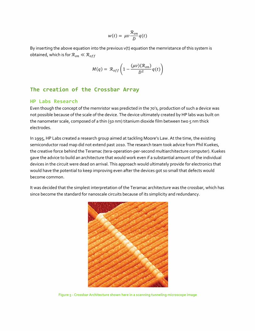
Figure 5 - Crossbar Architecture shown here in a scanning tunneling microscope image

Figure 6CROSSBAR ARCHITECTURE: A memristor’sstructure, shown here in a scanning tunneling microscope image
Crossbar Array
The Crossbar Array is an array of perpendicular wires. Anywhere two perpendicular wires cross, there is
a switch connecting them. In order to connect any horizontal wire to a vertical wire at any orientation
on the grid, the switch sandwiched between those two wires must be closed. The general idea was to
enable communication by opening and closing these switches by applying voltages to the ends of the
wires. By this description, it is fair a describe a crossbar array as basically a storage system, with an
open switch representing a zero and a closed switch representing a one.
Crossbar Arrays use a wealth of redundancy, ensuring that any defect present in the device can be
avoided. Also, because of their simplicity, crossbar arrays have a much higher density of switches than a
comparable integrated circuit based on transistors.
Figure 7 - Artist Rendering of Crossbar Array Configuration
A switch used in a crossbar array is a 40-nanometer cube of titanium dioxide (TiO2) which is expressed
in two separate layers: The lower layer of TiO2 has a perfect 2:1 oxygen-to-titanium ratio, making it an
exceptional insulator. In contrast, the upper layer of TiO2 is missing 0.5 percent of its oxygen (TiO2-x),
causing vacancies make the TiO2-x a conductive metallic material.

The engineered oxygen deficiencies in the TiO2-x manifest as oxygen vacancies scattered throughout
the upper layer. A positive voltage applied to the switch repels the positive oxygen deficiencies in the
metallic upper TiO2-x layer, sending them into the insulating TiO2 layer below. That causes the boundary
between the two materials to move down, increasing the conductivity of the entire switch. The more
positive voltage is applied, the more conductive the switch becomes.
A negative voltage on the switch attracts the positively charged oxygen particles, pulling them out of
the TiO2. This reaction renders the switch as a whole to become more resistive. The more negative
voltage is applied, the less conductive the cube becomes.
What makes this switch memristive is that when the voltage is turned off, positive or negative, the
oxygen bubbles do not migrate. They stay where they are, which means that the boundary between the
two titanium dioxide layers is frozen. That is how the memristor ‘remembers’ how much voltage was
last applied.
Connection to Chua’s Memristor
Leon Chua’s original predicted model for the hypothetical memristor’s behavior is shown in the figure
shown below. The graph produced my HP Labs’ research team’s experimental results is shown in the
following figure. The loops represent and map the switching behavior of the device. Both models begin
with a high resistance, and as the voltage increases, the current slowly increases. As charge flows
through the device, the resistance drops, and the current increases more rapidly with increasing voltage
until the maximum is reached. The results obtained by HP labs researcher’s is clearly suggestive of the
ideal memristor proposed by Chua.

Figure 9 - Leon Chua’s Predicted Model
Applications
Moore’s Law states that the density of transistors on an integrated circuit doubles about every 18
months. This rule of thumb has held true for more than 40 years, but there is an agreement in the
industry that the process of miniaturizing transistors will only be able to continue for about another
decade. The emphasis in design will have to change to devices that are not just increasingly
infinitesimal but are in fact increasingly capable.
When memristors are combined with transistors in a hybrid chip, memristors would be expected to
improve the performance of digital circuits without shrinking transistors from their current day
dimensions. The purpose is to use transistors more efficiently, and this process could potentially extend
the drop-off of Moore’s Law by another decade.
Instant-On Computers
The key feature of a memristor is that when the voltage is turned off, the device remembers the
resistance it was last at until. That resistance-saving property makes memristors very appealing for use
in computer memory.
The ability to always remember resistance values means that a memristor could be used as a
nonvolatile memory. If a laptop contained memory built using memristors, removing the battery from
the computer would not lose any memory. When the battery was returned, the computer would turn on
exactly where the user left off. Memristors would potentially be able to remove lengthy reboot or
unintentional loss of memory due to a power failure.
Figure 8 - HP labs Results for Crossbar Array Implementation

Brain circuits
One extremely interesting example of a potential application for memristors would be the creation of a
circuit that was able to mimic the processes of the human brain. Within a decade, memristors could
potentially allow mankind to properly emulate, instead of simply simulate, networks of neurons and
synapses.
Using current day transistors, the system needed to simulate a mouse brain in real time would involve
solving an astronomical number of partial differential equations. It is estimated that a digital computer
capable of this workload would need to be the size of a small city, and it would need to be powered by
several dedicated nuclear power plants.
In contrast, by using memristors instead of transistors, an electronic circuit that is theorized to be small
enough to fit in a shoebox, would be able to function according to the same physical principles as a
brain. This feat would be possible because memristors behave functionally like synapses, replacing a
few transistors in a circuit with memristors could lead to analog circuits that can think like a human
brain. A hybrid circuit which contains memristors and transistors could help scientists research actual
brain function and disorders.
The Future of the Memristor
For memristor based memory devices to become a reality, the reliable design and manufacture of
electrode contacts, interconnects and the active region of the memristor must be possible. Also,
because signal gain is not possible with a memristor, research needs to be put into creating a high
resistance ratio between the ON and OFF states. Fundamentally, a far deeper understanding of the
memristor is extremely important.
Transistors clearly have a steady hold on the current design market, and the idea of proposing an
alternative to a currently productive technology will be a steep slope to climb. Most manufacturers will
embrace this technology only after a well-functioning, large-scale array is clearly demonstrated. When
that demonstration occurs, there will surely be a rejuvenated race towards smaller devices.

Work Cited
D B Strukovet al, Nature, 2008, 453, 80
"Dr. Leon O. Chua." Scholarpedia. 8 Mar. 2009 <http://www.scholarpedia.org/article/User:Chua>.
Leon O. Chua. University of California, Berkeley. 8 Mar. 2009 <http://www.eecs.berkeley.edu/~chua/>.
"Leon O. Chua." Wikipedia Foundation, Inc. 8 Mar. 2009 <http://en.wikipedia.org/wiki/Leon_O._Chua>.
"Nanotechnology." 2009. Hewlett-Packard Development Company, L.P. 8 Mar. 2009
<http://www.hpl.hp.com/research/about/nanotechnology.html>.
R. Stanley Williams, How We Found the Missing Memristor, IEEE Spectrum, December 2008
"Towards Molecular Electronics: New Way of Making Molecular Transistors." PhysOrg.com. 8 Mar.
2009 <http://www.physorg.com/news10092.html>.


