TI DesignsRS-232 Full Modem Interface (8-Wire) Module forProtection Relay, IED, and Substation AutomationReference Design
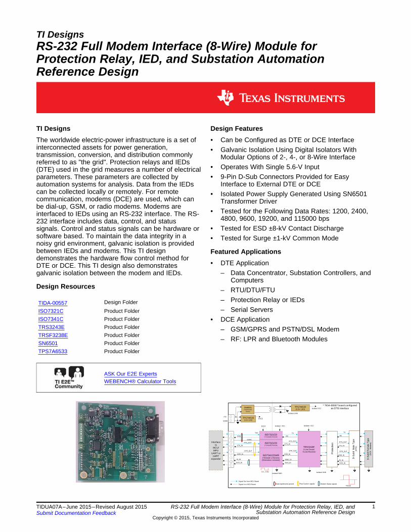
TI Designs Design FeaturesThe worldwide electric-power infrastructure is a set of • Can be Configured as DTE or DCE Interfaceinterconnected assets for power generation, • Galvanic Isolation Using Digital Isolators Withtransmission, conversion, and distribution commonly Modular Options of 2-, 4-, or 8-Wire Interfacereferred to as "the grid". Protection relays and IEDs
• Operates With Single 5.6-V Input(DTE) used in the grid measures a number of electrical• 9-Pin D-Sub Connectors Provided for Easyparameters. These parameters are collected by
Interface to External DTE or DCEautomation systems for analysis. Data from the IEDscan be collected locally or remotely. For remote • Isolated Power Supply Generated Using SN6501communication, modems (DCE) are used, which can Transformer Driverbe dial-up, GSM, or radio modems. Modems are
• Tested for the Following Data Rates: 1200, 2400,interfaced to IEDs using an RS-232 interface. The RS-4800, 9600, 19200, and 115000 bps232 interface includes data, control, and status
• Tested for ESD ±8-kV Contact Dischargesignals. Control and status signals can be hardware orsoftware based. To maintain the data integrity in a • Tested for Surge ±1-kV Common Modenoisy grid environment, galvanic isolation is providedbetween IEDs and modems. This TI design Featured Applicationsdemonstrates the hardware flow control method for
• DTE ApplicationDTE or DCE. This TI design also demonstrates– Data Concentrator, Substation Controllers, andgalvanic isolation between the modem and IEDs.
ComputersDesign Resources – RTU/DTU/FTU
– Protection Relay or IEDsDesign FolderTIDA-00557– Serial ServersISO7321C Product Folder
ISO7341C Product Folder • DCE ApplicationTRS3243E Product Folder – GSM/GPRS and PSTN/DSL ModemTRSF3238E Product Folder – RF: LPR and Bluetooth ModulesSN6501 Product FolderTPS7A6533 Product Folder
ASK Our E2E ExpertsWEBENCH® Calculator Tools
1TIDUA07A–June 2015–Revised August 2015 RS-232 Full Modem Interface (8-Wire) Module for Protection Relay, IED, andSubstation Automation Reference DesignSubmit Documentation Feedback
Signal From the MCU Board Data signals plus ground
SGND
Flow Control signals
3.3 ± 5.5V
Modem Status signals
Interface to
MCU/MPU
UART or UART
expander
+5V
SGND
Isolated GND
SN6501(Transformer
Driver)
TPS7A6533(3.3V LDO) Isolated VCC
DVCCTPS7A6533(3.3V LDO)
Isolated VCC
TXD ( RXD of MCU)
RXD( TXD of MCU )
* TIDA-00557 board configured as DCE Interface
TRSF3238E
Key System Specifications www.ti.com
An IMPORTANT NOTICE at the end of this TI reference design addresses authorized use, intellectual property matters and otherimportant disclaimers and information.
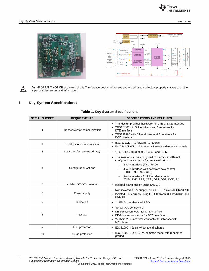
1 Key System Specifications
Table 1. Key System Specifications
SERIAL NUMBER REQUIREMENTS SPECIFICATIONS AND FEATURES
• This design provides hardware for DTE or DCE interface• TRS3243E with 3 line drivers and 5 receivers for
1 Transceiver for communication DTE interface• TRSF3238E with 5 line drivers and 3 receivers for
2 System DescriptionThis design provides an interface for a true RS-232 (eight signal+ground) physical layer interface for dataterminal equipment (DTE) using a DB-9 plug-type connector with a provision for a data communicationequipment (DCE) interface.
TI’s RS-232 interface devices are commonly used in IEDs and protection relays. These devices generatetheir own higher voltage to drive the RS-232 and operate with 3.3 to 5.0 V.
TI’s RS-232 devices also offer ESD protection up to ±15-kV air discharge as per IEC61000-4-2, higherdata transfer rates, and auto-powerdown functionality that reduces power consumption significantly.
This design also shows galvanic isolation implementation between the MCU and RS-232 transceiver usingTI digital isolators. This TI design also showcase small form factor isolated DC-DC converters usingmonolithic oscillator and power driver.
This TI design also shows a modular way of implementing the 2-wire RS-232 using TXD, RXD, andground, 4-wire interface using TXD, RXD, RTS, CTS, and ground, and 8-wire RS-232 using TXD, RXD,RTS, CTS, DTR, DSR, DCD, RI, and ground using the DB-9 connector.
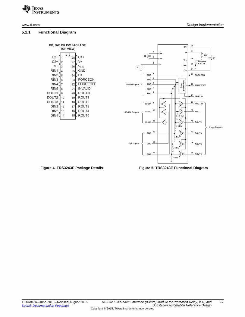
2.1 RS-232 TransceiverThis uses the TRS3243E RS-232 transceiver for DTE interfaces. The TRS3243E device consists of threeline drivers, five line receivers, and a dual charge-pump circuit with ±15-kV ESD (HBM and IEC61000-4-2,air-gap discharge) and ±8-kV ESD (IEC61000-4-2, contact discharge) protection on serial-port connectionpins. The device meets the requirements of TIA/EIA-232-F and provides the electrical interface betweenan asynchronous communication controller and the serial-port connector.
If this design has to be used for a DCE interface requirement, then the TRSF3238E interface section hasto be populated alone along with power supply.
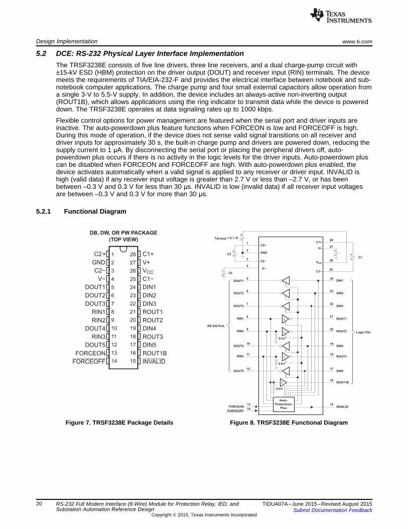
The TRSF3238E consists of five line drivers, three line receivers, and a dual charge-pump circuit with±15-kV ESD (HBM) protection on the driver output (DOUT) and receiver input (RIN) terminals. The devicemeets the requirements of TIA/EIA-232-F.
2.2 Digital IsolatorsThe ISO7321C provides galvanic isolation up to 3000 VRMS for one minute per UL and 4242 VPK per VDE.These devices have two isolated channels comprised of logic input and output buffers separated by silicondioxide (SiO2) insulation barriers. The ISO7321C has the two channels in opposite direction.
The ISO7341C provides galvanic isolation up to 3000 VRMS for one minute per UL and 4242 VPK per VDE.These devices have four isolated channels comprised of logic input and output buffers separated by aSiO2 insulation barrier. The ISO7341C has three forward and one reverse-direction channels.
2.3 Transformer Driver for Isolated Power SupplyThe SN6501 Transformer Driver is used for generating isolated power. The SN6501 is a monolithicoscillator and power driver, specifically designed for small form factor, isolated power supplies in isolatedinterface applications.
2.4 LDOThe LDO TPS7A6533-Q1 is used in this design to generate 3.3 V for an isolated or non-isolatedpower supply.
3TIDUA07A–June 2015–Revised August 2015 RS-232 Full Modem Interface (8-Wire) Module for Protection Relay, IED, andSubstation Automation Reference DesignSubmit Documentation Feedback
Signal From the MCU Board Data signals plus ground
SGND
Flow Control signals
3.3 ± 5.5V
Modem Status signals
Interface to
MCU/MPU
UART or UART
expander
+5V
SGND
Isolated GND
SN6501(Transformer
Driver)
TPS7A6533(3.3V LDO) Isolated VCC
DVCCTPS7A6533(3.3V LDO)
Isolated VCC
TXD ( RXD of MCU)
RXD( TXD of MCU )
* TIDA-00557 board configured as DCE Interface
TRSF3238E
Block Diagram www.ti.com
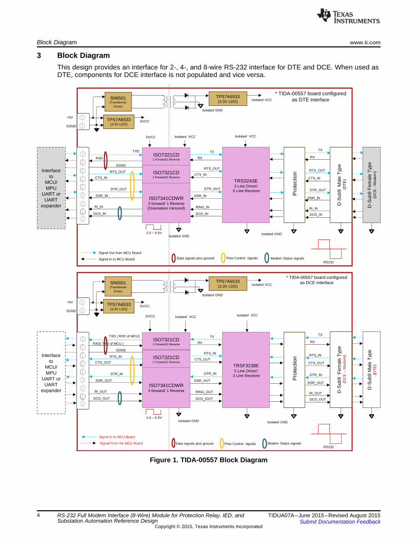
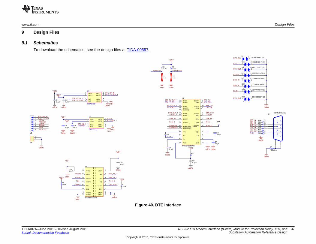
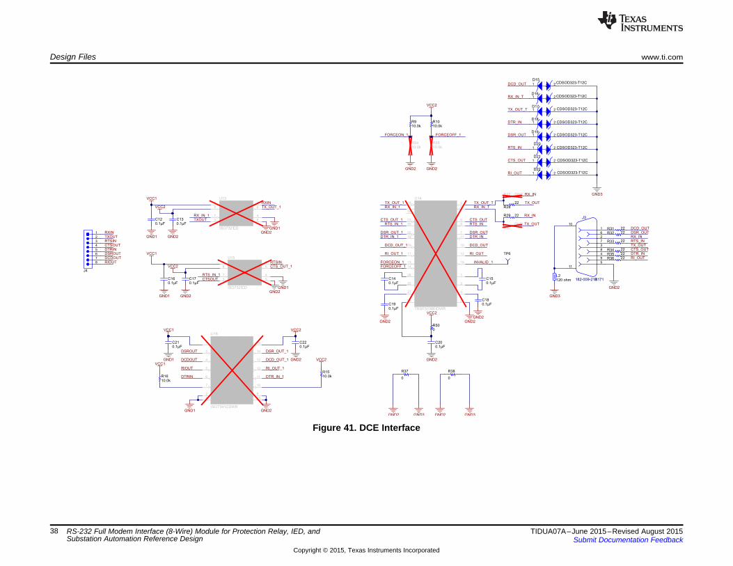
3 Block DiagramThis design provides an interface for 2-, 4-, and 8-wire RS-232 interface for DTE and DCE. When used asDTE, components for DCE interface is not populated and vice versa.
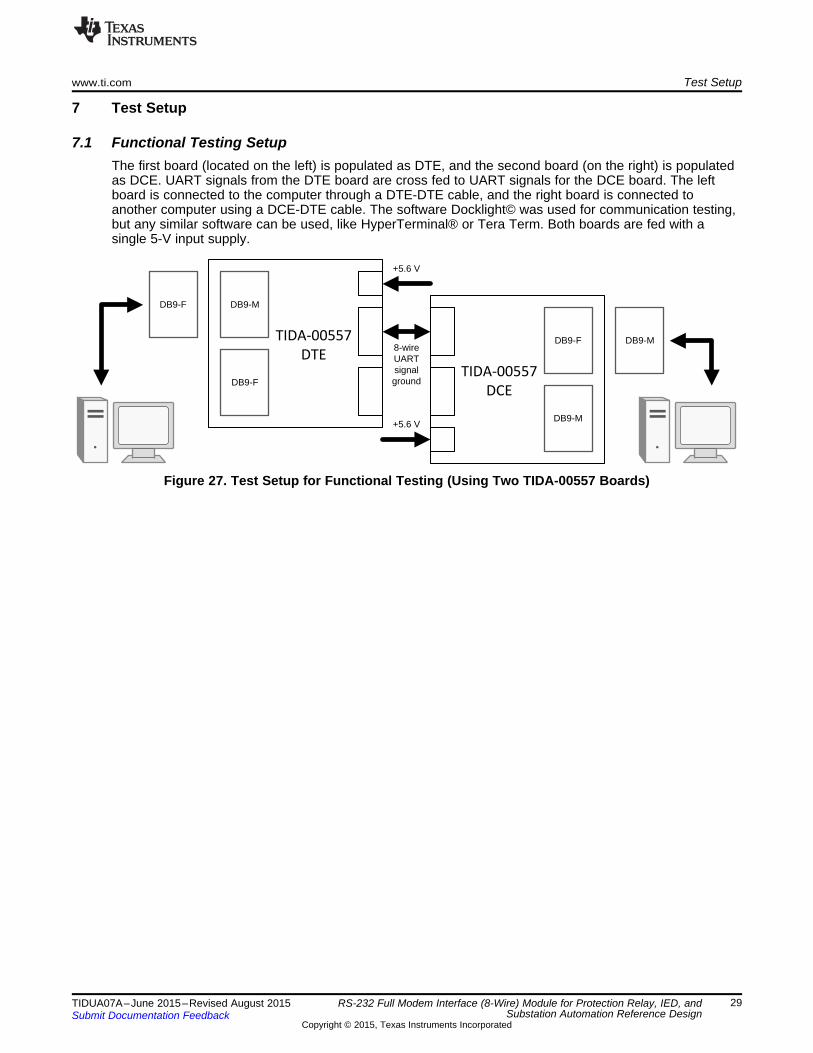
Figure 1. TIDA-00557 Block Diagram
4 RS-232 Full Modem Interface (8-Wire) Module for Protection Relay, IED, and TIDUA07A–June 2015–Revised August 2015Substation Automation Reference Design Submit Documentation Feedback
3.1.1 TRS3243EThe TRS3243E device consists of three line drivers, five line receivers, and a dual charge-pump circuitwith ±15-kV ESD (HBM and IEC61000-4-2, air-gap discharge) and ±8-kV ESD (IEC61000-4-2, contactdischarge) protection on serial-port connection pins. The device meets the requirements of TIA/EIA-232-Fand provides the electrical interface between an asynchronous communication controller and the serial-port connector. It has following features:• Single-chip and single-supply interface for IBM™ PC/AT™ serial port• ESD protection for RS-232 bus pins:
– ±8-kV IEC61000-4-2, contact discharge– ±15-kV IEC61000-4-2, air-gap discharge– Meets or exceeds requirements of TIA/EIA-232-F and ITU v.28 standards– Operates with 3-V to 5.5-V VCC supply– Always-active non-inverting receiver output (ROUT2B)– Data rate of 500 kb/s for TRS3243E– Low standby current: 1 μA typical– External capacitors: 4 × 0.1 μF– Accepts 5-V logic input with 3.3-V supply– Designed to be interchangeable with industry standard 3243E devices– Serial-mouse driveability– Auto-powerdown feature to disable driver outputs when no valid RS-232 signal is sensed– Package options include plastic small-outline (DW), shrink small-outline (DB), and thin shrink small-
outline (PW) packages
3.1.2 TRSF3238EThe TRSF3238E consists of five line drivers, three line receivers, and a dual charge-pump circuit with±15-kV ESD (HBM) protection on the driver output (DOUT) and receiver input (RIN) terminals. The devicemeets the requirements of TIA/EIA-232-F and provides the electrical interface between notebook and sub-notebook computer applications. The charge pump and four small external capacitors allow operation froma single 3-V to 5.5-V supply. In addition, the device includes an always-active non-inverting output(ROUT1B), which allows applications using the ring indicator to transmit data while the device is powereddown. It has following features:• RS-232 bus-pin ESD protection exceeds ±15 kV using HBM• Meets or exceeds the requirements of TIA/EIA-232-F and ITU v.28 standards• Operates with 3-V to 5.5-V VCC supply• Data rate of up to 1 Mbps• Five drivers and three receivers• Auto-power down plus feature enables flexible power-down mode• Low standby current: 1 μA typical• External capacitors: 4 × 0.1 μF• Accept 5-V logic input with 3.3-V supply• Always-active non-inverting receiver output (ROUT1B)• ESD protection for RS-232 interface pins:
3.1.3 ISO7321CThe ISO7321C provides galvanic isolation up to 3000 VRMS for one minute per UL and 4242 VPK per VDE.These devices have two isolated channels comprised of logic input and output buffers separated by SiO2insulation barriers. The ISO7321C has the two channels in opposite direction. It has following features:• Signaling rate: 25 Mbps• Integrated noise filter on the inputs• Default output "high" and "low" options• Low power consumption — Typical ICC per channel at 1 Mbps:
– ISO7320: 1.2 mA (5-V supplies), 0.9 mA (3.3-V supplies)– ISO7321C: 1.7 mA (5-V supplies), 1.2 mA (3.3-V supplies)
– System-level ESD, EFT, and Surge immunity– Low emissions
• Isolation barrier life: > 25 years• Operates from 3.3-V and 5-V supplies• Narrow body SOIC-8 package• Safety and regulatory approvals:
– 4242 VPK isolation per DIN V VDE V 0884-10 and DIN EN 61010-1– 3000-VRMS isolation for one minute per UL 1577– CSA component acceptance notice 5 A, IEC 60950-1 and IEC 61010-1 standards– CQC certification per GB4943.1-2011
6 RS-232 Full Modem Interface (8-Wire) Module for Protection Relay, IED, and TIDUA07A–June 2015–Revised August 2015Substation Automation Reference Design Submit Documentation Feedback
3.1.4 ISO7341CThe ISO7341C provides galvanic isolation up to 3000 VRMS for one minute per UL and 4242 VPK per VDE.These devices have four isolated channels comprised of logic input and output buffers separated by aSiO2 insulation barrier. The ISO7341C has three forward and one reverse-direction channels.
The ISO7341C has an integrated noise filter for harsh industrial environment where short noise pulsesmay be present at the device input pins. The ISO7341C has TTL input thresholds and operates from3- to 5.5-V supply levels. Through innovative chip design and layout techniques, the EMC of theISO7341C has been significantly enhanced to enable system-level ESD, EFT, Surge, and emissionscompliance. It has following features:• Signaling rate: 25 Mbps• Integrated noise filter on the inputs• Default output "high" and "low" options• Low power consumption, typical ICC per channel at 1 Mbps:
– ISO7341C: 1.2 mA (5-V supplies), 0.9 mA (3.3-V supplies)• Low propagation delay: 31 ns typical (5-V supplies)• 3.3-V and 5-V level translation• Wide temperature range: –40°C to 125°C• 70-kV/μs transient immunity, typical (5-V supplies)• Robust EMC
– System-level ESD, EFT, and Surge immunity– Low emissions
• Operates from 3.3-V and 5-V supplies• Wide body SOIC-16 package
7TIDUA07A–June 2015–Revised August 2015 RS-232 Full Modem Interface (8-Wire) Module for Protection Relay, IED, andSubstation Automation Reference DesignSubmit Documentation Feedback
3.1.5 SN6501The SN6501 is a monolithic oscillator and power driver, specifically designed for small form factor, isolatedpower supplies in isolated interface applications. It drives a low-profile, center-tapped transformer primaryfrom a 3.3-V or 5-V DC power supply. The secondary can be wound to provide any isolated voltage basedon transformer turns ratio. The SN6501 consists of an oscillator followed by a gate drive circuit thatprovides the complementary output signals to drive the ground-referenced, N-channel power switches.The internal logic ensures break-before-make action between the two switches. The SN6501 is availablein a small SOT23-5 package, and is specified for operation at temperatures from –40°C to 125°C. It hasfollowing features:• Push-pull driver for small transformers• Single 3.3-V or 5-V supply• High primary-side current drive:
– 5-V supply: 350 mA (maximum)– 3.3-V supply: 150 mA (maximum)
• Low ripple on rectified output permits small output capacitors• Small 5-pin SOT-23 package
3.1.6 TPS7A6533-Q1The TPS7A6533-Q1 is a low-dropout linear voltage regulator designed for low power consumption and aquiescent current less than 25 μA in light-load applications. This device features integrated overcurrentprotection and a design to achieve stable operation even with low-ESR ceramic output capacitors. It hasfollowing features:• Low dropout voltage:
– 300 mV at IOUT = 150 mA• 4-V to 40-V wide input voltage range with up to 45-V transients• 300-mA maximum output current• 25-μA (typical) ultra-low quiescent current at light loads• 3.3-V and 5-V fixed output voltage with ±2% tolerance• Low-ESR ceramic output stability capacitor• Integrated fault protection
– Short-circuit and overcurrent protection– Thermal shutdown
• Low-input voltage tracking• Thermally enhanced power package
– 3-pin TO-252 (KVU/DPAK)
8 RS-232 Full Modem Interface (8-Wire) Module for Protection Relay, IED, and TIDUA07A–June 2015–Revised August 2015Substation Automation Reference Design Submit Documentation Feedback
4 System Design TheoryThe following section describes the RS-232 physical layer interface in general and the implementation ofthe RS-232 interface with galvanic isolation using TI devices.
4.1 Introduction to RS-232 Communication and Digital IsolationThe worldwide electric-power infrastructure is a set of interconnected assets for power generation, transmission,conversion, and distribution commonly referred to as "the grid". Protection relays and IEDs (DTE) used in the gridmeasures a number of electrical parameters. These parameters are collected by automation systems foranalysis. Data from the IEDs can be collected locally or remotely. For remote communication, modems (DCE)are used, which can be dial-up, radio, or GSM modems. Modems interface to IEDs using an RS-232 interface.The RS-232 interface includes data, control, and status signals. To maintain the data integrity in noisy gridenvironments, galvanic isolation is preferred between IEDs and modems. This TI design demonstrates thehardware flow control method for DTE or DCE. This TI design also demonstrates galvanic isolation between theinternal signal processing system and the external world using digital isolators.
4.1.1 Serial Communication Using RS-232The RS-232 interface is used as a standard communication interface involving modem communicationbetween the two devices or equipment.
The RS-232 interface is the Electronic Industries Association (EIA) standard for the interchange of serialbinary data between two devices. It was initially developed by the EIA to standardize the connection ofcomputers with telephone line modems. This standard defines both the electrical and functionalcharacteristics of the various serial interface circuits.
TIA/EIA-232-F Industry Standard for Data TransmissionThe EIA introduced the 232 standard in 1962 in an effort to standardize the interface between DTE andDCE. The DTE comprises the data source, data link, or both. The DCE provides the functions to establish,maintain, and terminate a connection, and to code or decode the signals between the DTE and the datachannel. Although an emphasis then was placed on interfacing between a modem unit and DTE, otherapplications were quick to adopt the 232 standard. The growing use of the personal computer (PC) quicklyensured that 232 became the industry standard for all low-cost serial interfaces between the DTE andperipheral. The mouse, plotter, printer, scanner, digitizer, and tracker ball, in addition to the externalmodems and test equipment, are all examples of peripherals that connect to a 232 port. Using a commonstandard allows widespread compatibility, plus a reliable method for interconnecting a PC to peripheralfunctions.
The EIA RS-232-C standard, revised in 1969, was superseded by EIA-232-D (1986). The EIA-232-D againwas superseded by TIA/EIA-232-E, which brings it in line with ITU V.24, V.28, and ISO IS2110. Thisrevision includes an update on the rise-time to unit-interval ratio and reverses the changes made by the Drevision (see Figure 2). Although an older standard with problems such as high noise susceptibility, lowdata rates, and very limited transmission length, 232 fulfills a vital need as a low-cost communicationsystem. Consequently, new products are being developed at a faster rate than ever. The most recentrevision is the TIA/EIA-232-F, which does not have any technical changes that will create compatibilityproblems with equipment conforming to previous revisions of TIA/EIA-232. This latest version brings it inline once again with international standards ITU-T V.24, V.28, and ISO/IEC 2110.
9TIDUA07A–June 2015–Revised August 2015 RS-232 Full Modem Interface (8-Wire) Module for Protection Relay, IED, andSubstation Automation Reference DesignSubmit Documentation Feedback
Signal Interface Line (1 of 25 Maximum) Interchange Signal
Receiver Input Impedance, 3 kΩ to 7 kΩ
Driver Power-Off Impedance, >300 Ω
Load Capacitance <2500 pF Includes
Receiver Input
Tx Rise/Fall Time Within Transition Region
1 ms – Below 40 bit/s
4% of Unit Interval – 30 bit/s to 20 kbit/s
Slew Rate: 30 V/µs max
?
System Design Theory www.ti.com
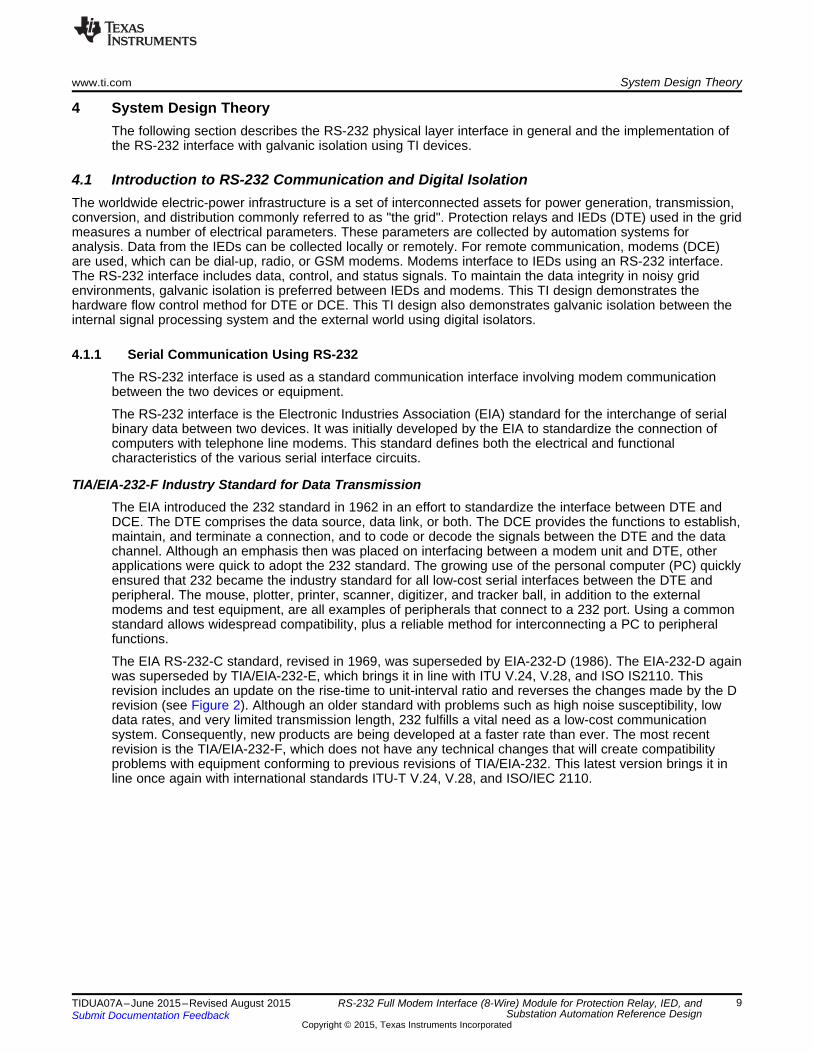
TIA/EIA-232-F Electrical SpecificationAll RS-232 circuits carry voltage signals with the voltage at the connector pins not to exceed ±25 V. Allpins must be able to withstand a short circuit to any other pin without sustaining permanent damage. Eachline should have a minimum load of 3 kΩ and a maximum load of 7 kΩ, which usually is part of thereceiver circuit. A logic of 0 is represented by a driven voltage between 5 V and 15 V and a logic of 1between –5 V and –15 V. At the receiving end, a voltage between 3 V and 15 V represents a 0 and avoltage of between –3 V and –15 V represents a 1. Voltages between ±3 V are undefined and lie in thetransition region. This effectively gives a 2-V minimum noise margin at the receiver. The maximum cablelength originally was defined in RS-232-C as 15 meters; however, this has been revised in EIA-232-D andTIA/EIA-232-E and is now specified more correctly as a maximum capacitive load of 2500 pF. Thisequates to about 15 to 20 meters of line length, depending on cable capacitance.
Figure 2. RS-232-F Electrical Specification
The RS-232 specifies a maximum slew rate of the signal at the output of the driver to be 30 V/μs. Thislimitation is concerned with the problem of crosstalk between conductors in a multi-conductor cable. Thefaster the transition edge, the greater the amount of crosstalk. This restriction, together with the fact thatthe drivers and receivers use a common signal ground and the associated noise introduced by the groundcurrent, severely limits the maximum data throughput.
One can extrapolate this further by using the 4% figure. With the maximum slew rate of 30 V/μs, themaximum achievable data rate is 200 kbps; however, in practice, this is limited to around 120 kbps. Anumber of software programs operate at transfer rates of 116 kbps. Furthermore, over longer line lengths,the maximum drive current of the line driver becomes the dominant feature affecting data rate, displacingthe 30-V/μs slew rate. As the line length increases, the load capacitance also increases, requiring morecurrent to maintain the same transition time.
10 RS-232 Full Modem Interface (8-Wire) Module for Protection Relay, IED, and TIDUA07A–June 2015–Revised August 2015Substation Automation Reference Design Submit Documentation Feedback
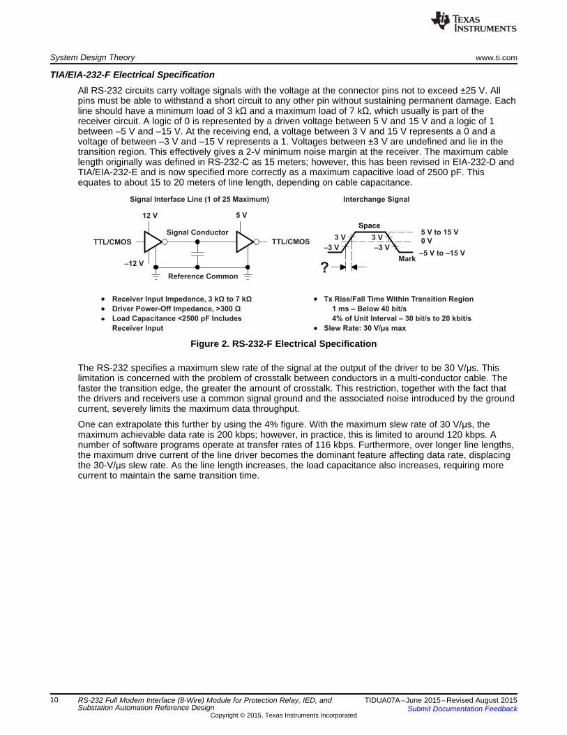
1. Data Carrier Detect (CD)2. Receive Data (RD)3. Transmit Data (TD)4. Data Terminal Ready (DTR)5. Ground6. Data Set Ready (DSR)7. Request To Send (RTS)8. Clear To Send (CTS)9. Ring Indicator (RI)
DB-9 Connector:
www.ti.com System Design Theory
TIA/EIA-232-F Mechanical SpecificationThe RS-232 standard supports two types of connectors: a 25-pin D-type connector (DB-25) and a 9-pinD-type connector (DB-9). Figure 3 shows the pin diagram of the DB-9 connector, which is also used in thecurrent TI design.
Figure 3. DB-9 Connector Pin Details
Although RS-232 specifies a 25-pin connector, this connector is often not used. Most applications do notrequire all the defined signals, so a 25-pin connector is larger than necessary. The most popularconnector is the 9-pin DB9 connector, which provides the necessary signals for the serial communicationin modem applications. Table 2 contains the functional details of all eight signals used with the DB-9connector. RS-232 signals have a direction (in or out) depending on whether they are with respect to aDTE or a DCE.
Table 2. RS-232 Signal Details
DB-9 PIN NO SIGNAL TYPE DIRECTION FUNCTIONDetermines whether the DCE is connected to a working1 CD Control DCE to DTE phone line or not (only used in connection with modem).
2 TD Data DTE to DCE Computer (DTE) sends information to the DCE.Computer (DTE) receives information sent from the3 RD Data DCE to DTE DCE.Computer (DTE) tells the DCE that it is ready tocommunicate. Raised by DTE when powered on. In4 DTR Control DTE to DCE auto-answer mode raised only when RI arrives fromDCE.
5 SG Ground — Signal groundModem (DCE) tells the computer that it is ready to talk.6 DSR Control DCE to DTE Raised by DCE to indicate ready.Computer (DTE) asks the modem if it can send
7 RTS Control DTE to DCE information. Raised by DTE when it wishes to send.Expects CTS from DCE.Modem (DCE) tells the computer (DTE) that it can send
8 CTS Control DCE to DTE information. Raised by DCE in response to RTS fromDTE.Set when incoming ring detected, used for auto-answer
9 RI Control DCE to DTE application. DTE raises DTR to answer (only used inconnection with modem).
11TIDUA07A–June 2015–Revised August 2015 RS-232 Full Modem Interface (8-Wire) Module for Protection Relay, IED, andSubstation Automation Reference DesignSubmit Documentation Feedback
TIA/EIA-232-F Handshaking OptionsConnections and Signal Flow ControlFlow control is the process of managing the rate of data transmission between two nodes to prevent a fastsender from over running a slow receiver. For example, as DTE-to-DCE speed is a few times faster thanDCE-to-DTE speed, the PC can send data to the modem at a higher rate. That means in this connectionsooner or later the data may be lost because of the buffers overflow, so the control of data flow should berealized.
Flow control mechanisms can be classified by whether or not the receiving node sends feedback to thesending node. That is through a "handshake", an exchange of characters between a transmitter and areceiver is used to postpone transmission until the receiver is ready to receive the data. This characterflow control is of two main types: Software and hardware.
Software Flow ControlOne example is "Xon/Xoff". The two characters Xon and Xoff are used control the data flow. Xon isusually 17 characters, and Xoff is 19 characters. The modem will only have a small buffer. When thecomputer fills it, the modem sends an Xoff character to inform the computer about data transfertermination. As soon as the modem empties most of the memory for data, it will send the Xon character tothe computer and start the data transfer again. The main advantage of this type of data flow control is thatit does not need any other wires as the characters are sent through TD/RD lines. But if the connection isslow, every character needs 10 bits, which can reduce the connection speed.
Hardware Flow ControlMost serial communications uses software flow control, but there is an alternative: hardware handshaking.Hardware flow control is also known as RTS/CTS flow control. To realize this control, two additional wires(RTS and CTS) in the sequential cable are used. This results in increasing the data transmission rate, asno time is spent for Xon-Xoff characters transmission
Null Modem ConnectionsThe serial communication standards show the use of DTE/DCE communication, the way a computershould communicate with a peripheral device like a modem. But in a null modem connection, the PCs areconnected back-to-back with cables, each acting as a DTE, which means there is no DCE in this case.This type of connection finds many uses. The null modem can be configured in many ways using thenumber of signal lines available. In most situations, the original modem signal lines are reused to performsome sort of handshaking.
Handshaking has many advantages. It can increase the maximum allowed communication speed becausethen the computer will be able to control the flow of information. In a null modem connection without "flowcontrol", the communication may be possible only at the speed at which the receiving side can handle theamount of data.
Used in null modem connections, there are different types of flow control signals used in RS-232. The firsttwo flow control pins are known as request to send (RTS), an output signal from the DTE that comes asthe input for the DCE, and clear to send (CTS), which comes as the answering signal from the DCE side.Before sending a character, the DTE asks permission by setting its RTS output. No information will besent until the DCE grants permission by making the CTS line high.
The other two flow control signals, data terminal ready (DTR) and data set ready (DSR), are used tosignal the status of one communication side to the other. The DTE uses the DTR signal to signal that it isready to accept information, whereas the DCE uses the DSR signal for the same purpose. The last flowcontrol signal present in DTE/DCE communication is the CD carrier detect. It is not used directly for flowcontrol, but indicates the existence of a communication link between two modem devices.
12 RS-232 Full Modem Interface (8-Wire) Module for Protection Relay, IED, and TIDUA07A–June 2015–Revised August 2015Substation Automation Reference Design Submit Documentation Feedback
4.1.2 Isolated CommunicationComputer and industrial serial interfacing are areas where noise can seriously affect the integrity of datatransfer. A tested method of improving noise performance for any interface circuit is galvanic isolation.Isolation in data communication systems is achieved without a direct galvanic connection (wires) betweendrivers and receivers. Magnetic linkage from transformers provides the power for the system, and TI'scapacitively-coupled digital isolators provide the data connection. Galvanic isolation removes ground-loopcurrents, and the resulting noise voltage that corrupts data is eliminated. Also, common-mode noiseeffects and many forms of radiated noise can be reduced to negligible limits using this technique.
Unwanted currents and voltages on a cable bus connecting multiple systems could potentially causesevere problems. High voltages and currents can destroy components connected to the bus. Theseunwanted voltages and currents come primarily from two sources: ground loops and electrical line surges.
Ground loops occur when a bus or system uses multiple ground paths. It cannot be assumed that twosystem grounds connected to the bus and separated by hundreds or thousands of meters will be at thesame potential. These grounds are unlikely to be at the same potential; current will flow between thesepoints. This unintended current flow can damage or destroy components.
Electrical surges can be caused by many sources, the result of currents coupled onto cable lines throughinduction. Long cable lines in industrial environments are especially susceptible to this phenomena. Theoperation of electric motors, in particular, causes rapid changes in the ground potential. These changescan generate a current flow through any nearby lines to equalize the ground potential.
Other induction surge sources include electrostatic discharge (ESD) and lightning strikes. These inducedsurges can result in hundreds, or even thousands of volts of potential on the line, and manifest themselvesas transient current and voltage surges. Therefore, a remote node may receive a 5-V switching signalsuperimposed on a high voltage level with respect to the local ground. These uncontrolled voltages andcurrents can corrupt the signal and be catastrophic to the device and system, causing damage ordestruction of the components connected to the bus and resulting in system failure.
RS-232 systems that run over long distances and connect multiple systems are especially susceptible tothese events. To protect against this potentially destructive energy, all devices on the bus and systemsconnected to the bus must be referenced to only one ground. Isolating the RS-232 system devices fromeach of the systems connected to the bus prevents ground loops and electrical surges from destroyingcircuits. Isolation prevents ground loops, as each system connected to RS-232 cable bus, and eachRS-232 circuit, has a separate and isolated ground. By referencing each RS-232 circuit only to oneground, ground loops are eliminated.
Isolation also allows the RS-232 circuit reference voltage levels to rise and fall with any surges that appearon the cable line. Allowing the circuit voltage reference to move with surges, rather than being clamped toa fixed ground, prevents devices from being damaged or destroyed. To accomplish system isolation, boththe RS-232 signal lines and power supplies must be isolated. Power isolation is obtained through the useof an isolated DC-to-DC power supply. Signal isolation is typically accomplished with opto-couplers or withTI digital isolators.
Isolated Communication ImplementationRS-232 system signal path isolation is accomplished by designing isolators into the digital signal pathbetween the RS-232 driver and receiver and the local system. The isolator contains input and outputcircuits electrically isolated from one another. To complete the isolation of the RS-232 circuits from thelocal system, a DC-to-DC isolated power converter is required. The isolated power supply supplies powerto the local RS-232 driver, receiver, and RS-232 side of the isolator. The isolated power supply is typicallysupplied from the local system. The combination of digital isolators and an isolated DC-to-DC powersupply creates an effective protection against surge damage and eliminates ground loops
Isolation Device SelectionSystem performance requirements have the most impact on the selection of an isolation device. Otherconsiderations include space constraints and cost.
13TIDUA07A–June 2015–Revised August 2015 RS-232 Full Modem Interface (8-Wire) Module for Protection Relay, IED, andSubstation Automation Reference DesignSubmit Documentation Feedback
Data Rate RequirementsSystem data rate requirements are often the single most important parameter for device selection. If theRS-232 network runs at a lower data rate speed, there are more possible device selection options.
Device costs typically rise in proportion to data rate performance. Therefore, a designer should take carenot to specify a device with more performance than is required. However, a low-performance deviceselection can make future system performance upgrades more costly and involved, as all devicesincompatible with upgraded system data speeds will require replacement.
Space RequirementsSpace constraints are a second area of concern that can limit a designer’s choices. Maximum dimensionrequirements are a concern for virtually all applications. Some implementations can be severely spacelimited.
Cost RequirementsCost constraints and concerns are a reality in virtually all system design work. Cost considerations canhave an effect on the design choices for a system. As noted above, isolator device cost rises in proportionwith data rate performance. Specifying a device with only the system performance required can reducecosts. Other cost issues include a consideration of the number of devices used. Additional cost benefits ofintegrating as many channels into one device include reducing board space and assembly costs. A lowerdevice count results in smaller boards. Also, a lower device count typically results in a less complex boardlayout. The combination of smaller boards and less complex layout reduces board costs. In addition,circuit board assembly costs typically decrease proportionally as the number of devices required for theboard assembly process decreases, thus designing with fewer devices results in lower manufacturingcosts.
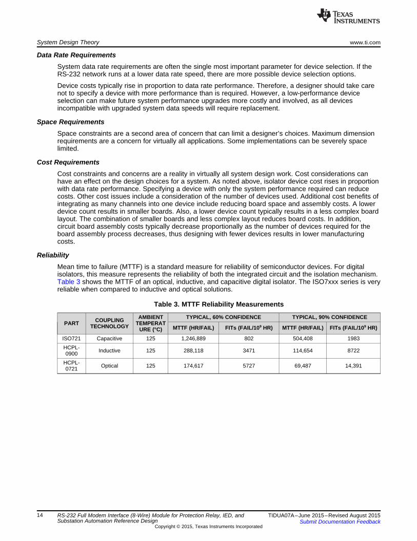
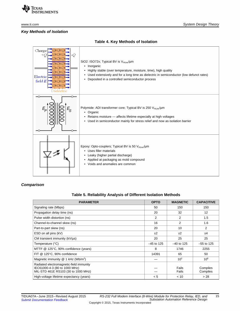
ReliabilityMean time to failure (MTTF) is a standard measure for reliability of semiconductor devices. For digitalisolators, this measure represents the reliability of both the integrated circuit and the isolation mechanism.Table 3 shows the MTTF of an optical, inductive, and capacitive digital isolator. The ISO7xxx series is veryreliable when compared to inductive and optical solutions.
SiO2: ISO72x; Typical BV is VPEAK/µm• Inorganic• Highly stable (over temperature, moisture, time), high quality• Used extensively and for a long time as dielectric in semiconductor (low defunct rates)• Deposited in a controlled semiconductor process
Polymide: ADI transformer core; Typical BV is 250 VPEAK/µm• Organic• Retains moisture — affects lifetime especially at high voltages• Used in semiconductor mainly for stress relief and now as isolation barrier
Epoxy: Opto-couplers; Typical BV is 50 VPEAK/µm• Uses filler materials• Leaky (higher partial discharge)• Applied at packaging as mold compound• Voids and anomalies are common
Comparison
Table 5. Reliability Analysis of Different Isolation Methods
5 Design ImplementationThis TI design has been configured as a DTE interface with an 8-wire true RS-232 interface. This boardcan be also configured as a DCE interface. Either a DTE or DCE interface can be used at a time withcomponents for the alternative interface un-populated on the PCB.
5.1 DTE: RS-232 Physical Layer Interface ImplementationThe TRS3243E device consists of three line drivers, five line receivers, and a dual charge-pump circuitwith ±15-kV ESD (HBM and IEC61000-4-2, air-gap discharge) and ±8-kV ESD (IEC61000-4-2, contactdischarge) protection on serial-port connection pins. The device meets the requirements of TIA/EIA-232-Fand provides the electrical interface between an asynchronous communication controller and the serial-port connector. This combination of drivers and receivers matches that needed for the typical serial portused in an IBM PC/AT or compatible. The charge pump and four small external capacitors allow operationfrom a single 3-V to 5.5-V supply. In addition, the device includes an always-active non-inverting output(ROUT2B), which allows applications using the ring indicator to transmit data while the device is powereddown. The device operates at data signaling rates up to 500 kb/s and a maximum of 30-V/μs driver outputslew rate.
Flexible control options for power management are available when the serial port is inactive. The auto-powerdown feature functions when FORCEON is low and FORCEOFF is high. During this mode ofoperation, if the device does not sense a valid RS-232 signal, the driver outputs are disabled. IfFORCEOFF is set low, both drivers and receivers (except ROUT2B) are shut off, and the supply current isreduced to 1 μA. Disconnecting the serial port or turning off the peripheral drivers causes the auto-powerdown condition to occur.
Auto-powerdown can be disabled when FORCEON and FORCEOFF are high and should be done whendriving a serial mouse. With auto-powerdown enabled, the device is activated automatically when a validsignal is applied to any receiver input. The INVALID output is used to notify the user if an RS-232 signal ispresent at any receiver input. INVALID is high (valid data) if any receiver input voltage is greater than2.7 V or less than –2.7 V or has been between –0.3 V and 0.3 V for less than 30 μs. INVALID is low(invalid data) if all receiver input voltages are between –0.3 V and 0.3 V for more than 30 μs.
16 RS-232 Full Modem Interface (8-Wire) Module for Protection Relay, IED, and TIDUA07A–June 2015–Revised August 2015Substation Automation Reference Design Submit Documentation Feedback
X X L X Z Powered offL H H X H Normal operation with auto-H H H X L powerdown disabledL L H Yes H Normal operation with auto-H L H Yes L powerdown enabled
Powered off by auto-powerdownX L H No Z feature(1) H = high level, L = low level, X = irrelevant, Z = high impedance
Table 8. Each Receiver (1)
INPUTS OUTPUTDRIVER STATUS
RIN FORCEON FORCEOFF ROUTX X L Z Powered offL X H H
Normal operation with auto-powerdownH X H L disabled and enabledOpen X H H
(1) H = high level, L = low level, X = irrelevant, Z = high impedance (off), Open = input disconnected or connected driver off
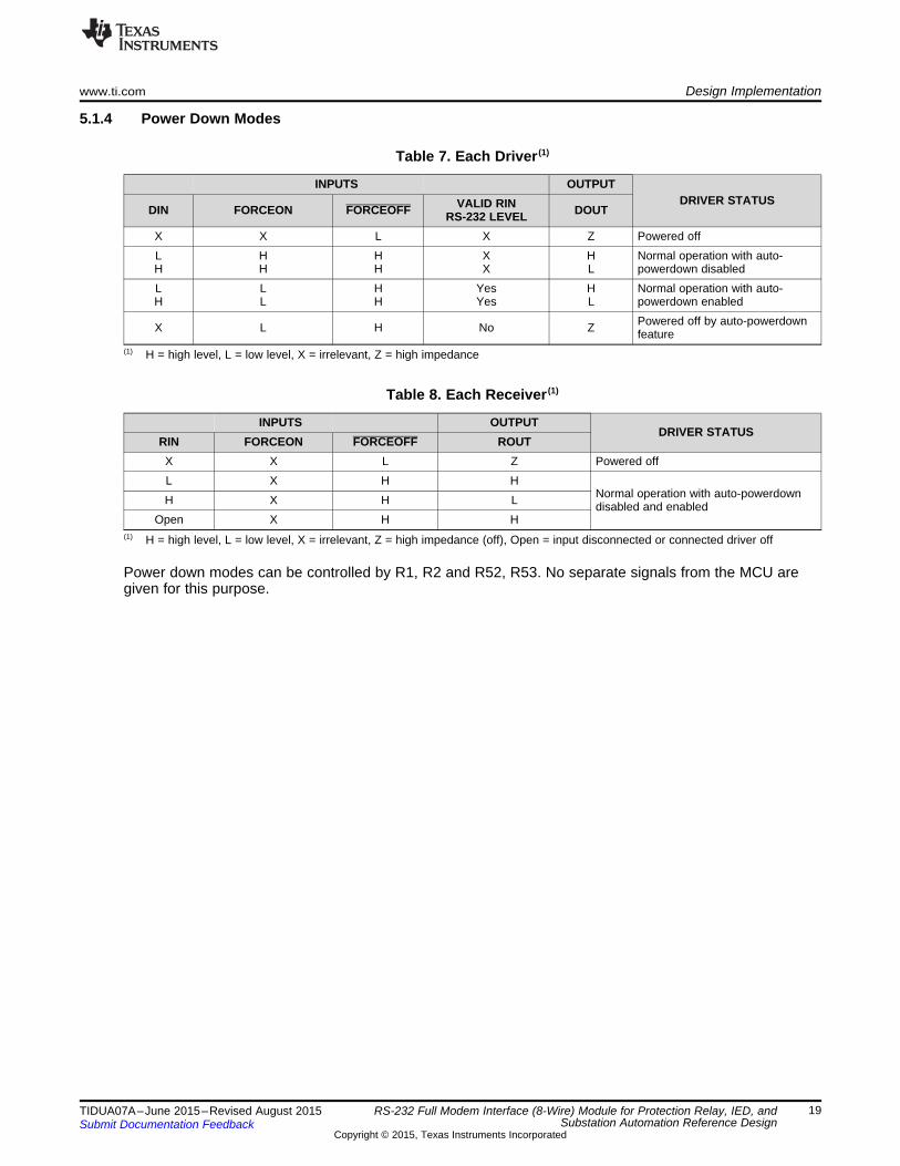
Power down modes can be controlled by R1, R2 and R52, R53. No separate signals from the MCU aregiven for this purpose.
19TIDUA07A–June 2015–Revised August 2015 RS-232 Full Modem Interface (8-Wire) Module for Protection Relay, IED, andSubstation Automation Reference DesignSubmit Documentation Feedback
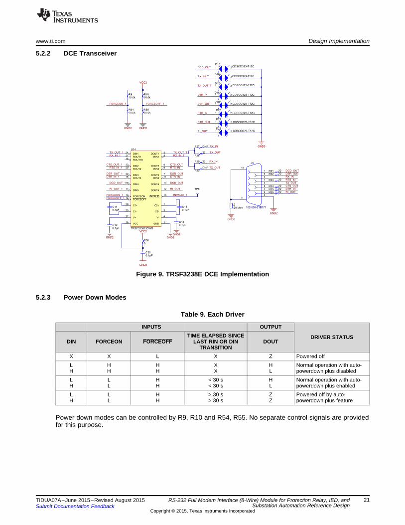
5.2 DCE: RS-232 Physical Layer Interface ImplementationThe TRSF3238E consists of five line drivers, three line receivers, and a dual charge-pump circuit with±15-kV ESD (HBM) protection on the driver output (DOUT) and receiver input (RIN) terminals. The devicemeets the requirements of TIA/EIA-232-F and provides the electrical interface between notebook and sub-notebook computer applications. The charge pump and four small external capacitors allow operation froma single 3-V to 5.5-V supply. In addition, the device includes an always-active non-inverting output(ROUT1B), which allows applications using the ring indicator to transmit data while the device is powereddown. The TRSF3238E operates at data signaling rates up to 1000 kbps.
Flexible control options for power management are featured when the serial port and driver inputs areinactive. The auto-powerdown plus feature functions when FORCEON is low and FORCEOFF is high.During this mode of operation, if the device does not sense valid signal transitions on all receiver anddriver inputs for approximately 30 s, the built-in charge pump and drivers are powered down, reducing thesupply current to 1 μA. By disconnecting the serial port or placing the peripheral drivers off, auto-powerdown plus occurs if there is no activity in the logic levels for the driver inputs. Auto-powerdown pluscan be disabled when FORCEON and FORCEOFF are high. With auto-powerdown plus enabled, thedevice activates automatically when a valid signal is applied to any receiver or driver input. INVALID ishigh (valid data) if any receiver input voltage is greater than 2.7 V or less than –2.7 V, or has beenbetween –0.3 V and 0.3 V for less than 30 μs. INVALID is low (invalid data) if all receiver input voltagesare between –0.3 V and 0.3 V for more than 30 μs.
DIN FORCEON FORCEOFF LAST RIN OR DIN DOUTTRANSITION
X X L X Z Powered offL H H X H Normal operation with auto-H H H X L powerdown plus disabledL L H < 30 s H Normal operation with auto-H L H < 30 s L powerdown plus enabledL L H > 30 s Z Powered off by auto-H L H > 30 s Z powerdown plus feature
Power down modes can be controlled by R9, R10 and R54, R55. No separate control signals are providedfor this purpose.
21TIDUA07A–June 2015–Revised August 2015 RS-232 Full Modem Interface (8-Wire) Module for Protection Relay, IED, andSubstation Automation Reference DesignSubmit Documentation Feedback
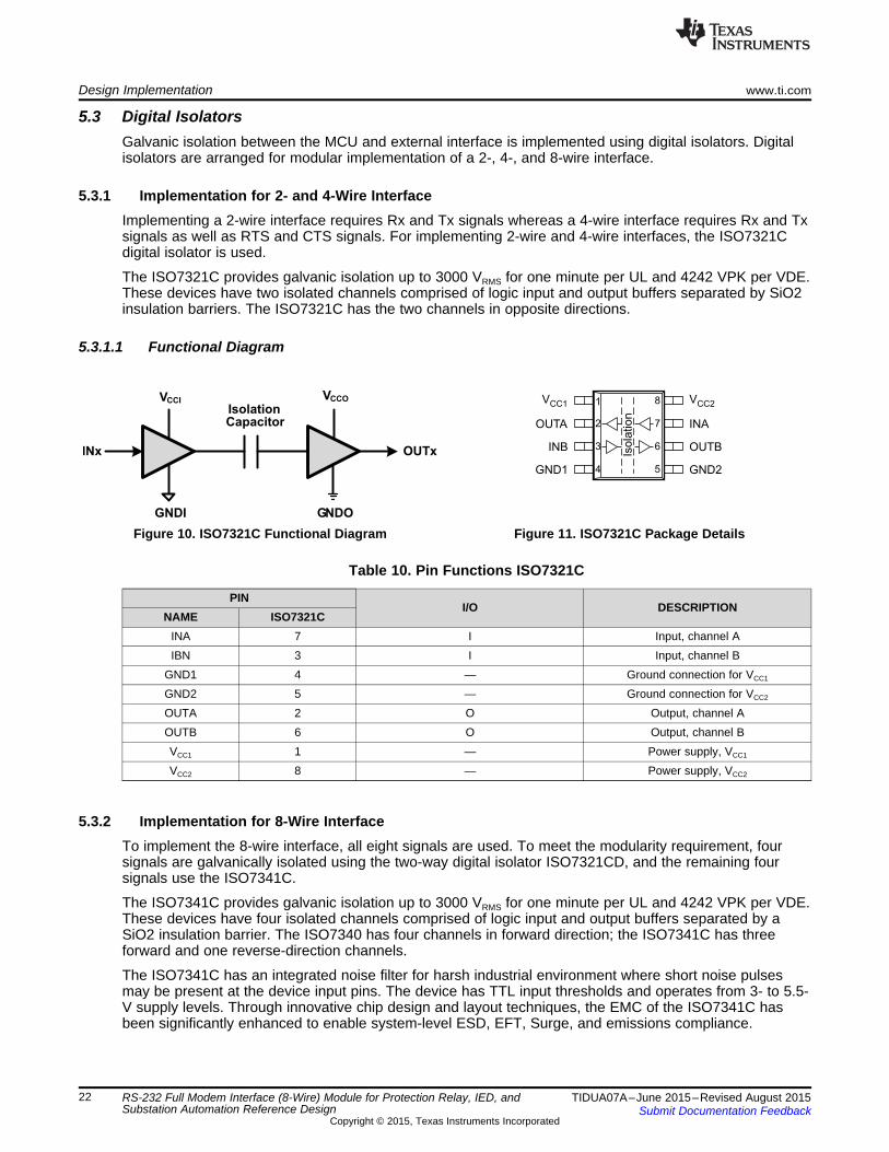
5.3 Digital IsolatorsGalvanic isolation between the MCU and external interface is implemented using digital isolators. Digitalisolators are arranged for modular implementation of a 2-, 4-, and 8-wire interface.
5.3.1 Implementation for 2- and 4-Wire InterfaceImplementing a 2-wire interface requires Rx and Tx signals whereas a 4-wire interface requires Rx and Txsignals as well as RTS and CTS signals. For implementing 2-wire and 4-wire interfaces, the ISO7321Cdigital isolator is used.
The ISO7321C provides galvanic isolation up to 3000 VRMS for one minute per UL and 4242 VPK per VDE.These devices have two isolated channels comprised of logic input and output buffers separated by SiO2insulation barriers. The ISO7321C has the two channels in opposite directions.
NAME ISO7321CINA 7 I Input, channel AIBN 3 I Input, channel B
GND1 4 — Ground connection for VCC1
GND2 5 — Ground connection for VCC2
OUTA 2 O Output, channel AOUTB 6 O Output, channel BVCC1 1 — Power supply, VCC1
VCC2 8 — Power supply, VCC2
5.3.2 Implementation for 8-Wire InterfaceTo implement the 8-wire interface, all eight signals are used. To meet the modularity requirement, foursignals are galvanically isolated using the two-way digital isolator ISO7321CD, and the remaining foursignals use the ISO7341C.
The ISO7341C provides galvanic isolation up to 3000 VRMS for one minute per UL and 4242 VPK per VDE.These devices have four isolated channels comprised of logic input and output buffers separated by aSiO2 insulation barrier. The ISO7340 has four channels in forward direction; the ISO7341C has threeforward and one reverse-direction channels.
The ISO7341C has an integrated noise filter for harsh industrial environment where short noise pulsesmay be present at the device input pins. The device has TTL input thresholds and operates from 3- to 5.5-V supply levels. Through innovative chip design and layout techniques, the EMC of the ISO7341C hasbeen significantly enhanced to enable system-level ESD, EFT, Surge, and emissions compliance.
22 RS-232 Full Modem Interface (8-Wire) Module for Protection Relay, IED, and TIDUA07A–June 2015–Revised August 2015Substation Automation Reference Design Submit Documentation Feedback
NAME ISO7341CINA 3 I Input, channel AINB 4 I Input, channel BINC 5 I Input, channel CIND 11 I Input, channel D
OUTA 14 O Output, channel AOUTB 13 O Output, channel BOUTC 12 O Output, channel COUTD 6 O Output, channel D
Output enable 1. Output pins on side-1 are enabled when EN1 is high orEN1 7 I disconnected and disabled when EN1 is low.Output enable 2. Output pins on side-2 are enabled when EN2 is high orEN2 10 I disconnected and disabled when EN2 is low.Output enable. All output pins on are enabled when EN is high or disconnected andEN — I disabled when EN is low.
VCC1 1 — Power supply, VCC1
VCC2 16 — Power supply, VCC2
GND1 2, 8 — Ground connection for VCC1
GND2 9, 15 — Ground connection for VCC2
NC — — No connect pins are floating with no internal connection.
23TIDUA07A–June 2015–Revised August 2015 RS-232 Full Modem Interface (8-Wire) Module for Protection Relay, IED, andSubstation Automation Reference DesignSubmit Documentation Feedback
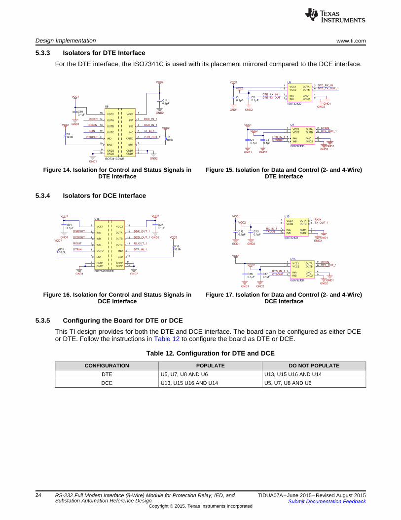
5.3.3 Isolators for DTE InterfaceFor the DTE interface, the ISO7341C is used with its placement mirrored compared to the DCE interface.
Figure 14. Isolation for Control and Status Signals in Figure 15. Isolation for Data and Control (2- and 4-Wire)DTE Interface DTE Interface
5.3.4 Isolators for DCE Interface
Figure 16. Isolation for Control and Status Signals in Figure 17. Isolation for Data and Control (2- and 4-Wire)DCE Interface DCE Interface
5.3.5 Configuring the Board for DTE or DCEThis TI design provides for both the DTE and DCE interface. The board can be configured as either DCEor DTE. Follow the instructions in Table 12 to configure the board as DTE or DCE.
Table 12. Configuration for DTE and DCE
CONFIGURATION POPULATE DO NOT POPULATEDTE U5, U7, U8 AND U6 U13, U15 U16 AND U14DCE U13, U15 U16 AND U14 U5, U7, U8 AND U6
24 RS-232 Full Modem Interface (8-Wire) Module for Protection Relay, IED, and TIDUA07A–June 2015–Revised August 2015Substation Automation Reference Design Submit Documentation Feedback
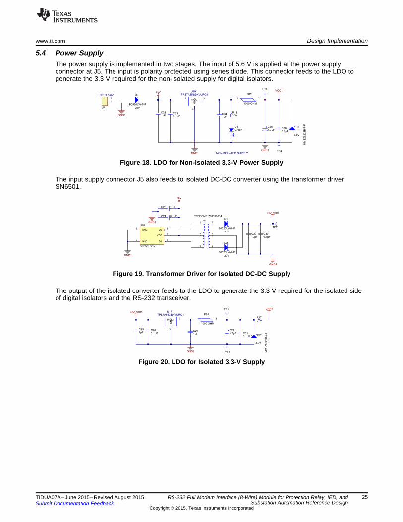
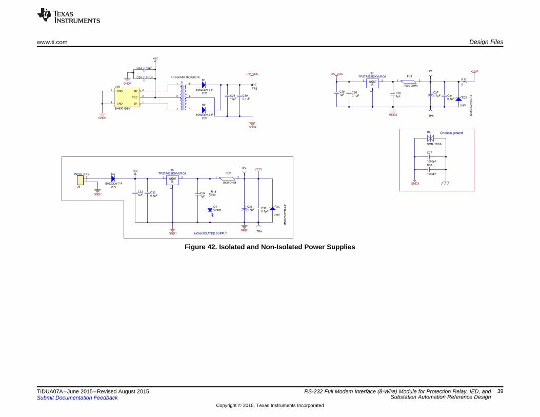
5.4 Power SupplyThe power supply is implemented in two stages. The input of 5.6 V is applied at the power supplyconnector at J5. The input is polarity protected using series diode. This connector feeds to the LDO togenerate the 3.3 V required for the non-isolated supply for digital isolators.
Figure 18. LDO for Non-Isolated 3.3-V Power Supply
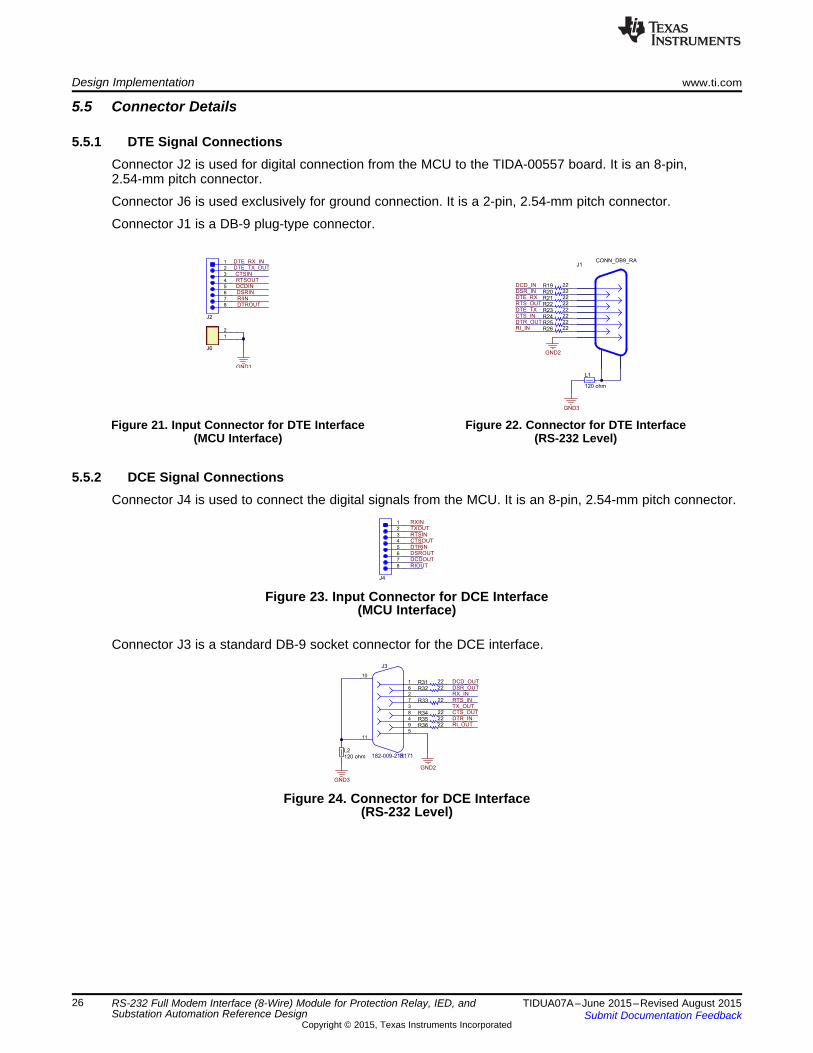
The input supply connector J5 also feeds to isolated DC-DC converter using the transformer driverSN6501.
Figure 19. Transformer Driver for Isolated DC-DC Supply
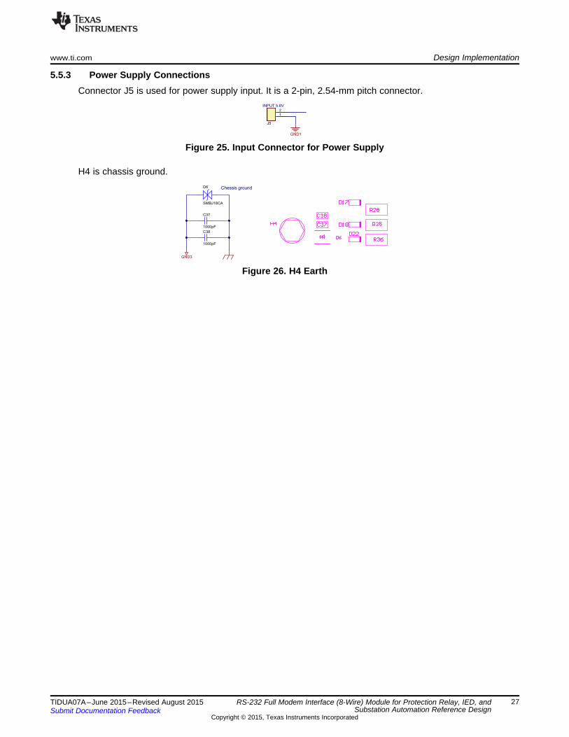
The output of the isolated converter feeds to the LDO to generate the 3.3 V required for the isolated sideof digital isolators and the RS-232 transceiver.
Figure 20. LDO for Isolated 3.3-V Supply
25TIDUA07A–June 2015–Revised August 2015 RS-232 Full Modem Interface (8-Wire) Module for Protection Relay, IED, andSubstation Automation Reference DesignSubmit Documentation Feedback
6 Getting Started: HardwareThe following section gives details of how to get started with this hardware.
6.1 Power Supply
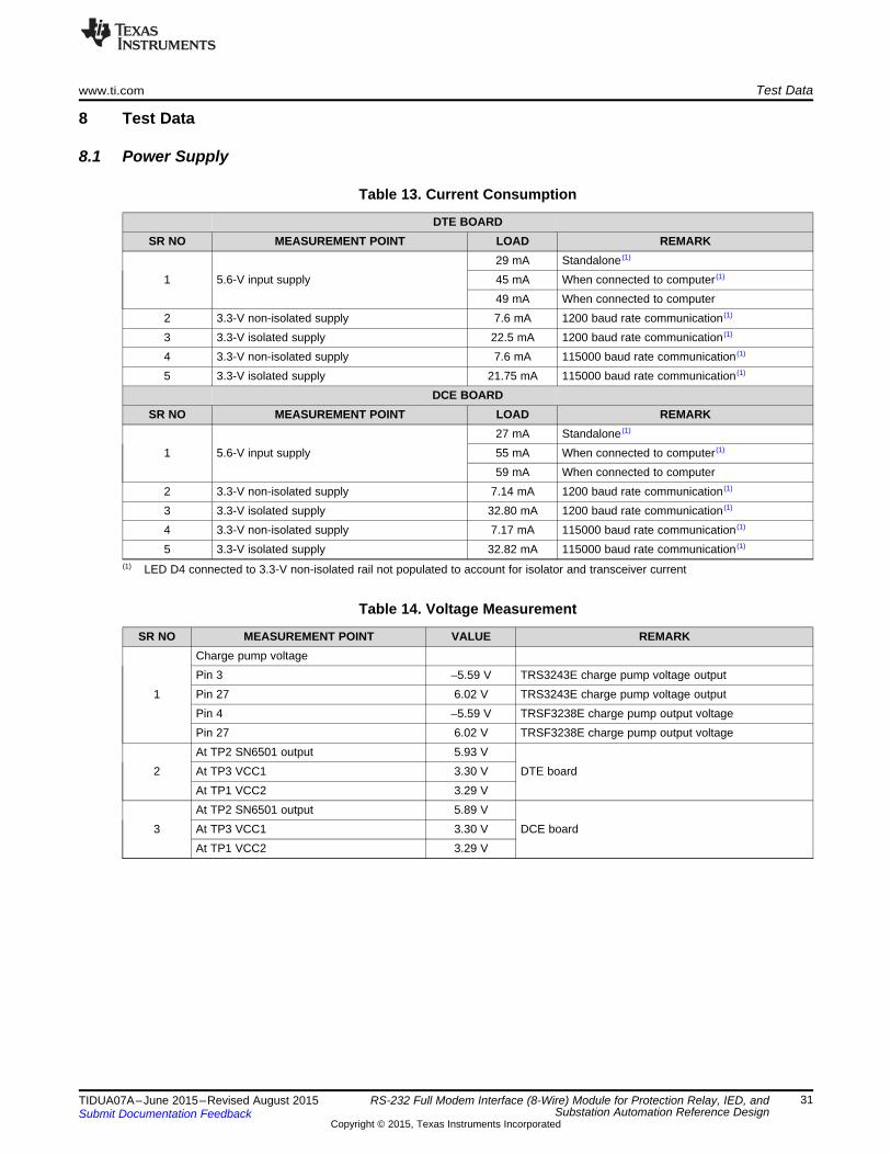
1. Connect the 5.6-V DC supply at connector J5 with a current limitation of < 200 mA.2. Measure the voltage at TP3 with respect to TP4. It should be 3.3 V.3. Measure the voltage at TP2 with respect to TP5. It should be around 6.0 V.4. Measure the voltage at TP1 with respect to TP5. It should be around 3.3 V.
Once these requirements are met, D4 should light up.
6.2 RS-232 TransceiverMeasure the following voltages:1. Measure the voltage at pin 26 of U6 (it should be 3.3 V).2. Measure the voltage at pin 27 of U6 (it should be 6.0 V).3. Measure the voltage at pin 3 of U6 (it should be –5.5-V to –6.0-V DC).
Measure the following voltages:1. Measure the voltage at pin 26 of U14 (it should be 3.3 V).2. Measure the voltage at pin 27 of U14 (it should be 6.0 V).3. Measure the voltage at pin 4 of U14 (it should be –5.5-V to –6.0-V DC).
28 RS-232 Full Modem Interface (8-Wire) Module for Protection Relay, IED, and TIDUA07A–June 2015–Revised August 2015Substation Automation Reference Design Submit Documentation Feedback
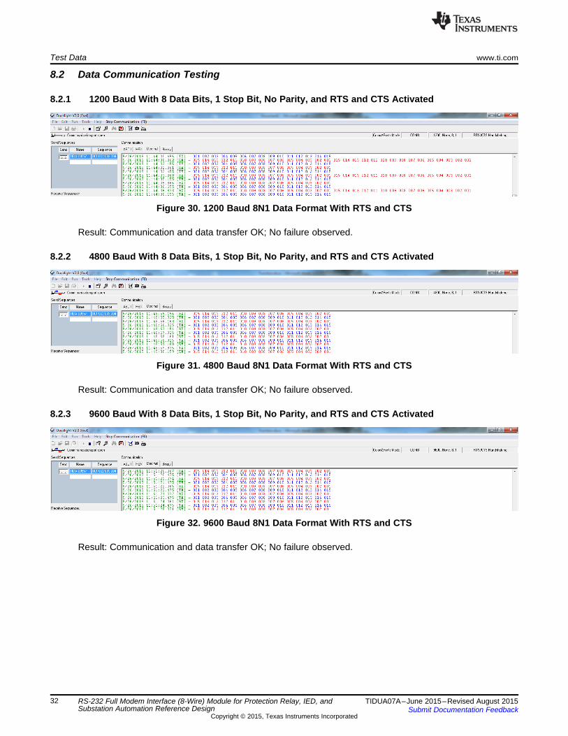
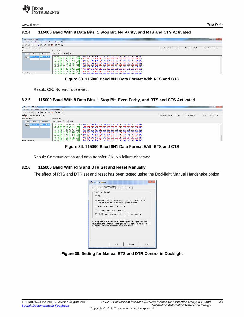
8.2.4 115000 Baud With 8 Data Bits, 1 Stop Bit, No Parity, and RTS and CTS Activated
Figure 33. 115000 Baud 8N1 Data Format With RTS and CTS
Result: OK; No error observed.
8.2.5 115000 Baud With 8 Data Bits, 1 Stop Bit, Even Parity, and RTS and CTS Activated
Figure 34. 115000 Baud 8N1 Data Format With RTS and CTS
Result: Communication and data transfer OK; No failure observed.
8.2.6 115000 Baud With RTS and DTR Set and Reset ManuallyThe effect of RTS and DTR set and reset has been tested using the Docklight Manual Handshake option.
Figure 35. Setting for Manual RTS and DTR Control in Docklight
33TIDUA07A–June 2015–Revised August 2015 RS-232 Full Modem Interface (8-Wire) Module for Protection Relay, IED, andSubstation Automation Reference DesignSubmit Documentation Feedback
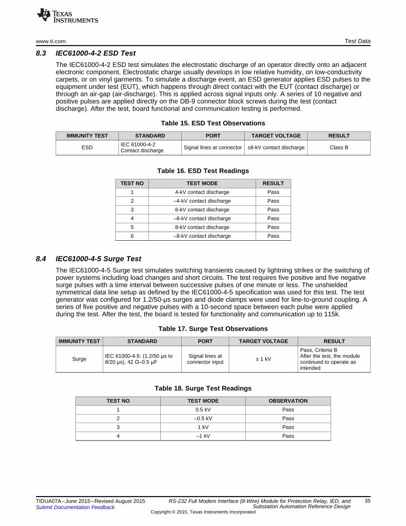
8.3 IEC61000-4-2 ESD TestThe IEC61000-4-2 ESD test simulates the electrostatic discharge of an operator directly onto an adjacentelectronic component. Electrostatic charge usually develops in low relative humidity, on low-conductivitycarpets, or on vinyl garments. To simulate a discharge event, an ESD generator applies ESD pulses to theequipment under test (EUT), which happens through direct contact with the EUT (contact discharge) orthrough an air-gap (air-discharge). This is applied across signal inputs only. A series of 10 negative andpositive pulses are applied directly on the DB-9 connector block screws during the test (contactdischarge). After the test, board functional and communication testing is performed.
Table 15. ESD Test Observations
IMMUNITY TEST STANDARD PORT TARGET VOLTAGE RESULTIEC 61000-4-2ESD Signal lines at connector ±8-kV contact discharge Class BContact discharge
Table 16. ESD Test Readings
TEST NO TEST MODE RESULT1 4-kV contact discharge Pass2 –4-kV contact discharge Pass3 6-kV contact discharge Pass4 –6-kV contact discharge Pass5 8-kV contact discharge Pass6 –8-kV contact discharge Pass
8.4 IEC61000-4-5 Surge TestThe IEC61000-4-5 Surge test simulates switching transients caused by lightning strikes or the switching ofpower systems including load changes and short circuits. The test requires five positive and five negativesurge pulses with a time interval between successive pulses of one minute or less. The unshieldedsymmetrical data line setup as defined by the IEC61000-4-5 specification was used for this test. The testgenerator was configured for 1.2/50-μs surges and diode clamps were used for line-to-ground coupling. Aseries of five positive and negative pulses with a 10-second space between each pulse were appliedduring the test. After the test, the board is tested for functionality and communication up to 115k.
Table 17. Surge Test Observations
IMMUNITY TEST STANDARD PORT TARGET VOLTAGE RESULTPass, Criteria B
IEC 61000-4-5: (1.2/50 μs to Signal lines at After the test, the moduleSurge ± 1 kV8/20 μs), 42 Ω–0.5 μF connector input continued to operate asintended
Table 18. Surge Test Readings
TEST NO TEST MODE OBSERVATION1 0.5 kV Pass2 –0.5 kV Pass3 1 kV Pass4 –1 kV Pass
35TIDUA07A–June 2015–Revised August 2015 RS-232 Full Modem Interface (8-Wire) Module for Protection Relay, IED, andSubstation Automation Reference DesignSubmit Documentation Feedback
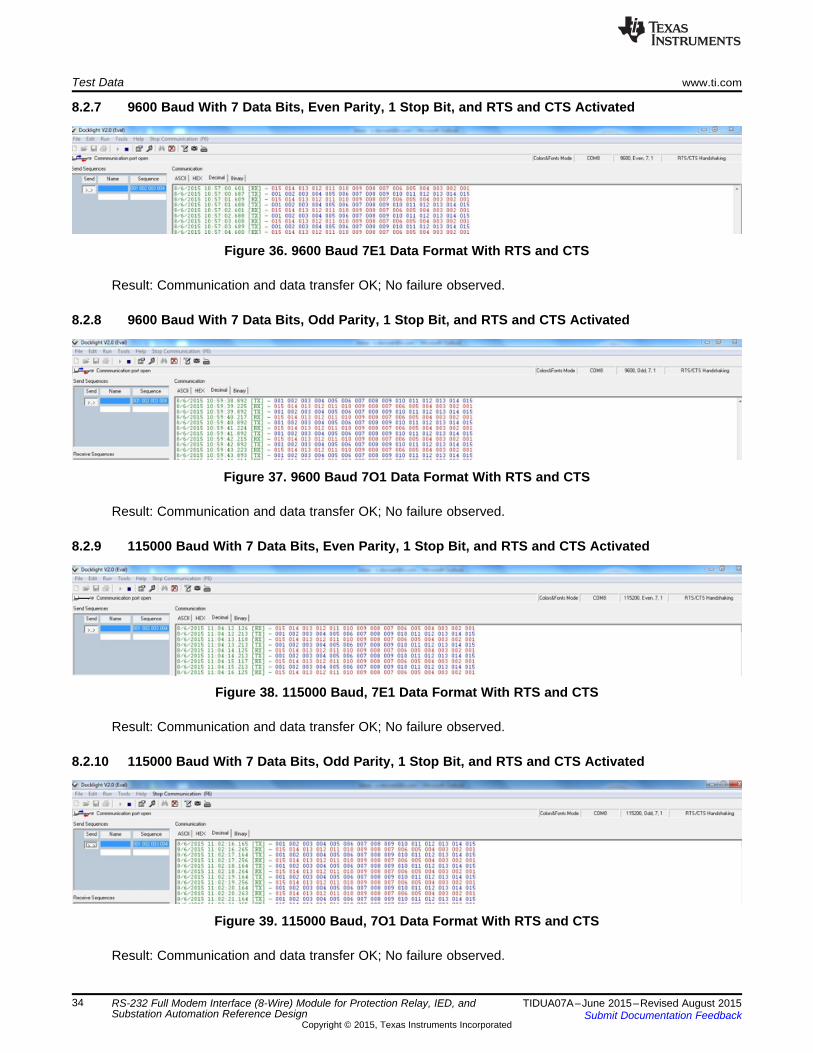
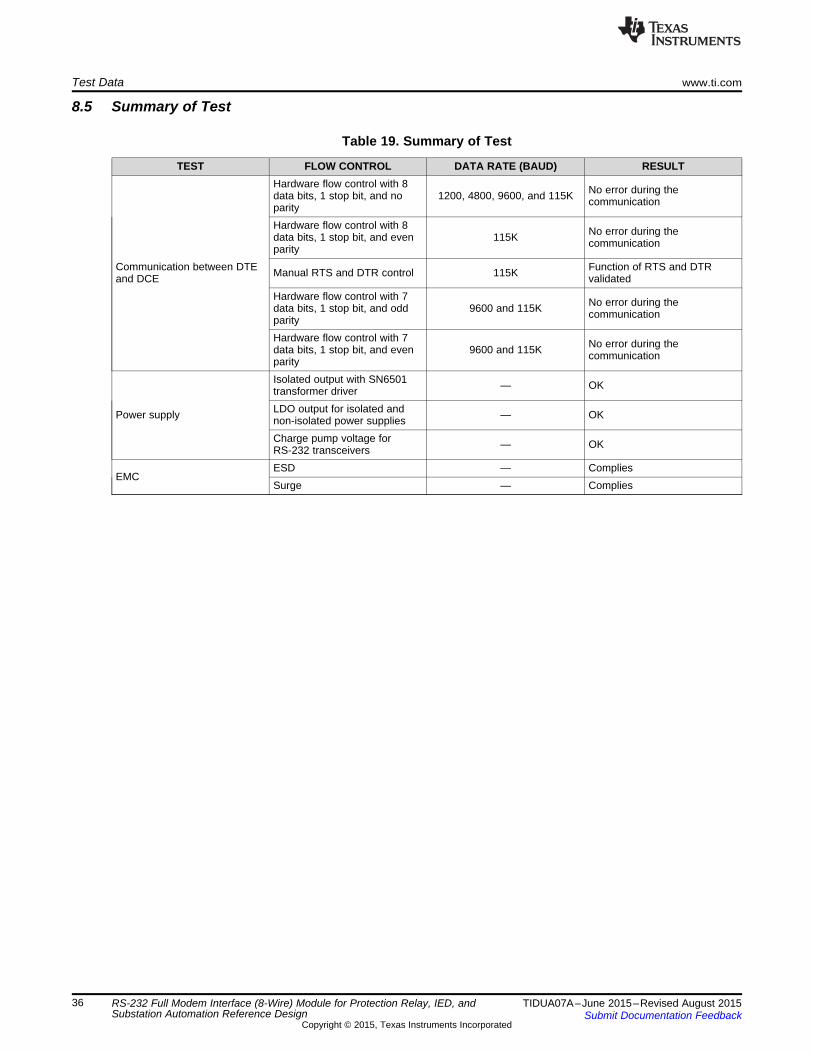
TEST FLOW CONTROL DATA RATE (BAUD) RESULTHardware flow control with 8 No error during thedata bits, 1 stop bit, and no 1200, 4800, 9600, and 115K communicationparityHardware flow control with 8 No error during thedata bits, 1 stop bit, and even 115K communicationparity
Communication between DTE Function of RTS and DTRManual RTS and DTR control 115Kand DCE validatedHardware flow control with 7 No error during thedata bits, 1 stop bit, and odd 9600 and 115K communicationparityHardware flow control with 7 No error during thedata bits, 1 stop bit, and even 9600 and 115K communicationparityIsolated output with SN6501 — OKtransformer driverLDO output for isolated andPower supply — OKnon-isolated power suppliesCharge pump voltage for — OKRS-232 transceiversESD — Complies
EMCSurge — Complies
36 RS-232 Full Modem Interface (8-Wire) Module for Protection Relay, IED, and TIDUA07A–June 2015–Revised August 2015Substation Automation Reference Design Submit Documentation Feedback
9.2 Bill of MaterialsTo download the bill of materials (BOM), see the design files at TIDA-00557.
9.3 PCB Layout Recommendations• Creepage and clearance requirements should be applied according to the specific application isolation
standards. Care should be taken to maintain these distances on the board design to ensure that themounting pads for the isolator do not reduce this distance. Creepage and clearance on the printedcircuit board become equal in certain cases. Techniques such as inserting grooves and/or ribs on theprinted circuit board are used to help increase these specifications.
• An SMD ceramic bypass capacitor of approximately 0.1 μF in value is recommended. If leadedcomponents are necessary, leads should be kept as short as possible to minimize lead inductance.
• A continuous ground plane is ideal for providing a low-impedance signal return path, as well asgenerating the lowest EMI signature by reducing phenomena such as unintended current loops.
• Should a continuous ground plane not be possible, minimize the length of the trace connecting VCCand ground.
• Isolated communication may often have to meet specified creepage and clearance criteria. Creepageand clearance requirements are determined by the end-use device specifications.
• PCB material - Standard FR-4 epoxy-glass as printed-circuit board (PCB) material is preferred forindustrial applications with speed.
• Trace Routing - Use 45° bends (chamfered corners), instead of right-angle (90°) bends. Right-anglebends increase the effective trace width, and thus the trace impedance. This creates additionalimpedance mismatch, which may lead to higher reflections.
9.3.1 Layer PlotsTo download the layer plots, see the design files at TIDA-00557.
9.4 Altium ProjectTo download the Altium project files, see the design files at TIDA-00557.
9.5 Gerber FilesTo download the Gerber files, see the design files at TIDA-00557.
9.6 Assembly DrawingsTo download the assembly rawings, see the design files at TIDA-00557.
9.7 Software FilesTo download the software files, see the design files at TIDA-00557.
40 RS-232 Full Modem Interface (8-Wire) Module for Protection Relay, IED, and TIDUA07A–June 2015–Revised August 2015Substation Automation Reference Design Submit Documentation Feedback
1. EE Herald, Online course on Embedded Systems: MODULE - 8(http://www.eeherald.com/section/design-guide/esmod8.html)
2. Lammert Bies, RS232 Specifications and standard (http://www.lammertbies.nl/comm/info/RS-232_specs.html)
3. Texas Instruments, Interface Circuits for TIA/EIA-232-F, Design Notes (SLLA037)4. Viola Systems, Towards a Smarter Grid: A Case for Using Public Wireless Networks in Smart Grid
Solutions, White Paper (http://www.pmas.in/White%20Paper%20wireless%20connection.pdf)5. Texas Instruments, 3-V TO 5.5-V MULTICHANNEL RS-232 LINE DRIVER/RECEIVER WITH ±15-kV
IEC ESD PROTECTION, TRS3234E Datasheet (SLLS789)6. Texas Instruments, 3-V TO 5.5-V MULTICHANNEL RS-232 LINE DRIVER/RECEIVER WITH ±15-kV
11 About the AuthorSUNIL DWIVEDI is a Systems Engineer at Texas Instruments where he is responsible for developingreference design solutions for the industrial segment. Sunil brings to this role his experience in high-speeddigital and analog systems design. Sunil earned his bachelor of electronics (BE) in electronics andinstrumentation engineering (BE E&I) from SGSITS, Indore, India.
41TIDUA07A–June 2015–Revised August 2015 RS-232 Full Modem Interface (8-Wire) Module for Protection Relay, IED, andSubstation Automation Reference DesignSubmit Documentation Feedback
Changes from Original (June 2015) to A Revision ......................................................................................................... Page
• Changed from the preview page ........................................................................................................ 1
NOTE: Page numbers for previous revisions may differ from page numbers in the current version.
42 Revision History TIDUA07A–June 2015–Revised August 2015Submit Documentation Feedback
Texas Instruments Incorporated ("TI") reference designs are solely intended to assist designers (“Buyers”) who are developing systems thatincorporate TI semiconductor products (also referred to herein as “components”). Buyer understands and agrees that Buyer remainsresponsible for using its independent analysis, evaluation and judgment in designing Buyer’s systems and products.TI reference designs have been created using standard laboratory conditions and engineering practices. TI has not conducted anytesting other than that specifically described in the published documentation for a particular reference design. TI may makecorrections, enhancements, improvements and other changes to its reference designs.Buyers are authorized to use TI reference designs with the TI component(s) identified in each particular reference design and to modify thereference design in the development of their end products. HOWEVER, NO OTHER LICENSE, EXPRESS OR IMPLIED, BY ESTOPPELOR OTHERWISE TO ANY OTHER TI INTELLECTUAL PROPERTY RIGHT, AND NO LICENSE TO ANY THIRD PARTY TECHNOLOGYOR INTELLECTUAL PROPERTY RIGHT, IS GRANTED HEREIN, including but not limited to any patent right, copyright, mask work right,or other intellectual property right relating to any combination, machine, or process in which TI components or services are used.Information published by TI regarding third-party products or services does not constitute a license to use such products or services, or awarranty or endorsement thereof. Use of such information may require a license from a third party under the patents or other intellectualproperty of the third party, or a license from TI under the patents or other intellectual property of TI.TI REFERENCE DESIGNS ARE PROVIDED "AS IS". TI MAKES NO WARRANTIES OR REPRESENTATIONS WITH REGARD TO THEREFERENCE DESIGNS OR USE OF THE REFERENCE DESIGNS, EXPRESS, IMPLIED OR STATUTORY, INCLUDING ACCURACY ORCOMPLETENESS. TI DISCLAIMS ANY WARRANTY OF TITLE AND ANY IMPLIED WARRANTIES OF MERCHANTABILITY, FITNESSFOR A PARTICULAR PURPOSE, QUIET ENJOYMENT, QUIET POSSESSION, AND NON-INFRINGEMENT OF ANY THIRD PARTYINTELLECTUAL PROPERTY RIGHTS WITH REGARD TO TI REFERENCE DESIGNS OR USE THEREOF. TI SHALL NOT BE LIABLEFOR AND SHALL NOT DEFEND OR INDEMNIFY BUYERS AGAINST ANY THIRD PARTY INFRINGEMENT CLAIM THAT RELATES TOOR IS BASED ON A COMBINATION OF COMPONENTS PROVIDED IN A TI REFERENCE DESIGN. IN NO EVENT SHALL TI BELIABLE FOR ANY ACTUAL, SPECIAL, INCIDENTAL, CONSEQUENTIAL OR INDIRECT DAMAGES, HOWEVER CAUSED, ON ANYTHEORY OF LIABILITY AND WHETHER OR NOT TI HAS BEEN ADVISED OF THE POSSIBILITY OF SUCH DAMAGES, ARISING INANY WAY OUT OF TI REFERENCE DESIGNS OR BUYER’S USE OF TI REFERENCE DESIGNS.TI reserves the right to make corrections, enhancements, improvements and other changes to its semiconductor products and services perJESD46, latest issue, and to discontinue any product or service per JESD48, latest issue. Buyers should obtain the latest relevantinformation before placing orders and should verify that such information is current and complete. All semiconductor products are soldsubject to TI’s terms and conditions of sale supplied at the time of order acknowledgment.TI warrants performance of its components to the specifications applicable at the time of sale, in accordance with the warranty in TI’s termsand conditions of sale of semiconductor products. Testing and other quality control techniques for TI components are used to the extent TIdeems necessary to support this warranty. Except where mandated by applicable law, testing of all parameters of each component is notnecessarily performed.TI assumes no liability for applications assistance or the design of Buyers’ products. Buyers are responsible for their products andapplications using TI components. To minimize the risks associated with Buyers’ products and applications, Buyers should provideadequate design and operating safeguards.Reproduction of significant portions of TI information in TI data books, data sheets or reference designs is permissible only if reproduction iswithout alteration and is accompanied by all associated warranties, conditions, limitations, and notices. TI is not responsible or liable forsuch altered documentation. Information of third parties may be subject to additional restrictions.Buyer acknowledges and agrees that it is solely responsible for compliance with all legal, regulatory and safety-related requirementsconcerning its products, and any use of TI components in its applications, notwithstanding any applications-related information or supportthat may be provided by TI. Buyer represents and agrees that it has all the necessary expertise to create and implement safeguards thatanticipate dangerous failures, monitor failures and their consequences, lessen the likelihood of dangerous failures and take appropriateremedial actions. Buyer will fully indemnify TI and its representatives against any damages arising out of the use of any TI components inBuyer’s safety-critical applications.In some cases, TI components may be promoted specifically to facilitate safety-related applications. With such components, TI’s goal is tohelp enable customers to design and create their own end-product solutions that meet applicable functional safety standards andrequirements. Nonetheless, such components are subject to these terms.No TI components are authorized for use in FDA Class III (or similar life-critical medical equipment) unless authorized officers of the partieshave executed an agreement specifically governing such use.Only those TI components that TI has specifically designated as military grade or “enhanced plastic” are designed and intended for use inmilitary/aerospace applications or environments. Buyer acknowledges and agrees that any military or aerospace use of TI components thathave not been so designated is solely at Buyer's risk, and Buyer is solely responsible for compliance with all legal and regulatoryrequirements in connection with such use.TI has specifically designated certain components as meeting ISO/TS16949 requirements, mainly for automotive use. In any case of use ofnon-designated products, TI will not be responsible for any failure to meet ISO/TS16949.IMPORTANT NOTICE