69
Secure Voice Signal Processing SVSP

Secure Voice Signal Processing
SVSP

8-bit Secure Signal ProcessingFinal Report
Jodie AuJosh Chong
Tam ParedesJeff Sieben
Amelia Yeoh
University of AlbertaEE 552

ii
Declaration of Original Content
The project and the contents of this report are entirely the original work of theauthors except as follows:
Figures
Figure 2.2.1 taken from reference [3]Figure 2.2.2 taken from reference [3]Figure 2.2.3 taken from reference [3]Figure 2.3.1 taken from reference [5]Figure 2.3.2 taken from reference [5]Figure 2.3.3 taken from reference [5]Table 2.3.1 taken from reference [5]
VHDL Files
clock_divider.vhd taken from reference [7]input_reader.vhd modified from reference [7]
fifo.vhd taken from reference [6]txmit.vhd modified from reference [5]
rxcver.vhd modified from reference [5]
Jodie Au: _____________________________________________
Josh Chong: _____________________________________________
Tam Paredes: _____________________________________________
Jeff Sieben: _____________________________________________
Amelia Yeoh: _____________________________________________

Table of Contents
1. Achievements........................................................................................................................11.1 ADC...................................................................................................................................21.2 Encryption/Decryption.....................................................................................................21.3 Transmitter/Receive.........................................................................................................31.4 DAC...................................................................................................................................31.5 Compression/Decompression.........................................................................................3
2. Operation...............................................................................................................................42.1 ADC...................................................................................................................................42.2 Compression/Decompression.......................................................................................142.3 Encryption/Decryption...................................................................................................152.4 Transmitter/Receive.......................................................................................................192.5 DAC.................................................................................................................................23
3.I/O Signals ............................................................................................................................264. Design Hierarchy.................................................................................................................325. FPGA Resources .................................................................................................................34
5.1 ADC.................................................................................................................................345.2 Encryption/Decryption...................................................................................................345.3 Transmitter/Receive.......................................................................................................34
6. Experimentation ..................................................................................................................406.1 Transmitter/Receive.......................................................................................................356.2 Compression/Decompression.......................................................................................35
7. Integrated Test Measurements (Not Included)...................................................................378. Research..............................................................................................................................379. References...........................................................................................................................3910. Test Case Index .................................................................................................................4012. VHDL Source Code Index..................................................................................................6313. Test Bench Index...............................................................................................................64A. Appendix : Data Sheets ......................................................................................................65

1
1. Achievements
The SafeTalk prototype has been very successful in design, simulation, and implementation.The experimentation is promising and the outlook for future versions of SafeTalk is positive. Thespeech signal has been successfully converted to a digital signal and back into an analog signal.This milestone set the tone for successes during the remainder of the project. The transmissionand receiving modules of SafeTalk were the cornerstones in the final result. A universalasynchronous receive transmitter (UART) simulated properly, and because it was asynchronous ittransmitted and received encrypted data automatically. As well, the simulations correctly indicatethat the framing and parity error checking mechanism was in place. Finally, the encryptionmodule is designed to allow for a stronger algorithm to secure speech data. The most exciting partof the encryption module is that the data is not audibly recognizable if converted to analog. Eventhough the cipher that was used is not secure by some standards, your roommate could not tellwhat you were saying to your friends on the other line.
The entire design of SafeTalk comprises of many different subsections. A lot of our objectives andgoals were achieved although we must admit that there are still a number of small sub-sectionsthat hasThe achievements obtained throughout the entire duration of our project is briefly explained in thetable below:
COMPILATIONSUCCESSFUL
SIMULATIONWAVEFORM AS
EXPECTED
CODE IMPLEMENTATION WITHHARDWARE &/OR FPGA BOARDWITH CORRECT OUTPUTS
ADC hardware √ √ √DAC hardware √ √ √ADC & DAC √ √ √
Compression x x x
Encryption Code (EC) √ √ √Encryption with ADC √ √ √Encryption withTransmission
√ √ √
Decryption Code (DC) √ √ √Decryption with DAC √ √ √Decryption withReceiver
√ √ √
Transmission Code (TC) √ √ √Receiver Code (RC) √ √ ∼TC & RC withcontroller
√ √ ∼
TC, RC, controller withFIFO buffer
√ √ ∼
TC & RC with ADC &DAC hardware
√ ∼
ADC hardware, EC, &TC
√ √ √
DAC hardware, DC, &RC
√ × √

2
1.1 ADC
The ADC design has hardware and software components. The hardware componentconsists of an analog circuit with 2 operational-amplifiers, one low pass filter, oneSample & Hold chip, and an ADC0809 chip. This circuit performs correctly whenconnected to the FLEX10K board using the function generator / microphone to generatean input signal.
The waveforms observed on the oscilloscope are as expected. Output signals are verifiedto be similar to that of the input signal. Signals like sample, SOC, EOC, and clock(of the ADC0809) were also probed on the oscilloscope to verify correctness. Theseagain match the expected values. The simulation waveforms for the various test cases areenclosed in this document.
The software component consists of two VHDL programs – input_reader.vhd &clock_divider.vhd. Both VHDL programs simulated correctly without anyglitches. Refer to the simulation waveforms enclosed in this document.
Attempts were also made to connect the ADC with the DAC. The function generator wasused as an input, because the signal it produces is much more consistent a human voiceinput. The output produced by the DAC circuits are exactly identical to that of the inputwaveform produced by the function generator except for s slight delay and amplificationin the output signal , thus confirming the fact that the analog-digital-analog conversionprocess works. Although there were some noise interference in the output waveform, thevoices transmitted were relatively audible. The input waveforms used for testing variedfrom a sinusoidal wave to a square wave to a triangular waveform, which gave a range ofdifferent inputs to test. The outputs are identical to that of the input. The clock frequencyused for testing purposes was approximately 840kHz (divisor value for clock_divider.vhdis 15). When a microphone was used as an input, voices can be heard through thespeaker. Although there was some noise interference, the sound quality was quitesatisfactory. The ADC module functions correctly.
1.2 Encryption/Decryption
The stream cipher operates correctly in both the encryption and decryption stages. Testswere performed on the FPGA to ensure its correct operation. The parallel-to-serial andserial-to-parallel converters were also successfully interfaced with the input and output,respectively, of the stream cipher. Furthermore, the encryption VHDL entity wassuccessfully connected to the ADC entity. The tests performed with the ADC hardwareand the FPGA show promising results. The outputs of the encryptor are non-periodicsquare waves that correspond to the binary logic 0’s and l’s that are the expected outputsof the encryptor. The decryption VHDL entity was also successfully integrated with theDAC hardware. The tests performed show that this compound entity properly decryptsdata.
However, the attempts to integrate these compound entities (i.e. ADC/encryptor anddecryptor/DAC) with the transmitter and receiver, respectively, have not been successful.As well, integration of the compound entities with the DSP controller is not currentlysuccessful.
It must be noted that the stream cipher in this project is based on linear shift registers.This type of implementation for the stream cipher is not considered strong security. The
3
reason for choosing this implementation is that it is simpler than most other streamciphers or block ciphers. So it is fast to implement and is more realistic for the scope ofour project. It allowed us to complete the encryption/decryption stages and to test it withthe rest of the system. The limitations of this cipher are noted, and as such, the cipherentity was built as a completely separate module, so it can more easily be replaced by amore complex and more secure cipher if time permitted. The success of completing thissimple cipher used can be regarded as a successful step in fully implementing SafeTalk
1.3 Transmitter/Receive
The UART is used in the transmission of the digital data, which is obtained from theDAC and encrypted in the FPGA. The original files obtained from QuickLogic partiallyworked. With some experimentation and testing both the transmitter and receivermodules were modified to transmit and receive properly in the simulations. The problemarises when the code is uploaded to the FPGA and executed. For reasons that are notdetermined the correct reception of data did not occur correctly in spite of the resultsobtained from the simulations. Framing errors and parity errors occurred frequently. Inthe end we were able to get the UART to transmit and receive without errors. The propertransmission/reception of the data was achieved after careful testing. The modificationswere made to allow the proper transmission.
1.4 DAC
All of tests performed by the DAC shows that the DAC works successfully. The DACaccepts an 8-bit digital data and converts it to an analog signal. Using three test cases, weare able to conclude that the DAC works as expected. Using either the manual switchesfrom the UP1 board or a counter written in VHDL code as the input, the DACsuccessfully converts both digital signals to analog waveforms.
Finally, testing the DAC with the ADC verifies the all conclusions made for the DAC.The output signal is identical to the input signal (microphone/function generator) exceptfor some propagation delay and signal amplification. The design and use of the DAC isverified as a completed step towards the success of SafeTalk.
1.5 Compression/Decompression
When a speech signal is compressed the redundancies in information are removedbecause they are not needed to reconstruct the signal. That way only relevant informationis utilized. The conversion of an audio signal from analog to digital is simple, however,the data that results in the conversion to digital is large compared to the data needed toreconstruct it and convert it back to analog. As a result a large speed modem—64Kbps—would be required to send all the information. This modem speed can not be obtainedwith the resources available therefore compression is needed.
The members did not have any basis as to how compression worked, and thereforeresearch started at the search engines on the Internet. The outcome of the research is thatknowledge is gained in the areas of speech characteristics and speech compression. Thecompression algorithm is an amateur design that reduces the number of bits to representthe digital speech signal. Samples are converted at 840KHz, so to keep the massiveamounts of data passing through to the UART, 1 in every 8 samples is removed. Thisprovides an effective sample of 8KHz. The design and simulation of the compression isdocumented in this document.

4
2. Operation
2.1 ADC
The analog-to-digital converter is broken up into the hardware design and the softwaredesign.
For the hardware design, the circuit is divided into 5 sub-sections:1. Audio Condenser Microphone (AM 242)2. Analog Operational Amplifiers (LM324)3. Low Pass Filter (LF351)4. Sample and Hold (SMP11)5. A/D converter (ADC0809)
2.1.1SafeTalk uses a condenser microphone with an internal resistance of approximately 2k.It is a NCAT (Noise Canceling and Amplification Technology) microphone for accuratevoice input. According to the specification sheet, the sensitivity of the microphone is –67dB/uBar, -47dBV/Pascal ± 4dB. The frequency response of the microphone rangesfrom 100-16,000Hz.
2.1.2The microphone signal amplification is done in two stages with a pre-amplifier and anactual amplifier. The breakdown of this sub-section into the two amplifiers is done inorder to avoid oscillations and non-ideal operations of the op-amp at very high gainconfigurations. Both amplifier stages are built using an LM324 (Figures 2.1.1, 2.1.2)single-ended op-amp. The LM324 series DIP consists of four independent, high-gain,internally frequency compensated operational amplifiers that are designed specifically tooperate from a single power over a wide range of voltages. For our design, a single powersupply set at 5V DC is used to drive the amplifier system. Note that doing this doesindeed limit the positive output to 4.2V, this limitation can be rectified in the A/Dsection.

5
Figure 2.1.1: Pre-Amplifier Schematic
The pre-amplification (Figure 2.1.1) stage provides the main source of gain for theamplifier. The op-amp configuration used here is an inverting single-ended amplifier.The reason the chip is connected to a ±12V power supply instead of a +5V and groundsignal is to account for the clipping that occurred in the outputs of the amplifier. Both thecapacitors used here are of values 10uF and they provide DC blocking and a signalground. The gain for this amplifier is given by the formula (110k/250) = 440. Note thatthe gain value here is theoretical and practical results may differ.
2.1.3
Figure 2.1.2: AmplifierSchematic
LM
32
4
250
Ccouple10uF
110k
110k
110k
4.7k
Mic
rophone
Ground
+12V
-12V
Vcc = 5V
10uF
10k
Vout
LM32
4
Rvar
Ccouple10uF
110k
110k
110k
4.7k
Ground
+12V
-12V
Vcc
frompre-amp

6
The design for the main amplifier stage (Figure 2.1.2) is very similar to that of the pre-amplifier stage. However, the only difference is that the 250Ω resistor is replaced with a1-10kΩ potentiometer that provides the user with the flexibility to adjust the microphonesensitivity. The reason we are using +12V and –12V for the power supplies of the chipinstead of +5V and ground in order to achieve a higher voltage range and to avoidclipping in the waveforms.
2.1.4
Figure 2.1.3: Low Pass Filter Schematic
A low pass filter design is added to the ADC design to reduce noise interference. A lowpass filter allows all frequencies below a certain point, known as the cutoff frequency, topass without attenuation while suppressing all frequencies above the cutoff. The cutofffrequency is determined by the values of the capacitors C1 and C2 and resistor R1 andR2. C1 and C2 are equal in value, as are R1 and R2. The cutoff frequency is determinedby the following formula:
Cutoff = 1
2πRC
The cutoff frequency we are using is 4kHz (since typical bandwidth of voice signals isapproximately 3kHz). Therefore, rearranging the formula above gives
R4 = 1
(cutoff)(C)(2π) = 1
(4kHz)(10uF)(2π) = 3.98kΩ
The gain of this filter is equal to R4 divided by R3. The gain for this filter is 3.9kΩ/ 39Ω= 100 where R4 = 3.9 kΩ and R3 = 39Ω. R1 = R2 = 39Ω. The output at the cutofffrequency is equal to 0.707 of this circuit’s maximum output.
LF 3
51
Outputs toS&H chip
+12V
-12V
R4
C2
R2
C1R1
Input to filter comingfrom amplifier
4
6
7
39
39
10uF
3.9k
10uF
+
-R339

7
Table 2.1.1: LF 351 Pin Connections
Pin Number onLF351
Signal Name Connected to Reason
4 V+ +12V (Active High) In order for chip to function efficiently7 V- -12V In order for chip to function efficiently2 Input- Input of filter Transmit data3 Input+ Input for filter Transmit data6 Output SMP11 chip input
(Pin 2- SMP11)In order to transmit the appropriatesignals for functionality
2.1.5
Figure 2.1.4: Sample and Hold Block Schematic
The sample and hold chip (SMP11) samples rapidly changing inputs (voice waveform) inorder to provide a stable value for the A/D converter over a period of time. See Figure2.1.4 for the schematic circuit.
The sample and hold (S&H) chip provides the A/D converter with a stable value over acertain period of time in order for the A/D chip to perform the conversion efficiently. Theneed for the S&H chip is essential in order to provide the A/D chip with a constant valueinstead of a rapidly changing input—such as the waveform generated from human voices.
SM
P11
Ground
-12V
+12V
Vcc = 5V
Sample
output from the filter
to the input of theA/D chip

8
From the specification sheets, the sample time takes about 1.5us and the hold time isapproximately 100us. It is important to note that the S&H chip requires at least (12V tooperate efficiently although this is not explicitly stated in the specification sheet of thechip. For the value of Chold, the typical value of 0.005uF is used. This allows for asample time of 0.75us (90% input) on a signal and a maximum of 5V swing. To allowimperfections of the chip or the circuit, the S&H time is chosen to be 1.5us.
The maximum voltage for the A/D chip is Vcc + 0.3V. Since the S&H chip can output 12volts at full swing, two protection diodes are added onto the output of the S&H chip asshown in the figure above to clamp the output between Vcc + Vdiode and Gnd – Vdiode.
The S&H chip requires that the signal be low for hold and high for sample. The durationof time when the signal is low (hold=100us) is much longer than the duration of timewhen signal is high (sample=1.5us). Control of it is done through the VHDL codeentitled input_reader.vhd.
Some important connections for the SMP11 chip are shown in Table 2.1.2.
Table 2.1.2: SMP11 Pin Connections
Pin Numberon SMP11
Signal Name Connected to Reason
9 V+ 5V (Active High) In order for chip to functionefficiently
5 V- Ground In order for chip to functionefficiently
2 Input Output of filter(Pin 6 – LF351)
Transmit data
7 Output Input, IN0 for ADC0809 Transmit data14 Sample FLEX10K board In order to receive the appropriate
signals for functionality11 Hold Capacitor 0.005uF capacitor Chip Requirement
2.1.6
Figure 2.1.5: A/D Converter
AD
C0
80
9
Data
EOC
SOC
Clock
coming fromoutput
of SMP11

9
For the A/D conversion, we use the data acquisition component (ADC0809) with an 8 bitanalog-to-digital converter and an 8-channel multiplexer. The 8-bit converter usessuccessive approximation as the conversion technique. The advantage of this chip is thatthe 8-channel multiplexer can access any of 8-single-ended analog signals. However, forour design purposes, we are only using one analog channel input, IN0.The input/outputsof the chip are as in Table 2.1.3.
Some important facts about the ADC809 signals to familiarize with beforeimplementation:
CLOCK:According to the specification sheets for this chip, the input clock can be within the rangeof 10kHz to 1280 kHz with the typical frequency of 640kHz. For our design, we have setthe input clock frequency to be approximately 840kHz thus giving us the divisor value(clock_divider.vhd) of approximately (25.175MHz / (2 * 840kHz) = 15. This frequencyvalue is chosen so that it may be compatible with the clock frequency of that of thedigital-to-analog converter.
Note that the clock entering the ADC0809 is actually the slow_clock generated fromthe program clock_divider.vhd and it is not the actual (central) clock. The reason theslow_clock is used instead of the main clock generated by the main control (FPGA),is to enable the ADC0809 and the SMP11 chips to function efficiently (chip limitations).The slow_clock signal generated by clock_divider.vhd is a factor of (2 * divisor)slower than the main clock. The slow_clock is also falling-edge triggered as oppose tothat of the main clock that is rising edge triggered.
SOC:With the SOC signal, the duration of time when the signal is high is shorter than thatwhen the signal is low (conversion process takes approximately 100us). The signal stayshigh for one slow_clock cycle. The conversion of the analog signal to a digital signalbegins as soon as the SOC signal drops to a zero from a one.
EOC:At the end of conversion (EOC) the EOC signal goes to a zero. When the conversionprocess is taking place, the EOC signal remains at a one. The state machine remains atstate2 (in_conv) as long as the EOC signal is high. Note also that the outputs of the dataregister are updated one clock cycle before the rising edge of the EOC.
CONVERSION TIME:It takes 100us for the chip to convert a signal from analog to digital for a 840kHzfrequency clock.
Some important connections for the ADC0809 chip are as follows:

10
Table 2.1.3: ADC0809 Pin Connections
Pin Numberon ADC0809
Signal Name Connected to Reason
11 Vcc 5V (Active High) In order for chip to functionefficiently
12 VREF(+) 5V (Active High) In order for chip to functionefficiently
16 VREF(-) Ground In order for chip to functionefficiently
13 Gnd Ground In order for chip to functionefficiently
26 IN0 Analog Input(Microphone /
Function Generator)6 SOC FLEX10K Board Programming Needs7 EOC FLEX10K Board Programming Needs10 Clock FLEX10K Board To connect to slow_clock
generated by clock_divider.vhd9 Output Enable 5V (Active High) Outputs fed directly into the
FPGA and not used in the busconfiguration
25, 24, 23 Address Lines 000 IN0 is used as the input channel22 Address Latch
Enable5V (Active High) The select lines do not vary

11
Figure 2.1.6: Schematic of Complete ADC
SM
P11
AD
C08
09
LM32
4
250k
Ccouple10uF
110k
110k
110k
LM32
4
Rvar
Ccouple10uF
110k
110k
110k
4.7k
4.7k
Mic
roph
one
Ground
-12V
+12V
+12V
+12V
-12V-12V
Data
EOC
SOC
Clock
Vcc = 5V
Sample
Vcc = 5V
10uF10uF
10k
LF
351
Outputs toS&H chip
+12V
-12V
R4
C2
R2
C1R1
Input to filter comingfrom amplifier
4
6
7
39
39
10uF
3.9k
10uF
+
-
12
The software section of this A/D basically consists of 2 VHDL programs:1. clock_divider.vhd2. input_reader.vhd
The purpose of clock_divider.vhd is to decrease the speed of the central clock by a factorof (2 * divisor). The inputs for this program are the main clock and reset. The outputconsists of the slow_clock signal. The slow_clock signal is generated by the clockand provides the ADC0809 and the SMP11 chips with the appropriate clock timing tofunction efficiently.
The input_reader.vhd is program consists of a finite state machine that controls theperformance of the A/D chip. The design of the state machine is implemented in thefollowing states. See Figure 2.1.7 for the state machine.
At the first state, sample_conv, the data is taken in and sampled for 1.5us andheld for 100us. During sampling, the signal will be high and at hold, the samplesignal will drop to low.
At start_conv, the whole conversion process begins. Sample is set to zeroto hold the data while the SOC signal is set to one; the chip must hold the data ina stable value before conversion starts. Note that conversion starts at the fallingedge of the SOC signal. The SOC signal remains at one only for one completeperiod of slow_clock and when the signal drops to zero, that is when theconversion process will start. Recall the slow_clock is falling-edgetriggered, therefore when the slow_clock signal goes high, the SOC signalgoes high. When SOC goes to the value of zero, the SOC signal drops back tozero as well.
At in_conv, the conversion is taking place. SOC signal is set back to one. Recallagain the EOC signal transitions to 1 when the conversion ends. If EOC is zero,state remains in state in_conv. Otherwise, state proceeds on to end_convstate.
At the next falling edge of the slow_clock, the state proceeds fromend_conv to read_conv. Here bits is assigned to the dummy variable,hold_out and sample is set back to one. Finally, at the next falling edge ofslow_clock, state goes back to sample_conv..
Now, the entire cycle repeats itself.

13
Figure 2.1.7: FSM Transition Diagram for input_reader.vhd
sample_conv
start_conv
in_convend_conv
read_conv
EOC='1'
EOC='0'
sample <= '1'
sample <= '0'SOC <= '1'
SOC <= '1'
hold_out <= bitssample <= '1'

14
2.2 Compression/Decompression
The method used to compress the digital signal removes selected samples from the original signal.The basis of the compression scheme is the Nyquist Theorem that states a signal can besuccessfully recreated if 2 samples per period are taken. The sampling rate of the ADC is about840KHz, and for the purpose of this project this rate is too high. Please refer to the ADC detailsfor why 840KHz was chosen. The sample rate that Nyquist suggests is around 6-8KHz whichmeans that several hundred thousand samples will be removed.
The way that the compressor works is the digital input is received and down sampled for thebenefit of data transfer. As mentioned in earlier documents an (8 KHz sample rate) X (8 bits persample) is 64000 Bits per second. This is impossible over the phone line, so we need to reducethis somehow. The actual sampleing rate is somewhere around 840KHz so every 840,000 samplesone 8-bit sample is allowed to pass through. This is fine for the quality of the signal at the outputof this application because we are not aiming for quality we are aming for security. With this inmind the compressor can simply remove 840KHz – 4KHz = 836KHz sample from the signal.
The enable input must be high for the compressor to state doing anything. Once this is high thecompressor begins to check for valid data. If the controller lets the compressor know that there isa problem with the data then this is another sign that the compressor will stop working.
The last two flags are directly related to the valid out signal in that if either of these 2 signals areclear (low) then the compressor will allow the valid out signal to be low as well. This is to preventthe controller from getting ahead of itself and encrypting data that is not available.
The main controller controls the active high enable input. This controls whether the compressor ison or not. The valid_in flag is an input that comes from the controller to tell the compressor if thedata is good or not. If the data is good then the compressor compresses, and vice versa. Valid inis active high. The valid_out flag is an output that the compression stage sets. When a problemoccurs — i.e. if the input is not valid — then valid_out flag is set. Valid out is active high. Theinput signal is an 8-bit vector that comes in from the ADC. When enable is high and the data isgood the 8 bits are allowed into the compression stage and compression takes place. The output ofthe compression stage is an 8-bit vector as well. This vector holds the sample that is sent to theencryption stage.
The decompressor works just the opposite of the compressor. The signal arrives from thedecryption stage and then it is held in a register for a about 836KHz of the input/ADC clock cycle.Much like the ADC, the decompressor takes a sample and holds it until the next sample arrives atits input.
The decompression component has the same IO as the compression component although it isimplemented for decompression. The main controller controls the active high enable input. Likethe compression this tells the decompressor whether or not to decompress. The valid in flagis an input that the main controller uses to let the decompressor know that decompression shouldbe done. The valid out flag is set or cleared by the decompressor when data is not good. Theinput signal is an 8-bit digitized-decompressed audio signal that comes from the decryption stageof the application. The output signal is also an 8-bit decompressed signal that is passed onto theDAC for conversion back to audio.

15
Figure 2.2.1: Compressor/Decompressor Block Diagram
2.3 Encryption/Decryption
For the encryption stage, a stream cipher is used since stream ciphers are more suitablefor hardware implementation and real-time systems where bits of data are receivedserially—as in the case of SafeTalk.
Stream ciphers convert plaintext to ciphertext one bit at a time. The stream cipherimplementation that we use is the XOR algorithm. Refer to Figure 2.2.1. In thisimplementation, the keystream generator outputs a stream of bits: k1, k2, k3, . . ., ki. Thenthis keystream is XORed with a stream of plaintext bits (p1, p2, p3, . . ., pi) to produce thestream of ciphertext bits. This operation is described by the formula: ci = pi ⊕ ki
To recover the plaintext bits at the decryption end, the ciphertext bits are XORed with anidentical keystream. This operation is described by: pi = ci ⊕ ki.
Figure 2.3.1: XOR Stream Cipher [3]
As shown in the diagram above, a keystream generator is needed. We use a keystreamgenerator based on linear feedback shift registers (LFSRs).
clk
Valid_in
enable
Valid_out
Compressor
Input (8bit)
Output (8-bit)

16
The feedback shift register is made up of two parts: a shift register and a feedbackfunction. The shift register is initialized with n bits (called the key), and each time akeystream bit is required, all of the bits in the register are shifted 1 bit to the right. So theleast significant bit is the output bit. The new left-most bit is computed as the XOR ofcertain bits in the register. This arrangement can potentially produce a 2n-1 bit-longpseudo-random sequence (referred to as the period) before repeating. To make thismaximal-period LFSR, the polynomial formed from the tap sequence (bits that areXORed together) plus the constant 1 must be a primitive polynomial (irreduciblepolynomial that divides x2^(n-1)+1, but not xd+1 for any d that divides 2n-1) mod 2. Thedegree of the polynomial is the length of the shift register.
Our implementation uses an 8-bit register with the primitive modulo 2 polynomialx8+x4+x3+x2+1. Therefore, the tap sequence consists of bit 8, bit 4, bit 3, and bit 2. ByXORing these bits together, the resultant LFSR will be maximal length, so it will cyclethrough 28-1 values before repeating. Refer to Figure 2.2.2 below. Two other shiftregisters of length 11 bits and 13 bits are used as well. The primitive polynomialsmodulo 2 are x11+x2+1 and x13+x4+x3+x1+1, respectively.
Figure 2.3.2: 8-bit Long Maximal-Length LFSR [3]
By combining LFSRs of different lengths (i.e. different feedback polynomials), akeystream generator is made. To create a maximal length generator, the lengths of theconstituent LFSRs must be relatively prime, and all of the feedback polynomials must beprimitive modulo 2. Each time a keystream bit is required, the LFSRs are shift once andan output bit is produced as a function of the output bits of each LFSR.
The keystream generator we use is the Geffe Generator. This keystream generator usesthree LFSRs combined in a nonlinear manner. Refer to Figure 2.2.3 below. Two of theLFSRs are inputs into a multiplexer, and the third LFSR controls the output of themultiplexer. Suppose a1, a2, and a3 are the outputs of the three LFSRs, then the output ofthe Geffe generator is the following:
b = (a1 ^ a2) ⊕ ((~a1) ^ a3) where ^ represents “AND” ⊕ represents “XOR” ~ represents “NOT”
The period of this combination keystream generator is the least common multiple of theperiods of the three generators:
n = n1 * n2 * n3
= 13 * 11 * 8 = 1144
b8 b7 b6 b5 b4 b3 b2 b1
Output Bit

17
Figure 2.3.3: Geffe GeneratorBlock Diagram [3]
This keystream generator is used at both ends – encryption and decryption.
Considering the encryption end, there are two inputs to this stage: the data to beencrypted and a clock. The data to be encrypted comes from the serial output of theprevious stage. Likewise, the output from this stage is a serial output consisting of theencrypted data or ciphertext. The opposite operations occur at the decryption end.Again, there are two inputs: the encrypted data and a clock. The encrypted data isreceived serially from the previous stage. The output of the decryption section is thedecrypted data (i.e. original message).
The stream cipher takes inputs serially and sends outputs serially. However, to interfacewith the other stages an 8-bit parallel-to-serial converter is required at the input and aserial-to-parallel 8-bit converter is need at the output. When interfacing the stream cipherwith the other stages, timing as well as incoming and outgoing signals are issues thatmust be acknowledged. To properly account for these factors, the encryption anddecryption stages are considered two completely different entities, whereas before, thestream cipher designed could be used for either end without making any modifications.
The encryption stage is integrated with the analog-to-digital converter. The decryptionstage is integrated with the digital-to-analog converter. There is still a similarity betweenthe two compound entities. Both have an 8-bit shift register to convert an 8-bit parallelinput to a serial stream. The shift register works in the following manner:
i. The shift register remains in the initial (reset) stage until a data valid signal isreceived from the previous stage.
ii. When a data valid signal is received, the current 8-bit parallel input is stored intothe shift register.
iii. For 8 clock cycles after receiving the data valid signal, the bits in the register areshifted such that the least significant bit (LSB) is output. During this time, thedata valid out signal is asserted and output from the decryption-DAC compoundentity.
iv. After the 8 clock cycles, the output is no longer valid, so the data valid signal isdeasserted.
2-to-1Multiplexer
Select
LFSR-2
LFSR-3
b(t)
LFSR-1

18
This serial stream is then put through the stream cipher to be encrypted or decrypted.After decryption, the output data is changed from a serial stream to an 8-bit paralleloutput using a serial-to-parallel converter. This converter is basically a Moore finite statemachine that waits for 8 valid bits (that should be received in 8 consecutive clock cycles),and then outputs these 8 bits in parallel on the next clock cycle. The finite state machinetransition diagram is shown below.
Figure 2.3.4: s_to_p_data_conv FSM Transition Diagram
read1
wait_v
read2
send
read3
read4read5
read6
read7
valid = 0
reset = 1
rising_edge(clock),valid = 1
rising_edge(clock)
rising_edge(clock)
rising_edge(clock)
rising_edge(clock)
rising_edge(clock)
rising_edge(clock)
rising_edge(clock)
rising_edge(clock),valid = 1
valid = 0

19
The difference is that the ADC/encryption compound entity has an additionalcomponent—the ADC input reader. The way the input reader works is described inSection 2.1. There is one modification made to this component. An extra output signal,valid_out, is added to indicate to the encryption entity when the data being outputfrom the ADC is valid.
Using an LFSR-based stream cipher is not considered strong encryption. The majordownfall is that the key is hard-coded into the LFSRs, so the initial state of the encryptionstage is always the same. The reason for its use in this project is because it is easy andfast to implement. The main concern is to get a working prototype of the SafeTalksystem, even if it is a much simpler version of the one proposed. Once this isaccomplished, other features such as a stronger encryption algorithm can beimplemented. Ideally, a more complicated stream cipher, such as RC4, or even a blockcipher, such as DES, would be implemented.
2.4 Transmitter/Receive
For the transmission stage the use of the UART can be confusing at first but is ratherstraightforward once an understanding of the UART is acquired. The UART is theinterface between the modem and the DSP data to be transmitted/received.
This implementation of this UART transmits in blocks of 11 bits; 1 leading low start bit,1 trailing high stop bit, 1 parity bit and 8 data bits. The UART data format is shown inFigure 2.4.1.
Figure 2.4.1: UART data format [5]
The transmit and receive line of the UART are held high while notransmission/reception is taking place. In the transmission of a sequence the active lowstart bit indicates to the receiving UART that a new sequence of data is on its way. Thiscauses the receiving UART to take the next 8 bits as the transmitted data and the bit afterthat as the parity of these 8 data-bits. Lastly, a high stop bit is used to indicate the end ofa block. The parity can be set as even or odd and is used to indicate whether or not therehas been an error in the received data bits.
Note that errors can still occur even if the parity bit indicates no parity errors. Forexample, if the transmitted sequence is "11110000" and the parity is set as even, theparity bit that would be transmitted with the sequence would be '0'. If the receivedsequence is "11101000", the calculated parity of this sequence also equals the transmittedparity bit of '0', thereby fooling the receiving UART into thinking that there were noerrors in transmission. To test the UART please see Section 8.
20
Note: The data is transmitted LSB first. Therefore, if "10101010" is the data to betransmitted, the transmitted/received data appears as "01010101". The wholesequence would therefore be transmitted/received in this order: "00101010101"for even parity, and "00101010110" for odd parity.
The UART module is composed of 2 modules: the transmitter (Figure 2.3.2) and thereceiver (Figure 2.3.3). The operation of these two modules is not discussed here (withthe exception of the baud rate clock generator), as it is not required to be able to use theUART module. For further information concerning this, refer to the UART App Notes[1] or the respective VHDL code (Appendix E).
Figure 2.4.2: Transmit module [5] Figure 2.4.3: Receive module [5]
In order to use the UART you need to know what baud rate you want to transmit at. Thetransmitter and receiver modules have been designed with a clock divider inside, whichruns 16 times slower than the clock signal sent to it. Therefore, there should be a clockdivider running at 16 times the baud rate driving the UART modules.
If for example, you want to transmit at 33.6 kbps and the FPGA board runs at 25.175MHz then:
Baud rate x 16 = 33600 x 16 = 537600Clock division ratio = 25175000 / 537600 ≈ 46Clock divisor = 46 / 2 = 23
Therefore, the clock divider used to clock the UART would be 23. This would give atransmission rate of about 34.2 kbps. Please see Section 9 for references on clockdividers.
The implemented UART module has 12 I/O ports, which are used to control it, to get I/Oto and from it, and to determine it’s status. The signals and their respective descriptionsare included in the Table 2.4.1 below.

21
Table 2.4.1: I/O description for the UART [5]
Signal Type Descriptionmclkx16 Input Master input clock for internal baud rate generationreset Input Master resetparityerr output Indicates whether a parity error was detected during the
receiving of a data frameframingerr output Indicates if the serial data format sent to the rx input did
not match the proper UART data formatoverrun output Indicates whether new data sent in is overwriting the
previous data received that has not been read out yet.rxrdy output Indicates new data has been received and is ready to
be read out.txrdy output Indicates new data has been written to the transmitterread Input Active low strobe signal, used for reading data out from
the receiver.write Input Active low strobe signal, used for writing data in to
transmitter.datain(7 down to 0) Input Input data bus for sending/receiving data across the
UARTdataout(7 down to0)
Output Output data bus for sending/receiving data across theUART
tx Output Transmitter serial output. Held high when notransmission occurring and when resetting
rx Input Receiver serial input. Pulled-up when no transmissionstaking place.
The process of transmitting data through the UART begins by first checking the txrdyline. A high txrdy signal indicates that new data can be written to the transmitter. Towrite to the transmitter place the data to be transmitted on the datain line. The data isthen latched into the UART's transmit module by a leading low signal to the write line.This is all that is required to transmit the data since the UART will take care of the rest.The next data sequence can be latched once the txrdy line goes high again.
The process of receiving data through the UART begins by waiting for the rxrdy line togo high. A high rxrdy indicates that data has been received and is ready to be read out.To read the data out from the UART's data line assert a low signal to the read line. Thiswill latch the received data from the receiver to the dataout line allowing you to readit. The parityerr, framingerr, and overrun lines indicate any problems with therecently received data. The process of handling these errors will not be discussed here.Apart from this that is basically all that is required to receive data through the UART.The next data sequence received can be read out once rxrdy goes high again.
There are 2 FIFO buffers used. Each attached to the transmitter input and receiver outputrespectively. These help to keep data from being lost. The UART may not be able totransmit fast enough and as data is coming in it will probably get lost because thetransmitter cannot read in values while it has not finished transmitting.
The implemented FIFO buffer has 9 I/O ports as described below in the table.

22
Table 2.4.2: I/O description for the FIFO [6]
Signal Type DescriptionData in data port for data to be enqueuedWrreq in Active high write requestRdreq in Active low read requestClock in clock signalSclr in synchronous reset signalQ output data port for dequeued dataFull output Signal indicating a full FIFOEmpty output Signal indicating an empty FIFOUsedw output Signal vector indicating number of FIFO locations used
The DSP control is the main controller for all components in the FPGA. It controls theUART, the FIFO buffers, the encryption/decryption module, the ADC and the output tothe DAC. See the figure below for a better understanding.
Figure 2.4.4: DSP Controller module
The ADC is the starting place. It converts the analog input from a microphone to adigital format 8-bits wide, which the encryption module takes and processes. The data isthen loaded into the transmit-FIFO buffer. Once data is in the FIFO and data is ready tobe sent across the transmission line, the UART transmitter module can de-queue the data.
DSP control
ADC,S&H,Amp,Filter
DAC,Amp,Filter
UARTTxmit
TXfifo Encryptor ADC controller
UARTRxcver
RXfifo Decryptor Data register
/8
/8
/8
/8
/8
/8
/8
/8
transmit
receivedataout
datain
resetclock
parit
yerr
fram
inge
rrov
erru
n
/8
/8

23
The receiving UART module on another FPGA board receives this data and enqueue it inthe receive-FIFO buffer. The decryption module takes a data block from the FIFO,decrypts it and loads it into a data register. From there the data will be output to theDAC. Please see Sections 2.3 and 2.5 for more details on decryption and the DAC.
2.5 DACThe Digital-to-Analog Converter (DAC) converts a digital signal to an analog form. TheDAC designed in this project receives an 8-bit digital data and outputs an analog signal.Theoretically speaking, the analog signal output from the DAC has to be similar to theanalog signal input except for some signal delay, amplification and noise interference.
For the hardware design the circuit is divided up into the four different sub-sections asfollows:
1. D/A Converter (DAC0806)2. Operational Amplifier3. Low Pass Filter (LF 351)4. Speaker
The D/A converter is an 8-bit monolithic DAC chip which converts an 8-bit digital inputinto an analog current. The 8-bit input data ranges from ‘00000000’ to ‘11111111’ (inbinary) which is equivalent to a range of 0 to 255 (in decimal). The LF351 is a JFETinput operational amplifier then converts these currents into analog voltage Vout. Therange of the Vout is from 0V to 9.96V for Vref = 10V according to the equation below:
The schematic diagram of the DAC is as shown in the diagram below. The design of theDAC is taken from the specification sheet of DAC0808.
Figure 2.5.1 : Block Diagram of DAC
Vout = Vref(A1/2 + A2/4+ A3/8+ A4/16 + A5/32 +A6/64 + A7/128 + A8/256) where Vref=10V

24
Design of the Low-pass filter:
The low-pass filter provides a input signal contains no frequency components above thecutoff frequency of the filter. The cutoff frequency is the maximum frequency passed bythe filter. A simple low-pass filter can be implemented by a RC circuit [2]. A RC circuitlow-pass filter is shown below.
Figure 2.5.2: Low-Pass filter
In telephone communication, the components above 3000Hz are eliminated by a low-passfilter [4].
Therefore, if the cutoff frequency, B of the low-pass filter is equal to 3000Hz,for the RC circuit:
CR = 1
ωo for a DC gain of one
CR = 1
2πB = 5.305e-05
For C = 0.1µF, R = 530Ω.
The block diagram of the entire design of the DAC with a low pass filter to eliminatenoise interference is shown in the diagram below:
Figure 2.5.3: DAC Block Diagram
25
2.6 DSP Control
There are inherent delays between each stage, therefore it is necessary to have acontroller to direct the flow of data. This is made possible by the control signals presentin each of the modules. The controller supervises and directs the flow of data throughthese signals so that no loss of data occurs. With the exception of the ADC, theencryptor/decryptor modules the remaining modules are clocked at the baud rate clock(which is at 16x the desired baud rate) which is running at a speed of about 1.4 MHz.This translates to a baud rate of about 87.42 kbps. The encryptor/decryptor are clock atthe speed of the FPGA to reduce the amount of overall delay. A summary of the controlsignal from each module is shown in the table below.
Table 2.6.1: Module control signals
Module Control signalsEncryptor/Decryptor valid_in, valid_outFIFO wrreq, rdreq, full, empty, usedwUART read, write, rxrdy, txrdy, parityerr, framingerr, overrun
The encryptor loads and starts encrypting the current data from the ADC once the ADCmodule’s valid_out signal goes high. When encryption has been completed theencryptor’s valid_out signal switches high signaling the controller that the data canbe loaded into the transmit FIFO. The last step for transmission is for the UART to sendthe data out it’s transmit line. This is done when the FIFO is not empty and theUART is ready to transmit (i.e. empty = ‘0’ and txrdy = ‘1’).
The reception of the data is controlled in a similar manner. The transmitted data isreceived at the receiving UART, which loads the received data into the receiving FIFO.The controller then loads the data from the FIFO to the decryptor, which decrypts thedata and outputs it to a data register. The data register is connected to the output, whichgoes directly to the DAC. The data register is used to hold the data steady and at acorrect value so that the DAC gets the correct data.
Synchronization is taken care of by the very nature of the design. This is because eachmodule is dependent on the data and control signals sent to them from the DSP control.The DSP control enables each module in succession, as valid data becomes available. Onthe power up of the system, the controller disables all modules. The FIFO would not loadany data since the DSP control would not let it until valid data arrives. Since no data isgetting to the transmitting UART, the receiving UART does not receive any data andtherefore would not send any invalid data through the DSP modules to the DAC. Oncevalid data from the ADC is transmitted to the FPGA, processing can commence and theUART can start sending valid asynchronous data. Adding a modem to transmit the dataover a phone line shouldn’t affect this procedure in any way. The modem just modulatesthe signal so that it can be transmitted through the phone line and does not change thetransmitted data in any way.

26
3. I/O Signals
3.1 ADC
For the input and output descriptions, we will start with the 4 main components of the A/Dfollowed by the input and output description of the entire circuit. The 4 major components used inthe A/D design are as follows:
1. LM3242. LF 3513. SMP114. ADC0809
♦ The LM324 chip consists of four independent, high gain, internally frequencycompensated operational amplifiers which are designed specifically to operate from asingle power supply over a wide range of voltages. The table below illustrates the inputand output pin connections of the chip.
Table 3.1.1: LM 324 Chip I/O Pins
Lines Pin Number (s)
Output1 1
Input1- 2
Input1+ 3
Output4 14
Input4- 13
Input4+ 12
Power Supply (V+) 4
Gnd 11
♦ The LF 351 chip is a low cost high speed JFET input operational amplifier with aninternally trimmed input offset voltage (BI-FET II™ technology). The device requires alow supply current and yet maintains a large gain bandwidth product and a fast slew rate.The LF351 is pin compatible with the standard LM741 and uses the same offset voltageadjustment circuitry.
The LF351 may be used in applications such as high speed integrators, fast D/Aconverters sample-and-hold circuits and many other circuits requiring low input offsetvoltage, low input bias current, high input impedance, high slew rate and widebandwidth. The device has low noise and offset voltage drift.
Table 3.1.2: LF 351 Chip I/O Pins
Lines Pin Number (s)
Output 6
Input- 2
Input+ 3
Power Supply (V-) 6
Power Supply (V+) 7

27
♦ The SMP-11 is precision sample-and-hold amplifiers that provides high accuracy, alow droop rate, and the fastest acquisition time required in data acquisition andsignal processing systems. The SMP-11 is essentially a non-inverting unity gaincircuit consisting of two very high input impedance buffer amplifiers connectedtogether by a diode bridge switch.
The sample-time and hold characteristics are provided in the specification sheets inthe Appendix together with a complete diagram of the pin connections. The tablebelow states the input/output lines and their corresponding pin numbers:
Table 3.1.3: SMP-11 Chip I/O Pins
Lines Pin Number (s)
Input 2
Output 7
Voltage Source (+ve) 9
Voltage Source (-ve) 5
Hold Capacitor (CH) 11
Logic Control, VLC 13
S & H Control 14
Null Input Offset 3, 4
♦ The ADC0809 is a 28-pin “skinny” DIP chip with MUX made by NationalSemiconductor. The ADC0809 offers high speed, high accuracy, minimaltemperature dependence, excellent long-term accuracy and repeatability, andconsumes minimal power. The table below states the input/output lines and theircorresponding pin numbers:
Table 3.1.4: ADC0809 Chip Input Pins
Lines Pin Number
Input0 26
Input1 27
Input2 28
Input3 1
Input4 2
Input5 3
Input6 4
Input7 5
Input Select 25,24,23
SOC(start conversion)
6
Output enable 9
Address latch enable(ALE)
22
Clock 10

28
Table 3.1.5: ADC0809 Chip Output Pins
Lines Pin Number
Output (2-1) *MSB 21
Output (2-2) 20
Output (2-3) 19
Output (2-4) 18
Output (2-5) 8
Output (2-6) 15
Output (2-7) 14
Output (2-8) *LSB 17
Conversion Done Signal (EOC) 7
Space Intentionally Left Blank

29
Figure 3.1.1: Pin Connection Diagram of the A/D with Inputs and Outputs of Circuit
LM324
microphone
SMP-11
2 3 541 6 7
891011121314
ADC0809
7
26
110k
4.7k
110k10 uF
250k
110k
10 uF
10k
Vcc
10 uFC2
110k
10 uF
C couple
110k
Rvar
+12V+5V
Sample & Hold
-12V
Data
EOC
8
In0
4.7k
1
2
1413
12Output3
Ccouple
11 (Gnd)
3(v+) 2
LF 3
51
Gnd
C210uF
R43.9k
R339
C110uF
6 3
2-
+
R139
R2 39

30
3.4 DAC
The tables below show all the pin numbers for the DAC 0806 and LF351
Table 3.4.1: DAC0806 Input pin numbers
Digital Input Line Pin numberA1 5A2 6A3 7A4 8A5 9A6 10A7 11A8 12
Table 3.4.2: DAC0806 Pin Label
Lines Pin numberVcc (power supply voltage 5V) 13Vee (power supply voltage -15V) 3Vref(+) reference voltage 14Vref(-) reference voltage 15GNC 2Io(output) 4NC(note2) 1Compensation 16
Table 3.4.3: Pin Label for LF351
Pin Label Pin numberInput(-) 2Input(+) 3V- (Vee=-15V) 4NC 8V+ (Vcc=15V) 7Output(Vout) 6Balance 1, 5
Below is the schematic wiring diagram of the chips DAC 0806 and LF351:

31
Figure 3.4.1: +10V output Digital to Analog Converter Schematic [1]
The analog voltage samples a staircase waveform from the D/A converter. A low-passfilter then filters this waveform, and the result is a smooth waveform.

32
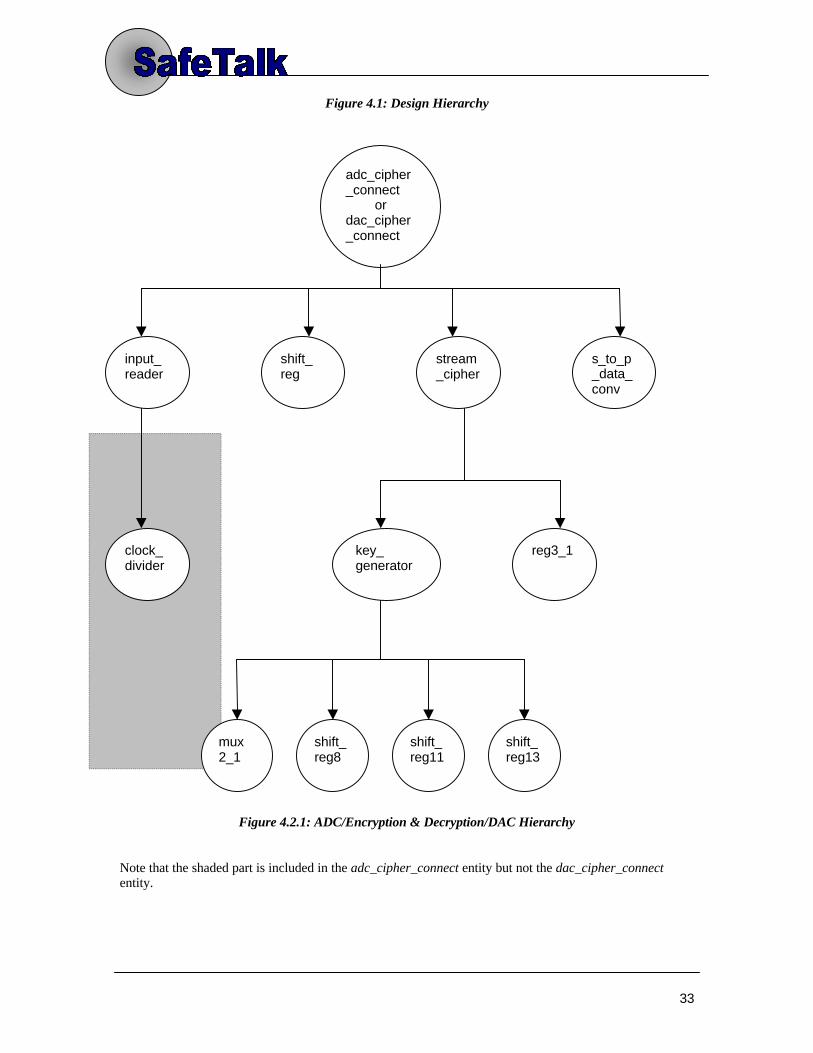
4. Design Hierarchy
The overview of the VHDL entities of SafeTalk is shown in Figure 3.1. Basically, the SafeTalkdesign consists of a controller that controls all the entities of the sub-sections. The controller isessential to the design since some of the entities run on different clock frequencies and hence, weneed the controller to provide synchronism.
The Encryption/Decryption module is broken up into two stages. See figure 3.3.11. ADC & Encryption
- adc_cipher_connect.vhd (interfaces the ADC hardware with theencryption algorithm)
- input_reader.vhd- stream_cipher.vhd
2. Decryption & DAC (interfaces the DAC hardware with the decryption algorithm) - dac_cipher_connect.vhd
- stream_cipher.vhd
The UART Transmit module is broken up into one stage.1. txmit – responsible for transmitting data and ensure proper framing and data parity
The UART Receive module is broken up into one stage.1. rxcver – accepts correct data from UART transmitter. See Section 2.3 for details.
Note : All VHDL codes stated above compiles without errors or bugs.
dsp_ctrl.vhd
SAFE TALK
txmit.vhd rxcver.vhd
adc_cipher_connect.vhd
input_reader.vhd
dac_cipher_connect.vhd
stream_cipher.vhd
ADC &Encryption Decryption &
DAC
UARTReceiveUART
Transmit
stream_cipher.vhd
33
Figure 4.1: Design Hierarchy
Figure 4.2.1: ADC/Encryption & Decryption/DAC Hierarchy
Note that the shaded part is included in the adc_cipher_connect entity but not the dac_cipher_connectentity.
adc_cipher_connect
ordac_cipher_connect
input_reader
s_to_p_data_conv
clock_divider
shift_reg
stream_cipher
mux2_1
reg3_1
shift_reg13
key_generator
shift_reg11
shift_reg8

34
5. FPGA Resources
5.1 ADC
The logic cells required for each component in the ADC is given below:
Table 5.2.1: Logic Cells for Encryption/Decryption
Component Number of Logic Cells Usedclock_divider (ADC) 6input_reader (ADC) 30
5.2 Encryption/Decryption
The logic cells required for each component in the stream cipher is given below:
Table 5.2.1: Logic Cells for Encryption/Decryption
Component Number of Logic Cells UsedShift_reg 39
S_to_p_data_conv 38Stream_cipher 38
Combining these components (and in the case of encryption, the ADC components) thehigher level entities require the number of logic cells listed below:
Table 5.2.2: Logic Cells for Encryption/Decryption
Entity Number of Logic Cells Usedadc_cipher_connect 138dac_cipther_connect 113
Total 251/1152 (22%)
5.3 Transmitter/Receive
The logic cells required for each component in the transmitter/receive is given below:
Table 5.3.1 Logic Cells for Tx/Rx
Entity Number of Logic Cells UsedUART 78
FIFO (2) 486Total 564/1152 (49%)
Total logic cells used: 886/1152 (76%)(dsp_ctrl.vhd – including all components)
35
6. Experimentation
6.1 Transmitter/Receive
Experiments were performed to test the different transmission rates that are attainable.Three different rates were tested as listed below.
- Baud rate of 98.3kbps framing and parity errors occurred.- Baud rate of 87.4kbps framing and parity errors also occurred.
It was found that although simulations showed that this rate was attainable, real lifetesting on the FPGA proved differently
The UART receiver module would not receive properly on the FPGA board butsimulated properly in MAX+Plus II. With experimentation we were able to get theFPGAs to receive the transmitted data without any framing or parity errors. At first itwas suspected that the transmission speed was set too high. This was not the case aftertesting it at lower speeds of about 9600 bps. We know that the UART transmits the startbit then the data with the LSB first. What we discovered is that if the LSB is a zero thereceiver will not receive correctly. On the other hand, if the LSB is a one the data isreceived correctly. This finding allowed us to transmit and receive correctly by settingthe LSB as always one. This does not affect the sample since it is at the LSB position.The difference between a one or a zero in the LSB would not change the analog signal byvery much. This would not be the case for the MSB.
The FIFO buffers that we used are 16x8-bits. This took up 243 logic cells, which is quitea large number. We tried to reduce this by decreasing the size from 16 to 8 but that onlydecreased the overall usage of logic cells by about 30. As a result we decided to staywith a 16 level FIFO.
6.2 Compression/Decompression
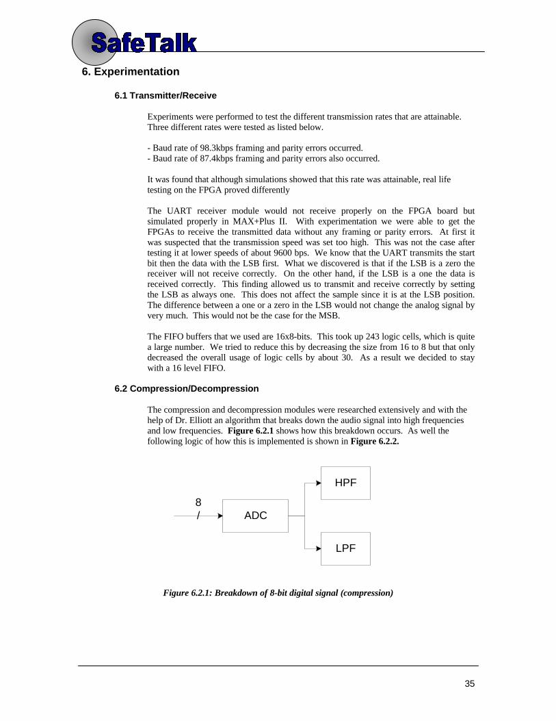
The compression and decompression modules were researched extensively and with thehelp of Dr. Elliott an algorithm that breaks down the audio signal into high frequenciesand low frequencies. Figure 6.2.1 shows how this breakdown occurs. As well thefollowing logic of how this is implemented is shown in Figure 6.2.2.
Figure 6.2.1: Breakdown of 8-bit digital signal (compression)
ADC
HPF
LPF
8/

36
Figure 2.5.2: Automatic Gain Adjuster
The design of the automatic gain adjuster was suggested to us by Dr. Elliott for use in thecompression of the digital speech signal. Figure 2.5.2 shows the gain adjuster with thelow frequency bits sampled at 1 in every 8 normally sampled bits, and 4 bits for everyhigh order bits.
8/
+
FF
Sample 1:8
>= 8/
//loadshiftReg.
1/
+
+
f( ) saturate
4/
5/

37
8. Research
8.1 Compression/Decompression
Compression and decompression of an audio signal is not used in SafeTalk for severalreasons that were researched and due to a lack of time was not implemented. Theconversion of an audio signal from analog to digital is simple however the data thatresults in the digital signal is large compared to the data needed to reconstruct it andconvert it back to analog. As a result a large speed modem—64Kbps—would berequired to send all the information. This modem speed could not be obtained thereforecompression is needed. Several algorithms were researched and are reported below forthe reasons why they were considered and why they were rejected.
The members did not have any basis as to how compression worked, and thereforeresearch started at the search engines on the Internet. The progression of compressionknowledge started with file data compression—lossless compression—and turned toadaptive differential pulse code modulation (ADPCM) with A-law and Mu-law—lossycompression. The group assumed that compression of an audio signal was researchedbefore, therefore, research continued for longer periods than reasonable for this project.
Arithmetic coding is a function of the probability of a digital sample and it’sencoding interval range. This compression takes a value and gives it a rangethat is between 0 and 1. The way arithmetic encoding works is that each 8-bitdigital value is given a probablility—for example 00000000 has a 10%probablilty of showing up. Next this probablility would be given an interval—inthe range from 0 to 1. The problem with this is that using digital logic we couldnot get the interval to break up into 256 segments nicely. Althoughconsideration was given to developing a different range value, the assumptionwas that other algorithms were already developed and this would require morework that was needed.
Run-length Coding was looked at as being a viable compression technique. Itworks best with redundant data that is repeated, and initially voice seemed to besomething that was repeated enough that this could be used. The reason for thisassumption was because the sample rate was very high—8KHz—so in terms ofthe sample rate being much, much higher than an average speech sample theredundancies could be reduced using this algorithm.
It turns out that this lossless algorithm could not be used because of the nature ofaudio sample. As well, the 8-bit sample does not have many redundant bits—asimages might have; therefore the run-length encoding was disregarded.
A form of compression—called dictionary method—uses combinations of dataand represents this as a smaller section of data. On the Internet variousalgorithms were found, and in particular the Lempel-Ziv algorithms wereconsidered. This is a lossless algorithm that seemed the best case, and stepswere taken to deepen the understanding of LZ algorithms. A version of LZ iscalled LZA seemed the most likely because the decompression time wasvirtually zero, so with the delay that we had in transmission, this was the firstcompression technique that started. C code was available for this and the initialcompilations took place.It was then pointed out that this was a lossless compression technique andlossless was not needed for audio compression.

38
Baffled at this point, a small investigation of how people in general perceivespeech. What was found was that at high frequencies—above 2KHz—thehuman ear uses envelope detection. This was good to know, considering thesampling rate could reconstruct signals that were up to 3.5KHz. Digital datathat was changing faster than 2KHz might not need to be accurate to reconstructthe exact signal.
In continuing with research, Dr. Elliott introduced a method that utilizeddynamic amplifier control. The way the algorithm works is that the audio signalis seperated into high amplitude and low amplitude. The most significant bits(MSB) of the 8-bit audio signal dominate the high amplitudes. Likewise theleast significant bits dominate the lower amplitudes. These two modes can besignified with a switch so that when people are going to shout then the higher 4bits could be used. The resulting bits over a modem would be 4bits/sample *8000 sample/sec = 32Kbps, which could work over a phone line.

39
9. References
[1] DAC data sheet : http://www.national.com/pf/DA/DAC0808.html[2] Microelectriconic Circuits by Sedra/Smith[3] Bruce Schneier, "Applied Cryptography", 2nd edition, John Wiley & Sons, Inc., 1996[4] Modern Digital and Analog Systems by B.P.Lathi[5] QuickLogic's Application Notes and QuickNoteshttp://www.quicklogic.com/support/anqn/(Digital UART Design Using Hardware Description Language)http://www.quicklogic.com/support/anqn/an20.pdf[6] MAX+Plus II v9.23MegaWizard Plug-In Manager[7] EE 552 Student Application Notes

40
10. Test Case Index
This section of the report basically describes all the test cases and simulations performedon all the sub-sections.
10.1 ADC
Test case 10.1.1:
Simulation of input_reader.vhd under normal conditions.Set EOC =’1’- End of conversion hence continue proceeding to next state offinite state machine. Set nreset =’1’- No reset wanted for this test case.Focusobservation on next_state that runs from one state to the other continuouslyon the simulation waveform.
Test Case 10.1.2:
Simulation waveform when the EOC signal is set to zero in the middle of theconversion i.e. conversion is not done yet. Focus observation on next_stateof simulation waveform. State remains at state 2 as long as the EOC signal iszero. State resumes to state 3 when EOC is set to one.
Test Case 10.1.3:Simulation waveform the signal EOC is set to zero for the entire duration. Focusobservation once more at next_state. State remains at state 2.
Test Case 10.1.4:
Simulation waveform when reset is set to zero. Note that reset is active low.Focus observation on next_state that returns to the initial state,sample_conv when the nreset signal is low.
Test Case 10.1.5:
For testing purposes of clock_divider.vhd, we will set the divisor valueto 1. This will decrease the normal clock period rate by a factor of 2 times.
Test Case 10.1.6:
The ADC and DAC are connected together. A function generator is used toproduce an input to the system. Output waveform is identical with the inputwaveform.
Test Case 10.1.7:
The ADC and DAC are connected together. An analog voice signal is used asam input through a microphone, and the output is observed on the oscilloscopeand heard through the speakers. Output waveform is similar to the inputwaveform except for some amplification and noise interference.

41
10.2 Encryption/Decryption
Test Case 10.2.1:
All three LFSRs are tested in the same manner. Each LFSR is seeded with ahard-coded key, the enable line is always high, and a clock with a 20.0ns periodis used. After every clock cycle, the LFSR outputs one bit. The value of thisbit, as well as the value stored in the register, is compared with the resultsobtained by hand.
Test Case 10.2.2:
During simulation of the keystream generator, the enable line is always high andthe clock has a period of 20.0ns. After every clock cycle, the keystreamgenerator outputs one bit. The value of this bit is compared with the resultsobtained by hand.
Test Case 10.2.3:
The stream cipher is simulated. Plaintext bits feed serially into one input of theregister, and the keystream feeds serially into the other register input. Theregister latches 1 bit from each input at the rising edge of every clock cycle.Then the two bits are XORed to produce a ciphertext bit. The output iscompared with the results obtained by hand.
Test Case 10.2.4:
The complete stream cipher (with the serial-to-parallel converter) is simulated.Inputs are fed serially, the encrypted output is sent 8 bits in parallel.
10.3 Transmitter/Receive
Test Case 10.3.1:
Transmit module testing (txmit.vhd)The testing of the transmitter was done by sending the transmitter therequired signals and data. Once the parallel input data of thetransmitter module is sent out of the serial line, the two values can becompared for validation. During the testing of the transmit module thebaud rate clock was set to divide the master clock by 4.
Test Case 10.3.2:
Receive module testing (rxcver.vhd)The testing of the receiver module was similar to the testing of thetransmitter module.
Test Case 10.3.3:
DSP module testing (dsp_ctrl.vhd)The testing of the DSP control transmitter was done by giving itparallel input of 6 different values. The serial output obtained werethen compared to the parallel input values to ensure propertransmission has taken place.

42
Test Case 10.3.4:
The testing of the DSP receiver control was similar but with the input as serialand the output as parallel. The inputs were compared to the outputs todetermine the validity of the reception.
Test Case 10.3.5:Testing of the entire project began with the simulations. The sub-componentsincluding the ADC controller, the encryption/decryption, andtransmission/reception are all connected appropriately. Testing of the projectwas similar to testing the dsp controller without the encryption/decryption. Withthe added encryption/decryption modules, which are clocked at a different speedthan the other modules, careful attention has to be considered concerning timingissues. With the testing through simulations, it was verified that the projectworks as it should.
10.4 DAC
Test Case 10.4.1:
A simple VHDL program that provides an 8-bit digital input to the DAC byusing switching is used. Each switch represented different input bit. Therefore,when all the switches were on, the digital input of the DAC would be 11111111.The result voltage Vout from the LF351 would be equal to Vout= 10V(1/2 +1/4+1/8 +1/16 +1/32 +1/64 +1/128 +1/256)= 9.96V according the formula thatgiven from the datasheet of the chips.
Test Case 10.4.2:
An 8-bit counter is used to produce digital inputs for the DAC. The counter isconstructed by VHDL code. The program produces 8-bit binary numbers toinput to the DAC. The counter counts up from 0 to 255 and then counts downfrom 255 back to 0. Again the results are compared with the values determinedby the Vout formula.
Test Case 10.4.3:
The ADC and DAC are connected together. A function generator is used toproduce an input to the system. Output waveform is identical with the inputwaveform.
Test Case 10.4.4:
The ADC and DAC are connected together. An analog voice signal is used asam input through a microphone, and the output is observed on the oscilloscopeand heard through the speakers. Output waveform is similar to the inputwaveform except for some amplification and noise interference.

43
11. Design Verification
To provide a concise explanation of the sequential steps performed to the various sub-sections, theflowchart below depicts clearly the overall process:
Testing Steps of Overall Project
ADC and DAC Test(refer to ADC and DAC Testing
Steps)
Encrption and DecryptionTest(refer to Encrption and Decryption
Testing Steps)
Transmission Test(refer to Transmission Design
Testing Steps)
SafeTalk Works

44
11.1 ADC
The flowchart below describes the sequential testing cases for the ADC and DAC:
StartADC Design
StartDAC Design
Does input_reader.vhd
compile andsimulateproperly?
Is theanalog-to-digital
converter hardwareworking as expected?
Combine bothDAC and ADC
circuits for testing
Does clock_divider.vhd
compile andsimulateproperly?
Doesdac.vhd
compile andsimulateproperly?
Is thedigital-to-analog
converter hardwareworking asexpected?
Yes Yes
Yes
Yes
Yes
Debugging tips:
(i) Probe input/outputp i n s a n d o b s e r v ew a v e f o r m w i t hoscillosccope to confirmcorrectness.( i i ) Run tes t casesthrough each chip toensure that the chipsa r e f u n c t i o n i n g a sdesired.(iii) Check all values ofcomponents (resistors,c a p a c i t o r s , e t c ) t oensure accuracy o fcomponents.( i i i ) I f a l l fa i ls , rewirecircuit.
NoDebug code,re-compile,re-simulate
and re-program ontoFLEX board.
No
Debugcode, re-compile,
re-simulateand re-program
onto FLEXboard.
NoDebug code,re-compile,re-simulate
and re-program ontoFLEX board.
Yes
Using thefunction generator as
the input signal, is theoutput signal from the DAC
similar to the input?
Using themicrophone (voice)
as the input signal, is theoutput signal from the DAC
similar to the input?
Yes
ADC & DAC hardwaresuccessfully achieve aim.
Yes
Are outputs asexpected?
Combine ADC withencryption code
for testing
Are outputs asexpected?
Combine DAC withdecryption code
for testing
Yes Yes
Encryption algorithm worksas expected when
connected with the ADC.
Decryption algorithm worksas expected when
connected with the DAC.
Checkconnectionson hardwareand confirmsimulation of
theencryption
code.
Checkconnectionson hardwareand confirmsimulation of
theencryption
code.
No
No
No
Refer tothe
debuggingtips above
Refer tothe
debuggingtips above
No
ADC and DAC Testing Steps-------------------------------------------------------------------------------------------------------------------------------------------------
No

45
11.1.1 Testing the Hardware
Connect the hardware to the function generator as the input waveform. Assign the pin assignmentson the FLEX20K board as follows:
Signal Pin Number Hole Number Signal Pin Number Hole NumberBit(0) 55 23 Data_out(0) 72 35Bit(1) 56 24 Data_out(1) 73 36Bit(2) 61 25 Data_out(2) 74 37Bit(3) 62 26 Data_out(3) 74 38Bit(4) 63 27 Data_out(4) 76 39Bit(5) 64 28 Data_out(5) 78 40Bit(6) 65 29 Data_out(6) 79 41Bit(7) 66 30 Data_out(7) 80 42Nreset - 28 Sample 83 45NEOC 81 43 Slow_clock 101 56SOC 82 44 Gnd Gnd 60
Then, the frequency desired is adjusted. The desired amplitude can also be fixed. Probe the EOC,SOC, sample and the clock signal with the oscilloscope probe. Observe waveform on theoscilloscope.Finally, the divisor value on the VHDL code clock_divider.vhd is changed. Increasing the divisorwould mean that the blinking of the LEDS would be faster. Decreasing it makes the LED blinksreally quickly.
ResultsOutput waveform is similar to the input waveform generated by the function oscillator for allcases. Circuit testing a success.
11.1.2 Testing the VHDL code clock_divider.vhd:
Using the divisor value of 2, the slow_clock will be 2 times slower than the regular clock.
Results:Slow_clock waveform is indeed slower than the period of clock by 2 times.
11.1.3 Testing the VHDL code input_reader.vhd:
Test case 1:
Waveform 1: Simulation under normal conditions.Set EOC=’1’- End of conversion hence continue proceeding to next state of finite statemachine. Set nreset=’1’- No reset wanted for this test case. Focus observation onnext_state that runs from one state to the other continuously on the simulationwaveform (as expected).
Test Case 2:
Waveform 2: Simulation waveform when the EOC signal is set to zero in the middle of theconversion i.e. conversion is not done yet. Focus observation on next_state ofsimulation waveform. State remains at state 2 as long as the EOC signal is zero. Stateresumes to state 3 when EOC is set to one.
46
Test Case 3:
Waveform 3: Simulation waveform the signal EOC is set to zero for the entire duration. Focus observation once more at next_state. State remains at state 2.
Test Case 4:
Waveform 4: Simulation waveform when reset is set to zero. Note that reset is active low.Focus observation on next_state that returns to the initial state, sample_convwhen the reset signal is low.
Results:All results of the 4 waveforms are as expected. Code input_reader.vhd is correct.
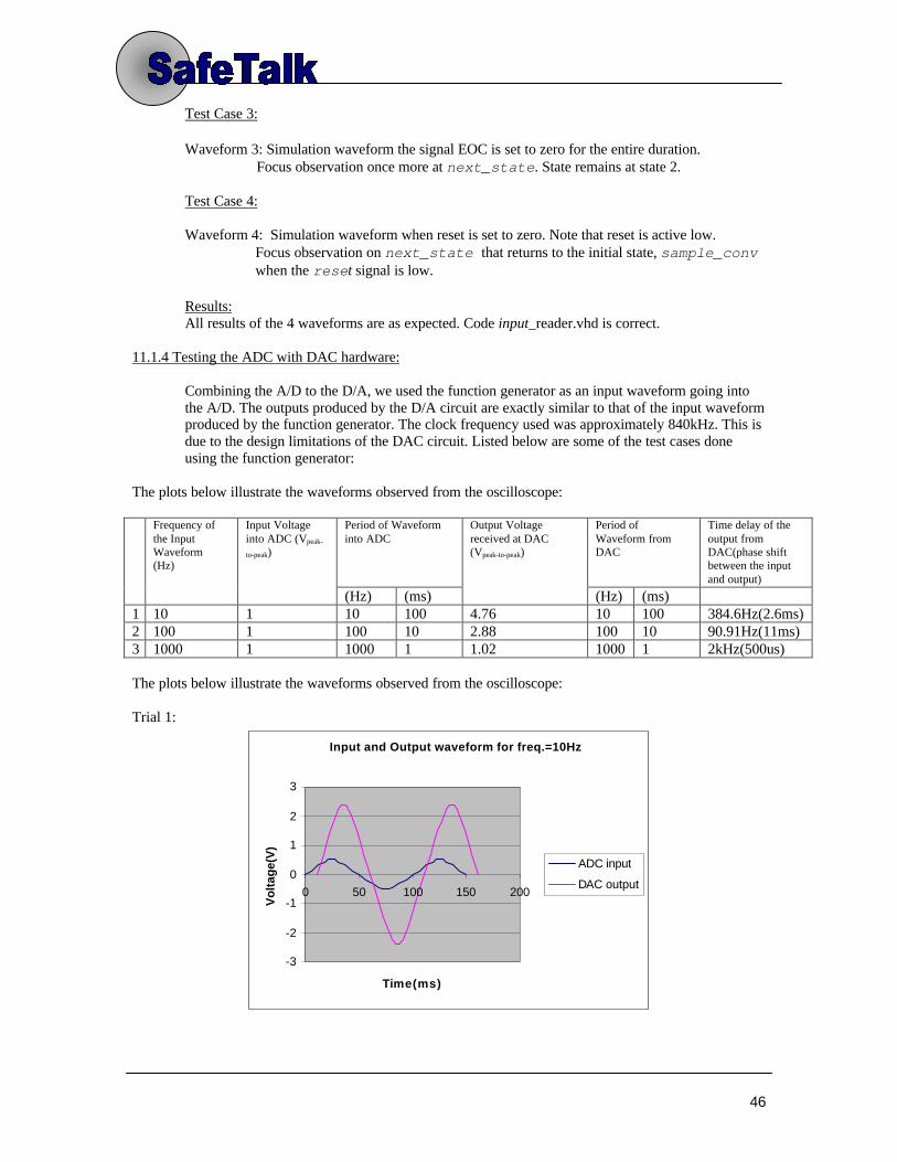
11.1.4 Testing the ADC with DAC hardware:
Combining the A/D to the D/A, we used the function generator as an input waveform going intothe A/D. The outputs produced by the D/A circuit are exactly similar to that of the input waveformproduced by the function generator. The clock frequency used was approximately 840kHz. This isdue to the design limitations of the DAC circuit. Listed below are some of the test cases doneusing the function generator:
The plots below illustrate the waveforms observed from the oscilloscope:
Period of Waveforminto ADC
Period ofWaveform fromDAC
Time delay of theoutput fromDAC(phase shiftbetween the inputand output)
Frequency ofthe InputWaveform(Hz)
Input Voltageinto ADC (Vpeak-
to-peak)
(Hz) (ms)
Output Voltagereceived at DAC(Vpeak-to-peak)
(Hz) (ms)1 10 1 10 100 4.76 10 100 384.6Hz(2.6ms)2 100 1 100 10 2.88 100 10 90.91Hz(11ms)3 1000 1 1000 1 1.02 1000 1 2kHz(500us)
The plots below illustrate the waveforms observed from the oscilloscope:
Trial 1:
Input and Output waveform for freq.=10Hz
-3
-2
-1
0
1
2
3
0 50 100 150 200
Time(ms)
Vo
ltag
e(V
)
ADC input
DAC output

47
Trial 2:
Input and Output waveform for freq.=100Hz
-2
-1.5
-1
-0.5
0
0.5
1
1.5
2
0 5 10 15 20
Time(ms)
Vo
ltag
e(V
)
ADC input
DAC output
Trial 3:
Input and Output waveform for freq.=1000Hz
-0.6
-0.4
-0.2
0
0.2
0.4
0.6
0 1 2 3
Time(ms)
Vo
ltag
e(V
)
ADC input
DAC output
Note : These graphs are plotted using MicroSoft Excel and the waveforms (lines) produced are very muchmore fine than the ones observed on the oscilloscope. Due to noise interference and other disturbances thatoccurred with the input signal, the sinusoidal waveform seen on the oscilloscope is courser and ‘dirtier’than the ones plotted using Excel.
The amplitudes of the input signal for the test cases 1 are fixed equal to 1Vpeak-to-peak.The inputand output waves are tested by probing the signals with the oscilloscope probe. The amplitude ofthe output voltage is greater than the input wave due to the fact of the amplifier. The waveformshows that the frequency of the output waveform is the same as the input wave. However, there isa phase shift between the input and output signal , it was found that the phase shift is due to thetime delay of the output and the delay became larger as the input signal frequency increased. Testcases was performed up to 1000Hz due to limitations of the ADC circuit. All of the input signals

48
with frequency greater than 3KHz will cutoff since the low-pass filter in the DAC was designed tohave a cut-off frequency of 3000Hz which is the bandwidth used in telephone communications.
11.2 Encryption/Decryption
The flowchart below describes the sequential testing cases for the encryption/decryptionalgorithm:
Start
Compiled and simulated VHDL code forencryption/decryption program without bugs
Testencryption/decryption program
with swithches and LEDs on theUP1 board. Are the outputs
as expected?
Testencryption with ADC
hardware. Are results asexpected?
Testdecryption with DAC
hardware. Are resultls asexpected?
Debug code andcheck thehardware
Debug code andcheck thehardware
Testthe encryption with
ADC and transmission, areoutputs asexpected?
Testthe encryption/decryption with
both ADC and DAC, aresimulations as
expected?
Testthe decryption with
DAC and receiver, are outputsresults asexpected?
Encryption andDecryption Works
Yes
NoNo
Yes Yes
Yes
NoDebug code. Re-compile and re-
simulate waveformto ensure
correctness.
Debug code. Re-compile and re-
simulate waveformto ensure
correctness.
Encryption andDecryption Testing
Steps----------------------------------
No
Debug code andcheck thehardware
Yes
No
Yes
Encryption works withADC and transmission.
Decryption works withDAC and receiver.

49
All three LFSRs are tested in the same manner. Each LFSR is seeded with a hard-codedkey, the enable line is always high, and a clock with a 20.0ns period is used. After everyclock cycle, the LFSR outputs one bit. The value of this bit, as well as the value stored inthe register, is compared with the results obtained by hand. These comparisons aresummarized in the tables below.
Table 11.2.1: LFSR-8 Test ResultsCorrect LFSRValue (Binary)
LFSR Value fromSimulation (Bin)
LFSR Value onWaveform (Hex)
Correct LFSROutput (Binary)
LFSR Outputfrom Simulation
(Bin)00001000 00001000 0810000100 10000100 84 0 001000010 01000010 42 0 010100001 10100001 A1 0 011010000 11010000 D0 1 111101000 11101000 E8 0 001110100 01110100 74 0 010111010 10111010 BA 0 011011101 11011101 DD 0 011101110 11101110 EE 1 101110111 01110111 77 0 000111011 00111011 3B 1 100011101 00011101 1D 1 100001110 00001110 0E 1 110000111 10000111 87 0 011000011 11000011 C3 1 101100001 01100001 61 1 100110000 00110000 30 1 100011000 00011000 18 0 0
Note: XORing bits 8, 4, 3, and 2 in the LFSR obtain the output bit.

50
Table 11.2.2: LFSR-11 Test ResultsCorrect LFSRValue (Binary)
LFSR Value fromSimulation (Bin)
LFSR Value onWaveform (Hex)
Correct LFSROutput (Binary)
LFSR Outputfrom Simulation
(Bin)00000001011 00000001011 00B10000000101 10000000101 405 1 111000000010 11000000010 602 1 101100000001 01100000001 301 0 000110000000 00110000000 180 1 100011000000 00011000000 0C0 0 000001100000 00001100000 060 0 000000110000 00000110000 030 0 000000011000 00000011000 018 0 000000001100 00000001100 00C 0 000000000110 00000000110 006 0 010000000011 10000000011 403 0 001000000001 01000000001 201 1 100100000000 00100000000 100 1 100010000000 00010000000 080 0 000001000000 00001000000 040 0 000000100000 00000100000 020 0 000000010000 00000010000 010 0 000000001000 00000001000 008 0 0
Note: XORing bits 11 and 2 in the LFSR obtain the output bit.
Table 11.2.3: LFSR-13 Test ResultsCorrect LFSRValue (Binary)
LFSR Value fromSimulation (Bin)
LFSR Value onWaveform (Hex)
Correct LFSROutput (Binary)
LFSR Outputfrom Simulation
(Bin)0000000001101 0000000001101 000D1000000000110 1000000000110 1006 1 10100000000011 0100000000011 0803 0 01010000000001 1010000000001 1401 1 10101000000000 0101000000000 0A00 1 10010100000000 0010100000000 0500 0 00001010000000 0001010000000 0280 0 00000101000000 0000101000000 0140 0 00000010100000 0000010100000 00A0 0 00000001010000 0000001010000 0050 0 00000000101000 0000000101000 0028 0 01000000010100 1000000010100 1014 0 00100000001010 0100000001010 080A 0 01010000000101 1010000000101 1405 0 01101000000010 1101000000010 1A02 1 11110100000001 1110100000001 1D01 0 00111010000000 0111010000000 0E80 1 10011101000000 0011101000000 0740 0 00001110100000 0001110100000 03A0 0 0
Note: XORing bits 13, 4, 3, and 1 in the LFSR obtains the output bit.
51
The keystream generator entity contains four components:1. an 8-bit maximal length linear feedback shift register2. a 11-bit maximal length linear feedback shift register3. a 13-bit maximal length linear feedback shift register4. a 2-to-1 multiplexer
The 8-bit LFSR output and the 11-bit LFSR output are used as the inputs to themultiplexer. The output of the 13-bit LFSR feeds into the multiplexer select line. Duringsimulation of this entity, the enable line is always high and the clock has a period of20.0ns. After every clock cycle, the keystream generator outputs one bit. The value ofthis bit is compared with the results obtained by hand as shown in the table below.
Table 11.2.4: Keystream Generator Test ResultsCorrect Generator Output Bit (Binary) Generator Output Bit from Simulation (Binary)
0 01 10 01 10 00 00 00 00 00 00 01 11 10 00 01 10 00 0
The stream cipher entity contains two components:1. a 1-bit 2-input register2. the key generator

52
Plaintext bits feed serially into one input of the register, and the keystream feeds seriallyinto the other register input. The register latches 1 bit from each input at the rising edgeof every clock cycle. Then the two bits are XORed to produce a ciphertext bit.
This entity compiles and simulates correctly. The test cases used are the following:1. plaintext stream of all 0's2. plaintext stream of all 1's3. plaintext stream pattern of 101010...
The results of these tests are summarized in the tables below.
Table 11.2.5: Plaintext Stream of All 0's Test CasePlaintext Bit
(Binary)Keystream Bit (Binary) Correct Ciphertext
(Binary)Ciphertext from
Simulation (Binary)0 0 0 00 1 1 10 0 0 00 1 1 10 0 0 00 0 0 00 0 0 00 0 0 00 0 0 00 0 0 00 0 0 00 1 1 10 1 1 10 0 0 00 0 0 00 1 1 10 0 0 00 0 0 0

53
Table 11.2.6: Plaintext Stream of All 1's Test CasePlaintext Bit
(Binary)Keystream Bit (Binary) Correct Ciphertext
(Binary)Ciphertext from
Simulation (Binary)1 0 1 11 1 0 01 0 1 11 1 0 01 0 1 11 0 1 11 0 1 11 0 1 11 0 1 11 0 1 11 0 1 11 1 0 01 1 0 01 0 1 11 0 1 11 1 0 01 0 1 11 0 1 1
Table 11.2.7: Plaintext Stream Pattern of 1010... Test CasePlaintext Bit
(Binary)Keystream Bit (Binary) Correct Ciphertext
(Binary)Ciphertext from
Simulation (Binary)1 0 1 10 1 1 11 0 1 10 1 1 11 0 1 10 0 0 01 0 1 10 0 0 01 0 1 10 0 0 01 0 1 10 1 1 11 1 0 00 0 0 01 0 1 10 1 1 11 0 1 10 0 0 0
The complete stream cipher contains a serial-to-parallel converter. The input data is fedserially. The output is the encrypted data, but it is sent 8 bits in parallel. The valid_inline is held high for 8 clock cycles indicating the inputs during that time are valid data.The output is not considered valid (and therefore, not read) until the valid_out line ishigh.

54
Table 11.2.8: Plaintext Stream of All 0's Test CasePlaintext Bit
(Binary)Correct Ciphertext in Serial
(Binary)Valid_out Ciphertext from Simulation
(Binary)0 0 0 000000000 1 0 000000000 0 0 000000000 1 0 000000000 0 0 000000000 0 0 000000000 0 0 000000000 0 0 000000000 1 000010100 0 0 000000000 0 0 000000000 0 0 000000000 1 0 000000000 1 0 000000000 0 0 000000000 0 0 000000000 1 0 000000000 1 10011000
Table 11.2.9: Plaintext Stream of All 1's Test CasePlaintext Bit
(Binary)Correct Ciphertext in Serial
(Binary)Valid_out Ciphertext from Simulation
(Binary)1 1 0 000000001 0 0 000000001 1 0 000000001 0 0 000000001 1 0 000000001 1 0 000000001 1 0 000000001 1 0 000000001 1 111101011 1 0 000000001 1 0 000000001 1 0 000000001 0 0 000000001 0 0 000000001 1 0 000000001 1 0 000000001 0 0 000000001 1 01100111
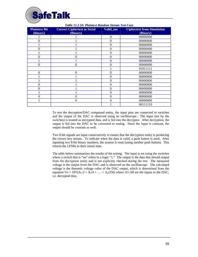
55
Table 11.2.10: Plaintext Random Stream Test CasePlaintext Bit
(Binary)Correct Ciphertext in Serial
(Binary)Valid_out Ciphertext from Simulation
(Binary)1 1 0 000000000 1 0 000000001 1 0 000000000 1 0 000000001 1 0 000000000 0 0 000000001 1 0 000000000 0 0 00000000
1 010111110 0 0 000000001 1 0 000000001 1 0 000000000 1 0 000000000 1 0 000000001 1 0 000000000 0 0 000000001 0 0 00000000
1 00111110
To test the decryption/DAC compound entity, the input pins are connected to switchesand the output of the DAC is observed using an oscilloscope. The input (set by theswitches) is treated as encrypted data, and is fed into the decryptor. After decryption, theoutput is fed into the DAC to be converted to analog. Since the input is constant, theoutput should be constant as well.
Two 8-bit signals are input consecutively to ensure that the decryption entity is producingthe correct key stream. To indicate when the data is valid, a push button is used. Afterinputting two 8-bit binary numbers, the system is reset (using another push button). Thisreturns the LFSRs to their initial state.
The table below summarizes the results of the testing. The input is set using the switcheswhere a switch that is “on” refers to a logic “1.” The output is the data that should outputfrom the decryption entity and is not explicitly checked during the test. The measuredvoltage is the output from the DAC and is observed on the oscilloscope. The calculatedvoltage is the theoretic voltage value of the DAC output, which is determined from theequation Vo = 10V(A1/2 + A2/4 + . . . + A8/256) where A1-A8 are the inputs to the DAC,i.e. decrypted data.

56
Table 11.2.11: Decryption/DAC Integration Test Results
Input – EncryptedData (Binary)
Output -- DecryptedData (Binary)
Measured Voltage(V)
Calculated Voltage(V)
11110101 11111111 10.20 9.9610101011 00110011 2.00 1.99
10100000 10101010 6.80 6.6400000011 10011011 6.20 6.05
00001010 00000000 0.00 0.0011011000 01000000 2.84 2.50
To test the ADC/Encryption compound entity, a function generator is connected to theinput pins and the output pins are connected to the DAC. The input waveform before theADC and the output waveform after the DAC are observed and compared using theoscilloscope. The outputs of the encryption entity are also observed on the oscilloscope.
Each output waveform from the 8 parallel bits of the encryption entity is a non-periodicsquare-waveform. This represents the logic 0s and 1s of the encrypted data. However,the rate at which this data is output is much too fast to check or display on LEDs. Theminimum speed at which the ADC can properly operate is still too fast for the human eyeto see. Thus, the outputs of the encryptor are fed into the DAC.
The output of the DAC is then compared to the input waveform. The output is anirregular, non-periodic waveform. It does not resemble the input waveform, as expected.The output of the encryptor should be noise, as confirmed.
11.3 Transmission/Receive
The flowchart below describes the sequential testing cases for the transmission/receive algorithm:

57
StartTransmission
Design
Test transmitter - txmit.vhd . Does code compile?
Are simulations asexpected?
Test receiver - rxcver.vhd . Does code
compile?Are simulations asexpected?
Testtransmitter& receiver
with controlller- dsp_control.vhd .Does code compile?Are
simulations asexpected?
Testtransmitter, receiver, &
controller with FIFO buffer - fifo.vhd. Does code compile?Are
simulations asexpected?
Testreceiver, transmitter,
controller, & fifo buffer withencryption/decrypytion codes. Does
code compile?Are simulationsas expected?
Test receiver, transmitter, controller,
fifo buffer, encyption/decryption codeswith hardware ADC and DAC. Are output
signals identical toinput signals?
SafeTalkworks!!
Yes
Yes
Yes
Yes
Yes
Yes
Debug code. Re-compile and re-simulate
waveforms to ensurecorrectness.
Debug code. Re-compile and re-simulate
waveforms to ensurecorrectness.
Debug code. Re-compile and re-simulate
waveforms to ensurecorrectness.
Debug code. Re-compile and re-simulate
waveforms to ensurecorrectness.
Debug code. Re-compile and re-simulate
waveforms to ensurecorrectness.
Debug code. Re-compile and re-simulate
waveforms to ensurecorrectness. Check
hardware.
No
No
No
No
No
No
Transmission Design Testing Steps-----------------------------------------------------------------------------------------------------------------------------------------------

58
Test Case 11.3.1
Transmit module testing (txmit.vhd)The testing of the transmitter was done by sending the transmitter the requiredsignals and data. Once the parallel input data of the transmitter module is sentout of the serial line, the two values can be compared for validation. During thetesting of the transmit module the baud rate clock was set to divide the masterclock by 4. This was done to reduce the size/length of the output waveform,thereby simplifying the verification of the waveform.
The 8-bit data bus was latched to four different values so that the outputs on theserial transmit line could be validated. The values used in the tests were EF, A5,55 and 00.
Table 11.3.1: Parallel Input vs. Serial Output
Expected serial outputParallel inputStart bit 8 data bits Parity bit (even) Stop bit
EF 0 11110111 1 1A5 0 10100101 0 155 0 10101010 0 100 0 00000000 0 1
Note: the 8 data bits are transmitted with LSB first.
Test Case 11.3.2
Receive module testing (rxcver.vhd)The testing of the receiver module was similar to the testing of the transmittermodule. The receiver module now functions correctly. It can be seen, from thewaveform, that the data was read in correctly from the serial input and correctlylatched to the receive hold register.
Table 11.3.2: Serial Input vs. Parallel Output
Expected serial inputStart bit 8 data bits Parity bit (even) Stop bit
Parallel output
0 11110111 1 1 EF0 10100101 0 1 A50 10101010 0 1 550 00000000 0 1 00
Note: the 8 data bits are received with LSB first.
The data chosen, for the testing of the transmitter and receiver modules, contain1’s and 0’s in varying orders thereby testing to ensure that the respectivemodules can interpret the received/transmitted serial signal.
Test Case 11.3.3
DSP module testing (dsp_ctrl.vhd)The testing of the DSP control transmitter was done by giving it parallel input of6 different values. The serial output obtained were then compared to the parallelinput values to ensure proper transmission has taken place.

59
Table 11.3.3: Parallel Input vs. Serial Output 2Expected serial outputParallel inputStart bit 8 data bits Parity bit (even) Stop bit
11 0 10001000 0 122 0 01000100 0 155 0 10101010 0 100 0 00000000 0 1A5 0 10100101 0 133 0 11001100 0 1Note: the 8 data bits are transmitted with LSB first.
The testing of the DSP receiver control was similar but with the input as serialand the output as parallel. The inputs were compared to the outputs todetermine the validity of the reception.
Table 11.3.4: Serial Input vs. Parallel Output 2Serial input
Start bit 8 data bits Parity bit (even) Stop bitExpectedParallel output
0 10001000 0 1 110 01000100 0 1 220 10101010 0 1 550 00000000 0 1 000 10100101 0 1 A50 11001100 0 1 33
Note: the 8 data bits are received with LSB first.
Note that the above DSP module tested contains the UART and FIFO buffers.
11.4 DAC
Test Case1:
In order to test the D/A converter, a simple VHDL code was used to assign thedigital inputs to the DAC0806 chip. Please refer to the VHDL code calleddac.vhd in the Appendix. The dac.vhd is a program that provides an 8-bit digitalinput to the DAC by switching the eight switch buttons. The code wasprogrammed on the EPF10K20 device of the UP1 Education Board. TheFLEX_SW1 switches were used to provide logic-level signals to eight-outputpin on the EPF10K20 device.

60
Table 11.4.1 : FLEX_EXPAN_A Signal Names & Device connections
Hole NumberOn the up1 board
Pin number for the DAC0806
15 12(LSB)16 1117 1018 919 820 721 622 5 (MSB)
The above hole number was connected to the input pins of the DAC0806 chipsaccording to the pin label of the chips. Each switch represented different inputbit. Therefore, when all the switches were on, the digital input of the DACwould be 11111111. The result voltage Vout from the LF351 would be equal toVout= 10V(1/2 +1/4 +1/8 +1/16 +1/32 +1/64 +1/128 +1/256)= 9.96V accordingthe formula that given from the datasheet of the chips.
Table 11.4.2: Test cases, test results and the calculated results.
The switches thatwere OFF
Digitalinput
TESTRESULT
(measuredvalues of
Vout)
Calculatedvalues ofVout(V)
None(all ON) 11111111 9.98 V 9.96S8 (Switch-8) 11111110 9.68 V 9.92S7 ,S8 11111100 9.52 V 9.84S6, S7, S8 11111000 9.44 V 9.68S5, S6, S7, S8 11110000 9.40 V 9.37S4, S5, S6, S7, S8 11100000 8.77 V 8.75S3, S4,S5, S6, S7, S8 11000000 7.52 V 7.50S2, S3, S4 S5, S6, S7, S8 10000000 5.91 V 5.00All 00000000 0.002 V 0.00
The measured voltage values from the test were very close to the calculatedvalues. This showed that the DAC part worked properly with the switch inputs.
Vout = Vref(A1/2 + A2/4+ A3/8+ A4/16 + A5/32 +A6/64 + A7/128 + A8/256),where Vref=10V , A1 to A8 represent the 8 digital inputs

61
Test Case 2:
The second test of the complete design of the Digital-to-Analog converter(DAC) is done by input the digital inputs by an 8-bits counter. The counter isconstructed by the VHDL code, and the program is called dsctest.vhd. Thisprogram provides an 8-bits counter, which produces 8-bits binary number inputto the DAC. The counter counts up from 0 to 255 and then counts down from255 back to 0. The output of the counter is an 8 bits binary number, which willgo to the 8-bits input of the DAC. The final output that produces from the DACis an analog signal. The result of the analog signal is a triangular waveform byinputting the counter digital input. The triangular waveform is shown on theoscilloscope in the demonstration and is plotted below:
Output waveform of the DAC
0
2
4
6
8
10
12
0 88 176 264 352
time(ms)
volt
age(
V)
Figure 11.4.1 : Output from DAC
The signal produced from the DAC shows that as the counter counts up fromzero to 255, the corresponding voltage increase from 0 to about 10V. The outputvoltage drops when the counter reaches 255 and then starts to count down. Aclock divider is used in the counter program to control the input time, the inputcomes into the DAC with frequency = 25.175MHz/ 10000 = 2517.2Hz. Thisfrequency can be change by changing the clock divider value.
After the connection of the low-pass filter, the output analog signal from thefilter becomes a smooth signal. The signal is sketched from the oscilloscope andis shown in the following diagram.
waveform after the Filter
02468
1012
0 100 200 300 400
time(ms)
volt
age(
V)
Figure 11.4.2: Filter Output

62
Test Case 3:
Combining the A/D to the D/A, we used the function generator as an input waveformgoing into the A/D. The outputs produced by the D/A circuit are exactly similar to that ofthe input waveform produced by the function generator. The clock frequency used wasapproximately 840kHz. This is due to the design limitations of the DAC circuit. Listedbelow are some of the test cases done using the function generator:
Input waveform was a sinusoidal wave.
Period of Waveforminto ADC
Period ofWaveform from
DAC
Time delay of theoutput fromDAC(phase shiftbetween the inputand output)
Frequency ofthe Input
Waveform(Hz)
Input Voltageinto ADC (Vpeak-
to-peak)
(Hz) (ms)
Output Voltagereceived at DAC
(Vpeak-to-peak)
(Hz) (ms)1 10 1 10 100 4.76 10 100 384.6Hz(2.6ms)2 100 1 100 10 2.88 100 10 90.91Hz(11ms)3 1000 1 1000 1 1.02 1000 1 2kHz(500us)
The plots below illustrate the waveforms observed from the oscilloscope:
Trial 1:
Input and Output waveform for freq.=10Hz
-3
-2
-1
0
1
2
3
0 50 100 150 200
Time(ms)
Vo
ltag
e(V
)
ADC input
DAC output
Figure 11.4.3
Trial 2:
Input and Output waveform for freq.=100Hz
-2
-1.5
-1
-0.5
0
0.5
1
1.5
2
0 5 10 15 20
Time(ms)
Vo
ltag
e(V
)
ADC input
DAC output

63
Figure 11.4.4Trial 3:
Input and Output waveform for freq.=1000Hz
-0.6
-0.4
-0.2
0
0.2
0.4
0.6
0 0.5 1 1.5 2 2.5
Time(ms)
Vo
ltag
e(V
)ADC input
DAC output
Figure 11.4.5
Note : These graphs are plotted using Microsoft Excel and the waveforms (lines)produced are very much more fine than the ones observed on the oscilloscope. Due tonoise interference and other disturbances that occurred with the input signal, thesinusoidal waveform seen on the oscilloscope is courser and ‘dirtier’ than the onesplotted using Excel.
The amplitudes of the input signal for the test cases 1 are fixed to be equal to1Vpeak-to-peak.The input and output waves are tested by probing the signalswith the oscilloscope probe. The amplitude of the output voltage is greater thanthe input wave due to the fact of the amplifier. The waveform shows that thefrequency of the output waveform is the same as the input wave. However, thereis a phase shift between the input and output signal, due to the propagationdelay. From observation of the results, the delay increases with the input signalfrequency. Test cases was performed up to 1000Hz due to limitations of theADC circuit. All of the input signals with frequency greater than 3KHz willcutoff since the low-pass filter in the DAC and ADC was designed to have a cut-off frequency of 3000Hz (bandwidth used in telephone communications).
12. VHDL Source Code Index♦ clock_divider.vhd♦ input_reader.vhd♦ comp.vhd♦ p_out_stream_cipher_pkg.vhd♦ p_out_stream_cipher.vhd♦ s_to_p_data_conv.vhd♦ txmit.vhd♦ rxcver.vhd♦ fifo.vhd♦ dsp_ctrl_pkg.vhd♦ dsp_ctrl.vhd♦ dsctest.vhd♦ dac.vhd

64
13. Test Bench Index
♦ clock_divider_test.vhd♦ comp_test.vhd♦ dsp_testbench.vhd♦ dac_test.vhd

65
A. Appendix : Data Sheets
SafeTalk
SafeTalk prototype v1.0Secure Telecommunications Module
General Description:SafeTalk is used for secure telecommunication where privacy is desired.
Features:- Secure telecommunication with a companion
(v1.0 has basic encryption. Later implementations will incorporate strongerencryption)- Asynchronous data transmission using a UART.
Key Specifications:- 8-bit linear ADC- 8-bit linear DAC- Stream cipher encryption/decryption- Asynchronous data transmission using a UART
Functional Description:SafeTalk uses an 8-bit linear ADC and DAC for conversion between analog and digital.The digital signal processing performed includes encryption and decryption of the digitalsamples. With version 1.0 no compression or decompression has been implemented. Asa result the data rate required for transmission is higher than it should be. At a samplingrate of 8000 kHz, the data rate required is about 88 kbps. The modem that we would usewith SafeTalk would have a data rate of 33.6 kbps. With compression this data ratewould be achievable.
Logic blocks required: 884


