35
Scanning Probe Microscopy Danny Porath 2002 (Eigler et. al.@IBM)
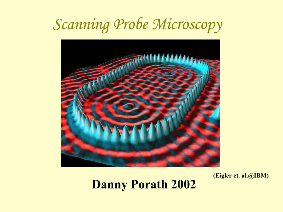
Scanning Probe Microscopy
Danny Porath 2002(Eigler et. al.@IBM)

Introduction to Scanning Probe Microscopy and applications.
Julio Gómez Herrero. LNM. UAM
“SPM - the eyes to the Nano world”.
With the help of…….
1. Yosi Shacam – TAU2. Yossi Rosenwacks – TAU3. Julio Gomez-Herrero - UAM4. Serge Lemay - Delft5. Hezy Cohen6. …

Outline SEM/TEM:1. Examples, links and homework
2. STM principle, lab, Images
3. Tunneling
4. Instrumentation
5. Artifacts
6. Spectroscopy
7. Lithography
Books and Internet Sites“Scanning Probe Microscopy and Spectroscopy”, R.
Wiesendanger (Cambridge U. Press)
http://www.embl-heidelberg.de/~altmann/
http://www.chembio.uoguelph.ca/educmat/chm729/STMpage/stmtutor.htmhttp://www.weizmann.ac.il/surflab/peter/afmworks/index.html
http://www.almaden.ibm.com/almaden/media/image_mirage.html...
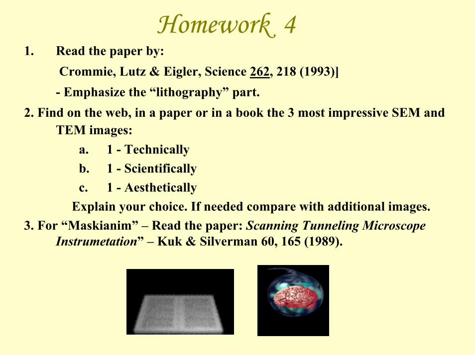
Homework 41. Read the paper by:
Crommie, Lutz & Eigler, Science 262, 218 (1993)] - Emphasize the “lithography” part.
2. Find on the web, in a paper or in a book the 3 most impressive SEM and TEM images:
a. 1 - Technicallyb. 1 - Scientificallyc. 1 - Aesthetically
Explain your choice. If needed compare with additional images.3. For “Maskianim” – Read the paper: Scanning Tunneling Microscope
Instrumetation” – Kuk & Silverman 60, 165 (1989).

Scanning Tunneling Microscope (STM)
Sample
Piezo
Electronics(Current+Feedback)
Computer(Control)
Matrix ofheights(Image)
Tip
I(V) ~ Ve-(ks)
Tunneling between a sharp tip and conducting surface.Piezo enables xy and z movement.Working modes: constant current and constant height.The feedback voltage Vz(x,y) is translated to height (topographic) information.
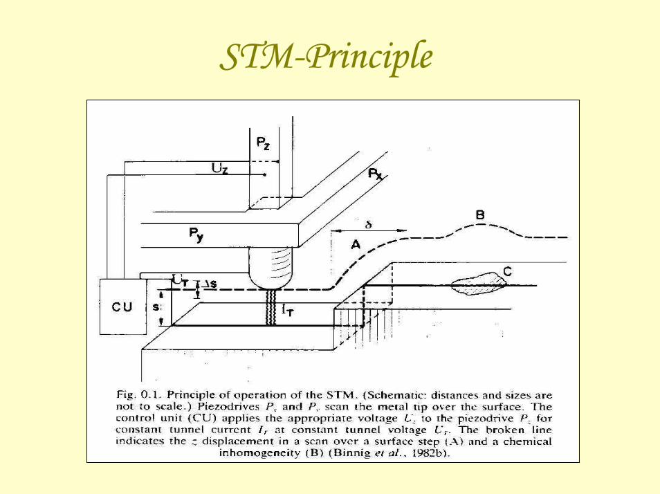
STM-Principle

STM Head
דגם
בידוד
בסיס
STM - ראש ה
חוד
בורגמיקרו-מטרי
גבישפייזו-אלקטרי
רכיבי היחידה המרכזית
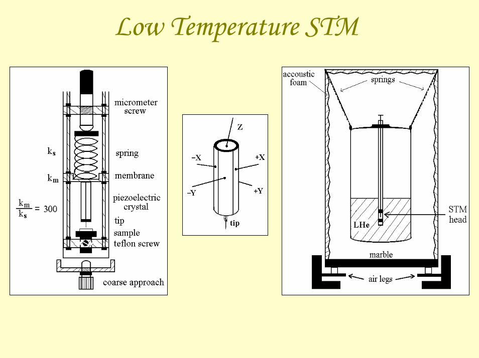
Low Temperature STM

Low Temperature STM
בורג מיקרומטרי
מוט קפיץ
ממברנהגביש
פייזואלקטרי
חוד
רכיבקרוב גס
מחזיקהדגם
מחזיקהדגם

STM Laboratory
STM
חיפויעץ
אלקטרוניקה
מערכתהמחשב
בסיס
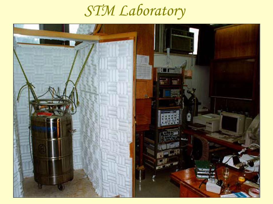
STM Laboratory
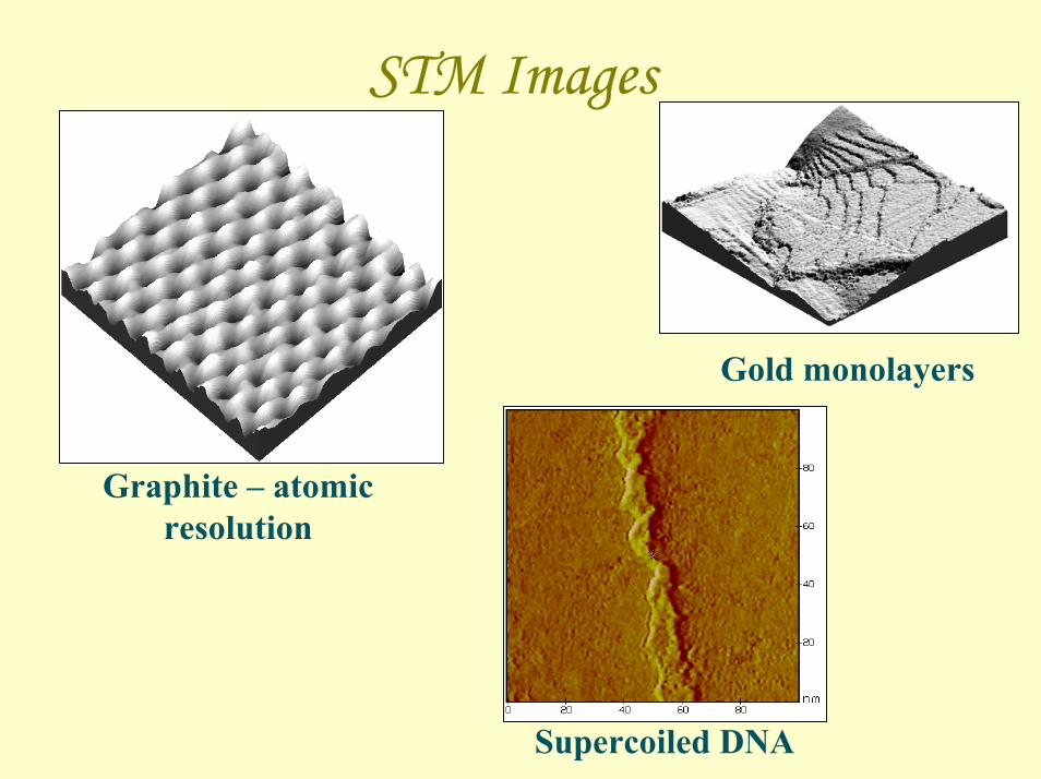
STM Images
Graphite – atomic resolution
Supercoiled DNA
Gold monolayers

STM image of a Single-Wall Carbon Nanotube

Si (111) Surface (7x7 reconstruction)

STM Images Combination GaSb/InAsOnly every-other lattice plane is exposed on the (110) surface,
where only the Sb (reddish) and As (blueish) atoms can
This color-enhanced 3-D rendered STM image shows the atomic-scale structure of the interfaces between GaSb and InAs in cross-section. A superlattice of alternating GaSb (12 monolayers) and InAs (14 monolayers) was grown by molecular beam epitaxy. A piece of the wafer was cleaved in vacuum to expose the (110) surface, and then the tip was positioned over the superlattice about 1 µm from the edge. Due to the structure of the crystal, only every-other lattice plane is exposed on the (110) surface, where only the Sb (reddish) and As (blueish) atoms can be seen. The atoms are 4.3 Å apart along the rows, with a corrugation of <0.5 Å From work of W. Barvosa-Carter, B. R. Bennett, and L. J. Whitman..

Inspection
Tip techniqueswith CCD-camera for on-chip inspectionStylus (α-step)
Height resolution 5 nmLateral resolution ≥ 15 µm
AFMHeight resolution monolayerLateral resolution ≤ nm
MicroscopyOptical microscopy (1 µm) Dark field, Interference contrast, luminescence Scanning Electron M. (≤ 1 nm)
20-25% of fabrication time!

Why STM ?The electronic microscopes gives ‘volume images’ (penetration depth)In STM-no use of external particlesPrinciple-Electrons tunneling between an atomically sharp tip and a surface
STM-Introduction

The STM combines three main concepts:
• Scanning• Tunneling• Tip-point probing
• Uniqueness:
STM-Introduction
Animation: http://www.iap.tuwien.ac.at/www/surface/stm_gallery/stm_animated.gif

STM-HistoryIn March 1981, Gerd Binning, H. Rohrer, Ch. Gerber and E. Weibel observed electrons tunneling in vacuum between W tip and Pt; this in combination with scanning marked the birth of STM.
The breakthrough: atomic-scale surface imaging in real space
The development of STM paved the way for a new family of techniques called : “scanning probe microscopy”.
1986-Nobel prize to G. Binnig and H. Rohrer.

The first STM image

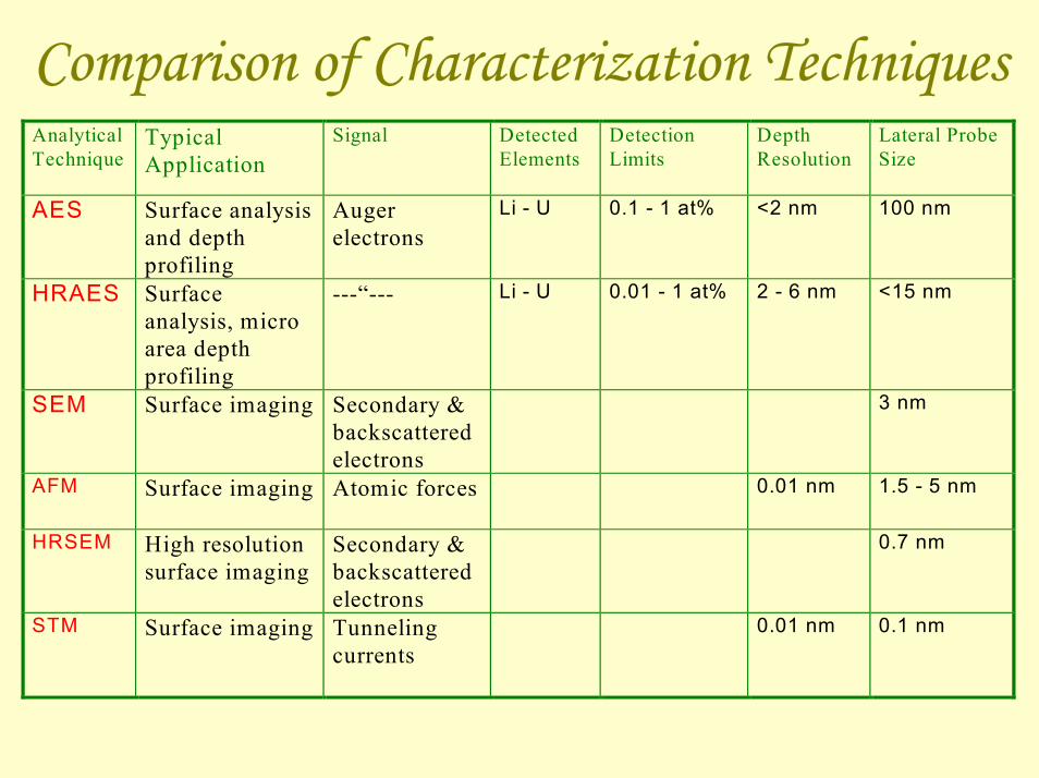
Comparison of Characterization TechniquesAnalyticalTechnique
TypicalApplication
Signal DetectedElements
DetectionLimits
DepthResolution
Lateral Probe Size
TXRF Metalcontamination
X-rays S - U 109-1012Atoms/cm2
10 mm
RBS Thin filmcomposition
He atoms Li - U 1 - 10 at%(Z<20)0.01 - 1(Z>20)
2-20 nm 2 mm
XPS Surface analysisDepth profiling
Photo-electrons
Li - U 0.01 - 1 at% 1-10 nm 10 µm – 2 mm
EDAX(EDS)
elementalmicroanalysis
X-rays B - U 0.1 - 1 at% 1 – 5 µm 1 µm
QuadSIMS
DopantprofilingSurfacemicroanalysis
Secon-dary ions
H - U 1014-1017Atoms/cm3
<5 nm 1 µm (Imaging)30 µm (D Profiling)
TOFSIMS
Surfacemicroanalysis
Secon-dary ions
H - U 108Atoms/cm2
<1monolayer
0.1 µm (Imaging)
Comparison of Characterization TechniquesAnalytical Technique
Typical Application
Signal Detected Elements
Detection Limits
Depth Resolution
Lateral Probe Size
AES Surface analysis and depth profiling
Auger electrons
Li - U 0.1 - 1 at% <2 nm 100 nm
HRAES Surface analysis, micro area depth profiling
---“--- Li - U 0.01 - 1 at% 2 - 6 nm <15 nm
SEM Surface imaging Secondary & backscattered electrons
3 nm
AFM Surface imaging
Atomic forces
0.01 nm 1.5 - 5 nm
HRSEM High resolution surface imaging
Secondary & backscattered electrons
0.7 nm
STM Surface imaging Tunneling currents
0.01 nm 0.1 nm
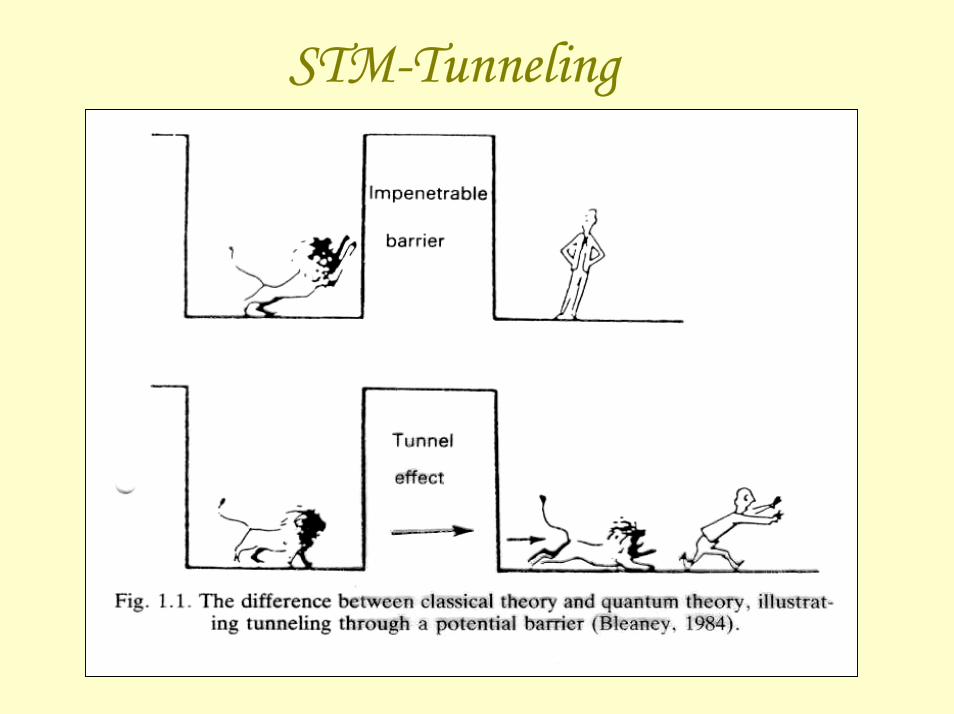
STM-Tunneling

STM-Tunneling

STM-Tunneling Models
Elastic vs. Inelastic (energy loss to phonons etc) tunneling processes
One dimensional vs. three dimensional
Barrier shape
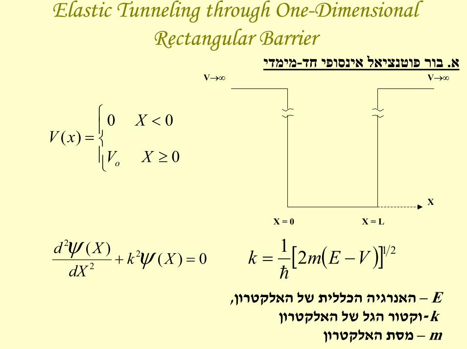
Elastic Tunneling through One-Dimensional Rectangular Barrier
X
V→∞ V→∞
X = LX = 0
≥
<=
0
00)(
XV
XxV
o
0)()( 2
2
2
=+ XkdXXd ψψ ( )[ ] 2121 VEmk −=
hE –ה אנרגיה הכל לי ת של האל קטרון ,
k-וקט ור הגל של ה אלקט רוןm –מ סת הא לקטרון
א. בור פוט נצ י אל אי נ סופ י ח ד-מימדי
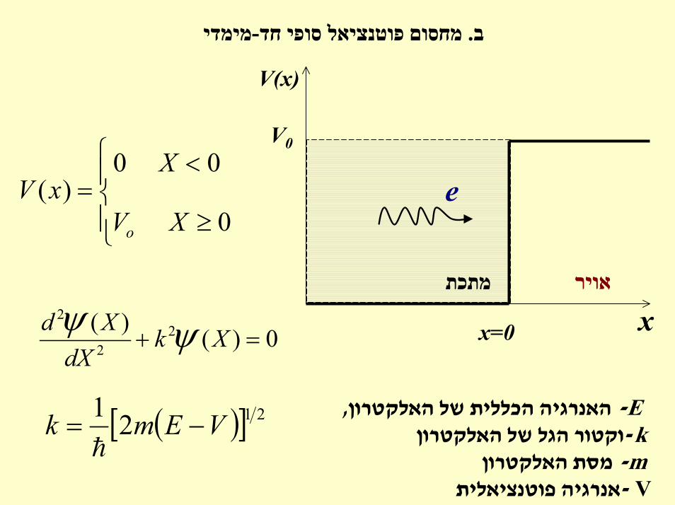
מימדי -פוט נצ יא ל סופ י ח ד מחסום. ב
≥
<=
0
00)(
XV
XxV
o
0)()( 2
2
2
=+ XkdXXd ψψ
( )[ ] 2121 VEmk −=h
E- האנרגיה הכללי ת של האל ק טרון , k-וקט ור הגל של ה אלקט רון m- מ סת הא לקטרון
V - אנרגיה פ וטנציאלי ת
V(x)
xמתכת אויר
e
V0
x=0

)המשך (ממדי-פוט נצ יאל סו פי חד מחסום
xikxik BeAexx 11)( ;0 −+=< ψ
xEVm
xEVm
xVEm
ixVEm
i
DeCe
DeCexx
hh
hh
)(2)(2
)(2)(2
00
00
)( ;0−
+−−
−−
−
+=
=+=≥ ψ
מתכת אויר
e
V0
X=0
[ ] )21( 211 mEk
h=
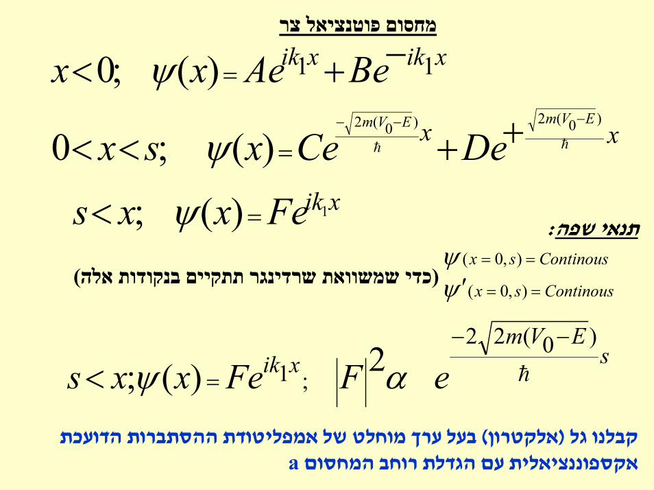
xikxik BeAexx 11)( ;0 −+< =ψxx
EVmEVm
DeCexsx hh
)0(2)0(2
)( ;0−−− ++<< =ψ
xikFexxs 1)( ; =< ψ
Continoussx
Continoussx
==
==
′ ),0(
),0(
ψψ
: ת נאי שפ ה
sEVm
xik eFFexxs h
)0(22
;1 2)(;−−
=< αψה ה סתברות הדועכת בעל ערך מוחלט של אמ פ ליטודת) אלקטרון (קבלנו גל
aעם הגדל ת רוחב ה מ חסום אקס פוננציאלי ת
מחסום פוט נצ יאל צר
)תתקי ים בנקודות אלהשרדי נגר כדי ש משוואת (

e
x
V(x)
V0
מתכתאויר מתכת
e
x=0 x=s
מי נהור-מחסום פוט נצ יאל צר
ses
EVmxik eFFexxs καψ 2
)0(22
;1 2)(; −=
−−
=< h
כל פעם שמ תרח ק ים eהס תב רות למצוא את הא לקטרון יורדת פי : מרח ק של
)(2221
0 EVm −−
=h
κ

Å 1בצד השנ י של מ חסום ברוחב של הס ת ברות למצוא אלקט רוןה e/1ה יא Vo-E =1.0 eVכאשר
מרח ק ז ה הוא בקירוב (1. ה הס תב רות הי א Å 2~רוחב מ חסום של עבור ) ה מרח ק הבין אטומי
e
x
V(x)
V0
מתכתאויר מתכתe
x=0 x=s
Ψ (x)
x
מי נהור
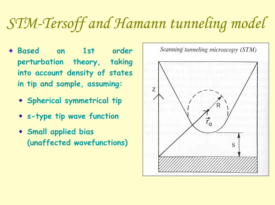
STM-Tersoff and Hamann tunneling modelBased on 1st order perturbation theory, taking into account density of states in tip and sample, assuming:
Spherical symmetrical tip
s-type tip wave function
Small applied bias (unaffected wavefunctions)
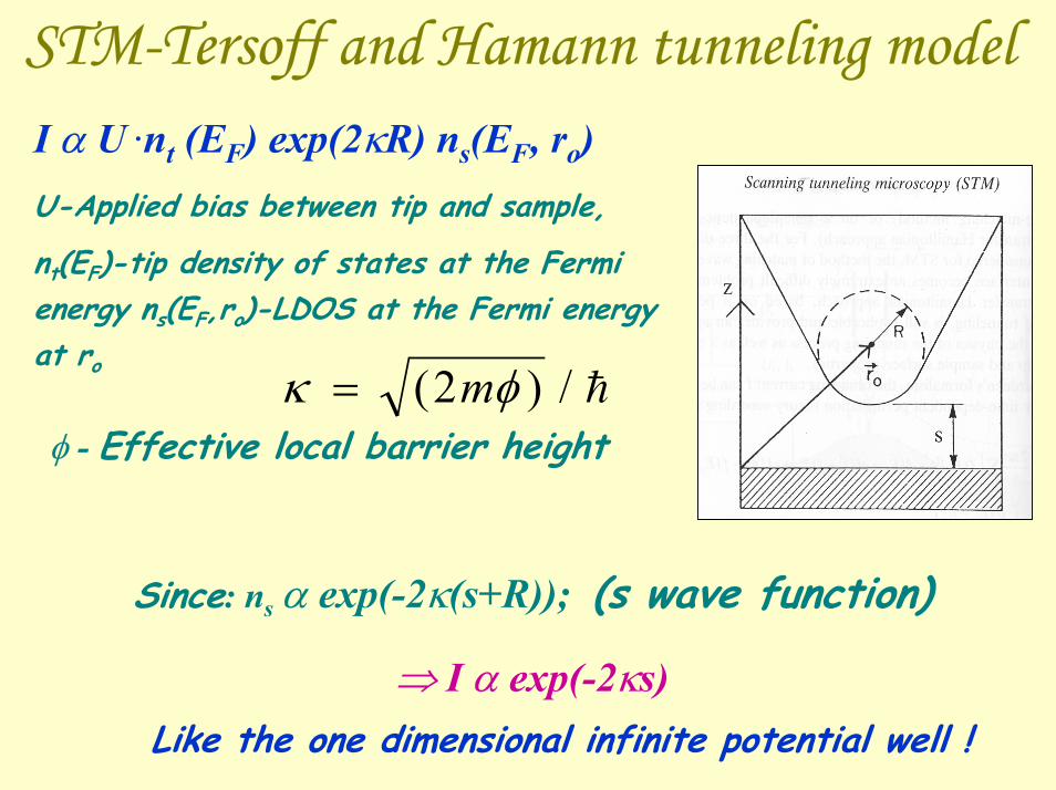
STM-Tersoff and Hamann tunneling model
φ - Effective local barrier height
Since: ns α exp(-2κ(s+R)); (s wave function)
⇒ I α exp(-2κs)
h/)2( φκ m=
I α U .nt (EF) exp(2κR) ns(EF, ro)U-Applied bias between tip and sample,
nt(EF)-tip density of states at the Fermienergy ns(EF,ro)-LDOS at the Fermi energy at ro
Like the one dimensional infinite potential well !


