SCANNING TRANSMISSION ELECTRON MICROSCOPY:AN EXPERIMENTAL TOOL FOR ATOMIC SCALE
INTERFACE SCIENCE
N. D. Browning1, E. M. James1, K. Kishida1, I. Arslan1, J. P. Buban1, J. A. Zaborac1,S. J. Pennycook2, Y. Xin1,2 and G. Duscher1,2*
1Department of Physics (M/C 273), University of Illinois at Chicago, 845 West Taylor Street, Chicago, IL 60607-7059. USA.2Solid State Division, Oak Ridge National Laboratory, P.O. Box 2008, Oak Ridge, TN 37831-6030. USA.
* Current address: Department of Physics and Astronomy, Vanderbilt University, Nashville, TN, USA
Received: October 30, 1999
Abstract. Although internal interfaces have long been known to dominate the performance of many materialssystems critical to modern technology, there has yet been little incontrovertible evidence pointing to thefundamental origin of the structure-property relationships. However, the recent development of direct imagingand analysis techniques in the scanning transmission electron microscope (STEM) has provided a newexperimental pathway to obtain information on the local atomic structure, chemical composition and bondingat interfaces on the fundamental atomic scale. This is precisely the information that is required to unravelthe complexities of interfaces and opens up a new paradigm for investigating the structure-propertyrelationships at internal interfaces. In this paper we discuss the practical aspects of the experimental STEMtechniques and demonstrate the resolution possible in current commercially available instrumentation. Theapplication of these techniques to the study of internal interfaces is highlighted by a discussion of theanalysis of homophase interfaces in SrTiO
3, Bi
2Sr
2Ca
2Cu
3O
10 and YBa
2Cu
3O
7-δ and the heterophase interfacesbetween GaAs and Au, and between Si and molecular beam epitaxy (MBE) grown II-VI semiconductors.
Corresponding author: Prof. Nigel D. Browning, e-mail: [email protected]
Internal interfaces have long been known to be the keyto many mechanical and electrical properties [1,2].Extensive microstructural evaluations have been per-formed recently on for example, metal-oxide interfaces[3-5], semiconductor-oxide interfaces [6,7], semicon-ductor-metal interfaces [8,9] and grain boundaries [10-14] important for a wide variety of technological ap-plications. In many cases, the length scale over whichthe analysis was performed depends on the particularproperty that was being tested for, and more often thannot, the availability of high-spatial resolutioninstrumentation. Obviously, the study of interfaces is ahuge field and we cannot hope to cover it all here. Inthis paper, therefore, we concentrate on the analysis ofinterfaces where understanding the complexities of thestructure-property relationships requires fundamentalatomic scale information. In particular, we will describethe requirements for the instrumentation to obtain theatomic scale information and will focus on the recentlydeveloped incoherent Z-contrast imaging [15] and elec-tron energy loss spectroscopy (EELS) [16] techniquesin the scanning transmission electron microscope
(STEM). Furthermore, we will describe the use of ba-sic theoretical models to correlate multiple imagingand analytical techniques together and finally, presentsome examples demonstrating materials interface prob-lems where these techniques have provided fundamen-tal atomic scale information on the structure-propertyrelationships.
2. EXPERIMENTAL TECHNIQUES
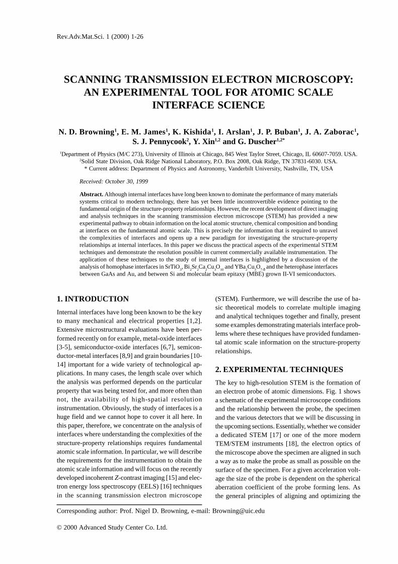
The key to high-resolution STEM is the formation ofan electron probe of atomic dimensions. Fig. 1 showsa schematic of the experimental microscope conditionsand the relationship between the probe, the specimenand the various detectors that we will be discussing inthe upcoming sections. Essentially, whether we considera dedicated STEM [17] or one of the more modernTEM/STEM instruments [18], the electron optics ofthe microscope above the specimen are aligned in sucha way as to make the probe as small as possible on thesurface of the specimen. For a given acceleration volt-age the size of the probe is dependent on the sphericalaberration coefficient of the probe forming lens. Asthe general principles of aligning and optimizing the
Rev.Adv.Mat.Sci. 1 (2000) 1-26
� ��������������������
probe are the same for all STEMs we only discuss herethe specifics of probe formation in the JEOL 2010FTEM/STEM as an example of how the process worksexperimentally [18, 19].
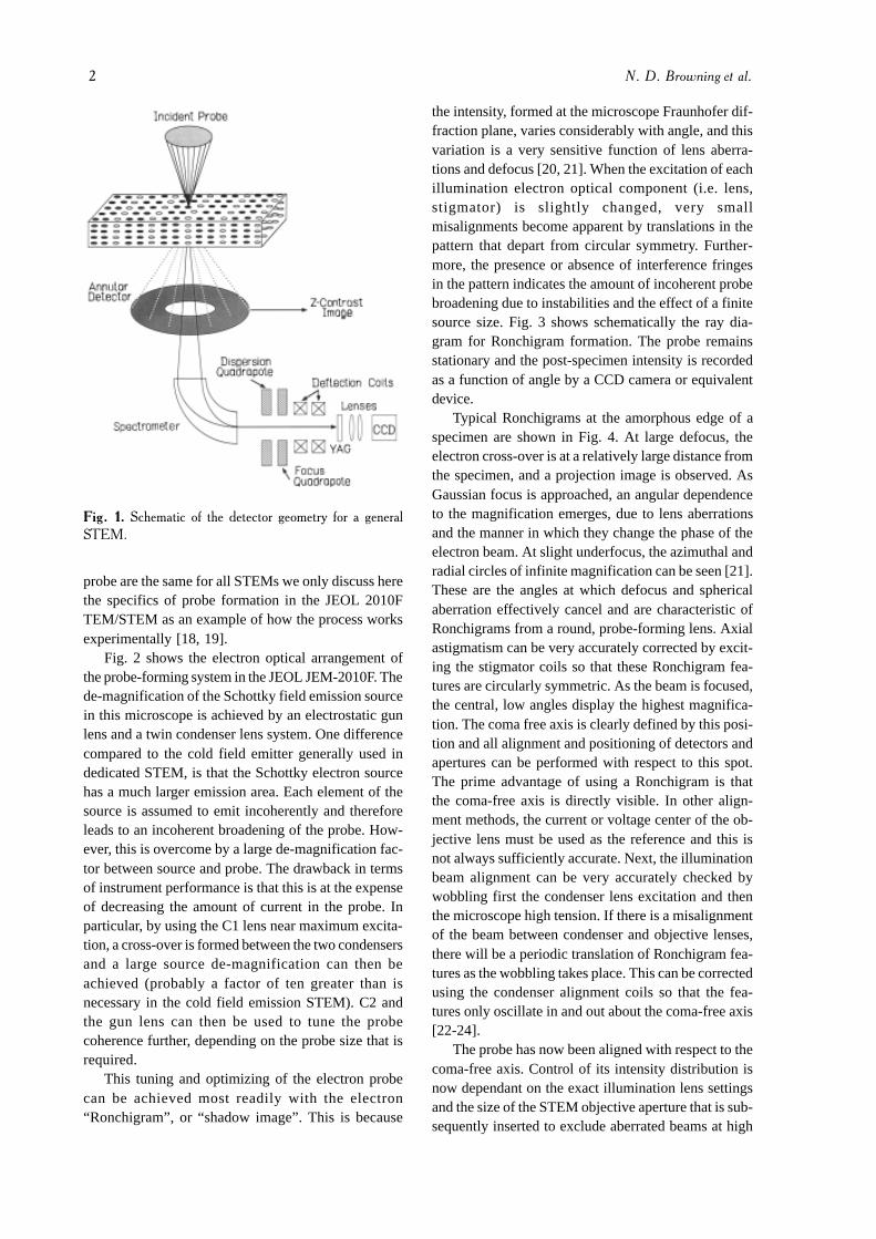
Fig. 2 shows the electron optical arrangement ofthe probe-forming system in the JEOL JEM-2010F. Thede-magnification of the Schottky field emission sourcein this microscope is achieved by an electrostatic gunlens and a twin condenser lens system. One differencecompared to the cold field emitter generally used indedicated STEM, is that the Schottky electron sourcehas a much larger emission area. Each element of thesource is assumed to emit incoherently and thereforeleads to an incoherent broadening of the probe. How-ever, this is overcome by a large de-magnification fac-tor between source and probe. The drawback in termsof instrument performance is that this is at the expenseof decreasing the amount of current in the probe. Inparticular, by using the C1 lens near maximum excita-tion, a cross-over is formed between the two condensersand a large source de-magnification can then beachieved (probably a factor of ten greater than isnecessary in the cold field emission STEM). C2 andthe gun lens can then be used to tune the probecoherence further, depending on the probe size that isrequired.
This tuning and optimizing of the electron probecan be achieved most readily with the electron“Ronchigram”, or “shadow image”. This is because
the intensity, formed at the microscope Fraunhofer dif-fraction plane, varies considerably with angle, and thisvariation is a very sensitive function of lens aberra-tions and defocus [20, 21]. When the excitation of eachillumination electron optical component (i.e. lens,stigmator) is slightly changed, very smallmisalignments become apparent by translations in thepattern that depart from circular symmetry. Further-more, the presence or absence of interference fringesin the pattern indicates the amount of incoherent probebroadening due to instabilities and the effect of a finitesource size. Fig. 3 shows schematically the ray dia-gram for Ronchigram formation. The probe remainsstationary and the post-specimen intensity is recordedas a function of angle by a CCD camera or equivalentdevice.
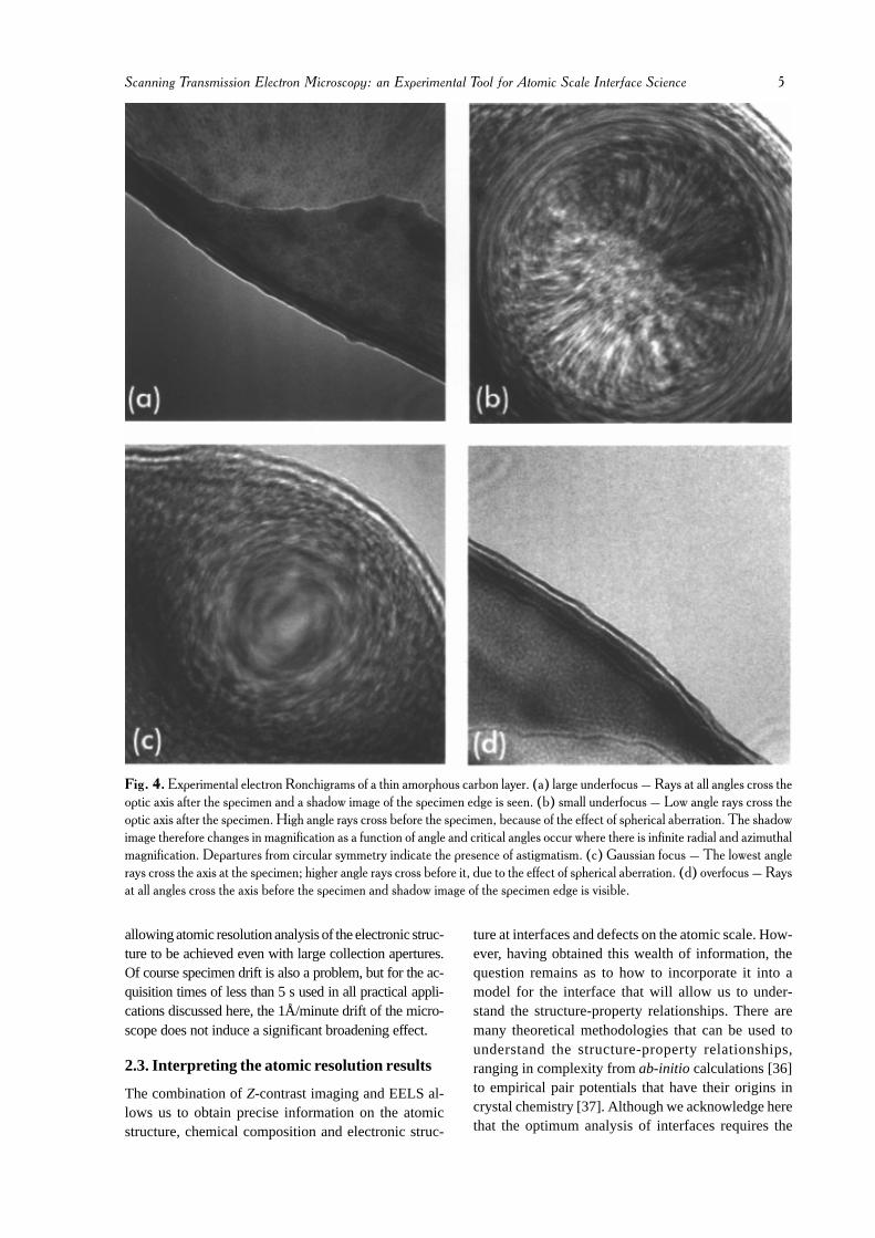
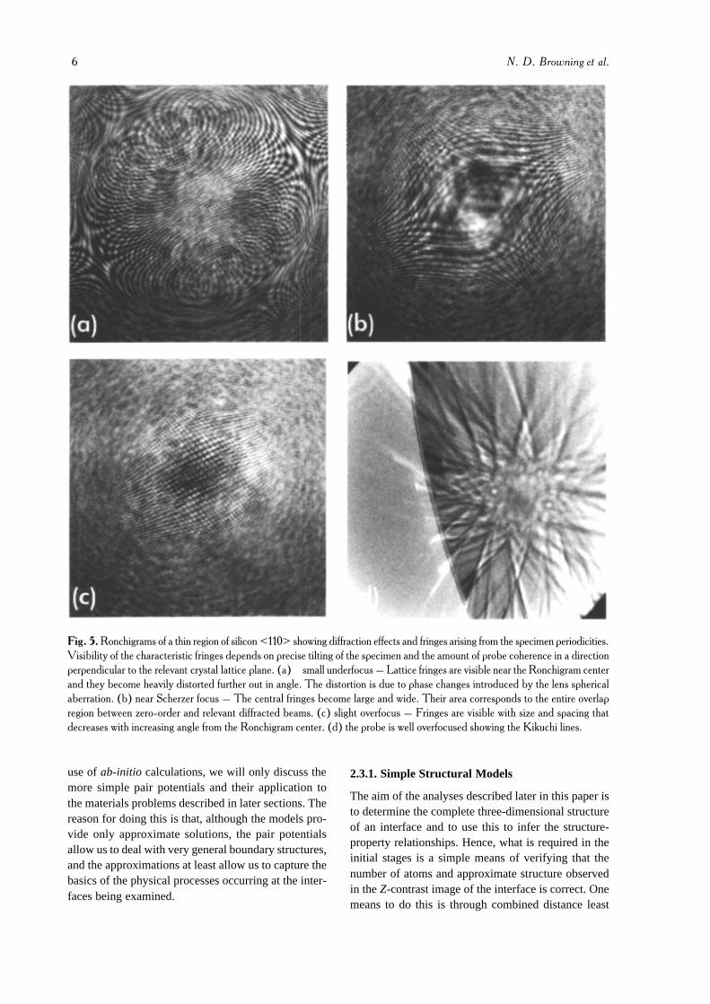
Typical Ronchigrams at the amorphous edge of aspecimen are shown in Fig. 4. At large defocus, theelectron cross-over is at a relatively large distance fromthe specimen, and a projection image is observed. AsGaussian focus is approached, an angular dependenceto the magnification emerges, due to lens aberrationsand the manner in which they change the phase of theelectron beam. At slight underfocus, the azimuthal andradial circles of infinite magnification can be seen [21].These are the angles at which defocus and sphericalaberration effectively cancel and are characteristic ofRonchigrams from a round, probe-forming lens. Axialastigmatism can be very accurately corrected by excit-ing the stigmator coils so that these Ronchigram fea-tures are circularly symmetric. As the beam is focused,the central, low angles display the highest magnifica-tion. The coma free axis is clearly defined by this posi-tion and all alignment and positioning of detectors andapertures can be performed with respect to this spot.The prime advantage of using a Ronchigram is thatthe coma-free axis is directly visible. In other align-ment methods, the current or voltage center of the ob-jective lens must be used as the reference and this isnot always sufficiently accurate. Next, the illuminationbeam alignment can be very accurately checked bywobbling first the condenser lens excitation and thenthe microscope high tension. If there is a misalignmentof the beam between condenser and objective lenses,there will be a periodic translation of Ronchigram fea-tures as the wobbling takes place. This can be correctedusing the condenser alignment coils so that the fea-tures only oscillate in and out about the coma-free axis[22-24].
The probe has now been aligned with respect to thecoma-free axis. Control of its intensity distribution isnow dependant on the exact illumination lens settingsand the size of the STEM objective aperture that is sub-sequently inserted to exclude aberrated beams at high
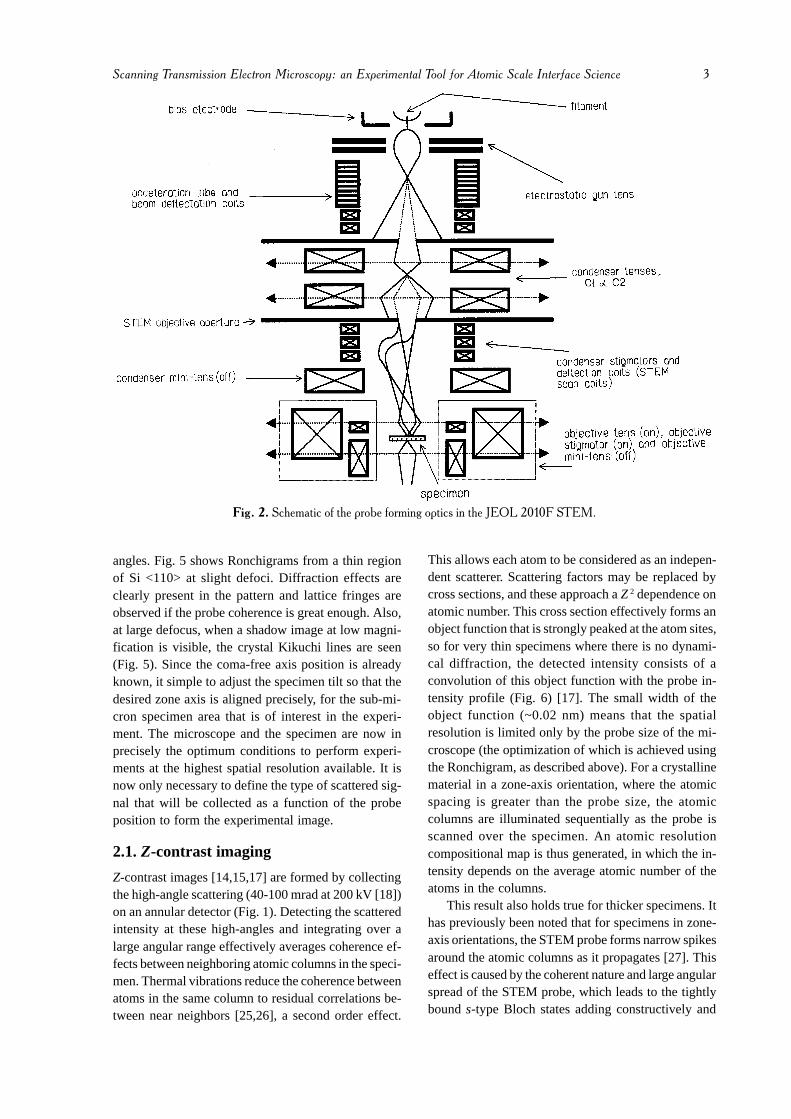
angles. Fig. 5 shows Ronchigrams from a thin regionof Si <110> at slight defoci. Diffraction effects areclearly present in the pattern and lattice fringes areobserved if the probe coherence is great enough. Also,at large defocus, when a shadow image at low magni-fication is visible, the crystal Kikuchi lines are seen(Fig. 5). Since the coma-free axis position is alreadyknown, it simple to adjust the specimen tilt so that thedesired zone axis is aligned precisely, for the sub-mi-cron specimen area that is of interest in the experi-ment. The microscope and the specimen are now inprecisely the optimum conditions to perform experi-ments at the highest spatial resolution available. It isnow only necessary to define the type of scattered sig-nal that will be collected as a function of the probeposition to form the experimental image.
2.1. Z-contrast imaging
Z-contrast images [14,15,17] are formed by collectingthe high-angle scattering (40-100 mrad at 200 kV [18])on an annular detector (Fig. 1). Detecting the scatteredintensity at these high-angles and integrating over alarge angular range effectively averages coherence ef-fects between neighboring atomic columns in the speci-men. Thermal vibrations reduce the coherence betweenatoms in the same column to residual correlations be-tween near neighbors [25,26], a second order effect.
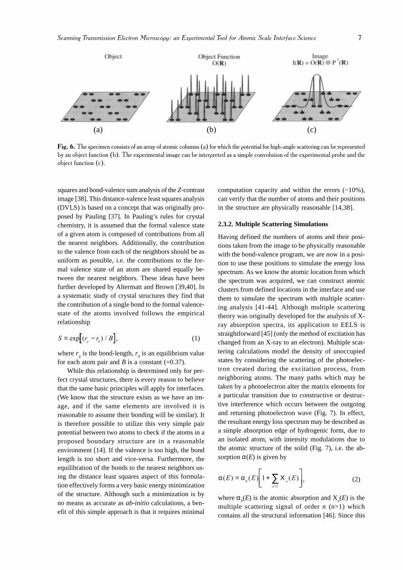
This allows each atom to be considered as an indepen-dent scatterer. Scattering factors may be replaced bycross sections, and these approach a Z 2 dependence onatomic number. This cross section effectively forms anobject function that is strongly peaked at the atom sites,so for very thin specimens where there is no dynami-cal diffraction, the detected intensity consists of aconvolution of this object function with the probe in-tensity profile (Fig. 6) [17]. The small width of theobject function (~0.02 nm) means that the spatialresolution is limited only by the probe size of the mi-croscope (the optimization of which is achieved usingthe Ronchigram, as described above). For a crystallinematerial in a zone-axis orientation, where the atomicspacing is greater than the probe size, the atomiccolumns are illuminated sequentially as the probe isscanned over the specimen. An atomic resolutioncompositional map is thus generated, in which the in-tensity depends on the average atomic number of theatoms in the columns.
This result also holds true for thicker specimens. Ithas previously been noted that for specimens in zone-axis orientations, the STEM probe forms narrow spikesaround the atomic columns as it propagates [27]. Thiseffect is caused by the coherent nature and large angularspread of the STEM probe, which leads to the tightlybound s-type Bloch states adding constructively and
! ��������������������
the less localized states interfering destructively [17].This effect is enhanced for scattering processes suchas high-angle thermal diffuse scattering that arelocalized at the atomic cores, causing a great reductionin beam broadening. With only one dominant Blochstate, dynamical diffraction effects are largely removedand manifest only as a columnar channeling effect, thusmaintaining the thin specimen description of the im-age as a simple convolution of the probe intensity pro-file and an object function, strongly peaked at the atomsites (Fig. 6).
The phase problem associated with the interpreta-tion of conventional high-resolution TEM images istherefore eliminated. In thin specimens, the dominantcontribution to the intensity of a column is always itscomposition, although due to the higher absorption ofthe heavy strings the contrast does decrease with in-creasing specimen thickness and in very thick crystalsthere is no longer a high resolution image. The effectof changing focus is also intuitively understandable asthe focus control alters the probe intensity profile onthe surface of the specimen. For defocus less than theoptimum Scherzer condition, the probe broadenscausing the individual columns not to be resolved. Forhigher defocus values the probe narrows with the for-mation of more intense tails, causing sharper imagefeatures but compositional averaging over severalcolumns. The optimum focus condition thereforerepresents a compromise between high resolution(narrow probe profile) and the desire for a highly localimage (no significant tails to the probe). This also
corresponds to the optimum probe for microanalysis[16, 28, 29].
At defects and interfaces, structures can becomeextremely complicated, causing difficulties in deter-mining the precise 3-dimensional composition. How-ever, provided an atomic column is continuous throughthe crystal, reconstructions will only result in a changein column intensity and not a contrast reversal [14].The atomic structure in the region of defects and inter-faces can therefore still be determined largely from theimage, and used to position the electron probe for EELS[16, 28, 29].
2.2. Electron energy loss spectroscopy (eels)
As can be seen from Fig. 1, the annular detector usedfor Z-contrast imaging does not interfere with the low-angle scattering used for EELS [30]. This means thatthe Z-contrast image can be used to position the elec-tron probe over a particular structural feature for ac-quisition of a spectrum [16, 28, 29]. The physical prin-ciple behind EELS relates to the interaction of the fastelectron with the sample to cause either collective ex-citations of electrons in the conduction band, or dis-crete transitions between atomic energy levels, e. g.1s→2p transitions [30]. The ability to observe discreteatomic transitions allows compositional analysis to beperformed by EELS (the transitions occur atcharacteristic energy losses for a given element). Fur-thermore, the transitions to unoccupied states abovethe Fermi level allows the degree of hybridization be-tween atomic orbitals to be determined, i.e. informationon local electronic structure (bonding) changes can beascertained.
To be able to correlate the spectrum precisely withthe structural feature seen in the image, it is essentialthat the spectrum have the same atomic resolution asthe Z-contrast image. In order to achieve this atomicresolution, the range over which a fast electron cancause an excitation event must be less than the inter-atomic spacing. Hydrogenic models [31,32] show thatfor the majority of edges accessible by conventionalenergy-loss spectrometers (∆E < 2 keV) the object func-tions are localized within 0.1 nm of the atom cores[33-35]. Hence, like the Z-contrast image, we have anobject function localized at the atom cores and an ex-perimental probe of atomic dimensions. For crystallinematerials in zone-axis orientations, providing wemaintain a large collection angle (15-30 mrad),coherent effects will be averaged and the descriptionof the spectrum in terms of a convolution of the probewith an object function is valid (Fig. 6). An importantaspect of this experimental approach is that the probechanneling discussed for Z-contrast imaging will alsopreserve the spatial resolution of the spectrum, thereby
allowing atomic resolution analysis of the electronic struc-ture to be achieved even with large collection apertures.Of course specimen drift is also a problem, but for the ac-quisition times of less than 5 s used in all practical appli-cations discussed here, the 1Å/minute drift of the micro-scope does not induce a significant broadening effect.
2.3. Interpreting the atomic resolution results
The combination of Z-contrast imaging and EELS al-lows us to obtain precise information on the atomicstructure, chemical composition and electronic struc-
ture at interfaces and defects on the atomic scale. How-ever, having obtained this wealth of information, thequestion remains as to how to incorporate it into amodel for the interface that will allow us to under-stand the structure-property relationships. There aremany theoretical methodologies that can be used tounderstand the structure-property relationships,ranging in complexity from ab-initio calculations [36]to empirical pair potentials that have their origins incrystal chemistry [37]. Although we acknowledge herethat the optimum analysis of interfaces requires the
use of ab-initio calculations, we will only discuss themore simple pair potentials and their application tothe materials problems described in later sections. Thereason for doing this is that, although the models pro-vide only approximate solutions, the pair potentialsallow us to deal with very general boundary structures,and the approximations at least allow us to capture thebasics of the physical processes occurring at the inter-faces being examined.
2.3.1. Simple Structural Models
The aim of the analyses described later in this paper isto determine the complete three-dimensional structureof an interface and to use this to infer the structure-property relationships. Hence, what is required in theinitial stages is a simple means of verifying that thenumber of atoms and approximate structure observedin the Z-contrast image of the interface is correct. Onemeans to do this is through combined distance least
squares and bond-valence sum analysis of the Z-contrastimage [38]. This distance-valence least squares analysis(DVLS) is based on a concept that was originally pro-posed by Pauling [37]. In Pauling’s rules for crystalchemistry, it is assumed that the formal valence stateof a given atom is composed of contributions from allthe nearest neighbors. Additionally, the contributionto the valence from each of the neighbors should be asuniform as possible, i.e. the contributions to the for-mal valence state of an atom are shared equally be-tween the nearest neighbors. These ideas have beenfurther developed by Altermatt and Brown [39,40]. Ina systematic study of crystal structures they find thatthe contribution of a single bond to the formal valence-state of the atoms involved follows the empiricalrelationship
� � � ���
= −��� � � ��
, (1)
where rij is the bond-length, r
0 is an equilibrium value
for each atom pair and B is a constant (=0.37).While this relationship is determined only for per-
fect crystal structures, there is every reason to believethat the same basic principles will apply for interfaces.(We know that the structure exists as we have an im-age, and if the same elements are involved it isreasonable to assume their bonding will be similar). Itis therefore possible to utilize this very simple pairpotential between two atoms to check if the atoms in aproposed boundary structure are in a reasonableenvironment [14]. If the valence is too high, the bondlength is too short and vice-versa. Furthermore, theequilibration of the bonds to the nearest neighbors us-ing the distance least squares aspect of this formula-tion effectively forms a very basic energy minimizationof the structure. Although such a minimization is byno means as accurate as ab-initio calculations, a ben-efit of this simple approach is that it requires minimal
computation capacity and within the errors (~10%),can verify that the number of atoms and their positionsin the structure are physically reasonable [14,38].
2.3.2. Multiple Scattering Simulations
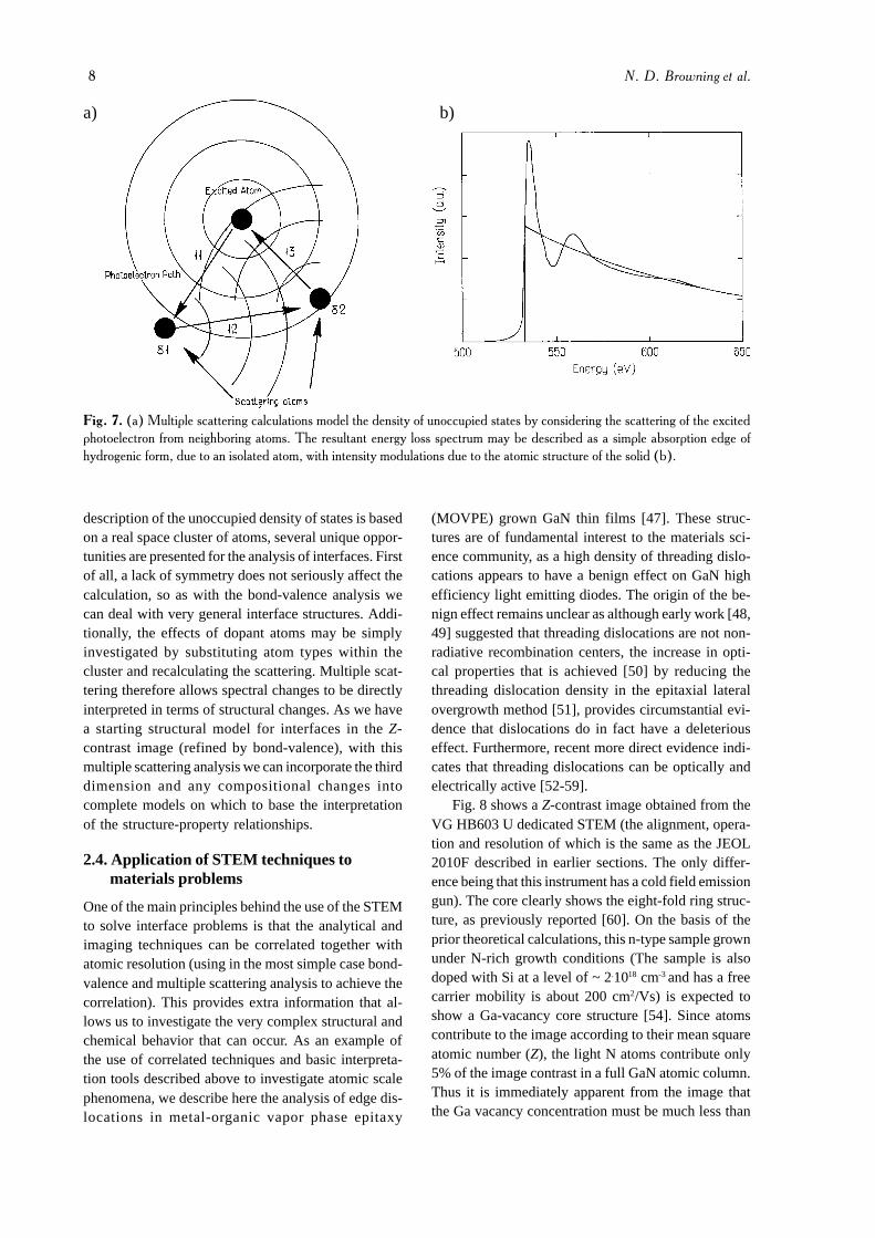
Having defined the numbers of atoms and their posi-tions taken from the image to be physically reasonablewith the bond-valence program, we are now in a posi-tion to use these positions to simulate the energy lossspectrum. As we know the atomic location from whichthe spectrum was acquired, we can construct atomicclusters from defined locations in the interface and usethem to simulate the spectrum with multiple scatter-ing analysis [41-44]. Although multiple scatteringtheory was originally developed for the analysis of X-ray absorption spectra, its application to EELS isstraightforward [45] (only the method of excitation haschanged from an X-ray to an electron). Multiple scat-tering calculations model the density of unoccupiedstates by considering the scattering of the photoelec-tron created during the excitation process, fromneighboring atoms. The many paths which may betaken by a photoelectron alter the matrix elements fora particular transition due to constructive or destruc-tive interference which occurs between the outgoingand returning photoelectron wave (Fig. 7). In effect,the resultant energy loss spectrum may be described asa simple absorption edge of hydrogenic form, due toan isolated atom, with intensity modulations due tothe atomic structure of the solid (Fig. 7), i.e. the ab-sorption α(E) is given by
α α� � � � � �� � ��
�
= +=
∑�
���
���
�
Χ , (2)
where α0(E) is the atomic absorption and X
n(E) is the
multiple scattering signal of order n (n>1) whichcontains all the structural information [46]. Since this
description of the unoccupied density of states is basedon a real space cluster of atoms, several unique oppor-tunities are presented for the analysis of interfaces. Firstof all, a lack of symmetry does not seriously affect thecalculation, so as with the bond-valence analysis wecan deal with very general interface structures. Addi-tionally, the effects of dopant atoms may be simplyinvestigated by substituting atom types within thecluster and recalculating the scattering. Multiple scat-tering therefore allows spectral changes to be directlyinterpreted in terms of structural changes. As we havea starting structural model for interfaces in the Z-contrast image (refined by bond-valence), with thismultiple scattering analysis we can incorporate the thirddimension and any compositional changes intocomplete models on which to base the interpretationof the structure-property relationships.
2.4. Application of STEM techniques to materials problems
One of the main principles behind the use of the STEMto solve interface problems is that the analytical andimaging techniques can be correlated together withatomic resolution (using in the most simple case bond-valence and multiple scattering analysis to achieve thecorrelation). This provides extra information that al-lows us to investigate the very complex structural andchemical behavior that can occur. As an example ofthe use of correlated techniques and basic interpreta-tion tools described above to investigate atomic scalephenomena, we describe here the analysis of edge dis-locations in metal-organic vapor phase epitaxy
(MOVPE) grown GaN thin films [47]. These struc-tures are of fundamental interest to the materials sci-ence community, as a high density of threading dislo-cations appears to have a benign effect on GaN highefficiency light emitting diodes. The origin of the be-nign effect remains unclear as although early work [48,49] suggested that threading dislocations are not non-radiative recombination centers, the increase in opti-cal properties that is achieved [50] by reducing thethreading dislocation density in the epitaxial lateralovergrowth method [51], provides circumstantial evi-dence that dislocations do in fact have a deleteriouseffect. Furthermore, recent more direct evidence indi-cates that threading dislocations can be optically andelectrically active [52-59].
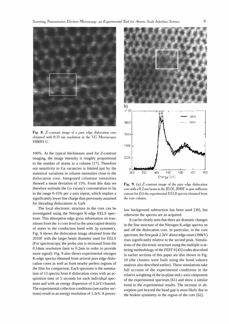
Fig. 8 shows a Z-contrast image obtained from theVG HB603 U dedicated STEM (the alignment, opera-tion and resolution of which is the same as the JEOL2010F described in earlier sections. The only differ-ence being that this instrument has a cold field emissiongun). The core clearly shows the eight-fold ring struc-ture, as previously reported [60]. On the basis of theprior theoretical calculations, this n-type sample grownunder N-rich growth conditions (The sample is alsodoped with Si at a level of ~ 2.1018 cm-3 and has a freecarrier mobility is about 200 cm2/Vs) is expected toshow a Ga-vacancy core structure [54]. Since atomscontribute to the image according to their mean squareatomic number (Z), the light N atoms contribute only5% of the image contrast in a full GaN atomic column.Thus it is immediately apparent from the image thatthe Ga vacancy concentration must be much less than
100%. At the typical thicknesses used for Z-contrastimaging, the image intensity is roughly proportionalto the number of atoms in a column [17]. Thereforeour sensitivity to Ga vacancies is limited just by thestatistical variations in column intensities close to thedislocation core. Integrated columnar intensitiesshowed a mean deviation of 15%. From this data wetherefore estimate the Ga vacancy concentration to liein the range 0-15% per c-axis repeat, which implies asignificantly lower line charge than previously assumedfor threading dislocations in GaN.
The local electronic structure in the core can beinvestigated using the Nitrogen K-edge EELS spec-trum. This absorption edge gives information on tran-sitions from the 1s core level to the unoccupied densityof states in the conduction band with 2p symmetry.Fig. 9 shows the dislocation image obtained from the2010F with the larger beam diameter used for EELS(For spectroscopy, the probe size is increased from the0.14nm resolution limit to 0.2nm in order to providemore signal). Fig. 9 also shows experimental nitrogenK-edge spectra obtained from several pure edge dislo-cation cores as well as from nearby perfect regions ofthe film for comparison. Each spectrum is the summa-tion of 13 spectra from 8 dislocation cores with an ac-quisition time of 5 seconds for each individual spec-trum and with an energy dispersion of 0.2eV/channel.The experimental collection conditions (see earlier sec-tions) result in an energy resolution of 1.2eV. A power-
law background subtraction has been used [30], butotherwise the spectra are as acquired.
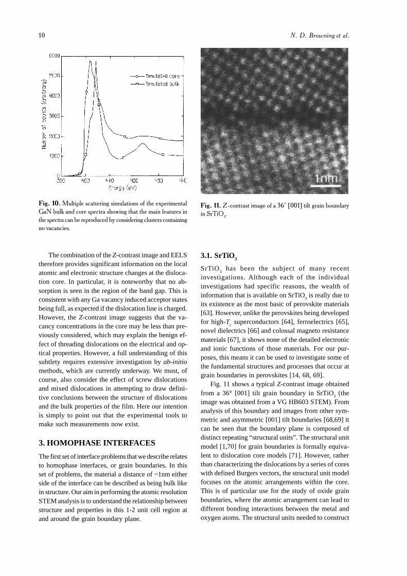
It can be clearly seen that there are dramatic changesin the fine structure of the Nitrogen K-edge spectra onand off the dislocation core. In particular, in the corespectrum, the first peak 2.2eV above edge onset (398eV)rises significantly relative to the second peak. Simula-tions of the electronic structure using the multiple scat-tering methodology of the FEFF 8 [43] codes describedin earlier sections of this paper are also shown in Fig.10 (the clusters were built using the bond valenceanalysis also described earlier). These simulations takefull account of the experimental conditions in therelative weighting of the in-plane and c-axis componentof the experimental spectrum [61] and show a similartrend to the experimental results. The increase in ab-sorption just beyond the band gap is most likely due tothe broken symmetry in the region of the core [62].
The combination of the Z-contrast image and EELStherefore provides significant information on the localatomic and electronic structure changes at the disloca-tion core. In particular, it is noteworthy that no ab-sorption is seen in the region of the band gap. This isconsistent with any Ga vacancy induced acceptor statesbeing full, as expected if the dislocation line is charged.However, the Z-contrast image suggests that the va-cancy concentrations in the core may be less than pre-viously considered, which may explain the benign ef-fect of threading dislocations on the electrical and op-tical properties. However, a full understanding of thissubtlety requires extensive investigation by ab-initiomethods, which are currently underway. We must, ofcourse, also consider the effect of screw dislocationsand mixed dislocations in attempting to draw defini-tive conclusions between the structure of dislocationsand the bulk properties of the film. Here our intentionis simply to point out that the experimental tools tomake such measurements now exist.
3. HOMOPHASE INTERFACES
The first set of interface problems that we describe relatesto homophase interfaces, or grain boundaries. In thisset of problems, the material a distance of ~1nm eitherside of the interface can be described as being bulk likein structure. Our aim in performing the atomic resolutionSTEM analysis is to understand the relationship betweenstructure and properties in this 1-2 unit cell region atand around the grain boundary plane.
3.1. SrTiO3
SrTiO3 has been the subject of many recent
investigations. Although each of the individualinvestigations had specific reasons, the wealth ofinformation that is available on SrTiO
3 is really due to
its existence as the most basic of perovskite materials[63]. However, unlike the perovskites being developedfor high-T
c superconductors [64], ferroelectrics [65],
novel dielectrics [66] and colossal magneto resistancematerials [67], it shows none of the detailed electronicand ionic functions of those materials. For our pur-poses, this means it can be used to investigate some ofthe fundamental structures and processes that occur atgrain boundaries in perovskites [14, 68, 69].
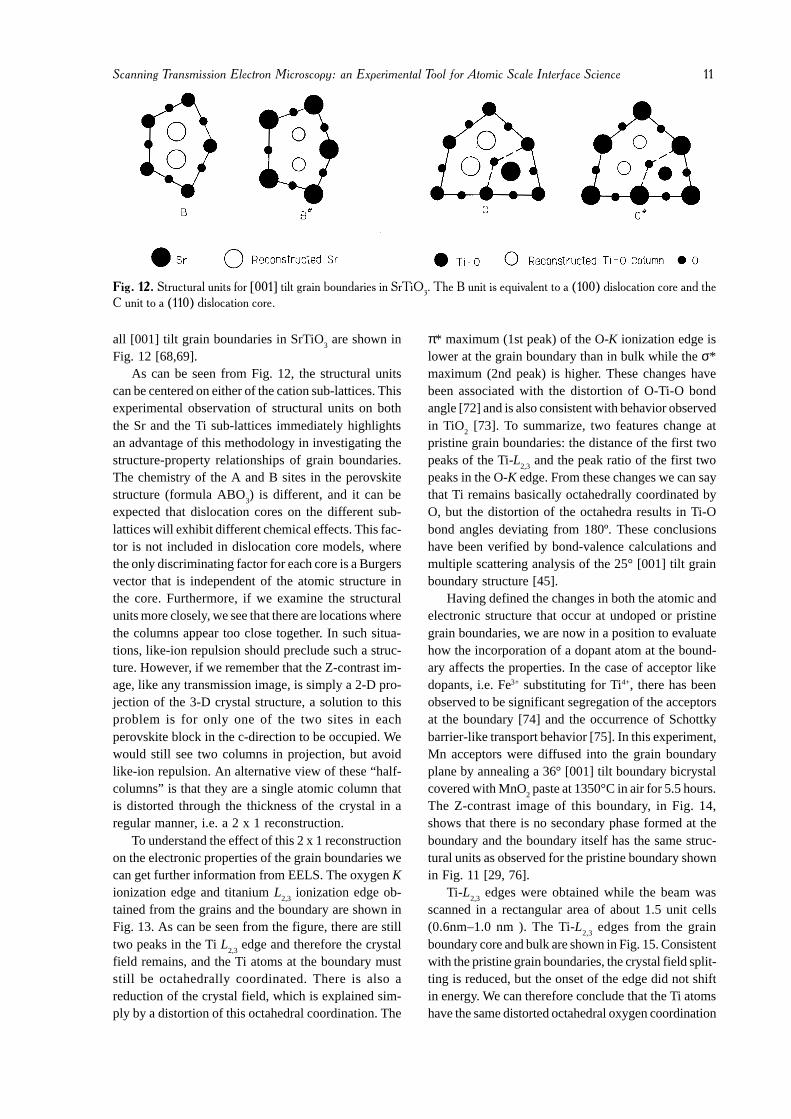
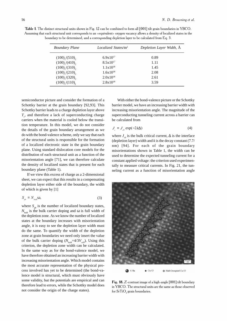
Fig. 11 shows a typical Z-contrast image obtainedfrom a 36° [001] tilt grain boundary in SrTiO3 (theimage was obtained from a VG HB603 STEM). Fromanalysis of this boundary and images from other sym-metric and asymmetric [001] tilt boundaries [68,69] itcan be seen that the boundary plane is composed ofdistinct repeating “structural units”. The structural unitmodel [1,70] for grain boundaries is formally equiva-lent to dislocation core models [71]. However, ratherthan characterizing the dislocations by a series of coreswith defined Burgers vectors, the structural unit modelfocuses on the atomic arrangements within the core.This is of particular use for the study of oxide grainboundaries, where the atomic arrangement can lead todifferent bonding interactions between the metal andoxygen atoms. The structural units needed to construct
all [001] tilt grain boundaries in SrTiO3 are shown in
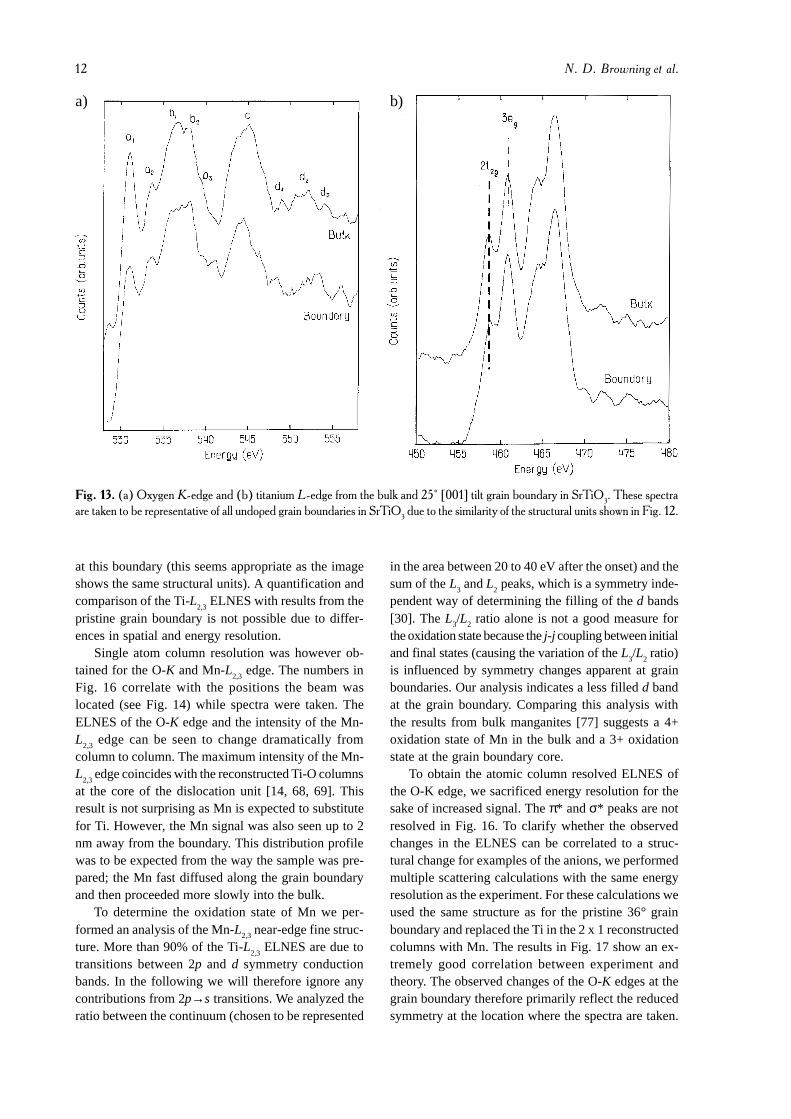
Fig. 12 [68,69].As can be seen from Fig. 12, the structural units
can be centered on either of the cation sub-lattices. Thisexperimental observation of structural units on boththe Sr and the Ti sub-lattices immediately highlightsan advantage of this methodology in investigating thestructure-property relationships of grain boundaries.The chemistry of the A and B sites in the perovskitestructure (formula ABO
3) is different, and it can be
expected that dislocation cores on the different sub-lattices will exhibit different chemical effects. This fac-tor is not included in dislocation core models, wherethe only discriminating factor for each core is a Burgersvector that is independent of the atomic structure inthe core. Furthermore, if we examine the structuralunits more closely, we see that there are locations wherethe columns appear too close together. In such situa-tions, like-ion repulsion should preclude such a struc-ture. However, if we remember that the Z-contrast im-age, like any transmission image, is simply a 2-D pro-jection of the 3-D crystal structure, a solution to thisproblem is for only one of the two sites in eachperovskite block in the c-direction to be occupied. Wewould still see two columns in projection, but avoidlike-ion repulsion. An alternative view of these “half-columns” is that they are a single atomic column thatis distorted through the thickness of the crystal in aregular manner, i.e. a 2 x 1 reconstruction.
To understand the effect of this 2 x 1 reconstructionon the electronic properties of the grain boundaries wecan get further information from EELS. The oxygen Kionization edge and titanium L
2,3 ionization edge ob-
tained from the grains and the boundary are shown inFig. 13. As can be seen from the figure, there are stilltwo peaks in the Ti L
2,3 edge and therefore the crystal
field remains, and the Ti atoms at the boundary muststill be octahedrally coordinated. There is also areduction of the crystal field, which is explained sim-ply by a distortion of this octahedral coordination. The
π* maximum (1st peak) of the O-K ionization edge islower at the grain boundary than in bulk while the σ*maximum (2nd peak) is higher. These changes havebeen associated with the distortion of O-Ti-O bondangle [72] and is also consistent with behavior observedin TiO
2 [73]. To summarize, two features change at
pristine grain boundaries: the distance of the first twopeaks of the Ti-L
2,3 and the peak ratio of the first two
peaks in the O-K edge. From these changes we can saythat Ti remains basically octahedrally coordinated byO, but the distortion of the octahedra results in Ti-Obond angles deviating from 180º. These conclusionshave been verified by bond-valence calculations andmultiple scattering analysis of the 25° [001] tilt grainboundary structure [45].
Having defined the changes in both the atomic andelectronic structure that occur at undoped or pristinegrain boundaries, we are now in a position to evaluatehow the incorporation of a dopant atom at the bound-ary affects the properties. In the case of acceptor likedopants, i.e. Fe3+ substituting for Ti4+, there has beenobserved to be significant segregation of the acceptorsat the boundary [74] and the occurrence of Schottkybarrier-like transport behavior [75]. In this experiment,Mn acceptors were diffused into the grain boundaryplane by annealing a 36° [001] tilt boundary bicrystalcovered with MnO
2 paste at 1350°C in air for 5.5 hours.
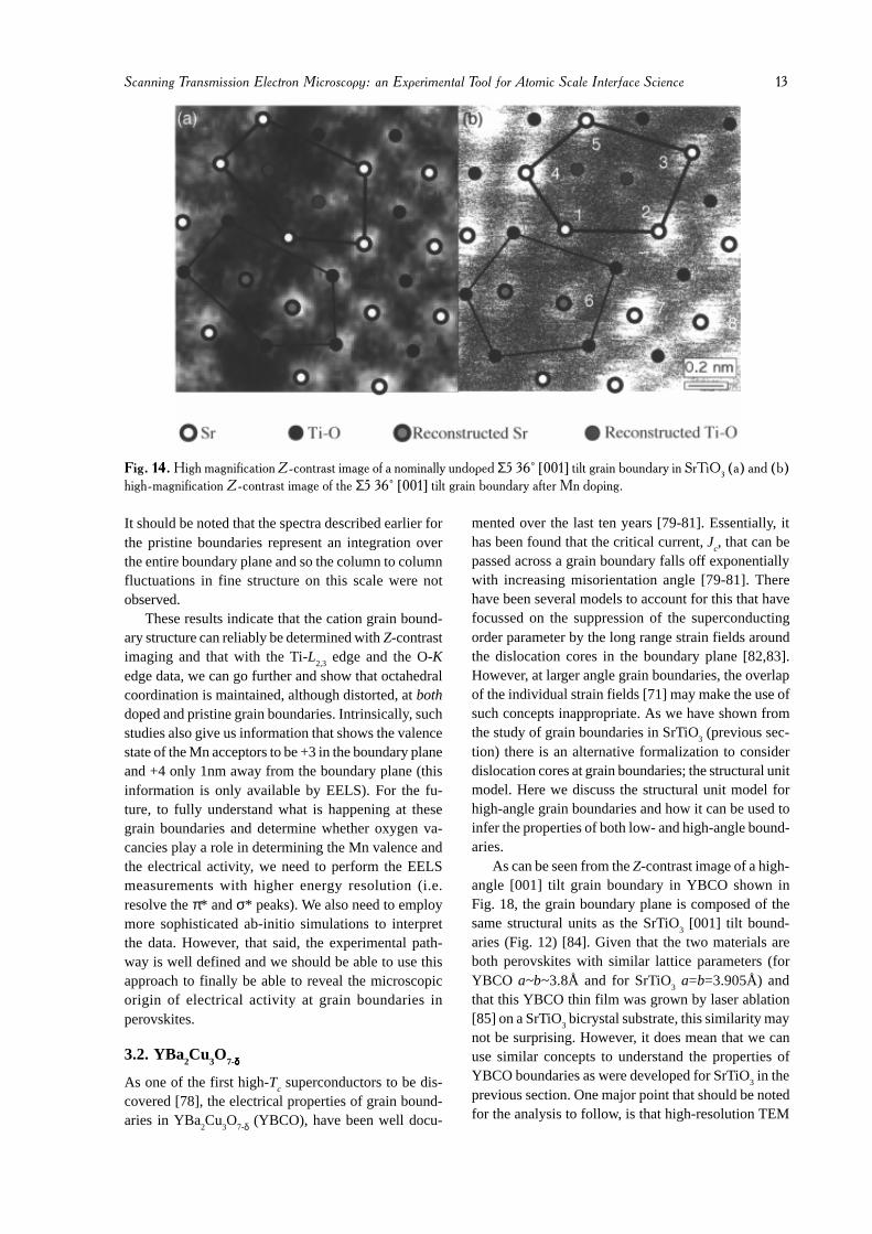
The Z-contrast image of this boundary, in Fig. 14,shows that there is no secondary phase formed at theboundary and the boundary itself has the same struc-tural units as observed for the pristine boundary shownin Fig. 11 [29, 76].
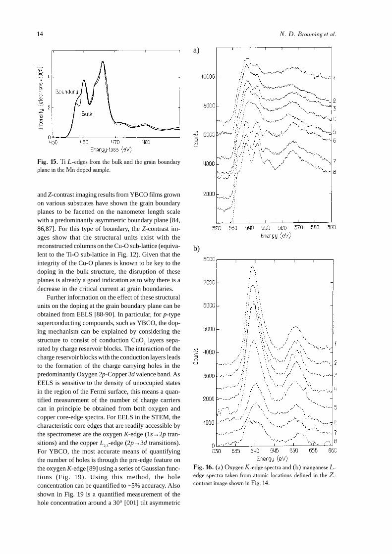
Ti-L2,3
edges were obtained while the beam wasscanned in a rectangular area of about 1.5 unit cells(0.6nm–1.0 nm ). The Ti-L
2,3 edges from the grain
boundary core and bulk are shown in Fig. 15. Consistentwith the pristine grain boundaries, the crystal field split-ting is reduced, but the onset of the edge did not shiftin energy. We can therefore conclude that the Ti atomshave the same distorted octahedral oxygen coordination
at this boundary (this seems appropriate as the imageshows the same structural units). A quantification andcomparison of the Ti-L
2,3 ELNES with results from the
pristine grain boundary is not possible due to differ-ences in spatial and energy resolution.
Single atom column resolution was however ob-tained for the O-K and Mn-L
2,3 edge. The numbers in
Fig. 16 correlate with the positions the beam waslocated (see Fig. 14) while spectra were taken. TheELNES of the O-K edge and the intensity of the Mn-L
2,3 edge can be seen to change dramatically from
column to column. The maximum intensity of the Mn-L
2,3 edge coincides with the reconstructed Ti-O columns
at the core of the dislocation unit [14, 68, 69]. Thisresult is not surprising as Mn is expected to substitutefor Ti. However, the Mn signal was also seen up to 2nm away from the boundary. This distribution profilewas to be expected from the way the sample was pre-pared; the Mn fast diffused along the grain boundaryand then proceeded more slowly into the bulk.
To determine the oxidation state of Mn we per-formed an analysis of the Mn-L2,3 near-edge fine struc-ture. More than 90% of the Ti-L
2,3 ELNES are due to
transitions between 2p and d symmetry conductionbands. In the following we will therefore ignore anycontributions from 2p→s transitions. We analyzed theratio between the continuum (chosen to be represented
in the area between 20 to 40 eV after the onset) and thesum of the L
3 and L
2 peaks, which is a symmetry inde-
pendent way of determining the filling of the d bands[30]. The L3/L2 ratio alone is not a good measure forthe oxidation state because the j-j coupling between initialand final states (causing the variation of the L
3/L
2 ratio)
is influenced by symmetry changes apparent at grainboundaries. Our analysis indicates a less filled d bandat the grain boundary. Comparing this analysis withthe results from bulk manganites [77] suggests a 4+oxidation state of Mn in the bulk and a 3+ oxidationstate at the grain boundary core.
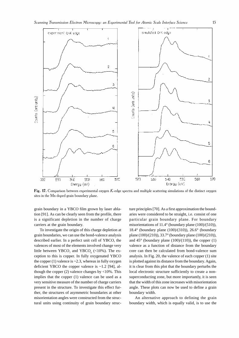
To obtain the atomic column resolved ELNES ofthe O-K edge, we sacrificed energy resolution for thesake of increased signal. The π* and σ* peaks are notresolved in Fig. 16. To clarify whether the observedchanges in the ELNES can be correlated to a struc-tural change for examples of the anions, we performedmultiple scattering calculations with the same energyresolution as the experiment. For these calculations weused the same structure as for the pristine 36° grainboundary and replaced the Ti in the 2 x 1 reconstructedcolumns with Mn. The results in Fig. 17 show an ex-tremely good correlation between experiment andtheory. The observed changes of the O-K edges at thegrain boundary therefore primarily reflect the reducedsymmetry at the location where the spectra are taken.
It should be noted that the spectra described earlier forthe pristine boundaries represent an integration overthe entire boundary plane and so the column to columnfluctuations in fine structure on this scale were notobserved.
These results indicate that the cation grain bound-ary structure can reliably be determined with Z-contrastimaging and that with the Ti-L
2,3 edge and the O-K
edge data, we can go further and show that octahedralcoordination is maintained, although distorted, at bothdoped and pristine grain boundaries. Intrinsically, suchstudies also give us information that shows the valencestate of the Mn acceptors to be +3 in the boundary planeand +4 only 1nm away from the boundary plane (thisinformation is only available by EELS). For the fu-ture, to fully understand what is happening at thesegrain boundaries and determine whether oxygen va-cancies play a role in determining the Mn valence andthe electrical activity, we need to perform the EELSmeasurements with higher energy resolution (i.e.resolve the π* and σ* peaks). We also need to employmore sophisticated ab-initio simulations to interpretthe data. However, that said, the experimental path-way is well defined and we should be able to use thisapproach to finally be able to reveal the microscopicorigin of electrical activity at grain boundaries inperovskites.
3.2. YBa2Cu3O7-δδδδδ
As one of the first high-Tc superconductors to be dis-
covered [78], the electrical properties of grain bound-aries in YBa
mented over the last ten years [79-81]. Essentially, ithas been found that the critical current, J
c, that can be
passed across a grain boundary falls off exponentiallywith increasing misorientation angle [79-81]. Therehave been several models to account for this that havefocussed on the suppression of the superconductingorder parameter by the long range strain fields aroundthe dislocation cores in the boundary plane [82,83].However, at larger angle grain boundaries, the overlapof the individual strain fields [71] may make the use ofsuch concepts inappropriate. As we have shown fromthe study of grain boundaries in SrTiO
3 (previous sec-
tion) there is an alternative formalization to considerdislocation cores at grain boundaries; the structural unitmodel. Here we discuss the structural unit model forhigh-angle grain boundaries and how it can be used toinfer the properties of both low- and high-angle bound-aries.
As can be seen from the Z-contrast image of a high-angle [001] tilt grain boundary in YBCO shown inFig. 18, the grain boundary plane is composed of thesame structural units as the SrTiO
3 [001] tilt bound-
aries (Fig. 12) [84]. Given that the two materials areboth perovskites with similar lattice parameters (forYBCO a~b~3.8Å and for SrTiO
3 a=b=3.905Å) and
that this YBCO thin film was grown by laser ablation[85] on a SrTiO
3 bicrystal substrate, this similarity may
not be surprising. However, it does mean that we canuse similar concepts to understand the properties ofYBCO boundaries as were developed for SrTiO
3 in the
previous section. One major point that should be notedfor the analysis to follow, is that high-resolution TEM
�! ��������������������
and Z-contrast imaging results from YBCO films grownon various substrates have shown the grain boundaryplanes to be facetted on the nanometer length scalewith a predominantly asymmetric boundary plane [84,86,87]. For this type of boundary, the Z-contrast im-ages show that the structural units exist with thereconstructed columns on the Cu-O sub-lattice (equiva-lent to the Ti-O sub-lattice in Fig. 12). Given that theintegrity of the Cu-O planes is known to be key to thedoping in the bulk structure, the disruption of theseplanes is already a good indication as to why there is adecrease in the critical current at grain boundaries.
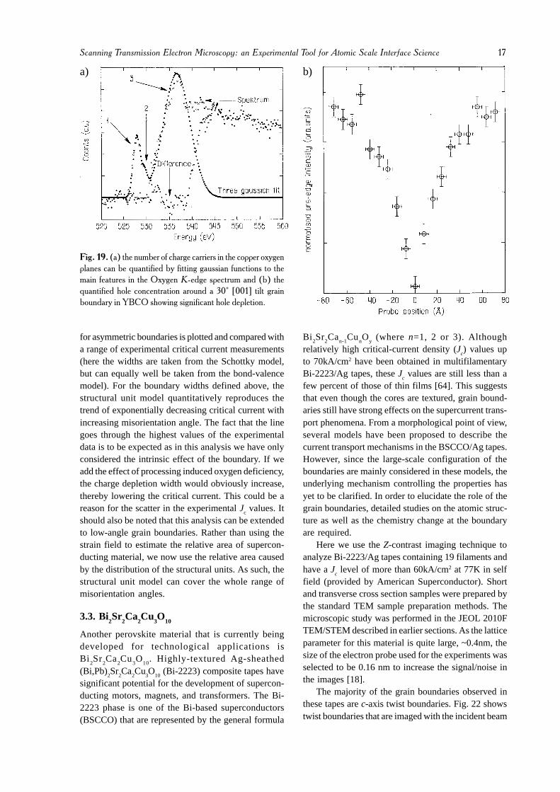
Further information on the effect of these structuralunits on the doping at the grain boundary plane can beobtained from EELS [88-90]. In particular, for p-typesuperconducting compounds, such as YBCO, the dop-ing mechanism can be explained by considering thestructure to consist of conduction CuO2 layers sepa-rated by charge reservoir blocks. The interaction of thecharge reservoir blocks with the conduction layers leadsto the formation of the charge carrying holes in thepredominantly Oxygen 2p-Copper 3d valence band. AsEELS is sensitive to the density of unoccupied statesin the region of the Fermi surface, this means a quan-tified measurement of the number of charge carrierscan in principle be obtained from both oxygen andcopper core-edge spectra. For EELS in the STEM, thecharacteristic core edges that are readily accessible bythe spectrometer are the oxygen K-edge (1s→2p tran-sitions) and the copper L2,3-edge (2p→3d transitions).For YBCO, the most accurate means of quantifyingthe number of holes is through the pre-edge feature onthe oxygen K-edge [89] using a series of Gaussian func-tions (Fig. 19). Using this method, the holeconcentration can be quantified to ~5% accuracy. Alsoshown in Fig. 19 is a quantified measurement of thehole concentration around a 30° [001] tilt asymmetric
grain boundary in a YBCO film grown by laser abla-tion [91]. As can be clearly seen from the profile, thereis a significant depletion in the number of chargecarriers at the grain boundary.
To investigate the origin of this charge depletion atgrain boundaries, we can use the bond-valence analysisdescribed earlier. In a perfect unit cell of YBCO, thevalences of most of the elements involved change verylittle between YBCO
7 and YBCO
6 (<10%). The ex-
ception to this is copper. In fully oxygenated YBCOthe copper (1) valence is ~2.3, whereas in fully oxygendeficient YBCO the copper valence is ~1.2 [94], al-though the copper (2) valence changes by <10%. Thisimplies that the copper (1) valence can be used as avery sensitive measure of the number of charge carrierspresent in the structure. To investigate this effect fur-ther, the structures of asymmetric boundaries at othermisorientation angles were constructed from the struc-tural units using continuity of grain boundary struc-
ture principles [70]. As a first approximation the bound-aries were considered to be straight, i.e. consist of oneparticular grain boundary plane. For boundarymisorientations of 11.4° (boundary plane (100)/(510)),18.4° (boundary plane (100)/(310)), 26.6° (boundaryplane (100)/(210)), 33.7° (boundary plane (100)/(210)),and 45° (boundary plane (100)/(110)), the copper (1)valence as a function of distance from the boundarycore can then be calculated from bond-valence sumanalysis. In Fig. 20, the valence of each copper (1) siteis plotted against its distance from the boundary. Again,it is clear from this plot that the boundary perturbs thelocal electronic structure sufficiently to create a non-superconducting zone, but more importantly, it is seenthat the width of this zone increases with misorientationangle. These plots can now be used to define a grainboundary width.
An alternative approach to defining the grainboundary width, which is equally valid, is to use the
semiconductor picture and consider the formation of aSchottky barrier at the grain boundary [92,93]. ThisSchottky barrier leads to a charge depletion layer aboveT
c, and therefore a lack of superconducting charge
carriers when the material is cooled below the transi-tion temperature. In this model, we do not considerthe details of the grain boundary arrangement as wedo with the bond-valence scheme, only we say that eachof the structural units is responsible for the formationof a localized electronic state in the grain boundaryplane. Using standard dislocation core models for thedistribution of each structural unit as a function of themisorientation angle [71], we can therefore calculatethe density of localized states that is present for eachboundary plane (Table 1).
If we view this excess of charge as a 2-dimensionalsheet, we can expect that this results in a compensatingdepletion layer either side of the boundary, the widthof which is given by [1]
� � ��
= ω (3)
where Sgb
is the number of localized boundary states,N
bulk is the bulk carrier doping and ω is full width of
the depletion zone. As we know the number of localizedstates at the boundary increases with misorientationangle, it is easy to see the depletion layer width mustdo the same. To quantify the width of the depletionzone at grain boundaries we need only insert the valueof the bulk carrier doping (N
bulk=4/3V
cell). Using this
criterion, the depletion zone width can be calculated.In the same way as for the bond-valence model, wehave therefore obtained an increasing barrier width withincreasing misorientation angle. Which model containsthe most accurate representation of the physical pro-cess involved has yet to be determined (the bond-va-lence model is structural, which must obviously havesome validity, but the potentials are empirical and cantherefore lead to errors, while the Schottky model doesnot consider the origin of the charge states).
With either the bond-valence picture or the Schottkybarrier model, we have an increasing barrier width withincreasing misorientation angle. The magnitude of thesuperconducting tunneling current across a barrier canbe calculated from
� � � �
= −�
����� �∆ (4)
where Jc0
is the bulk critical current, ∆ is the interface(depletion layer) width and k is the decay constant (7.7/nm) [94]. For each of the grain boundarymisorientations shown in Table 1, the width can beused to determine the expected tunneling current for aconstant applied voltage: the criterion used experimen-tally to measure critical currents. In Fig. 21, the tun-neling current as a function of misorientation angle
for asymmetric boundaries is plotted and compared witha range of experimental critical current measurements(here the widths are taken from the Schottky model,but can equally well be taken from the bond-valencemodel). For the boundary widths defined above, thestructural unit model quantitatively reproduces thetrend of exponentially decreasing critical current withincreasing misorientation angle. The fact that the linegoes through the highest values of the experimentaldata is to be expected as in this analysis we have onlyconsidered the intrinsic effect of the boundary. If weadd the effect of processing induced oxygen deficiency,the charge depletion width would obviously increase,thereby lowering the critical current. This could be areason for the scatter in the experimental J
c values. It
should also be noted that this analysis can be extendedto low-angle grain boundaries. Rather than using thestrain field to estimate the relative area of supercon-ducting material, we now use the relative area causedby the distribution of the structural units. As such, thestructural unit model can cover the whole range ofmisorientation angles.
3.3. Bi2Sr
2Ca
2Cu
3O
10
Another perovskite material that is currently beingdeveloped for technological applications isBi
2Sr
2Ca
2Cu
3O
10. Highly-textured Ag-sheathed
(Bi,Pb)2Sr
2Ca
2Cu
3O
10 (Bi-2223) composite tapes have
significant potential for the development of supercon-ducting motors, magnets, and transformers. The Bi-2223 phase is one of the Bi-based superconductors(BSCCO) that are represented by the general formula
Bi2Sr2Can-1CunOy (where n=1, 2 or 3). Althoughrelatively high critical-current density (J
c) values up
to 70kA/cm2 have been obtained in multifilamentaryBi-2223/Ag tapes, these J
c values are still less than a
few percent of those of thin films [64]. This suggeststhat even though the cores are textured, grain bound-aries still have strong effects on the supercurrent trans-port phenomena. From a morphological point of view,several models have been proposed to describe thecurrent transport mechanisms in the BSCCO/Ag tapes.However, since the large-scale configuration of theboundaries are mainly considered in these models, theunderlying mechanism controlling the properties hasyet to be clarified. In order to elucidate the role of thegrain boundaries, detailed studies on the atomic struc-ture as well as the chemistry change at the boundaryare required.
Here we use the Z-contrast imaging technique toanalyze Bi-2223/Ag tapes containing 19 filaments andhave a J
c level of more than 60kA/cm2 at 77K in self
field (provided by American Superconductor). Shortand transverse cross section samples were prepared bythe standard TEM sample preparation methods. Themicroscopic study was performed in the JEOL 2010FTEM/STEM described in earlier sections. As the latticeparameter for this material is quite large, ~0.4nm, thesize of the electron probe used for the experiments wasselected to be 0.16 nm to increase the signal/noise inthe images [18].
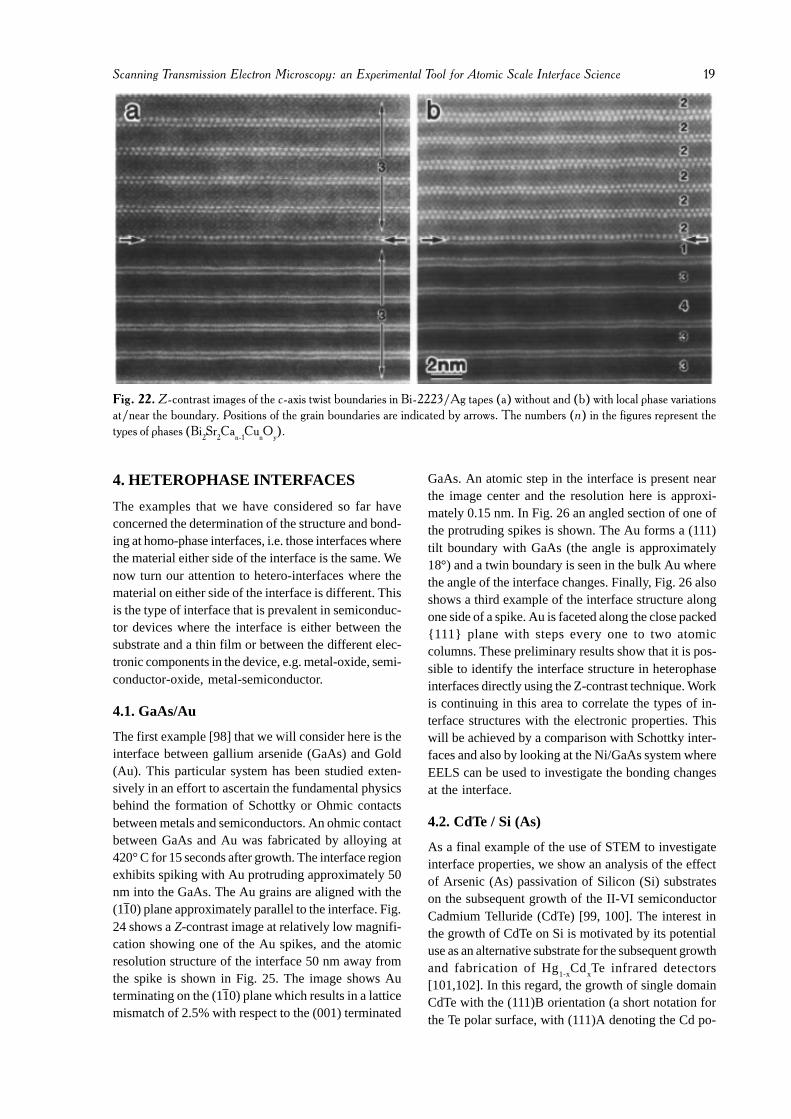
The majority of the grain boundaries observed inthese tapes are c-axis twist boundaries. Fig. 22 showstwist boundaries that are imaged with the incident beam
a) b)
�: ��������������������
oriented parallel to the [110] direction in the upperhalf of the images. In the lower half several sets of twobright lines are observed which correspond to the BiOdouble layers viewed end on. From these images it isquite obvious that the boundary is atomically flat andlocated in the middle of the double BiO layers. Suchresults are consistent with previous conventional high-resolution TEM images [95], but the advantage of Z-contrast imaging is that the nature and the location ofthe boundary can be directly identified from the rawimages without simulation. Another key point fromthese images is that although no amorphous layers areobserved at the boundaries, local phase variations areoften observed (the lack of a phase variation shown inFig. 22 (a) is actually the minority case). In Fig. 22 (b)three unit cells of Bi-2212 phase are observed on theupper side of the boundary and a half unit cell of Bi-2201 phase on the lower part are present (T
c=20K as
opposed to 110K for Bi-2223). Also, in the lower partof the image a half unit cell of the Bi-2234 phase isseen near the boundary. Both the type and number ofphases formed at/near the boundary is found to varyfrom boundary to boundary. Such local phase varia-tions at/near the boundary should have a stronginfluence on the local transport phenomena of the su-percurrent as the thickness of the secondary phases istypically larger than the coherence length, especiallyin the framework of the brick-wall model [96].
Another typical set of grain boundaries usuallypresent in BSCCO/Ag tapes is small-angle c-axis tiltboundaries. A characteristic of this type of the bound-
ary is that basal planes of one grain are parallel to thegrain boundary plane. This type of boundary has beenconsidered to play a dominant role in transporting thesupercurrent in the railway-switch model [97]. Fig. 23shows an 11° tilt boundary imaged with the incidentbeam oriented parallel to [110] orientation of eachgrain. These two images were obtained from the samearea (there is a slight mis-tilt precludes imaging bothgrains simultaneously). Periodic formation of the n=1,2, 3 and 4 phases in upper grain and n=2 and 3 in thelower grain is observed along the boundary. Since theangle between the [110] of both grains is less than 0.1°,a grain boundary structure can be constructed fromthese two images. Fig. 23 shows a schematic diagramof the grain boundary structure. In this figure, we cansee again that the boundary forms on the BiO layersand that the type of phase formed varies periodicallyalong the boundary. We should also note that this peri-odic formation of different phases at the boundaries isalso observed at small-angle c-axis tilt boundaries witha twist component. These different phases are expectedto have different transport properties and the periodiclocal formation of different phases along a grain bound-ary plane may have important effects on the supercur-rent transport not only through c-axis twist boundariesbut also through small c-axis tilt boundaries, i.e. weaklinks are formed.
The examples that we have considered so far haveconcerned the determination of the structure and bond-ing at homo-phase interfaces, i.e. those interfaces wherethe material either side of the interface is the same. Wenow turn our attention to hetero-interfaces where thematerial on either side of the interface is different. Thisis the type of interface that is prevalent in semiconduc-tor devices where the interface is either between thesubstrate and a thin film or between the different elec-tronic components in the device, e.g. metal-oxide, semi-conductor-oxide, metal-semiconductor.
4.1. GaAs/Au
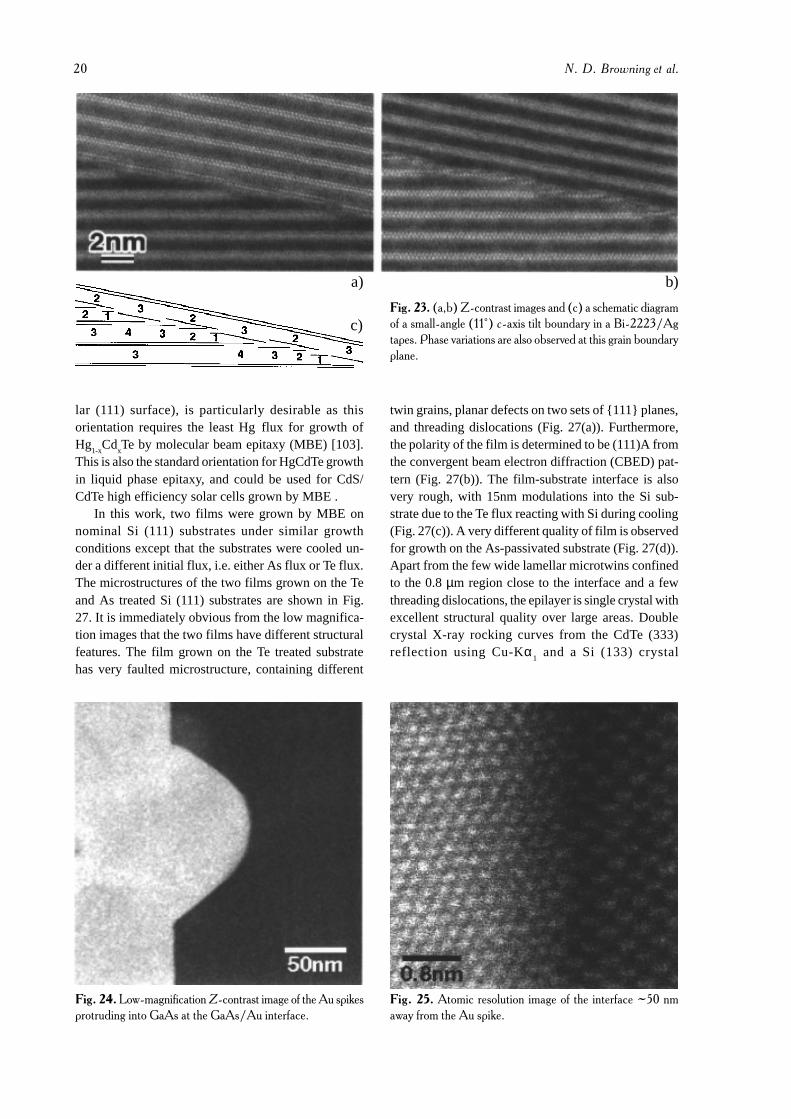
The first example [98] that we will consider here is theinterface between gallium arsenide (GaAs) and Gold(Au). This particular system has been studied exten-sively in an effort to ascertain the fundamental physicsbehind the formation of Schottky or Ohmic contactsbetween metals and semiconductors. An ohmic contactbetween GaAs and Au was fabricated by alloying at420° C for 15 seconds after growth. The interface regionexhibits spiking with Au protruding approximately 50nm into the GaAs. The Au grains are aligned with the(110) plane approximately parallel to the interface. Fig.24 shows a Z-contrast image at relatively low magnifi-cation showing one of the Au spikes, and the atomicresolution structure of the interface 50 nm away fromthe spike is shown in Fig. 25. The image shows Auterminating on the (110) plane which results in a latticemismatch of 2.5% with respect to the (001) terminated
GaAs. An atomic step in the interface is present nearthe image center and the resolution here is approxi-mately 0.15 nm. In Fig. 26 an angled section of one ofthe protruding spikes is shown. The Au forms a (111)tilt boundary with GaAs (the angle is approximately18°) and a twin boundary is seen in the bulk Au wherethe angle of the interface changes. Finally, Fig. 26 alsoshows a third example of the interface structure alongone side of a spike. Au is faceted along the close packed{111} plane with steps every one to two atomiccolumns. These preliminary results show that it is pos-sible to identify the interface structure in heterophaseinterfaces directly using the Z-contrast technique. Workis continuing in this area to correlate the types of in-terface structures with the electronic properties. Thiswill be achieved by a comparison with Schottky inter-faces and also by looking at the Ni/GaAs system whereEELS can be used to investigate the bonding changesat the interface.
4.2. CdTe / Si (As)
As a final example of the use of STEM to investigateinterface properties, we show an analysis of the effectof Arsenic (As) passivation of Silicon (Si) substrateson the subsequent growth of the II-VI semiconductorCadmium Telluride (CdTe) [99, 100]. The interest inthe growth of CdTe on Si is motivated by its potentialuse as an alternative substrate for the subsequent growthand fabrication of Hg
1-xCd
xTe infrared detectors
[101,102]. In this regard, the growth of single domainCdTe with the (111)B orientation (a short notation forthe Te polar surface, with (111)A denoting the Cd po-
lar (111) surface), is particularly desirable as thisorientation requires the least Hg flux for growth ofHg
1-xCd
xTe by molecular beam epitaxy (MBE) [103].
This is also the standard orientation for HgCdTe growthin liquid phase epitaxy, and could be used for CdS/CdTe high efficiency solar cells grown by MBE .
In this work, two films were grown by MBE onnominal Si (111) substrates under similar growthconditions except that the substrates were cooled un-der a different initial flux, i.e. either As flux or Te flux.The microstructures of the two films grown on the Teand As treated Si (111) substrates are shown in Fig.27. It is immediately obvious from the low magnifica-tion images that the two films have different structuralfeatures. The film grown on the Te treated substratehas very faulted microstructure, containing different
twin grains, planar defects on two sets of {111} planes,and threading dislocations (Fig. 27(a)). Furthermore,the polarity of the film is determined to be (111)A fromthe convergent beam electron diffraction (CBED) pat-tern (Fig. 27(b)). The film-substrate interface is alsovery rough, with 15nm modulations into the Si sub-strate due to the Te flux reacting with Si during cooling(Fig. 27(c)). A very different quality of film is observedfor growth on the As-passivated substrate (Fig. 27(d)).Apart from the few wide lamellar microtwins confinedto the 0.8 µm region close to the interface and a fewthreading dislocations, the epilayer is single crystal withexcellent structural quality over large areas. Doublecrystal X-ray rocking curves from the CdTe (333)reflection using Cu-Kα
monochromater gives measurement of the full widthat half maximum (FWHM) of 87 arcseconds for a 5 µmthick layer. The selected area diffraction pattern fromthe CdTe/Si interface shows the perfect alignment ofCdTe (111) layer relative to the Si (111) substrate (Fig.27(e)). The polarity of the film is confirmed to be (111)Bby CBED(Fig. 27(f)). We should note at this point thatthis initial analysis of the general film microstructureshighlights one of the advantages of the modern TEM/STEM instruments, i.e. that you can perform detailedphase contrast imaging and diffraction work in TEMmode prior to the more detailed STEM analysis.
The difference in the quality of the films thereforeappears to be related to the difference in the initial fluxtreatment of the Si (111) surface. Examining the CdTe/
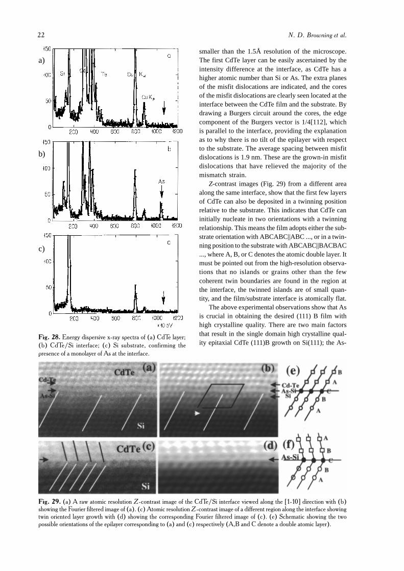
Si interface by energy dispersive X-ray spectroscopy(EDS) shows that the As that is initially deposited onthe Si surface remains there for the subsequent growthof the CdTe film (Fig. 28). The three spectra show thatonly when the 1nm probe is placed at the interface isthere an As signal present (the two other spectra areobtained ~5 nm from the interface). Furthermore, quan-tifying the spectra shown in Fig. 8 gives an estimate ofthe As concentration close to one monolayer. Theseresults are consistent with the in situ reflection highenergy electron diffraction (RHEED) observations be-fore initiation of the CdTe growth, and confirmed byx-ray photoemission spectroscopy [104].
Having generated a general picture of the filmmorphology and the composition of the film-substrateinterface we can now move on to examine the inter-face in more detail using atomic resolution Z-contrastimaging. Fig. 29 shows a raw atomic resolution Z-contrast image of the CdTe/Si interface, and the sameimage after Fourier filtering. The elongated white spotsin the image are atomic columns separated by distances
smaller than the 1.5Å resolution of the microscope.The first CdTe layer can be easily ascertained by theintensity difference at the interface, as CdTe has ahigher atomic number than Si or As. The extra planesof the misfit dislocations are indicated, and the coresof the misfit dislocations are clearly seen located at theinterface between the CdTe film and the substrate. Bydrawing a Burgers circuit around the cores, the edgecomponent of the Burgers vector is 1/4[112], whichis parallel to the interface, providing the explanationas to why there is no tilt of the epilayer with respectto the substrate. The average spacing between misfitdislocations is 1.9 nm. These are the grown-in misfitdislocations that have relieved the majority of themismatch strain.
Z-contrast images (Fig. 29) from a different areaalong the same interface, show that the first few layersof CdTe can also be deposited in a twinning positionrelative to the substrate. This indicates that CdTe caninitially nucleate in two orientations with a twinningrelationship. This means the film adopts either the sub-strate orientation with ABCABC||ABC ..., or in a twin-ning position to the substrate with ABCABC||BACBAC..., where A, B, or C denotes the atomic double layer. Itmust be pointed out from the high-resolution observa-tions that no islands or grains other than the fewcoherent twin boundaries are found in the region atthe interface, the twinned islands are of small quan-tity, and the film/substrate interface is atomically flat.
The above experimental observations show that Asis crucial in obtaining the desired (111) B film withhigh crystalline quality. There are two main factorsthat result in the single domain high crystalline qual-ity epitaxial CdTe (111)B growth on Si(111); the As-
passivated Si(111) surface which results in the (111) Bpolarity and the nature of atomic steps and terraces onthe nominally Si(111) surface which give rise to layergrowth free of multi-domains [99]. It is well knownthat As replaces the outermost Si atoms of the doublelayer during passivation of the Si(111) surface in theMBE growth process [105], and it is known from theabove investigations that As stays there after thegrowth. Both imply that As is present at the interfaceas a monolayer separating CdTe and Si during thegrowth. Based on the As-Cd, As-Te bond formationenergies [106], it is likely that Cd is favored as the firstatomic layer forming bond with the As at the inter-face, where the bonding configuration proceeds in afashion such as Si-As-Cd-Te across the interface asshown in Fig. 30.
Even though it is known that Cd atoms have a verylow sticking coefficient and would re-evaporate fromthe surface under only a Cd flux, the resultant CdTe(111) B layer growth implies that the presence of Teatoms supplied by stoichiometric flux is sufficient tostabilize the Cd on the surface. This occurs through atransition layer at the growth front. CdTe is initiatedwith Cd atoms forming one bond with As and three
bonds with Te, producing a Te stabilized growth sur-face, which finally results in the (111) B growth. Be-cause of the high interfacial energy associated with thelarge lattice mismatch between CdTe and Si and therequirement of low temperature initiation, layer depo-sition starts with island nucleation. CdTe nucleationcould initiate both at step edges and on the terraces,and because the atomic structures of the Si (111) sur-face comprise double layer steps giving the same atomicconfiguration from terrace to terrace, all the nucleiwould have only two possible positions, i.e. the twin-ing positions. In this system, the associated latticemismatch energy is the same for the two possible depo-sitions. However, the twinning position nuclei mighthave a higher interfacial energy due to the “faulted”stacking sequence across the interface, and thereforethe majority of the nuclei would adopt the orientationof the substrate (as is observed experimentally). Growththen proceeds in layer by layer fashion soon when thesubstrate temperature is raised to normal growth tem-perature after several tens of monolayer deposition.Because there is no tilt between the nucleating islands,the coherent double positioning boundaries are easilyeliminated after a short nucleation stage.
5. CONCLUSIONS
The ability to perform detailed atomic scale analysesof interfaces using correlated Z-contrast imaging andEELS is now well established on commercially avail-able microscopes. The further addition of other tech-niques, such as EDS, CBED and phase contrast imag-ing, will further enhance the level of characterizationpossible in the future. Such information allows us tobegin to unravel the complexities of the structure,composition and bonding changes that can occur atinterfaces and from that, develop a fundamental un-derstanding of the structure-property relationships. Formany materials systems currently being developed, thiscan provide the pathway to the realization of new tech-nologies.
ACKNOWLEDGMENTS
Aspects of this work were performed in collaborationwith S. Sivananthan, S. Rujiwarat, P. D. Nellist, V. P.Dravid, K. D. Johnson, R. P. Rodrigues, F. Omnés, B.Beaumont, J. P. Faurie, P. Gibart, J. L. Reno and A. G.Baca. The microscope facilities at UIC were purchasedwith support from the NSF under grant number DMR-9601792. Research performed on the semiconductorsystems was supported by NSF under grant numberDMR-9733895, research on the superconductors wassupported by NSF under grant number DMR-9803021,
grant number DE-FG02-996ER45610. This researchwas also supported in part by contract number DE-AC05-96OR22464 with Lockheed Martin Energy Sys-tems.
REFERENCES
[1] A. P. Sutton and R. W. Balluffi, Interfaces inCrystalline Materials (Oxford University Press,1995).
[2] See for example, Materials Interfaces, ed. by D.Wolf and S. Yip (Chapman & Hall, 1992).
[3] D. A. Muller, D. A. Sashkov, R. Benedek, L. H.Yang , J. Silcox and D. N. Seidman // Phys. Rev.Letts. 80 (1998) 4741.
[4] A. Zalar, B. M. M. Baretzky, S. Hofmann, M.Ruhle and P. Panjan // Thin Solid Films 352(1999) 151.
[5] R. Benedek, D. N. Seidman and L. H. Yang //Microscopy and Microanalysis 3 (1997) 333.
[6] D. A. Muller, T. Sorsch, S. Moccio, F. H.Baumann, K. Evans-Lutterodt and G. Timp //Nature 399 (1999) 758.
[7] G. Duscher, S. J. Pennycook, N. D. Browning, R.Rupangudi, C. Takoudis, H. J. Gao and R. Singh,In: proceedings of Characterization and Metrol-ogy for ULSI Technology: 1998 InternationalConference, ed. by D. G. Seiler, A. C. Deibold,W. M. Bullis, T. J. Shaffner, R. McDonald and E.J. Walters (American Institute of Physics, 1998)
[8] D. A. Muller, Y. Tzou, R. Raj and J. Silcox //Nature 366 (1993) 725.
[9] H. Hasegawa, Y. Koyama and T. Hashizume //Japanese Journal of Applied Physics 1 38 (1999)2634.
[10] F. Ernst, O. Keinzle and M. Ruhle // J. Eur.Ceram. Soc. 19 (1998) 665.
[11] M. F. Chisholm, A. Maiti, S. J. Pennycook andS. T. Pantelides // Phys. Rev. Letts. 81 (1998)132.
[12] D. A. Muller // Phys. Rev. B 58 (1998) 5989.[13] K. L. Merkle and D. J. Smith // Phys. Rev. Lett.
59 (1987) 2887.[14] M. M. McGibbon, N. D. Browning, M. F.
Chisholm, A. J. McGibbon, S. J. Pennycook, V.Ravikumar and V. P. Dravid // Science 266(1994) 102.
[15] S. J. Pennycook and L. A. Boatner // Nature 336(1988) 565.
[16] N. D. Browning, M. F. Chisholm and S. J.Pennycook // Nature 366 (1993) 143.
[17] P. D. Nellist and S. J. Pennycook // Ultramicros-copy 78 (1999) 111.
[18] E. M. James and N. D. Browning // Ultrami-croscopy 78 (1999) 125.
[19] E. M. James, N. D. Browning, A. W. Nicholls,M. Kawasaki, Y. Xin, S. Stemmer // J. Electron.Microscopy 47 (1998) 561.
[20] J. M. Cowley // J. Elect. Microsc. Technique 3(1986) 25.
[21] J. M. Cowley // Appl. Phys. Lett. 15 (1969) 58.[22] P. D. Nellist, B. C. McCallum and J. M.
Rodenburg // Nature 374 (1995) 630.[23] O. L. Krivanek, N. Dellby and A. R. Lupini //
Ultramicroscopy 78 (1999) 1.[24] J. A. Lin and J. M. Cowley // Ultramicroscopy
19 (1986) 31.[25] D. E. Jesson and S. J. Pennycook // Proc. R.
Soc. (London) A 441 (1993) 261.[26] D. E. Jesson and S. J. Pennycook // Proc. R.
Soc. (London) A 449 (1995) 273.[27] J. Fertig and H. Rose // Optik 59 (1981) 407.[28] P. E. Batson // Nature 366 (1993) 727.[29] G. Duscher, N. D. Browning and S. J.
Pennycook // Physica Status Solidi 166 (1998)327.
[30] R. F. Egerton, Electron Energy Loss Spectros-copy in the Electron Microscope (Plenum,1996).
[31]. V. W. Maslen and C. J. Rossouw // Phil. Mag.A 47 (1983) 119.
[32] L. J. Allen and C. J. Rossouw // Phys. Rev. B 42(1990) 11644.
[33] O. F. Holbrook and D. M. Bird // Proc. Micros-copy and Microanalysis 1995, 278 (1995).
[34] S. J. Pennycook, D. E. Jesson and N. D. Brown-ing // Phys. Rev. B 96 (1995) 575.
[35] B. Rafferty and S. J. Pennycook // Ultramicros-copy 78 (1999) 141.
[36] D. Sing, Plane Waves, Pseudopotentials and theLAPW method (Kluwer Academic 1994).
[37] L. Pauling, The Nature of the Chemical Bond(Cornell, 1960).
[38] N. D. Browning, J. P. Buban, H. O. Moltaji andG. Duscher // J. American Ceramic Society 82(1999) 366.
[39] D. Altermatt and I. D. Brown // Acta Cryst. B41 (1985) 240.
[40] I. D. Brown and D. Altermatt // Acta Cryst. B41 (1985) 244.
[41] P. J. Durham, J. B. Pendry and C. H. Hodges //Computer Phys. Comm. 25 (1982) 193.
[42] J. J. Rehr, S. I. Zabinsky and R. C. Albers //Phys. Rev. Lett. 69 (1992) 3397.
[43] A. L. Ankudinov, B. Ravel, J. J. Rehr and S. D.Conradson // Phys. Rev. B 58 (1998) 7565.
[44] R. Brydson, H. Sauer and W. Engle, In: Trans-mission Electron Energy Loss Spectrometry inMaterials Science, ed. by M.M. Disko, C.C.Ahn and B. Fultz (The Minerals, Metals andMaterials Society, Warrendale, PA, 1992) p 131.
[45] N. D. Browning, H. O. Moltaji and J. P. Buban// Phys. Rev. B 58 (1998) 8289.
[46] D. C. Koningsberger, In: X-ray absorption:Priciples. Applications, Techniques of EXAFS,SEXAFS and XANES, ed. by D. CKoningsberger and R. Prins (Wiley, N.Y.,1987).
[47] Y. Xin, E. M. James, I. Arslan, S. Sivananthan,N. D. Browning, S. J. Pennycook, F. Omnes, B.Beaumont, J-P. Faurie and P. Gibart, submittedApplied Physics Letters.
[48] S. D. Lester, F.A. Ponce, M. G. Craford and D.A. Steigerwald // Appl. Phys. Lett. 66 (1995)1249.
[49] J. Elsner, R. Jones, P. K. Sitch, V. D. Porezag,M. Elstner, T. Frauenheim, M. I. Heggie, S.Oberg, P. R. Briddon // Phys. Rev. Lett. 79(1997) 3672.
[50] S. Nakamura, M. Senoh, S. Nagahama, N.Iwasa, T. Yamada, T. Matsushita, H. Kiyoku, Y.Sugimoto, T. Kozaki, H. Umemoto, M. Sanoand K. Chocho // Appl. Phys. Lett. 72 (1998)211.
[51] O. Nam, M. D. Bremser and R. F. Davis // Appl.Phys. Lett. 71 (1997) 2638.
[52] S. J. Rosner, E. C. Carr, M. J. Ludowise, G.Girolami and H. I. Erikson // Appl. Phys. Lett.70 (1997) 420.
[53] T. Sugahara, H. Sato, M.S.Hao, Y. Naoi, S.Kurai, S. Tottori, K. Yamashita, K. Nishino,L.T. Romano and S. Sakai // Jpn. J. Appl. Phys.part 2 37 (1998) L398.
[54] A.F. Wright and U. Grossner // Appl. Phys. Lett.73 (1998) 2751.
[55] J. Elsner, R. Jones, M. I. Heggie, P. K. Sitch, M.Haugk, V. D. Porezag, Th. Frauenheim, S.Oberg and P. R. Briddon // Phys. Rev. B 58(1998) 12571.
[56] N.G. Weimann, L.F. Eastman, D. Doppalapudi,H.M. Ng and T.D. Moustakas // J. Appl. Phys.83 (1998) 3656.
[57] P. J. Hansen, Y. E. Strausser, A. N. Erickson, E.J. Tarsa, P. Kozodoy, E. G. Brazel, J. P.Ibbetson, U. Mishra, V. Narayanamurti, S. P.Den Baars and J. S. Speck // Appl. Phys. Lett.72 (1998) 2247.
[58] C. Youtsey, L.T. Romano and I. Adesida // Appl.Phys. Lett. 73 (1998) 797.
[59] D. C. Look and J. R. Sizelove // Phys. Rev. Lett.82 (1999) 1237.
[60] Y. Xin, S. J. Pennycook, N. D. Browning, P. D.Nellist, S. Sivananthan, J. P. Faurie and P.Gibart // Applied Physics Lett. 72 (1998) 2680.
[61] N. D. Browning, J. Yuan and L. M. Brown //Phil. Mag. A67 (1993) 261.
[62] K. Lawniczak-Jablonska, T. Suski, Z. Liliental-Weber, E.M. Gullikson, J.H. Underwood,R.C.C. Perera and T. J. Drummond // Appl.Phys. Lett. 70 (1997) 2711.
[63] Z. L. Wang and Z. C. Kang, Functional andSmart Materials (Plenum, 1998).
[64]. Q. Li, G. N. Riley, R. D. Parella, S. Fleshler,M. W. Rupich, W. L. Carter, J. O. Willis, J. Y.Coulter, J. F. Bingert, J. A. Parrell and D. C.Larbelestier // IEEE Trans. Appl. Supercond. 7(1997) 2026.
[65] see for example, Ferroelectric Thin Films II, ed.A. I. Kingon, E. R. Myers and B. Tuttle, MRSSymposium Proceedings 243 (1991).
[66] R. A. McKee, F. J. Walker and M. F. Chisholm// Phys. Rev. Lett. 81 (1998) 3014.
[67] A. Maignan, C. Simon and V. Caignaert // J.Applied Physics 79 (1996) 7891.
[68] N. D. Browning and S. J. Pennycook // J. Phys.D 29 (1996) 1779.
[69] M. M. McGibbon, N. D. Browning, A. J.McGibbon, M. F. Chisholm and S. J. Pennycook// Phil. Mag. A 73 (1996) 625.
[70] A. P. Sutton // Acta Metall. 36 (1988) 1291.[71] J. P. Hirth and J. Lothe, Theory of Dislocations
(John Wiley & Sons, N.Y., 1982).[72] R. D. Leapman, L. A. Grunes and P. L. Fejes //
Phys. Rev. B 26 (1982) 614.[73] F. M. F. de Groot, J. C. Fuggle, B. T. Thole and
G. A. Sawatzky // Phys. Rev. B 41 (1990) 928.[74] Y.-M. Chiang, D. P. Birnie and W. D. Kingery.,
Electro Ceramics (John Wiley & Sons, N.Y.1997).
[75] N.-H. Chan, R.K. Sharma and D. M. Smyth. //J. Electrochem. Soc. 128 (1981) 1762.
[76] N. D. Browning, J. P. Buban, H. O. Moltaji, G.Duscher, S. J. Pennycook, R. P. Rodrigues, K.Johnson and V. P. Dravid // Appl. Phys. Lett. 74(1999) 2638.
[77] H. Kurata and C. Colliex // Phys. Rev. B 48(1993) 2102.
[78] M. K. Wu, R. J. Ashburn , C. J. Torng, D. H.Hor, R. L. Meng, L. Gan, Z. J. Huang, Y. Q.Wang and C. W. Chu // Phys. Rev. Lett. 58(1987) 908.
[79] D. Dimos, P. Chaudhari and J. Mannhart //Phys. Rev. B 41 (1990) 4038.
�1 ��������������������
[80] R. Gross and B. Mayer // Physica C 180 (1991)235.
[81] Z. G. Ivanov, P. A. Nilsson, D. Winkler, T.Claeson, E. A. Stepantsov and A. Ya.Tzalenchuk // Appl. Phys. Lett. 59 (1991) 3030.
[82] M. F. Chisholm and S. J. Pennycook // Nature351 (1991) 47.
[83] A. Gurevich and E. A. Pashitskii // Phys. Rev. B57 (1998) 13878.
[84] N. D. Browning, J. P. Buban, P. D. Nellist, D. P.Norton and S. J. Pennycook // Physica C 294(1998) 183.
[85] D. P. Norton, D. H. Lowndes, J. D. Budai, D. K.Christen, E. C. Jones, K. W. Lay and J. E.Tkaczyc // J. Appl. Phys. 68 (1990) 223.
[86] B. Kabius, J. W. Seo, T. Amrein, U. Dahne, A.Scholen, M. Siegel, K. Urban and C. Schultz //Physica C 231 (1994) 123.
[87] A. F. Marshall and C. B. Eom // Physica C 207(1993) 239.
[88] N. Nucker, H. Romberg, X. X. Xi, J. Fink, B.Gegenheimer and Z. X. Zhao // Phys Rev B 39(1989) 6619.
[89] N. D. Browning, J. Yuan and L. M. Brown //Supercond. Sci. Technol. 4 (1991) S346.
[90] N. D. Browning, J. Yuan and L. M. Brown //Physica C 202 (1992) 12.
[91] N. D. Browning, M. F. Chisholm, D. P. Norton,D. H. Lowndes and S. J. Pennycook // PhysicaC 212 (1993) 185.
[92] H. Hilgenkamp and J. Mannhart // Appl. Phys.A Mater. Sci. Process. 64 (1997) 553.
[93] H. Hilgenkamp and J. Mannhart // Appl. Phys.Lett. 73 (1998) 265.
[94] J. Halbritter // Phys. Rev. B 46 (1992) 14861.
[95] Y. Zhu, Q. Li, Y. N. Tsay, M. Suenaga, G. D.Gu and N. Koshizuka // Phys. Rev B 57(1998)8601.
[96] L. N. Bulaevskii, J. R. Clem, L. I. Glazman andA. P. Malozemoff // Phys. Rev. B 45 (1992)2545.
[97] J. E. Tkaczyk, R. H. Arendt, M. F. Garbauskus,H. R. Hart, K. W. Lay and F. E. Luborsky //Phys. Rev. B 45 (1992) 12506.
[98] E. M. James, N. D. Browning, Y. Xin, J. L.Reno and A. G. Baca, In: Proceedings ofMicroscopy of Semiconducting Materials IX,Oxford, March 1999.
[99] S. Rujiwarat, Y. Xin, N. D. Browning and S.Sivananthan // Applied Physics Letters 74(1999) 2346.
[100] Y. Xin, S. Rujiwarat, R. Sporken, N. D.Browning, S. Sivananthan, S. J. Pennycook andN. K. Dhar // Appl. Phys. Lett. 75 (1999) 349.
[101] R. Sporken, M. D. Lange, C. Masset and J. P.Faurie // Appl. Phys. Lett. 57 (1990) 1449.
[102] N. K. Dhar, M. Zandian, J. G. Pasko, J. M.Arias and J. H. Dinan // Appl. Phys. Lett. 70(1997) 1730.
[103] S. Sivananthan, X. Chu, J. Reno and J. P.Faurie // J. Appl. Phys. 60 (1986) 1359.
[104] F. Wiame, S. Rujirawat, G. Brill, Yan Xin, R.Caudano, S. Sivananthan, N. D. Browning andR. Sporken, In: Proceedings of the 18thEuropean Conference on Surface Science,Vienna, Austria, September 21-24, 1999.
[105] R. D. Bringans // CRC Crit. Rev. Solid StateMater. Sci. 17 (1992) 353.
[106] Landolt-Bornstein, In: Numerical Data andFunctional Relationships in Science andTechnology, Semiconductors Vol 17. (Springer,Berlin, 1982)


![Ultrafast transmission electron microscopy using a laser ...transmission electron microscopy [4], scanning electron microscopy [5], x-ray diffraction [6], scanning tunneling and atomic](https://static.documents.pub/doc/80x56/607eb1335ce8082131294459/ultrafast-transmission-electron-microscopy-using-a-laser-transmission-electron.jpg)

