Scanning Transmission Electron Microscopy (STEM) Henning Stahlberg http://C-CINA.org 1 Friday, March 19, 2010 sample atom e e e e e + e + e e e e inelastically scattered primary electrons small angles X-rays energy (light, etc.) secondary electrons Electron Sample Interaction e elastically scattered primary electrons wide angles unscattered primary electrons e 2 Friday, March 19, 2010
Transcript
Scanning Transmission Electron
Microscopy
(STEM)
Henning Stahlberg
http://C-CINA.org
1Friday, March 19, 2010
sampleatom
eee
ee + e +
ee
e
einelastically scattered
primary electrons
small angles
X-rays
energy(light, etc.)
secondaryelectrons
Electron Sample Interaction
unscatteredprimary electrons
eelastically scatteredprimary electrons
wide angles
unscatteredprimary electrons
e
2Friday, March 19, 2010
thin sample
backscattered electronsE0 - E
secondary electronsE < 20 ... 50 eV
positive ions
Auger electronsE < 10 eV
X-ray radiation
visible light
inelastically scattered electronsE0 - E
elastically scattered electronsE0
Electron Sample Interaction
unscattered electronsE0
electron beamE0
3Friday, March 19, 2010
thin sample
Contrastelectron beam
objective lens
screen
unscatteredbeam
scatteredbeam
(phase shift = W)
Interference gives contrast
scattering angle
4Friday, March 19, 2010
!"#$%&#%'()*#$%&&)+",-.&"%.&/01%$-&#-.#-
!"#$%&#%'(
233).,
4-$"*0)50%#6)
/*#-)47!
23).,
/78)91*.:*;<33
=)>*:*.)2?"-@
A$(%;70-#:$%.
B%,%C$*'D(
2).,
/78)B":*.)E$"%&
A$(%;70-#:$%.)
A$(&:*00%C$*'(
3F2).,))
B7!G)
*1:%,*H%.G)
4%I@*$-
J-"#*)=)8.&:-#
A$(%;70-#:$%.
!"#$%&#%'(
K).,
A!<33/7>
5Friday, March 19, 2010
!"#$%#&'(()*+,-./
0-1,#234256738#6-309:
;522#<51#=5$3.,%>330"?#$3@#??-13A3B#,$-1381,-C1,6>D38:E Denk W, Horstmann H (2004) PLoS Biology 11:e329
;>1,?%-23@-$5"C
L%%,;B-,'-$*:1$-
50%#6)".)47!
4D*M-+)@":D),"#$%:%,-)
".&"+-)%N):D-)47!
L-,*".".C)50%#6)"&)
",*C-+)@":D)47!
6Friday, March 19, 2010
!"#$%#&'(()*+,-./
0-1,#234256738#6-309:
;522#<51#=5$3.,%>330"?#$3@#??-13A3B#,$-1381,-C1,6>D38:E Denk W, Horstmann H (2004) PLoS Biology 11:e329
Saved with isotropic voxel size:
volume can be observed in all dimensions
;>1,?%-23@-$5"C
Olfactory bulb of zebrafish embryo:
15x15x15 µm: 500 cuts@30nm. 6nm per pixel
L%%,;B-,'-$*:1$-
50%#6)".)47!
4D*M-+)@":D),"#$%:%,-)
".&"+-)%N):D-)47!
L-,*".".C)50%#6)"&)
",*C-+)@":D)47!
7Friday, March 19, 2010
Olfactory bulb
of the mouse
20x20x20 µm
12 nm/pixel
!"#$%#&'(()*+,-./
0-1,#234256738#6-309:
;F3@-$5"C
GF306>.#1<
@F3H$5I
BF381,-C1,6>
0F3@#??-1
8:ED34#?-2
9G8JD3J#"?#$$-
;>1,?%-23@-$5"C
8Friday, March 19, 2010
!"#$%&#%'()*#$%&&)+",-.&"%.&/01%$-&#-.#-
!"#$%&#%'(
233).,
4-$"*0)50%#6)
/*#-)47!
23).,
/78)91*.:*;<33
=)>*:*.)2?"-@
A$(%;70-#:$%.
B%,%C$*'D(
2).,
/78)B":*.)E$"%&
A$(%;70-#:$%.)
A$(&:*00%C$*'(
3F2).,))
B7!G)
*1:%,*H%.G)
4%I@*$-
J-"#*)=)8.&:-#
A$(%;70-#:$%.
!"#$%&#%'(
K).,
A!<33/7>
9Friday, March 19, 2010
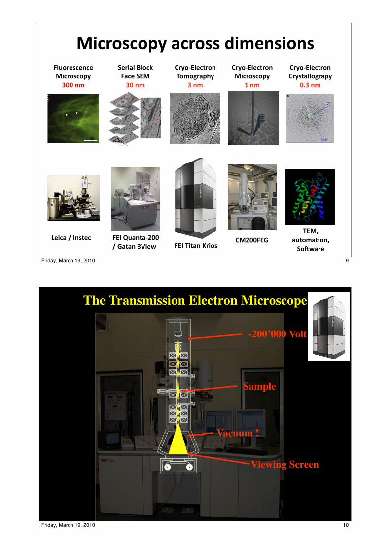
The Transmission Electron Microscope
-200’000 Volt !
Sample
Viewing Screen
Vacuum !
10Friday, March 19, 2010
Transmission Electron Microscope
11Friday, March 19, 2010
Scanning Transmission Electron Microscope
Dark Field DetectorBright Field Detector
12Friday, March 19, 2010
STEM: VG HB-5 (Bioz U-160)
13Friday, March 19, 2010
O-$&"."*P):D-)
*C-.:)%N)'0*C1-
With Guy Cornelis, Biozentrum
Anti LCRV
STEM:
Mueller CA, Broz P, Müller SA, Ringler P, Erne-Brand F, Sorg I, Kuhn M, Engel A, Cornelis GR, Science. 2005 Oct 28;310(5748):674-6
14Friday, March 19, 2010
4B7!P)N$%,)!*&&):%)4D*'-
Mueller et al, J Mol Biol 99
15Friday, March 19, 2010
Z-contrast Image
Spectrometer
Annular Detector
Incident Probe
CCD-EELS Detector
Scanning Transmission Electron Microscopy
Z-Contrast Image – electrons scattered to high angles
Electron Energy Loss Spectrum – inelasticallyscattered electrons
A small probe is scanned
16Friday, March 19, 2010
viewing screen or CCD camera
specimen
electron source
probe!forming lens
defocus
Cowley, J. Elec Microsc Tech 3, 25 (1986)
u
v
Electron Ronchigram
17Friday, March 19, 2010
Disk of Least Confusion
Effect of Spherical Aberrations on the Ronchigram
18Friday, March 19, 2010
James and Browning, Ultramicroscopy 78, 125 (1999)
Effect of Spherical Aberrations on the Ronchigram
Disk of Least Confusion
19Friday, March 19, 2010
overfocused
underfocused
!f=0 nm Scherzer focus !f=-100 nm !f=-150 nm
!f=-200 nm !f=-300 nm !f=-350 nm
!f=100 nm !f=50 nm!f=150 nm
Ronchigrams from Si <110>
20Friday, March 19, 2010
Incident Probe
High-angle annular dark field (HAADF, 20...150 mrad), annular dark field (ADF, 10...20 mrad),
and bright field (BF, 0...10 mrad) detectors
STEM Imaging without an aberration corrector
21Friday, March 19, 2010
Electron Energy Loss Spectroscopy
Complements the Z-contrastImage
-Gives bonding and chemical Information
-The probe can be stopped anywhere in the image anda spectrum can be acquired
22Friday, March 19, 2010
EF
Evac
K
L
Sec
ondar
y E
lect
ron
AugerLight
X-Ray
INNER SHELL OUTER SHELL DE-EXCITATION
R. F. Egerton, EELS in the Electron Microscope, Plenum 1996
Electronic Excitations in the Microscope
23Friday, March 19, 2010
Main Regions of the EEL Spectrum
Direct Beam and LowLoss give thickness information
Core Losses give chemical and bonding information
24Friday, March 19, 2010
Applications
25Friday, March 19, 2010
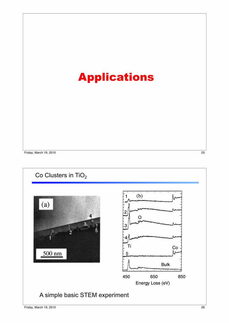
Co Clusters in TiO2
A simple basic STEM experiment
26Friday, March 19, 2010
20 nm 5 nm
Regular Faceted Structure to the Dots Observed Outside the Layers
Y. Lei et al, Applied Physics Letters 82, 4262-4264 (2003)
Tin Quantum Dots in Si
27Friday, March 19, 2010
Direct Observation of Atomic Scale Defects
Twist Boundary in BSCCO Dislocation in YBCO
Grain Boundary In STO
28Friday, March 19, 2010
[0001] 2 nm0 1 2 3 4 5
Energy (keV)In
tensi
ty
Y/Al= !1.3 at%
Grain boundaryO Al
Y
O Al Grain interior
TEM/EDS Observation
HRTEM Image of the Y-doped GB Energy Dispersive Spectroscopy
- EDS reveals that Y is high confined to the GB plane
- However, the location of along the GB plane can not be determined
29Friday, March 19, 2010
STEM Image - Y-doped Boundary
-The basic grain boundary structure is relatively unaltered in comparison to the undoped case.
-The location of the Y ions are revealed by the STEM image


![Ultrafast transmission electron microscopy using a laser ...transmission electron microscopy [4], scanning electron microscopy [5], x-ray diffraction [6], scanning tunneling and atomic](https://static.documents.pub/doc/80x56/607eb1335ce8082131294459/ultrafast-transmission-electron-microscopy-using-a-laser-transmission-electron.jpg)


